WO2014106929A1 - 表示装置、駆動装置、駆動方法、および電子機器 - Google Patents
表示装置、駆動装置、駆動方法、および電子機器 Download PDFInfo
- Publication number
- WO2014106929A1 WO2014106929A1 PCT/JP2013/083962 JP2013083962W WO2014106929A1 WO 2014106929 A1 WO2014106929 A1 WO 2014106929A1 JP 2013083962 W JP2013083962 W JP 2013083962W WO 2014106929 A1 WO2014106929 A1 WO 2014106929A1
- Authority
- WO
- WIPO (PCT)
- Prior art keywords
- voltage
- terminal
- transistor
- period
- display device
- Prior art date
- Legal status (The legal status is an assumption and is not a legal conclusion. Google has not performed a legal analysis and makes no representation as to the accuracy of the status listed.)
- Ceased
Links
Images








Classifications
-
- G—PHYSICS
- G09—EDUCATION; CRYPTOGRAPHY; DISPLAY; ADVERTISING; SEALS
- G09G—ARRANGEMENTS OR CIRCUITS FOR CONTROL OF INDICATING DEVICES USING STATIC MEANS TO PRESENT VARIABLE INFORMATION
- G09G3/00—Control arrangements or circuits, of interest only in connection with visual indicators other than cathode-ray tubes
- G09G3/20—Control arrangements or circuits, of interest only in connection with visual indicators other than cathode-ray tubes for presentation of an assembly of a number of characters, e.g. a page, by composing the assembly by combination of individual elements arranged in a matrix no fixed position being assigned to or needed to be assigned to the individual characters or partial characters
- G09G3/22—Control arrangements or circuits, of interest only in connection with visual indicators other than cathode-ray tubes for presentation of an assembly of a number of characters, e.g. a page, by composing the assembly by combination of individual elements arranged in a matrix no fixed position being assigned to or needed to be assigned to the individual characters or partial characters using controlled light sources
- G09G3/30—Control arrangements or circuits, of interest only in connection with visual indicators other than cathode-ray tubes for presentation of an assembly of a number of characters, e.g. a page, by composing the assembly by combination of individual elements arranged in a matrix no fixed position being assigned to or needed to be assigned to the individual characters or partial characters using controlled light sources using electroluminescent panels
- G09G3/32—Control arrangements or circuits, of interest only in connection with visual indicators other than cathode-ray tubes for presentation of an assembly of a number of characters, e.g. a page, by composing the assembly by combination of individual elements arranged in a matrix no fixed position being assigned to or needed to be assigned to the individual characters or partial characters using controlled light sources using electroluminescent panels semiconductive, e.g. using light-emitting diodes [LED]
- G09G3/3208—Control arrangements or circuits, of interest only in connection with visual indicators other than cathode-ray tubes for presentation of an assembly of a number of characters, e.g. a page, by composing the assembly by combination of individual elements arranged in a matrix no fixed position being assigned to or needed to be assigned to the individual characters or partial characters using controlled light sources using electroluminescent panels semiconductive, e.g. using light-emitting diodes [LED] organic, e.g. using organic light-emitting diodes [OLED]
- G09G3/3225—Control arrangements or circuits, of interest only in connection with visual indicators other than cathode-ray tubes for presentation of an assembly of a number of characters, e.g. a page, by composing the assembly by combination of individual elements arranged in a matrix no fixed position being assigned to or needed to be assigned to the individual characters or partial characters using controlled light sources using electroluminescent panels semiconductive, e.g. using light-emitting diodes [LED] organic, e.g. using organic light-emitting diodes [OLED] using an active matrix
- G09G3/3258—Control arrangements or circuits, of interest only in connection with visual indicators other than cathode-ray tubes for presentation of an assembly of a number of characters, e.g. a page, by composing the assembly by combination of individual elements arranged in a matrix no fixed position being assigned to or needed to be assigned to the individual characters or partial characters using controlled light sources using electroluminescent panels semiconductive, e.g. using light-emitting diodes [LED] organic, e.g. using organic light-emitting diodes [OLED] using an active matrix with pixel circuitry controlling the voltage across the light-emitting element
-
- G—PHYSICS
- G09—EDUCATION; CRYPTOGRAPHY; DISPLAY; ADVERTISING; SEALS
- G09G—ARRANGEMENTS OR CIRCUITS FOR CONTROL OF INDICATING DEVICES USING STATIC MEANS TO PRESENT VARIABLE INFORMATION
- G09G3/00—Control arrangements or circuits, of interest only in connection with visual indicators other than cathode-ray tubes
- G09G3/007—Use of pixel shift techniques, e.g. by mechanical shift of the physical pixels or by optical shift of the perceived pixels
-
- G—PHYSICS
- G09—EDUCATION; CRYPTOGRAPHY; DISPLAY; ADVERTISING; SEALS
- G09G—ARRANGEMENTS OR CIRCUITS FOR CONTROL OF INDICATING DEVICES USING STATIC MEANS TO PRESENT VARIABLE INFORMATION
- G09G3/00—Control arrangements or circuits, of interest only in connection with visual indicators other than cathode-ray tubes
- G09G3/20—Control arrangements or circuits, of interest only in connection with visual indicators other than cathode-ray tubes for presentation of an assembly of a number of characters, e.g. a page, by composing the assembly by combination of individual elements arranged in a matrix no fixed position being assigned to or needed to be assigned to the individual characters or partial characters
- G09G3/22—Control arrangements or circuits, of interest only in connection with visual indicators other than cathode-ray tubes for presentation of an assembly of a number of characters, e.g. a page, by composing the assembly by combination of individual elements arranged in a matrix no fixed position being assigned to or needed to be assigned to the individual characters or partial characters using controlled light sources
- G09G3/30—Control arrangements or circuits, of interest only in connection with visual indicators other than cathode-ray tubes for presentation of an assembly of a number of characters, e.g. a page, by composing the assembly by combination of individual elements arranged in a matrix no fixed position being assigned to or needed to be assigned to the individual characters or partial characters using controlled light sources using electroluminescent panels
- G09G3/32—Control arrangements or circuits, of interest only in connection with visual indicators other than cathode-ray tubes for presentation of an assembly of a number of characters, e.g. a page, by composing the assembly by combination of individual elements arranged in a matrix no fixed position being assigned to or needed to be assigned to the individual characters or partial characters using controlled light sources using electroluminescent panels semiconductive, e.g. using light-emitting diodes [LED]
- G09G3/3208—Control arrangements or circuits, of interest only in connection with visual indicators other than cathode-ray tubes for presentation of an assembly of a number of characters, e.g. a page, by composing the assembly by combination of individual elements arranged in a matrix no fixed position being assigned to or needed to be assigned to the individual characters or partial characters using controlled light sources using electroluminescent panels semiconductive, e.g. using light-emitting diodes [LED] organic, e.g. using organic light-emitting diodes [OLED]
- G09G3/3225—Control arrangements or circuits, of interest only in connection with visual indicators other than cathode-ray tubes for presentation of an assembly of a number of characters, e.g. a page, by composing the assembly by combination of individual elements arranged in a matrix no fixed position being assigned to or needed to be assigned to the individual characters or partial characters using controlled light sources using electroluminescent panels semiconductive, e.g. using light-emitting diodes [LED] organic, e.g. using organic light-emitting diodes [OLED] using an active matrix
- G09G3/3233—Control arrangements or circuits, of interest only in connection with visual indicators other than cathode-ray tubes for presentation of an assembly of a number of characters, e.g. a page, by composing the assembly by combination of individual elements arranged in a matrix no fixed position being assigned to or needed to be assigned to the individual characters or partial characters using controlled light sources using electroluminescent panels semiconductive, e.g. using light-emitting diodes [LED] organic, e.g. using organic light-emitting diodes [OLED] using an active matrix with pixel circuitry controlling the current through the light-emitting element
-
- G—PHYSICS
- G09—EDUCATION; CRYPTOGRAPHY; DISPLAY; ADVERTISING; SEALS
- G09G—ARRANGEMENTS OR CIRCUITS FOR CONTROL OF INDICATING DEVICES USING STATIC MEANS TO PRESENT VARIABLE INFORMATION
- G09G3/00—Control arrangements or circuits, of interest only in connection with visual indicators other than cathode-ray tubes
- G09G3/20—Control arrangements or circuits, of interest only in connection with visual indicators other than cathode-ray tubes for presentation of an assembly of a number of characters, e.g. a page, by composing the assembly by combination of individual elements arranged in a matrix no fixed position being assigned to or needed to be assigned to the individual characters or partial characters
- G09G3/22—Control arrangements or circuits, of interest only in connection with visual indicators other than cathode-ray tubes for presentation of an assembly of a number of characters, e.g. a page, by composing the assembly by combination of individual elements arranged in a matrix no fixed position being assigned to or needed to be assigned to the individual characters or partial characters using controlled light sources
- G09G3/30—Control arrangements or circuits, of interest only in connection with visual indicators other than cathode-ray tubes for presentation of an assembly of a number of characters, e.g. a page, by composing the assembly by combination of individual elements arranged in a matrix no fixed position being assigned to or needed to be assigned to the individual characters or partial characters using controlled light sources using electroluminescent panels
- G09G3/32—Control arrangements or circuits, of interest only in connection with visual indicators other than cathode-ray tubes for presentation of an assembly of a number of characters, e.g. a page, by composing the assembly by combination of individual elements arranged in a matrix no fixed position being assigned to or needed to be assigned to the individual characters or partial characters using controlled light sources using electroluminescent panels semiconductive, e.g. using light-emitting diodes [LED]
- G09G3/3208—Control arrangements or circuits, of interest only in connection with visual indicators other than cathode-ray tubes for presentation of an assembly of a number of characters, e.g. a page, by composing the assembly by combination of individual elements arranged in a matrix no fixed position being assigned to or needed to be assigned to the individual characters or partial characters using controlled light sources using electroluminescent panels semiconductive, e.g. using light-emitting diodes [LED] organic, e.g. using organic light-emitting diodes [OLED]
- G09G3/3266—Details of drivers for scan electrodes
-
- G—PHYSICS
- G09—EDUCATION; CRYPTOGRAPHY; DISPLAY; ADVERTISING; SEALS
- G09G—ARRANGEMENTS OR CIRCUITS FOR CONTROL OF INDICATING DEVICES USING STATIC MEANS TO PRESENT VARIABLE INFORMATION
- G09G2230/00—Details of flat display driving waveforms
-
- G—PHYSICS
- G09—EDUCATION; CRYPTOGRAPHY; DISPLAY; ADVERTISING; SEALS
- G09G—ARRANGEMENTS OR CIRCUITS FOR CONTROL OF INDICATING DEVICES USING STATIC MEANS TO PRESENT VARIABLE INFORMATION
- G09G2300/00—Aspects of the constitution of display devices
- G09G2300/04—Structural and physical details of display devices
- G09G2300/0404—Matrix technologies
- G09G2300/0408—Integration of the drivers onto the display substrate
-
- G—PHYSICS
- G09—EDUCATION; CRYPTOGRAPHY; DISPLAY; ADVERTISING; SEALS
- G09G—ARRANGEMENTS OR CIRCUITS FOR CONTROL OF INDICATING DEVICES USING STATIC MEANS TO PRESENT VARIABLE INFORMATION
- G09G2300/00—Aspects of the constitution of display devices
- G09G2300/08—Active matrix structure, i.e. with use of active elements, inclusive of non-linear two terminal elements, in the pixels together with light emitting or modulating elements
- G09G2300/0809—Several active elements per pixel in active matrix panels
- G09G2300/0819—Several active elements per pixel in active matrix panels used for counteracting undesired variations, e.g. feedback or autozeroing
-
- G—PHYSICS
- G09—EDUCATION; CRYPTOGRAPHY; DISPLAY; ADVERTISING; SEALS
- G09G—ARRANGEMENTS OR CIRCUITS FOR CONTROL OF INDICATING DEVICES USING STATIC MEANS TO PRESENT VARIABLE INFORMATION
- G09G2300/00—Aspects of the constitution of display devices
- G09G2300/08—Active matrix structure, i.e. with use of active elements, inclusive of non-linear two terminal elements, in the pixels together with light emitting or modulating elements
- G09G2300/0809—Several active elements per pixel in active matrix panels
- G09G2300/0842—Several active elements per pixel in active matrix panels forming a memory circuit, e.g. a dynamic memory with one capacitor
-
- G—PHYSICS
- G09—EDUCATION; CRYPTOGRAPHY; DISPLAY; ADVERTISING; SEALS
- G09G—ARRANGEMENTS OR CIRCUITS FOR CONTROL OF INDICATING DEVICES USING STATIC MEANS TO PRESENT VARIABLE INFORMATION
- G09G2310/00—Command of the display device
- G09G2310/02—Addressing, scanning or driving the display screen or processing steps related thereto
- G09G2310/0264—Details of driving circuits
- G09G2310/0272—Details of drivers for data electrodes, the drivers communicating data to the pixels by means of a current
-
- G—PHYSICS
- G09—EDUCATION; CRYPTOGRAPHY; DISPLAY; ADVERTISING; SEALS
- G09G—ARRANGEMENTS OR CIRCUITS FOR CONTROL OF INDICATING DEVICES USING STATIC MEANS TO PRESENT VARIABLE INFORMATION
- G09G2310/00—Command of the display device
- G09G2310/02—Addressing, scanning or driving the display screen or processing steps related thereto
- G09G2310/0264—Details of driving circuits
- G09G2310/0291—Details of output amplifiers or buffers arranged for use in a driving circuit
-
- G—PHYSICS
- G09—EDUCATION; CRYPTOGRAPHY; DISPLAY; ADVERTISING; SEALS
- G09G—ARRANGEMENTS OR CIRCUITS FOR CONTROL OF INDICATING DEVICES USING STATIC MEANS TO PRESENT VARIABLE INFORMATION
- G09G2330/00—Aspects of power supply; Aspects of display protection and defect management
- G09G2330/02—Details of power systems and of start or stop of display operation
- G09G2330/021—Power management, e.g. power saving
-
- G—PHYSICS
- G09—EDUCATION; CRYPTOGRAPHY; DISPLAY; ADVERTISING; SEALS
- G09G—ARRANGEMENTS OR CIRCUITS FOR CONTROL OF INDICATING DEVICES USING STATIC MEANS TO PRESENT VARIABLE INFORMATION
- G09G3/00—Control arrangements or circuits, of interest only in connection with visual indicators other than cathode-ray tubes
- G09G3/20—Control arrangements or circuits, of interest only in connection with visual indicators other than cathode-ray tubes for presentation of an assembly of a number of characters, e.g. a page, by composing the assembly by combination of individual elements arranged in a matrix no fixed position being assigned to or needed to be assigned to the individual characters or partial characters
- G09G3/22—Control arrangements or circuits, of interest only in connection with visual indicators other than cathode-ray tubes for presentation of an assembly of a number of characters, e.g. a page, by composing the assembly by combination of individual elements arranged in a matrix no fixed position being assigned to or needed to be assigned to the individual characters or partial characters using controlled light sources
- G09G3/30—Control arrangements or circuits, of interest only in connection with visual indicators other than cathode-ray tubes for presentation of an assembly of a number of characters, e.g. a page, by composing the assembly by combination of individual elements arranged in a matrix no fixed position being assigned to or needed to be assigned to the individual characters or partial characters using controlled light sources using electroluminescent panels
- G09G3/32—Control arrangements or circuits, of interest only in connection with visual indicators other than cathode-ray tubes for presentation of an assembly of a number of characters, e.g. a page, by composing the assembly by combination of individual elements arranged in a matrix no fixed position being assigned to or needed to be assigned to the individual characters or partial characters using controlled light sources using electroluminescent panels semiconductive, e.g. using light-emitting diodes [LED]
- G09G3/3208—Control arrangements or circuits, of interest only in connection with visual indicators other than cathode-ray tubes for presentation of an assembly of a number of characters, e.g. a page, by composing the assembly by combination of individual elements arranged in a matrix no fixed position being assigned to or needed to be assigned to the individual characters or partial characters using controlled light sources using electroluminescent panels semiconductive, e.g. using light-emitting diodes [LED] organic, e.g. using organic light-emitting diodes [OLED]
- G09G3/3275—Details of drivers for data electrodes
- G09G3/3291—Details of drivers for data electrodes in which the data driver supplies a variable data voltage for setting the current through, or the voltage across, the light-emitting elements
Definitions
- the present disclosure relates to a display device having a current-driven display element, a driving device and a driving method used in such a display device, and an electronic apparatus including such a display device.
- a display device that uses a current-driven optical element whose emission luminance changes according to a flowing current value, for example, an organic EL (Electro-Luminescence) element, as a light emitting element.
- Display devices have been developed and commercialized. Unlike a liquid crystal element or the like, a light emitting element is a self light emitting element and does not require a light source (backlight). Therefore, the organic EL display device has features such as higher image visibility, lower power consumption, and faster element response speed than a liquid crystal display device that requires a light source.
- Patent Document 1 discloses a display panel including a pixel array unit and a control line driving unit including a shift register and a plurality of buffer circuits.
- the control driving unit supplies a control signal to the pixels via the control line.
- the buffer circuit is supplied with at least two voltages (VDD / VSS), and selects and outputs one of these voltages based on a set signal and a reset signal supplied from the outside. It has become.
- electronic circuits are desired to have a simple configuration from the viewpoint of cost, circuit layout area, degree of freedom of circuit layout, and the like, and a simple configuration is also expected for a driver circuit in a display device.
- the display device includes a unit pixel, a switch, and a nonlinear element.
- the switch performs on / off control between the second terminal to which the DC signal is applied and the third terminal connected to the unit pixel, based on the pulse signal applied to the first terminal.
- the non-linear element is inserted between the first terminal and the third terminal.
- the drive device includes a switch and a nonlinear element.
- the switch performs on / off control between the second terminal to which the DC signal is applied and the third terminal connected to the unit pixel, based on the pulse signal applied to the first terminal.
- the non-linear element is inserted between the first terminal and the third terminal.
- a driving method is based on the pulse signal applied to the first terminal, between the second terminal to which the DC signal is applied and the third terminal connected to the unit pixel. On-off control is performed, and nonlinear operation is performed between the first terminal and the third terminal.
- An electronic apparatus includes the display device, and includes, for example, a mobile terminal device such as a television device, a digital camera, a personal computer, a video camera, or a mobile phone.
- a mobile terminal device such as a television device, a digital camera, a personal computer, a video camera, or a mobile phone.
- a signal is applied to the unit pixel based on the pulse signal.
- the switch is on / off controlled between the second terminal to which the DC signal is applied and the third terminal to which the unit pixel is connected, A non-linear operation is performed by a non-linear element between the first terminal and the third terminal.
- the second terminal and the unit pixel to which the DC signal is applied based on the pulse signal applied to the first terminal A simple circuit is realized by providing a switch for on / off control between the third terminal connected to the terminal and a non-linear element inserted between the first terminal and the third terminal. it can.
- FIG. 11 is a block diagram illustrating a configuration example of a display device according to an embodiment of the present disclosure.
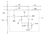
- FIG. 2 is a circuit diagram illustrating a configuration example of a subpixel illustrated in FIG. 1.
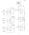
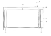
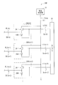
- FIG. 2 is a circuit diagram illustrating a configuration example of a power supply line driving unit illustrated in FIG. 1. It is explanatory drawing showing arrangement
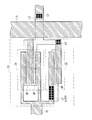
- FIG. 4 is a layout diagram illustrating a layout configuration example of a drive circuit and its peripheral portion illustrated in FIG. 3.
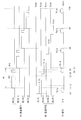
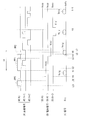
- FIG. 6 is a timing waveform diagram illustrating an operation example of the drive unit according to the first embodiment.
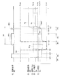
- FIG. 6 is a timing waveform diagram illustrating an operation example of a sub-pixel according to the first embodiment.
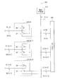
- FIG. 4 is a timing waveform diagram illustrating an operation example of the drive circuit illustrated in FIG. 3. It is a circuit diagram showing the example of 1 structure of the power supply line drive part which concerns on a comparative example.
- FIG. 10 is a timing waveform diagram illustrating an operation example of the drive circuit illustrated in FIG. 9.
- FIG. 6 is a circuit diagram illustrating a configuration example of a power supply line driving unit according to a modification of the first embodiment. It is a circuit diagram showing the example of 1 structure of the power supply line drive part which concerns on the other modification of 1st Embodiment.
- FIG. 10 is a timing waveform diagram illustrating an operation example of a drive unit according to the second embodiment.
- FIG. 10 is a timing waveform diagram illustrating an operation example of a sub-pixel according to the second embodiment.
- FIG. 9 is a timing waveform diagram illustrating an operation example of a drive circuit according to a second embodiment. It is explanatory drawing showing the operation example of the drive circuit which concerns on 2nd Embodiment, and a sub pixel. It is a circuit diagram showing the example of 1 composition of the sub pixel concerning the modification of a 2nd embodiment. It is explanatory drawing showing the example of 1 structure of the module which mounted the display apparatus which concerns on embodiment. It is a perspective view showing the external appearance structure of the application example 1 of the display apparatus which concerns on embodiment. It is a perspective view showing the external appearance structure of the application example 2 of the display apparatus which concerns on embodiment.
- FIG. 1 illustrates a configuration example of a display device according to the first embodiment.
- the display device 1 is an active matrix display device using organic EL elements.
- the drive device and the drive method according to the embodiment of the present disclosure are embodied by the present embodiment, they will be described together.
- the display device 1 includes a display unit 10 and a drive unit 20.
- the display unit 10 has a plurality of pixels Pix arranged in a matrix. Each pixel Pix has red, green, and blue sub-pixels 11.
- the display unit 10 includes a plurality of scanning lines WSL and a plurality of power supply lines PL extending in the row direction, and a plurality of data lines DTL extending in the column direction. One ends of these scanning lines WSL, power supply lines PL, and data lines DTL are connected to the drive unit 20.
- Each of the sub-pixels 11 described above is disposed at the intersection of the scanning line WSL and the data line DTL.
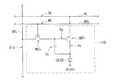
- FIG. 2 shows an example of the circuit configuration of the sub-pixel 11.
- the subpixel 11 includes a write transistor WSTr, a drive transistor DRTr, an organic EL element OLED, and capacitive elements Cs and Csub. That is, in this example, the sub-pixel 11 has a so-called “2Tr2C” configuration including two transistors (the write transistor WSTr and the drive transistor DRTr) and the two capacitance elements Cs and Csub. .
- the write transistor WSTr and the drive transistor DRTr are composed of, for example, an N-channel MOS (Metal Oxide Semiconductor) type TFT (Thin Film Transistor).
- the write transistor WSTr has a gate connected to the scanning line WSL, a source connected to the data line DTL, and a drain connected to the gate of the drive transistor DRTr and one end of the capacitive element Cs.
- the drive transistor DRTr has a gate connected to the drain of the write transistor WSTr and one end of the capacitive element Cs, a drain connected to the power supply line PL, and a source connected to the other end of the capacitive element Cs and the anode of the organic EL element OLED. Has been.
- the capacitor element Cs has one end connected to the gate or the like of the drive transistor DRTr and the other end connected to the source or the like of the drive transistor DRTr.
- the capacitive element Csub has one end connected to the anode of the organic EL element OLED and the other end connected to the cathode of the organic EL element OLED. That is, in this example, the capacitive element Csub is connected in parallel with the organic EL element OLED.
- the organic EL element OLED is a light emitting element that emits light of a color (red, green, blue) corresponding to each sub-pixel 11, an anode is connected to a source of the driving transistor DRTr and the like, and a driving unit 20 is connected to the cathode.
- the cathode voltage Vcath is supplied.
- the drive unit 20 drives the display unit 10 based on the video signal Sdisp and the synchronization signal Ssync supplied from the outside.
- the driving unit 20 includes a video signal processing unit 21, a timing generation unit 22, a scanning line driving unit 23, a power line driving unit 26, and a data line driving unit 27. Yes.
- the video signal processing unit 21 performs predetermined signal processing on the video signal Sdisp supplied from the outside to generate a video signal Sdisp2.
- Examples of the predetermined signal processing include gamma correction and overdrive correction.
- the timing generation unit 22 supplies control signals to the scanning line driving unit 23, the power supply line driving unit 26, and the data line driving unit 27 based on the synchronization signal Ssync supplied from the outside, and these are mutually connected. It is a circuit that controls to operate in synchronization.
- the scanning line driving unit 23 sequentially selects the sub-pixels 11 for each row by sequentially applying the scanning signal WS to the plurality of scanning lines WSL in accordance with the control signal supplied from the timing generation unit 22. .
- the power supply line driving unit 26 sequentially applies the power supply signal DS to the plurality of power supply lines PL in accordance with the control signal supplied from the timing generation unit 22, thereby performing the light emission operation and the extinction operation of the subpixels 11 for each row. Control is performed.
- the power signal DS transitions between the voltage Vccp and the voltage Vini.
- the voltage Vini is a voltage for initializing the sub-pixel 11
- the voltage Vccp is a voltage for causing the organic EL element OLED to emit light by flowing a current Ids through the driving transistor DRTr.
- FIG. 3 shows a configuration example of the power supply line driving unit 26.
- the power supply line drive unit 26 includes a voltage generation unit 31, a shift register 32, and a plurality of drive circuits 33.
- the voltage generator 31 generates a voltage Vccp.
- the voltage generator 31 supplies the voltage Vccp to each drive circuit 33 via the wiring L1.
- the shift register 32 generates a plurality of scanning signals Ss for selecting a pixel line to be driven based on a control signal (not shown) supplied from the timing generator 22.
- Each scanning signal Ss corresponds to each pixel line in the display unit 10.
- the kth scanning signal Ss (k) corresponds to the kth pixel line.
- Each scanning signal Ss is a signal that transitions between a high level voltage VH and a low level voltage VL.
- the low level voltage VL is lower than the voltage Vini by a threshold voltage Vth of a transistor 35 (described later) of the drive circuit 33 (Vini ⁇ Vth).
- the shift register 32 supplies the scanning signal Ss (k) to the kth drive circuit 33 (k) via the kth wiring L2 (k).
- Each drive circuit 33 generates a power supply signal DS based on the voltage Vccp supplied from the voltage generator 31 and the scanning signal Ss supplied from the shift register 32. Each drive circuit 33 is provided corresponding to each pixel line in the display unit 10. Specifically, for example, the kth drive circuit 33 (k) generates the kth power supply signal DS (k) based on the voltage Vccp and the kth scan signal Ss (k). The drive circuit 33 (k) applies the power signal DS (k) to the power line PL (k) related to the kth pixel line.
- Each drive circuit 33 has transistors 34 and 35.
- the transistors 34 and 35 are composed of, for example, N-channel MOS type TFTs, similarly to the write transistor WSTr and the drive transistor DRTr.
- the gate of the transistor 34 is connected to the source of the transistor 35 and the wiring L2 (k)
- the drain is connected to the wiring L1
- the source is connected to the drain and gate of the transistor 35.
- the power supply line PL (k) In addition to being connected, it is connected to the power supply line PL (k).
- the drain of the transistor 35 is connected to the gate of the transistor 35 and the source of the transistor 34 and to the power supply line PL (k), and the source is connected to the gate of the transistor 34. It is connected to the wiring L2 (k). That is, the transistor 35 is so-called diode-connected.
- the transistor 34 is formed with a channel width W wider than the channel width W of the transistor 35.
- FIG. 4 shows the arrangement of the power line drive unit 26 in the display device 1.
- the scanning line drive unit 23 is arranged in the left frame region of the substrate 30 where the display unit 10 is formed, and the power line drive unit 26 is arranged in the right frame region.
- the wiring L1 is provided so as to extend in the vertical direction.
- a shift register 32 is arranged on the right side of the wiring L1, and a plurality of drive circuits 33 are arranged in a region 39 on the left side of the wiring L1.
- FIG. 5 shows a layout configuration example of the drive circuit 33 and its peripheral portion.
- the display device 1 is manufactured using a manufacturing process capable of forming two metal layers, a lower layer metal M1 and an upper layer metal M2.
- the lower layer metal M1 is made of, for example, molybdenum Mo
- the upper layer metal M2 is made of, for example, aluminum Al.
- the sheet resistance of the upper metal M2 is lower than that of the lower metal M1.
- the gates (gate portions GP) of the transistors 34 and 35 are composed of the lower layer metal M1, and the drains and sources of the transistors 34 and 35 are connected to the upper layer metal M2.
- the wiring L1 is formed of an upper layer metal M2, and is connected to the drain of the transistor 34.
- the wiring L2 is formed of the upper layer metal M2 at a portion other than the portion intersecting with the wiring L1, and is formed of the lower layer metal M1 at a portion intersecting with the wiring L1.
- the wiring L2 is connected to the gate (gate portion GP) of the transistor 34 and to the upper metal M2 connected to the source of the transistor 35 via a contact CT.
- the power supply line PL is formed of the upper layer metal M2, is connected to the source of the transistor 34 and the drain of the transistor 35, and is connected to the gate of the transistor 35 through the contact CT.
- the data line driving unit 27 includes a pixel voltage Vsig that indicates the emission luminance of each sub-pixel 11 according to the video signal Sdisp2 supplied from the video signal processing unit 21 and the control signal supplied from the timing generation unit 22.
- a signal Sig including a voltage Vofs for performing Vth correction described later is generated and applied to each data line DTL.
- the drive unit 20 performs correction (Vth correction) on the sub-pixel 11 to suppress the influence of the element variation of the drive transistor DRTr on the image quality. Thereafter, the pixel voltage Vsig is written to the sub-pixel 11 and ⁇ (mobility) correction different from the above-described Vth correction is performed. After that, the organic EL element OLED of the sub-pixel 11 emits light with a luminance corresponding to the written pixel voltage Vsig.
- the sub-pixel 11 corresponds to a specific example of “unit pixel” in the present disclosure.
- the capacitive element Cs corresponds to a specific example of “first capacitive element” in the present disclosure.
- the capacitive element Csub corresponds to a specific example of “second capacitive element” in the present disclosure.
- the organic EL element OLED corresponds to a specific example of “display element” in the present disclosure.
- the transistor 34 corresponds to a specific example of “switch” in the present disclosure.
- the transistor 35 corresponds to a specific example of “nonlinear element” in the present disclosure.
- the scanning signal Ss corresponds to a specific example of “pulse signal” in the present disclosure.
- the wiring L2 corresponds to a specific example of “first wiring” in the present disclosure
- the wiring L1 corresponds to a specific example of “second wiring” in the present disclosure
- the high level voltage VH corresponds to a specific example of “first voltage” in the present disclosure
- the low level voltage VL corresponds to a specific example of “second voltage” in the present disclosure
- the voltage Vini corresponds to a specific example of “third voltage” in the present disclosure
- the voltage Vccp corresponds to a specific example of “fourth voltage” in the present disclosure
- the voltage Vofs corresponds to a specific example of “reset voltage” in the present disclosure.
- the video signal processing unit 21 performs predetermined signal processing on the video signal Sdisp supplied from the outside to generate a video signal Sdisp2.
- the timing generation unit 22 supplies control signals to the scanning line driving unit 23, the power supply line driving unit 26, and the data line driving unit 27 based on the synchronization signal Ssync supplied from the outside, and these are synchronized with each other. And control to work.
- the scanning line driving unit 23 sequentially selects the sub-pixels 11 for each row by sequentially applying the scanning signal WS to the plurality of scanning lines WSL in accordance with the control signal supplied from the timing generation unit 22.
- the power supply line driving unit 26 sequentially applies the power supply signal DS to the plurality of power supply lines PL in accordance with the control signal supplied from the timing generation unit 22, thereby performing the light emission operation and the extinction operation of the subpixels 11 for each row. Take control.
- the data line driving unit 27 performs pixel voltage Vsig and Vth correction for instructing the light emission luminance of each sub-pixel 11 in accordance with the video signal Sdisp2 supplied from the video signal processing unit 21 and the control signal supplied from the timing generation unit 22.
- a signal Sig including a voltage Vofs for performing is generated and applied to each data line DTL.
- the display unit 10 performs display based on the scanning signal WS, the power supply signal DS, and the signal Sig supplied from the driving unit 20.
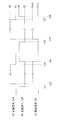
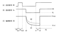
- FIG. 6A and 6B are timing charts of the operation of the drive unit 20.
- FIG. 6A shows the waveform of the scanning signal WS
- FIG. 6B shows the waveform of the power supply signal DS
- FIG. 6C shows the waveform of the signal Sig. Indicates.
- a scanning signal WS (k) is a scanning signal WS for driving the sub-pixel 11 in the k-th line
- the scanning signals WS (k + 1), WS (k + 2), WS (K + 3) are scanning signals WS for driving the sub-pixels 11 of the (k + 1) th line, the (k + 2) th line, and the (k + 3) th line, respectively.
- the scanning line driving unit 23 of the driving unit 20 sequentially applies a scanning signal WS having two pulses PP1 and PP2 to the scanning line WSL (FIG. 6A). At that time, the scanning line driving unit 23 applies two pulses PP1 and PP2 to one scanning line WSL in one horizontal period (1H).
- the power supply line driving unit 26 becomes the voltage Vini only for a predetermined period (for example, a period from timing t0 to t2) including the start timing (for example, timing t1) of the pulse PP1 with respect to the power supply line PL, and becomes the voltage Vccp for the other periods.
- a power supply signal DS is applied (FIG. 6B).
- the data line driving unit 27 applies the pixel voltage Vsig to the data line DTL during a predetermined period including the pulse PP2 (for example, the period from timing t4 to t7), and applies the voltage Vofs during other periods (FIG. 6 ( C)).
- the drive unit 20 drives the k-th sub-pixel 11 in one horizontal period (for example, timings t1 to t7), and (k + 1) line in the next horizontal period (for example, timings t7 to t8).
- the sub-pixel 11 of the eye is driven.
- the driving unit 20 drives all the sub-pixels 11 of the display unit 10 in one frame period.
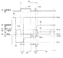
- FIG. 7 shows a timing chart of the operation of the sub-pixel 11 in the period from the timing t0 to t7,
- A shows the waveform of the scanning signal WS
- B shows the waveform of the power supply signal DS
- C shows the waveform of the signal Sig
- D shows the waveform of the gate voltage Vg of the drive transistor DRTr
- E shows the waveform of the source voltage Vs of the drive transistor DRTr.
- 7B to 7E show the waveforms using the same voltage axis.
- the drive unit 20 initializes the sub-pixel 11 within one horizontal period (1H) (initialization period P1), and performs Vth correction for suppressing the influence of the element variation of the drive transistor DRTr on the image quality (Vth In the correction period P2), the pixel voltage Vsig is written to the sub-pixel 11 and ⁇ correction is performed (writing / ⁇ correction period P3). After that, the organic EL element OLED of the sub-pixel 11 emits light with a luminance corresponding to the written pixel voltage Vsig (light emission period P4).
- the initialization period P1 corresponds to a specific example of “first sub period” in the present disclosure
- the Vth correction period P2 corresponds to a specific example of “second sub period” in the present disclosure.
- the power supply line driving unit 26 changes the power supply signal DS from the voltage Vccp to the voltage Vini at the timing t0 prior to the initialization period P1 (FIG. 7B).
- the drive transistor DRTr is turned on, and the source voltage Vs of the drive transistor DRTr is set to the voltage Vini (FIG. 7E).
- the drive unit 20 performs Vth correction during the period from timing t2 to t3 (Vth correction period P2).
- the power supply line drive unit 26 changes the power supply signal DS from the voltage Vini to the voltage Vccp at the timing t2 (FIG. 7B).
- the drive transistor DRTr operates in the saturation region, and a current Ids flows from the drain to the source. With this current Ids, the source voltage Vs rises (FIG. 7E).
- the organic EL element OLED maintains a reverse bias state, and no current flows through the organic EL element OLED.
- the gate-source voltage Vgs decreases, and thus the current Ids decreases.
- the current Ids converges toward “0” (zero).
- the scanning line driving unit 23 changes the voltage of the scanning signal WS from the high level to the low level at timing t3 (FIG. 7A). As a result, the write transistor WSTr is turned off. Then, the data line driving unit 27 sets the signal Sig to the pixel voltage Vsig at timing t4 (FIG. 7C).
- the driving unit 20 writes the pixel voltage Vsig to the sub-pixel 11 and performs ⁇ correction during the period from timing t5 to t6 (writing / ⁇ correction period P3).
- the scanning line driving unit 23 changes the voltage of the scanning signal WS from low level to high level at timing t5 (FIG. 7A). Accordingly, the write transistor WSTr is turned on, and the gate voltage Vg of the drive transistor DRTr rises from the voltage Vofs to the pixel voltage Vsig (FIG. 7D).
- the gate-source voltage Vgs of the drive transistor DRTr becomes larger than the threshold voltage Vth (Vgs> Vth), and the current Ids flows from the drain to the source, so that the source voltage Vs of the drive transistor DRTr rises (FIG. 7 ( E)).
- Vgs> Vth the threshold voltage
- the current Ids flows from the drain to the source, so that the source voltage Vs of the drive transistor DRTr rises
- the influence of element variations of the drive transistor DRTr is suppressed ( ⁇ (mobility) correction)
- the gate-source voltage Vgs of the drive transistor DRTr is set to a voltage Vemi corresponding to the pixel voltage Vsig. Is done.
- the drive unit 20 causes the sub-pixel 11 to emit light in a period after the timing t6 (light emission period P4).
- the scanning line driving unit 23 changes the voltage of the scanning signal WS from a high level to a low level (FIG. 7A).
- the write transistor WSTr is turned off, and the gate of the drive transistor DRTr becomes floating, so that the voltage between the terminals of the capacitive element Cs, that is, the gate-source voltage Vgs of the drive transistor DRTr is maintained thereafter.
- the source voltage Vs of the drive transistor DRTr increases (FIG.
- the gate voltage Vg of the drive transistor DRTr also increases (FIG. 7D).
- the source voltage Vs of the drive transistor DRTr becomes larger than the threshold voltage Vel of the organic EL element OLED and the voltage Vcath (Vel + Vcath) by such bootstrap operation, the voltage between the anode and the cathode of the organic EL element OLED is increased. A current flows and the organic EL element OLED emits light. That is, the source voltage Vs increases according to the element variation of the organic EL element OLED, and the organic EL element OLED emits light.
- the light emission period P4 shifts to the initialization period P1.
- the drive unit 20 is driven to repeat this series of operations.
- the source voltage Vs is increased in accordance with the element variation of the organic EL element OLED in the light emission period P ⁇ b> 4, so that deterioration in image quality due to the element variation of the organic EL element OLED can be suppressed. it can.
- the drive circuit 33 generates a power signal DS based on the voltage Vccp supplied from the voltage generator 31 and the scanning signal Ss supplied from the shift register 32.
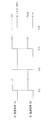
- FIG. 8 shows a timing chart of the operation of the drive circuit 33, (A) shows the waveform of the scanning signal Ss, and (B) shows the waveform of the power supply signal DS.
- the voltage of the scanning signal Ss changes from the low level voltage VL to the high level voltage VH (FIG. 8A).
- the transistor 34 of the drive circuit 33 is turned on, the transistor 35 is turned off, and the voltage Vccp generated by the voltage generator 31 is applied to the power supply line PL via the transistor 34.
- the power supply signal DS changes to the voltage Vccp (FIG. 8B).
- the drive circuit 33 supplies a current to each subpixel 11 connected to the power supply line PL in the Vth correction period P2, the writing / ⁇ correction period P3, and the light emission period P4.
- the drive circuit 33 repeats the above operation. As a result, each subpixel 11 connected to the power supply line PL repeats a series of operations from initialization to light emission.
- the drive circuit 33 is configured using the transistor 34 functioning as a switch and the transistor 35 functioning as a nonlinear element (diode).
- the circuit configuration of the drive unit 26 can be simplified.
- the drive circuit 33 since the channel width W of the transistor 34 is larger than the channel width W of the transistor 35, the sub-pixel 11 can be easily driven and the circuit area of the drive circuit 33 can be reduced. That is, the drive circuit 33 supplies current to the subpixel 11 by turning on the transistor 34 in the Vth correction period P2, the writing / ⁇ correction period P3, and the light emission period P4. In particular, in the light emission period P4, a driving current for supplying light from the organic EL element OLED is supplied. This drive current increases as the light emission luminance of the organic EL element OLED increases. Therefore, it is desirable that the on-resistance of the transistor 34 be sufficiently low, and it is desirable that the channel width W of the transistor 34 be wide.
- the drive circuit 33 applies the voltage Vini to the power supply line PL, and sets the source voltage Vs of the sub-pixel 11 to the voltage Vini.
- the channel width W of the transistor 35 can be reduced.
- the wiring L1 is formed of the upper layer metal M2 having a low sheet resistance, the resistance value of the wiring L1 can be lowered and the subpixel 11 is driven. Can be easier.
- the wiring L1 is disposed between the driving circuit 33 and the shift register 32, so that the sub-pixels 11 can be easily driven. That is, for example, when the wiring L1 is disposed between the display unit 10 and the drive circuit 33, the wiring L1 and the power supply line PL cross each other. That is, in this case, it is necessary to form the wiring L1 or the power supply line PL with the lower layer metal M1 having a high sheet resistance, and a parasitic capacitance is formed at the intersection. As a result, the rise time tr of the power supply signal DS applied to the power supply line PL becomes longer, and for example, it may be difficult to generate a pulse having a short time width.
- the wiring L1 is disposed between the drive circuit 33 and the shift register 32. Therefore, the wiring L1 can be formed of the upper layer metal M2 having a low sheet resistance, and the power signal DS rises. The time tr can be shortened.
- the wiring L1 and the wiring L2 intersect, and the wiring L2 needs to be formed of the lower layer metal M1 having a high sheet resistance at the intersection.
- the wiring L2 is connected to the transistors 33 and 34, and unlike the power supply line PL extending into the display panel 10, since the capacitive load is small, the shift register 32 can relatively easily connect the wiring L2. Can be driven. Therefore, the possibility that the waveform of the power supply signal DS becomes dull can be reduced.
- FIG. 9 shows a configuration example of the power supply line driving unit 26R according to the comparative example.
- the power line driver 26R includes a voltage generator 31R, shift registers 32RA and 32RB, and a plurality of driver circuits 33R.
- the voltage generation unit 31R generates the voltage Vccp, supplies the voltage Vccp to each drive circuit 33R via the wiring L1, generates the voltage Vini, and supplies the voltage Vini to each drive circuit via the wiring L3. 33R is supplied.
- the shift register 32RA generates a plurality of scanning signals SsA for selecting a pixel line to be driven based on a control signal (not shown) supplied from the timing generator 22. For example, the shift register 32RA supplies the scanning signal SsA (k) to the kth driving circuit 33R (k) via the kth wiring L2A (k). Similarly, the shift register 32RB generates a plurality of scanning signals SsB for selecting a pixel line to be driven based on a control signal (not shown) supplied from the timing generation unit 22. For example, the shift register 32RB supplies the scanning signal SsB (k) to the kth drive circuit 33R (k) via the kth wiring L2B (k).
- Each drive circuit 33R generates the power supply signal DS based on the voltages Vccp and Vini supplied from the voltage generation unit 31R, the scanning signal SsA supplied from the shift register 33RA, and the scanning signal SsB supplied from the shift register 33RB. To do.
- Each drive circuit 33R includes a transistor 35R.
- the transistor 35R is configured by, for example, an N-channel MOS type TFT, similarly to the transistor 34 and the like.
- the drain of the transistor 35R is connected to the source of the transistor 34 and to the power supply line PL (k), the gate is connected to the wiring L2B (k), and the source is connected to the wiring L3. Is done.
- FIG. 10 shows a timing chart of the operation of the drive circuit 33R.
- A shows the waveform of the scanning signal SsA
- B shows the waveform of the scanning signal SsB
- C shows the power supply signal DS. Waveform is shown.
- the voltage of the scanning signal SsB changes from the high level voltage VH to the low level voltage VL (FIG. 10B).
- the transistor 35R is turned off, and the application of the voltage Vini to the power supply line PL is stopped.
- the voltage of the scanning signal SsA changes from the low level voltage VL to the high level voltage VH (FIG. 10A).
- the transistor 34 is turned on, the voltage Vccp generated by the voltage generator 31R is applied to the power supply line PL through the transistor 34, and the power supply signal DS changes to the voltage Vccp (FIG. 10C).
- the voltage of the scanning signal SsA changes from the high level voltage VH to the low level voltage VL (FIG. 10A).
- the transistor 34 is turned off, and the application of the voltage Vccp to the power supply line PL is stopped.
- the voltage of the scanning signal SsB changes from the low level voltage VL to the high level voltage VH (FIG. 10B).
- the transistor 35R is turned on, the voltage Vini generated by the voltage generation unit 31R is applied to the power supply line PL via the transistor 35R, and the power supply signal DS changes to the voltage Vini (FIG. 10C).
- the voltage generator 31R generates the voltages Vccp and Vini
- the drive circuit 33R generates the voltage Vccp based on the two scanning signals SsA and SsB generated by the shift registers 32RA and 32RB. , Vini is selected and output.
- the driving circuit 33R is configured by using the two transistors 34 and 35R functioning as switches as described above.
- the power line driver 26R needs two shift registers 32RA and RB for on / off control of the two transistors 34 and 35R and two wirings L1 and L3 for transmitting the voltages Vccp and Vini, respectively. turn into.
- the circuit scale of the power supply line driving unit 26R increases, the circuit and wiring arrangement area increases, and the degree of freedom in circuit layout may be reduced.
- the degree of freedom of product design as the entire display device may be reduced. That is, in recent years, from the viewpoint of product design, a panel with a narrow frame region is often preferred, but the power line drive unit 26R is formed in a so-called frame region as in the case of FIG. Can be difficult.
- the driving circuit 33 is configured using the transistor 34 functioning as a switch and the transistor 35 functioning as a nonlinear element (diode).
- the power supply line driving unit 26 can realize a simple configuration of one shift register 34 and one wiring L1, and can realize a function equivalent to that of the power supply line driving unit 26R. Therefore, in the power supply line driving unit 26, the circuit scale can be reduced, the circuit and wiring arrangement area can be reduced, and the degree of freedom in circuit layout can be increased. Moreover, since the panel of a narrow frame area
- the drive circuit is configured using the transistor functioning as a switch and the transistor functioning as a nonlinear element (diode), the configuration of the power supply line driving unit can be simplified.
- the circuit scale can be reduced, the circuit and wiring arrangement area can be reduced, the degree of freedom in circuit layout can be increased, and the degree of freedom in product design as a whole display device can be increased. Can do.
- the subpixel since the channel width W of the transistor 34 is larger than the channel width W of the transistor 35, the subpixel can be easily driven and the circuit area of the drive circuit can be reduced.
- the wiring L1 is formed of an upper layer metal having a low sheet resistance, the resistance value of the wiring L1 can be lowered and the subpixel can be driven easily.
- the wiring L1 is arranged between the drive circuit and the shift register, it is possible to easily drive the sub-pixel.
- the display unit is configured using only the NMOS transistor without using the PMOS transistor, the display unit is manufactured even in a process in which the PMOS transistor cannot be manufactured, such as an oxide TFT (TOSTFT) process. can do.
- TOSTFT oxide TFT
- the diode-connected transistor 35 is provided in the drive circuit 33.
- a diode 35B is provided as shown in FIG. May be.
- the power line driver 26B has a drive circuit 33B.
- the anode of the diode 35B is connected to the power supply line PL (k), and the cathode is connected to the wiring L2 (k).
- the transistors 34 and 35 of the drive circuit are configured by N-channel MOS type TFTs.
- the power supply line drive unit 26C includes a drive circuit 33C, a voltage generation unit 31C, and a shift register 32C.
- the drive circuit 33C includes transistors 36 and 37.
- the transistors 36 and 37 are P-channel MOS type TFTs.
- the transistor 36 functions as a non-linear element (diode), and the transistor 37 functions as a switch.
- the voltage generator 31C generates the voltage Vini.
- the shift register 32C generates a plurality of scanning signals Ss for selecting a pixel line to be driven based on a control signal (not shown) supplied from the timing generator 22.
- the high level voltage VH of each scanning signal Ss is a voltage (Vccp +
- the drive circuit 33C (k) when the voltage of the scanning signal Ss (k) is the low level voltage VL, the transistor 37 is turned on and the transistor 36 is turned off. Thereby, the drive circuit 33C (k) outputs the voltage Vini as the power supply signal DS (k).
- the drive circuit 33C (k) When the voltage of the scanning signal Ss (k) is the high level voltage VH, the transistor 37 is turned off and the transistor 36 is turned on transiently.
- the channel width (W) of the transistor 36 can be made wider than the channel width (W) of the transistor 37.
- the power supply line drive unit 26 is configured using the drive circuit 33.
- the present invention is not limited to this.
- the drive circuit 33 is used for scanning instead of or in addition to this.
- the line driving unit 23 may be configured. In this case, the configuration of the scanning line driving unit 23 can be simplified.
- the present technology is applied to a display device using an organic EL element.
- the present technology is not limited to this.
- the present technology is applied to a display device using a liquid crystal display element. May be.
- the present invention can be applied to a circuit that selects a pixel to which a pixel voltage is written (corresponding to the scan driving unit 23 in the above embodiment).
- one initialization period P1 is provided before the Vth correction period P2.
- the present invention is not limited to this, and instead of this, for example, A plurality of initialization periods P1 may be provided.
- the plurality of initialization periods P1 can be provided over a plurality of horizontal periods, for example. Thereby, since a long initialization period P1 can be secured, the subpixel 11 can be initialized more reliably.
- one Vth correction period P2 is provided between the initialization period P1 and the write / ⁇ correction period P3.
- the present invention is not limited to this. Instead of this, for example, a plurality of Vth correction periods P2 may be provided. In this case, the plurality of Vth correction periods P2 can be provided over a plurality of horizontal periods, for example. Thereby, since a long Vth correction period P2 can be ensured, Vth correction can be performed more reliably.
- the display device 2 according to the second embodiment will be described.
- the extinction operation is performed by writing the voltage Vofs to the sub-pixel 11 before the sub-pixel 11 is initialized.
- symbol is attached
- the display device 2 includes a drive unit 40.
- the driving unit 40 has a scanning line driving unit 43.
- the scanning line driving unit 43 sequentially applies a scanning signal WS having three pulses PP0 to PP2 to the scanning line WSL as described below.
- FIGS. 13A and 13B are timing charts showing the operation of the drive unit 40.
- FIG. 13A shows the waveform of the scanning signal WS
- FIG. 13B shows the waveform of the power supply signal DS
- FIG. 13C shows the waveform of the signal Sig. Indicates.
- the scanning line driving unit 43 of the driving unit 40 applies the pulse PP0 to one scanning line WSL in one horizontal period (1H), and applies to the scanning line WSL in the next one horizontal period (1H).
- Two pulses PP1 and PP2 are applied. That is, the scanning line driving unit 23 according to the first embodiment applies two pulses PP1 and PP2 to one scanning line WSL in one horizontal period (1H).
- the scanning line driving unit 43 further applies a pulse PP0 to the scanning line WSL in one horizontal period (1H) immediately before the one horizontal period (1H).
- the pulse PP0 is a predetermined period (eg, timings t31 to t32) within a period in which the signal Sig indicates the voltage Vofs and the power supply signal DS related to the pixel line to which the pulse PP0 is supplied indicates the voltage Vccp. ).
- FIGS. 14A and 14B are timing charts showing the operation of the sub-pixel 11 of the display device 2.
- FIG. 14A shows the waveform of the scanning signal WS
- FIG. 14B shows the waveform of the power supply signal DS
- FIG. The waveform of the signal Sig is shown
- (D) shows the waveform of the gate voltage Vg of the drive transistor DRTr
- (E) shows the waveform of the source voltage Vs of the drive transistor DRTr.
- the drive unit 40 performs the extinction operation in the period from the timing t31 to t32 (extinction operation period P0) prior to the initialization period P1.
- the scanning line driving unit 43 changes the voltage of the scanning signal WS from the low level to the high level at the timing t31 during the period in which the data line driving unit 27 applies the voltage Vofs to the data signal line DTL. (FIGS. 14A and 14C).
- the write transistor WSTr is turned on, and the gate voltage Vg of the drive transistor DRTr is lowered from the voltage based on the pixel voltage Vsig written one frame period before and set to the voltage Vofs (FIG. 14D )).
- the source voltage Vs of the drive transistor DRTr also decreases, and the current Ids of the drive transistor DRTr becomes “0” (zero).
- the organic EL element OLED is quenched, and the light emission period P4 ends.
- the extinction operation period P0 corresponds to a specific example of “third sub-period” in the present disclosure.
- the scanning line driving unit 43 changes the voltage of the scanning signal WS from the high level to the low level (FIG. 14A). As a result, the write transistor WSTr is turned off.
- the power supply line driving unit 26 changes the power supply signal DS from the voltage Vccp to the voltage Vini as in the case of the first embodiment (FIG. 14B).
- the drive transistor DRTr is turned on, and the source voltage Vs of the drive transistor DRTr is lowered and set to the voltage Vini (FIG. 14E).
- the gate voltage Vg of the drive transistor DRTr also decreases with the decrease of the source voltage Vs (FIG. 14D).
- the power supply signal DS is drawn so as to rapidly change from the voltage Vccp to the voltage Vini at the timing t ⁇ b> 0, but actually, the power supply signal DS is changed from the voltage Vccp as shown below. It changes with a certain time constant toward the voltage Vini.
- FIGS. 15A and 15B are timing charts showing the operation of the drive unit 40.
- FIG. 15A shows the waveform of the scanning signal WS
- FIG. 15B shows the waveform of the scanning signal Ss
- FIG. Waveform is shown.
- FIG. 16 shows operations of the drive circuit 33 and the sub-pixel 11.
- the shift register 32 of the power line driver 26 changes the voltage of the scanning signal Ss from the high level voltage VH to the low level voltage VL at the timing t0 (FIG. 15B).
- the transistor 35 is turned on transiently, and the drive transistors DRTr of the plurality of sub-pixels 11 connected to the power supply line PL are connected via the transistor 35 as shown in FIG.
- the current I1 flows through the shift register 32.
- the source voltage Vs of the driving transistor DRTr is set to the voltage Vini with a certain time constant, and the power supply signal is set as shown by the waveform W1 in FIG.
- the DS changes from the voltage Vccp to the voltage Vini with a certain time constant.
- the gate voltage Vg and the source voltage Vs of the drive transistor DRTr of the sub-pixel 11 are set to predetermined voltages that do not depend on the pixel voltage Vsig.
- the drive unit 40 writes the voltage Vofs to the sub-pixel 11, so that the gate voltage Vg immediately before timing t0.
- the source voltage Vs is a predetermined voltage unrelated to the pixel voltage Vsig written before one frame period.
- the power supply signal DS decreases from the voltage Vccp to the voltage Vini in the same manner regardless of the pixel voltage Vsig written before one frame period in the period from the timing t0 to t2.
- the drive unit 40 initializes the sub-pixel 11 (initialization period P1) and performs Vth correction (Vth correction period P2), similarly to the drive unit 20 according to the first embodiment.
- 11 is written with the pixel voltage Vsig and ⁇ correction is performed (writing / ⁇ correction period P3).
- the organic EL element OLED of the sub-pixel 11 emits light with a luminance corresponding to the written pixel voltage Vsig (light emission period P4).
- the display device 2 performs the extinction operation by writing the voltage Vofs to the sub-pixel 11 before the sub-pixel 11 is initialized.
- the power supply signal DS can be lowered from the voltage Vccp toward the voltage Vini almost in the same manner regardless of the pixel voltage Vsig written before one frame period.
- the display device 2 can reduce the possibility that the image quality will deteriorate.
- the subpixel 11 is performing the light emission operation immediately before the timing t0.
- the gate voltage Vg and the source voltage Vs of the driving transistor DRTr of the sub-pixel 11 are voltages according to the pixel voltage Vsig written before one frame period, and the organic EL element OLED corresponds to the pixel voltage Vsig. Current is flowing. Therefore, the change in the voltage of the power supply signal DS after the timing t0 may vary depending on the pixel voltage Vsig written before one frame period.
- the waveform W1 is shown in FIG.
- the voltage of the power signal DS changes with a certain time constant.
- the voltage of the power signal DS may change with a longer time constant than when the pixel voltage Vsig is low.
- the change in the voltage of the power supply signal DS varies depending on the pixel voltage Vsig written before one frame period, for example, the voltage of the power supply signal DS at the timing t2 varies depending on the pixel voltage Vsig.
- the degree of Vth correction differs depending on the pixel voltage Vsig written before one frame period, and the image quality may be deteriorated.
- the subpixel 11 is sufficiently initialized in the initialization period P1. There is a risk that the image quality may not be able to be achieved.
- the power supply signal DS is 1 during the period from the timing t0 to t2. Regardless of the pixel voltage Vsig written before the frame period, the voltage Vccp can be decreased toward the voltage Vini in substantially the same manner. Further, since the extinction operation is performed before the sub-pixel 11 is initialized, almost no current flows through the organic EL element OLED immediately before the timing t0, so that the power signal DS changes from the voltage Vccp to the voltage Vini. Can be reduced with a short time constant. Thereby, in the display apparatus 2, a possibility that image quality may fall can be reduced.
- the extinction operation is performed before the sub-pixels are initialized, so that the possibility that the image quality is lowered can be reduced.
- one extinction operation period P0 is provided before the initialization period P1, but the present invention is not limited to this, and instead, for example, A plurality of extinction operation periods P0 may be provided.
- the plurality of extinction operation periods P0 can be provided over a plurality of horizontal periods, for example. Thereby, since a long extinction operation period P0 can be secured, the extinction operation can be performed more reliably.
- the voltage Vofs is applied to the gate of the drive transistor DRTr via the write transistor WSTr in the extinction operation period P0 prior to the initialization period P1, but the present invention is not limited to this.
- a control transistor CTr may be provided, and the voltage Vofs may be applied to the gate of the drive transistor DRTr via the control transistor CTr.
- the drain of the control transistor CTr is connected to the gate of the drive transistor DRTr, the control signal CTL is supplied to the gate, and the voltage Vofs is supplied to the source. Then, by turning on the control transistor CTr, the voltage Vofs is applied to the gate of the drive transistor DRTr.
- the voltage Vofs is applied to the gate of the drive transistor DRTr via the control transistor CTr.
- the present invention is not limited to this, and a voltage different from the voltage Vofs may be applied.
- the control transistor CTr is used for the extinction operation.
- the control transistor CTr is not limited to this.
- the extinction operation, the initialization operation in the initialization period P1, and the Vth correction operation in the Vth correction period P2 are not limited thereto. It may be used for any one or more of them.
- the display device of the above embodiment is a television device, a digital camera, a notebook personal computer, a mobile terminal device such as a mobile phone, or a video camera, and the like.
- the present invention can be applied to display devices for electronic devices in various fields that display images.
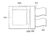
- the display device may be incorporated into an electronic apparatus according to each application example described later, for example, as a module as illustrated in FIG.
- a display unit 920 and drive circuits 930A and 930B are formed on a substrate 910.
- an external connection terminal (not shown) for connecting the drive circuit 930 and an external device is formed.
- a flexible printed circuit board (FPC) 950 for signal input / output is connected to the external connection terminal.
- the display unit 920 includes the display unit 10, and the drive circuits 930 ⁇ / b> A and 930 ⁇ / b> B include all or part of the drive units 20 and 40.
- FIG. 19 illustrates an appearance of a television device.
- This television device has a main body 110 and a display unit 120, and the display unit 120 is constituted by the display device described above.
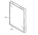
- FIG. 20A shows the appearance of an electronic book
- FIG. 20B shows the appearance of another electronic book.
- Each of these electronic books has, for example, a main body 210 and a display unit 220, and the display unit 220 is configured by the display device described above.
- FIG. 21 shows the appearance of a smartphone.
- This smartphone has, for example, a main body part 310 and a display part 320, and the display part 320 is constituted by the display device described above.
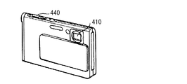
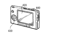
- FIG. 22A and 22B show the appearance of the digital camera
- FIG. 22A shows the appearance of the digital camera viewed from the front (subject side)
- FIG. 22B shows the digital camera behind the image (image side).
- the digital camera includes, for example, a flash light emitting unit 410, a display unit 420, a menu switch 430, and a shutter button 440
- the display unit 420 is configured by the display device described above.
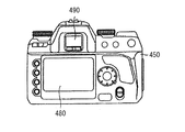
- FIGS. 23A and 23B show the appearance of a single-lens reflex digital camera with interchangeable lenses.
- FIG. 23A shows the appearance of the digital camera viewed from the front (subject side), and FIG. The appearance of the digital camera viewed from behind (image side) is shown.
- the digital camera includes, for example, a main body (camera body) 450, an interchangeable photographing lens unit (interchangeable lens) 460, a grip 470, a monitor 480, and a viewfinder 490. It is comprised by the display apparatus.
- FIG. 24 shows the appearance of a notebook personal computer.
- This notebook personal computer has, for example, a main body 510, a keyboard 520, and a display 530, and the display 530 is constituted by the display device described above.
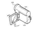
- FIG. 25 shows the appearance of the video camera.
- the video camera includes, for example, a main body 610, a lens 620, a start / stop switch 630, and a display unit 640, and the display unit 640 includes the display device described above.
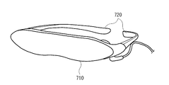
- FIG. 26 shows the appearance of the head mounted display.
- the head-mounted display has, for example, a glasses-shaped display unit 710 and an ear hook unit 720, and the display unit 710 is configured by the display device described above.
- the present technology has been described above with some embodiments and modifications, and application examples to electronic devices. However, the present technology is not limited to these embodiments and the like, and various modifications are possible. is there. According to the present technology, for example, a panel with a narrow frame region can be realized, so that the degree of freedom in product design of electronic devices can be increased.
- the capacitive element Csub is provided in the sub-pixel 11.
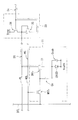
- the present invention is not limited to this, and instead, for example, as shown in the sub-pixel 11D shown in FIG.
- the element Csub may not be provided. That is, in this example, the sub-pixel 11D has a so-called “2Tr1C” configuration including two transistors (the write transistor WSTr and the drive transistor DRTr) and one capacitor element Cs.
- a unit pixel (1) a unit pixel; A switch that performs on / off control between a second terminal to which a DC signal is applied and a third terminal connected to the unit pixel, based on a pulse signal applied to the first terminal; A display device comprising: a non-linear element inserted between the first terminal and the third terminal.
- the nonlinear element is a first transistor having a drain and a gate connected to the third terminal, and a source connected to the first terminal;
- a first wiring that is connected to the first terminal and transmits the pulse signal
- the display device further including: a second wiring that is connected to the second terminal and intersects the first wiring and transmits the DC signal.
- the pulse signal transitions between a first voltage that turns on the switch and turns off the nonlinear element and a second voltage that turns off the switch.
- the display device according to any one of (1) to (6).
- the unit pixel includes a display element and a driving transistor that supplies a driving current to the display element.
- the unit pixel further includes a first capacitor element and a write transistor,
- the drive transistor has a gate, a source connected to the display element, and a drain connected to the third terminal,
- the first capacitive element is inserted between a gate and a source of the driving transistor,
- the write transistor applies a reset voltage during a write preparation period and a pixel voltage during a write period to the gate of the drive transistor by being turned on. Display device.
- the writing preparation period includes a first sub period and a second sub period arranged after the first sub period,
- the pulse signal is The second voltage in the first sub-period;
- the nonlinear element applies a third voltage corresponding to the second voltage to the unit pixel
- the display device according to (10) wherein in the second sub period and the writing period, the switch applies a fourth voltage indicated by the DC signal to the unit pixel.
- the nonlinear element sets the source voltage of the driving transistor to the third voltage via the driving transistor
- the write preparation period includes a third sub-period arranged before the first sub-period,
- the pulse signal is the first voltage in the third sub-period;
- the display device according to any one of (10) to (12), wherein the switch applies a fourth voltage indicated by the DC signal to the unit pixel in the third sub-period.
- the unit pixel further includes a first capacitor element and a control transistor,
- the drive transistor has a gate, a source connected to the display element, and a drain connected to the third terminal,
- the first capacitive element is inserted between a gate and a source of the driving transistor,
- the control transistor is turned on, with respect to the gate of the drive transistor, in one or more sub-periods of a plurality of sub-periods included in the write preparation period arranged before the write period.
- a drive device comprising: a non-linear element inserted between the first terminal and the third terminal.
- a display device and a control unit that performs operation control on the display device;
- the display device A unit pixel;
- a switch that performs on / off control between a second terminal to which a DC signal is applied and a third terminal connected to the unit pixel, based on a pulse signal applied to the first terminal;
- An electronic device comprising: a non-linear element inserted between the first terminal and the third terminal.
Landscapes
- Engineering & Computer Science (AREA)
- Physics & Mathematics (AREA)
- Computer Hardware Design (AREA)
- General Physics & Mathematics (AREA)
- Theoretical Computer Science (AREA)
- Control Of El Displays (AREA)
- Control Of Indicators Other Than Cathode Ray Tubes (AREA)
- Electroluminescent Light Sources (AREA)
Abstract
Description
1.第1の実施の形態
2.第2の実施の形態
3.適用例
[構成例]
図1は、第1の実施の形態に係る表示装置の一構成例を表すものである。表示装置1は、有機EL素子を用いた、アクティブマトリックス方式の表示装置である。なお、本開示の実施の形態に係る駆動装置、駆動方法は、本実施の形態により具現化されるので、併せて説明する。この表示装置1は、表示部10および駆動部20を備えている。
続いて、本実施の形態の表示装置1の動作および作用について説明する。
まず、図1を参照して、表示装置1の全体動作概要を説明する。映像信号処理部21は、外部から供給される映像信号Sdispに対して所定の信号処理を行い、映像信号Sdisp2を生成する。タイミング生成部22は、外部から供給される同期信号Ssyncに基づいて、走査線駆動部23、電源線駆動部26およびデータ線駆動部27に対してそれぞれ制御信号を供給し、これらがお互いに同期して動作するように制御する。走査線駆動部23は、タイミング生成部22から供給された制御信号に従って、複数の走査線WSLに対して走査信号WSを順次印加することにより、行ごとにサブ画素11を順次選択する。電源線駆動部26は、タイミング生成部22から供給された制御信号に従って、複数の電源線PLに対して電源信号DSを順次印加することにより、行ごとにサブ画素11の発光動作および消光動作の制御を行う。データ線駆動部27は、映像信号処理部21から供給された映像信号Sdisp2およびタイミング生成部22から供給された制御信号に従って、各サブ画素11の発光輝度を指示する画素電圧Vsig、およびVth補正を行うための電圧Vofsを含む信号Sigを生成し、各データ線DTLに印加する。表示部10は、駆動部20から供給された走査信号WS、電源信号DS、および信号Sigに基づいて、表示を行う。
図6は、駆動部20の動作のタイミング図を表すものであり、(A)は走査信号WSの波形を示し、(B)は電源信号DSの波形を示し、(C)は信号Sigの波形を示す。図6(A)において、走査信号WS(k)は、kライン目のサブ画素11を駆動する走査信号WSであり、同様に、走査信号WS(k+1),WS(k+2),WS(K+3)は、それぞれ、(k+1)ライン目、(k+2)ライン目、(k+3)ライン目のサブ画素11を駆動する走査信号WSである。電源信号DS(図6(B))についても同様である。
次に、駆動回路33の詳細動作について説明する。駆動回路33は、電圧生成部31から供給された電圧Vccp、およびシフトレジスタ32から供給された走査信号Ssに基づいて、電源信号DSを生成する。
次に、比較例に係る電源線駆動部26Rについて説明する。本比較例は、電圧生成部31Rが電圧Vccp,Viniを生成し、駆動回路33Rが電圧Vccp,Viniのうちの一方を選択して出力するものである。その他の構成は、本実施の形態(図1)と同様である。
以上のように本実施の形態では、スイッチとして機能するトランジスタと、非線形素子(ダイオード)として機能するトランジスタを用いて駆動回路を構成したので、電源線駆動部の構成をシンプルにすることができる。これにより、回路規模を小さくすることができ、回路および配線の配置面積を小さくすることができ、回路レイアウトの自由度を高めることができるとともに、表示装置全体としての商品デザインの自由度を高めることができる。
上記実施の形態では、駆動回路33において、ダイオード接続されたトランジスタ35を設けたが、これに限定されるものではなく、これに代えて、例えば、図11に示したように、ダイオード35Bを設けてもよい。この電源線駆動部26Bは、駆動回路33Bを有している。駆動回路33B(k)では、ダイオード35Bのアノードは電源線PL(k)に接続され、カソードは配線L2(k)に接続されている。
上記実施の形態では、駆動回路のトランジスタ34,35をNチャネルMOS型のTFTにより構成したが、これに限定されるものではなく、例えば、図12に示したように、PチャンネルMOS型のTFTにより構成してもよい。この変形例に係る電源線駆動部26Cは、駆動回路33Cと、電圧生成部31Cと、シフトレジスタ32Cとを有している。駆動回路33Cは、トランジスタ36,37を有している。トランジスタ36,37は、PチャンネルMOS型のTFTである。トランジスタ36は、非線形素子(ダイオード)として機能するものであり、トランジスタ37は、スイッチとして機能するものである。電圧生成部31Cは、電圧Viniを生成するものである。シフトレジスタ32Cは、タイミング生成部22から供給される制御信号(図示せず)に基づいて、駆動対象となる画素ラインを選択するための複数の走査信号Ssを生成するものである。各走査信号Ssの高レベル電圧VHは、電圧Vccpよりも、駆動回路33Cのトランジスタ36の閾値電圧の絶対値|Vth|だけ高い電圧(Vccp+|Vth|)である。
上記実施の形態では、駆動回路33を用いて電源線駆動部26を構成したが、これに限定されるものではなく、これに代えて、もしくはこれに加え、例えば、駆動回路33を用いて走査線駆動部23を構成してもよい。この場合には、走査線駆動部23の構成をシンプルにすることができる。
上記実施の形態では、本技術を、有機EL素子を用いた表示装置に適用したが、これに限定されるものではなく、これに代えて、例えば、液晶表示素子を用いた表示装置に適用してもよい。具体的には、例えば、画素電圧を書き込む画素を選択する回路(上記実施の形態における走査駆動部23に相当)に適用することができる。
上記実施の形態では、図7等に示したように、Vth補正期間P2の前に、1つの初期化期間P1を設けたが、これに限定されるものではなく、これに代えて、例えば、複数の初期化期間P1を設けてもよい。この場合、複数の初期化期間P1は、例えば、複数の水平期間にわたって設けることができる。これにより、長い初期化期間P1を確保することができるため、より確実にサブ画素11の初期化を行うことができる。
次に、第2の実施の形態に係る表示装置2について説明する。本実施の形態は、サブ画素11を初期化する前に、サブ画素11に対して電圧Vofsの書込みを行うことにより、消光動作を行うものである。なお、上記第1の実施の形態に係る表示装置1と実質的に同一の構成部分には同一の符号を付し、適宜説明を省略する。
上記実施の形態では、図14等に示したように、初期化期間P1の前に、1つの消光動作期間P0を設けたが、これに限定されるものではなく、これに代えて、例えば、複数の消光動作期間P0を設けてもよい。この場合、複数の消光動作期間P0は、例えば、複数の水平期間にわたって設けることができる。これにより、長い消光動作期間P0を確保することができるため、より確実に消光動作を行うことができる。
上記実施の形態では、初期化期間P1に先立つ消光動作期間P0において、書込トランジスタWSTrを介して、駆動トランジスタDRTrのゲートに電圧Vofsを印加したが、これに限定されるものではない。例えば、図17に示すサブ画素11Aのように、制御トランジスタCTrを設け、この制御トランジスタCTrを介して、駆動トランジスタDRTrのゲートに電圧Vofsを印加してもよい。この例では、制御トランジスタCTrのドレインは、駆動トランジスタDRTrのゲートに接続され、ゲートには制御信号CTLが供給され、ソースには電圧Vofsが供給されている。そして、制御トランジスタCTrをオン状態にすることにより、駆動トランジスタDRTrのゲートに電圧Vofsが印加される。
上記実施の形態に係る表示装置2に、上記第1の実施の形態の各変形例を適用してもよい。
次に、上述した実施の形態で説明した表示装置の適用例について説明する。上記実施の形態の表示装置は、テレビジョン装置、デジタルカメラ、ノート型パーソナルコンピュータ、携帯電話等の携帯端末装置あるいはビデオカメラなど、外部から入力された映像信号あるいは内部で生成した映像信号を、画像あるいは映像として表示するあらゆる分野の電子機器の表示装置に適用することが可能である。
図19は、テレビジョン装置の外観を表すものである。このテレビジョン装置は、本体部110および表示部120を有しており、表示部120が、上記の表示装置により構成されている。
図20Aは、電子ブックの外観を表すものであり、図20Bは、他の電子ブックの外観を表したものである。これらの電子ブックは、いずれも、例えば本体部210および表示部220を有しており、表示部220が上記の表示装置により構成されている。
図21は、スマートフォンの外観を表すものである。このスマートフォンは、例えば、本体部310および表示部320を有しており、表示部320が上記の表示装置により構成されている。
図22A,22Bは、デジタルカメラの外観を表すものであり、図22Aは、そのデジタルカメラをその前方(被写体側)から眺めた外観を示し、図22Bは、そのデジタルカメラをその後方(像側)から眺めた外観を示す。このデジタルカメラは、例えば、フラッシュ用の発光部410、表示部420、メニュースイッチ430、およびシャッターボタン440を有しており、表示部420が上記の表示装置により構成されている。
図23A,23Bは、レンズ交換式一眼レフレックスタイプのデジタルカメラの外観を表すものであり、図23Aは、そのデジタルカメラをその前方(被写体側)から眺めた外観を示し、図23Bは、そのデジタルカメラをその後方(像側)から眺めた外観を示す。このデジタルカメラは、例えば、本体部(カメラボディ)450、交換式の撮影レンズユニット(交換レンズ)460、グリップ部470、モニタ480、およびビューファインダ490を有しており、ビューファインダ490が上記の表示装置により構成されている。
図24は、ノート型パーソナルコンピュータの外観を表したものである。このノート型パーソナルコンピュータは、例えば、本体部510、キーボード520、および表示部530を有しており、表示部530が上記の表示装置により構成されている。
図25は、ビデオカメラの外観を表したものである。このビデオカメラは、例えば、本体部610、レンズ620、スタート/ストップスイッチ630、および表示部640を有しており、表示部640が上記の表示装置により構成されている。
図26は、ヘッドマウントディスプレイの外観を表したものである。このヘッドマウントディスプレイは、例えば、眼鏡形の表示部710および耳掛け部720を有しており、表示部710が上記の表示装置により構成されている。
第1の端子に印加されたパルス信号に基づいて、直流信号が印加された第2の端子と前記単位画素に接続された第3の端子との間をオンオフ制御するスイッチと、
前記第1の端子と前記第3の端子との間に挿設された非線形素子と
を備えた表示装置。
前記スイッチは、前記第1のトランジスタのチャネル幅よりも大きいチャネル幅を有する第2のトランジスタである
前記(1)に記載の表示装置。
前記(2)に記載の表示装置。
前記(1)に記載の表示装置。
前記第2の端子に接続されるとともに前記第1の配線と交差し、前記直流信号を伝える第2の配線と
をさらに備えた
前記(1)から(4)のいずれかに記載の表示装置。
前記(5)に記載の表示装置。
前記(1)から(6)のいずれかに記載の表示装置。
前記スイッチは、前記駆動トランジスタに前記駆動電流を供給する
前記(7)に記載の表示装置。
前記駆動トランジスタは、ゲートと、前記表示素子に接続されたソースと、前記第3の端子に接続されたドレインとを有し、
前記第1の容量素子は、前記駆動トランジスタのゲートとソースとの間に挿設され、
前記書込トランジスタは、オン状態になることにより、前記駆動トランジスタのゲートに対して、書込準備期間においてリセット電圧を印加するとともに、書込期間において画素電圧を印加する
前記(8)に記載の表示装置。
前記パルス信号は、
前記第1のサブ期間において前記第2の電圧であり、
前記第2のサブ期間および前記書込期間において前記第1の電圧である
前記(9)に記載の表示装置。
前記第2のサブ期間および前記書込期間において、前記スイッチは、前記単位画素に対して、前記直流信号が示す第4の電圧を印加する
前記(10)に記載の表示装置。
前記第2のサブ期間において、前記スイッチは、前記駆動トランジスタに電流を流すことにより、前記駆動トランジスタのソース電圧を変化させる
前記(11)に記載の表示装置。
前記パルス信号は、前記第3のサブ期間において前記第1の電圧であり、
前記スイッチは、前記第3のサブ期間において、前記単位画素に対して、前記直流信号が示す第4の電圧を印加する
前記(10)から(12)のいずれかに記載の表示装置。
前記(13)に記載の表示装置。
前記駆動トランジスタは、ゲートと、前記表示素子に接続されたソースと、前記第3の端子に接続されたドレインとを有し、
前記第1の容量素子は、前記駆動トランジスタのゲートとソースとの間に挿設され、
前記制御トランジスタは、オン状態になることにより、前記駆動トランジスタのゲートに対して、書込期間の前に配置された書込準備期間に含まれる複数のサブ期間のうちの1以上のサブ期間においてリセット電圧を印加する
前記(8)に記載の表示装置。
前記(9)から(15)のいずれかに記載の表示装置。
前記第1の端子と前記第3の端子との間に挿設された非線形素子と
を備えた駆動装置。
前記第1の端子と前記第3の端子との間で非線形動作を行う
駆動方法。
前記表示装置に対して動作制御を行う制御部と
を備え、
前記表示装置は、
単位画素と、
第1の端子に印加されたパルス信号に基づいて、直流信号が印加された第2の端子と前記単位画素に接続された第3の端子との間をオンオフ制御するスイッチと、
前記第1の端子と前記第3の端子との間に挿設された非線形素子と
を有する
電子機器。
Claims (19)
- 単位画素と、
第1の端子に印加されたパルス信号に基づいて、直流信号が印加された第2の端子と前記単位画素に接続された第3の端子との間をオンオフ制御するスイッチと、
前記第1の端子と前記第3の端子との間に挿設された非線形素子と
を備えた表示装置。 - 前記非線形性素子は、前記第3の端子に接続されたドレインおよびゲートと、前記第1の端子に接続されたソースとを有する第1のトランジスタであり、
前記スイッチは、前記第1のトランジスタのチャネル幅よりも大きいチャネル幅を有する第2のトランジスタである
請求項1に記載の表示装置。 - 前記第1のトランジスタの導電型は、前記第2のトランジスタの導電型と同じである
請求項2に記載の表示装置。 - 前記非線形素子は、前記第3の端子に接続されたアノード、および前記第1の端子に接続されたカソードを有するダイオードである
請求項1に記載の表示装置。 - 前記第1の端子に接続され、前記パルス信号を伝える第1の配線と、
前記第2の端子に接続されるとともに前記第1の配線と交差し、前記直流信号を伝える第2の配線と
をさらに備えた
請求項1に記載の表示装置。 - 前記第1の配線と前記第2の配線との交差部分において、前記第2の配線のシート抵抗は、前記第1の配線のシート抵抗よりも低い
請求項5に記載の表示装置。 - 前記パルス信号は、前記スイッチをオン状態にさせるとともに前記非線形素子をオフ状態にさせる第1の電圧と、前記スイッチをオフ状態にさせる第2の電圧との間で遷移するものである
請求項1に記載の表示装置。 - 前記単位画素は、表示素子と、前記表示素子に駆動電流を供給する駆動トランジスタとを有し、
前記スイッチは、前記駆動トランジスタに前記駆動電流を供給する
請求項7に記載の表示装置。 - 前記単位画素は、第1の容量素子と、書込トランジスタとをさらに備え、
前記駆動トランジスタは、ゲートと、前記表示素子に接続されたソースと、前記第3の端子に接続されたドレインとを有し、
前記第1の容量素子は、前記駆動トランジスタのゲートとソースとの間に挿設され、
前記書込トランジスタは、オン状態になることにより、前記駆動トランジスタのゲートに対して、書込準備期間においてリセット電圧を印加するとともに、書込期間において画素電圧を印加する
請求項8に記載の表示装置。 - 前記書込準備期間は、第1のサブ期間と、前記第1のサブ期間の後に配置された第2のサブ期間を含み、
前記パルス信号は、
前記第1のサブ期間において前記第2の電圧であり、
前記第2のサブ期間および前記書込期間において前記第1の電圧である
請求項9に記載の表示装置。 - 前記第1のサブ期間において、前記非線形素子は、前記単位画素に対して前記第2の電圧に対応する第3の電圧を印加し、
前記第2のサブ期間および前記書込期間において、前記スイッチは、前記単位画素に対して、前記直流信号が示す第4の電圧を印加する
請求項10に記載の表示装置。 - 前記第1のサブ期間において、前記非線形素子は、前記駆動トランジスタを介して、前記駆動トランジスタのソース電圧を前記第3の電圧に設定し、
前記第2のサブ期間において、前記スイッチは、前記駆動トランジスタに電流を流すことにより、前記駆動トランジスタのソース電圧を変化させる
請求項11に記載の表示装置。 - 前記書込準備期間は、前記第1のサブ期間の前に配置された第3のサブ期間を含み、
前記パルス信号は、前記第3のサブ期間において前記第1の電圧であり、
前記スイッチは、前記第3のサブ期間において、前記単位画素に対して、前記直流信号が示す第4の電圧を印加する
請求項10に記載の表示装置。 - 前記第3のサブ期間において、前記駆動トランジスタは、前記表示素子に供給する前記駆動電流の電流量を低下させる
請求項13に記載の表示装置。 - 前記単位画素は、第1の容量素子と、制御トランジスタとをさらに備え、
前記駆動トランジスタは、ゲートと、前記表示素子に接続されたソースと、前記第3の端子に接続されたドレインとを有し、
前記第1の容量素子は、前記駆動トランジスタのゲートとソースとの間に挿設され、
前記制御トランジスタは、オン状態になることにより、前記駆動トランジスタのゲートに対して、書込期間の前に配置された書込準備期間に含まれる複数のサブ期間のうちの1以上のサブ期間においてリセット電圧を印加する
請求項8に記載の表示装置。 - 前記単位画素は、前記駆動トランジスタのソースに接続された第2の容量素子をさらに備えた
請求項9に記載の表示装置。 - 第1の端子に印加されたパルス信号に基づいて、直流信号が印加された第2の端子と単位画素に接続された第3の端子との間をオンオフ制御するスイッチと、
前記第1の端子と前記第3の端子との間に挿設された非線形素子と
を備えた駆動装置。 - 第1の端子に印加されたパルス信号に基づいて、直流信号が印加された第2の端子と単位画素に接続された第3の端子との間をオンオフ制御するとともに、
前記第1の端子と前記第3の端子との間で非線形動作を行う
駆動方法。 - 表示装置と
前記表示装置に対して動作制御を行う制御部と
を備え、
前記表示装置は、
単位画素と、
第1の端子に印加されたパルス信号に基づいて、直流信号が印加された第2の端子と前記単位画素に接続された第3の端子との間をオンオフ制御するスイッチと、
前記第1の端子と前記第3の端子との間に挿設された非線形素子と
を有する
電子機器。
Priority Applications (3)
| Application Number | Priority Date | Filing Date | Title |
|---|---|---|---|
| US14/442,297 US10008151B2 (en) | 2013-01-07 | 2013-12-18 | Display unit, drive unit, driving method, and electronic apparatus |
| KR1020157014325A KR102080188B1 (ko) | 2013-01-07 | 2013-12-18 | 표시 장치, 구동 장치, 구동 방법, 및 전자 기기 |
| CN201380065410.8A CN104854650B (zh) | 2013-01-07 | 2013-12-18 | 显示单元、驱动单元、驱动方法及电子设备 |
Applications Claiming Priority (4)
| Application Number | Priority Date | Filing Date | Title |
|---|---|---|---|
| JP2013-000473 | 2013-01-07 | ||
| JP2013000473 | 2013-01-07 | ||
| JP2013239191A JP6281134B2 (ja) | 2013-01-07 | 2013-11-19 | 表示装置、駆動装置、駆動方法、および電子機器 |
| JP2013-239191 | 2013-11-19 |
Publications (1)
| Publication Number | Publication Date |
|---|---|
| WO2014106929A1 true WO2014106929A1 (ja) | 2014-07-10 |
Family
ID=51062251
Family Applications (1)
| Application Number | Title | Priority Date | Filing Date |
|---|---|---|---|
| PCT/JP2013/083962 Ceased WO2014106929A1 (ja) | 2013-01-07 | 2013-12-18 | 表示装置、駆動装置、駆動方法、および電子機器 |
Country Status (6)
| Country | Link |
|---|---|
| US (1) | US10008151B2 (ja) |
| JP (1) | JP6281134B2 (ja) |
| KR (1) | KR102080188B1 (ja) |
| CN (1) | CN104854650B (ja) |
| TW (1) | TWI569246B (ja) |
| WO (1) | WO2014106929A1 (ja) |
Families Citing this family (8)
| Publication number | Priority date | Publication date | Assignee | Title |
|---|---|---|---|---|
| KR101577909B1 (ko) * | 2014-09-05 | 2015-12-16 | 엘지디스플레이 주식회사 | 유기발광 표시장치의 열화 센싱 방법 |
| KR102585451B1 (ko) * | 2016-12-27 | 2023-10-06 | 삼성디스플레이 주식회사 | 발광 표시 장치 |
| KR102312348B1 (ko) * | 2017-06-30 | 2021-10-13 | 엘지디스플레이 주식회사 | 표시패널과 이를 이용한 전계 발광 표시장치 |
| KR102542980B1 (ko) * | 2017-11-21 | 2023-06-15 | 삼성디스플레이 주식회사 | 유기전계발광 표시장치 및 그의 구동방법 |
| CN109300436B (zh) * | 2018-09-27 | 2020-04-03 | 深圳市华星光电半导体显示技术有限公司 | Amoled像素驱动电路及驱动方法 |
| CN114467134B (zh) * | 2019-10-02 | 2024-04-09 | 夏普株式会社 | 显示装置 |
| JP7664698B2 (ja) * | 2020-12-23 | 2025-04-18 | 武漢天馬微電子有限公司 | 表示装置 |
| US12205542B2 (en) | 2021-07-30 | 2025-01-21 | Chengdu Boe Optoelectronics Technology Co., Ltd. | Pixel driving circuit and driving method thereof, and display panel |
Citations (5)
| Publication number | Priority date | Publication date | Assignee | Title |
|---|---|---|---|---|
| WO2004086344A1 (ja) * | 2003-03-26 | 2004-10-07 | Semiconductor Energy Laboratory Co. Ltd. | 表示装置及びその駆動方法 |
| JP2005031598A (ja) * | 2003-06-18 | 2005-02-03 | Semiconductor Energy Lab Co Ltd | 表示装置及びその駆動方法 |
| JP2005202372A (ja) * | 2003-12-19 | 2005-07-28 | Semiconductor Energy Lab Co Ltd | 表示装置及びその駆動方法 |
| JP2005242323A (ja) * | 2004-01-26 | 2005-09-08 | Semiconductor Energy Lab Co Ltd | 表示装置及びその駆動方法 |
| JP2008268263A (ja) * | 2007-04-16 | 2008-11-06 | Nagano Keiki Co Ltd | Led表示装置 |
Family Cites Families (6)
| Publication number | Priority date | Publication date | Assignee | Title |
|---|---|---|---|---|
| US7595775B2 (en) * | 2003-12-19 | 2009-09-29 | Semiconductor Energy Laboratory Co., Ltd. | Light emitting display device with reverse biasing circuit |
| US7268332B2 (en) * | 2004-01-26 | 2007-09-11 | Semiconductor Energy Laboratory Co., Ltd. | Display device and driving method of the same |
| JP4843203B2 (ja) * | 2004-06-30 | 2011-12-21 | グローバル・オーエルイーディー・テクノロジー・リミテッド・ライアビリティ・カンパニー | アクティブマトリクス型表示装置 |
| JP5407138B2 (ja) * | 2007-11-28 | 2014-02-05 | ソニー株式会社 | 表示装置とその製造方法および製造装置 |
| JP5151585B2 (ja) | 2008-03-18 | 2013-02-27 | ソニー株式会社 | 半導体デバイス、表示パネル及び電子機器 |
| KR101693693B1 (ko) * | 2010-08-02 | 2017-01-09 | 삼성디스플레이 주식회사 | 화소 및 이를 이용한 유기전계발광 표시장치 |
-
2013
- 2013-11-19 JP JP2013239191A patent/JP6281134B2/ja active Active
- 2013-12-17 TW TW102146760A patent/TWI569246B/zh active
- 2013-12-18 KR KR1020157014325A patent/KR102080188B1/ko active Active
- 2013-12-18 US US14/442,297 patent/US10008151B2/en active Active
- 2013-12-18 WO PCT/JP2013/083962 patent/WO2014106929A1/ja not_active Ceased
- 2013-12-18 CN CN201380065410.8A patent/CN104854650B/zh active Active
Patent Citations (5)
| Publication number | Priority date | Publication date | Assignee | Title |
|---|---|---|---|---|
| WO2004086344A1 (ja) * | 2003-03-26 | 2004-10-07 | Semiconductor Energy Laboratory Co. Ltd. | 表示装置及びその駆動方法 |
| JP2005031598A (ja) * | 2003-06-18 | 2005-02-03 | Semiconductor Energy Lab Co Ltd | 表示装置及びその駆動方法 |
| JP2005202372A (ja) * | 2003-12-19 | 2005-07-28 | Semiconductor Energy Lab Co Ltd | 表示装置及びその駆動方法 |
| JP2005242323A (ja) * | 2004-01-26 | 2005-09-08 | Semiconductor Energy Lab Co Ltd | 表示装置及びその駆動方法 |
| JP2008268263A (ja) * | 2007-04-16 | 2008-11-06 | Nagano Keiki Co Ltd | Led表示装置 |
Also Published As
| Publication number | Publication date |
|---|---|
| US10008151B2 (en) | 2018-06-26 |
| TW201428720A (zh) | 2014-07-16 |
| CN104854650B (zh) | 2017-04-12 |
| KR20150104086A (ko) | 2015-09-14 |
| CN104854650A (zh) | 2015-08-19 |
| KR102080188B1 (ko) | 2020-02-24 |
| JP6281134B2 (ja) | 2018-02-21 |
| US20150294623A1 (en) | 2015-10-15 |
| JP2014146020A (ja) | 2014-08-14 |
| TWI569246B (zh) | 2017-02-01 |
Similar Documents
| Publication | Publication Date | Title |
|---|---|---|
| JP6281134B2 (ja) | 表示装置、駆動装置、駆動方法、および電子機器 | |
| CN101572056B (zh) | 显示装置和显示装置驱动方法 | |
| CN102819996B (zh) | 像素电路、显示装置、电子装置和像素电路驱动方法 | |
| JP5939076B2 (ja) | 表示装置、駆動回路、駆動方法、および電子機器 | |
| US20120188150A1 (en) | Display device | |
| TWI444956B (zh) | 顯示裝置及電子裝置 | |
| CN103578423B (zh) | 显示装置、驱动电路和电子设备 | |
| WO2016072140A1 (ja) | 表示装置、表示装置の駆動方法、及び、電子機器 | |
| WO2016072139A1 (ja) | 表示装置、表示装置の駆動方法、及び、電子機器 | |
| US20250133832A1 (en) | Display unit and electronic apparatus | |
| JP6736276B2 (ja) | 表示パネルおよび表示装置 | |
| JP2014048485A (ja) | 表示装置及び電子機器 | |
| TWI567715B (zh) | A display device, a display driving device, a driving method of a display device, and an electronic device having a display device | |
| JP2017083609A (ja) | 表示装置、表示装置の駆動方法、表示素子、及び、電子機器 | |
| JP2017068033A (ja) | 表示素子、表示素子の駆動方法、表示装置、及び、電子機器 | |
| CN111354315B (zh) | 显示面板及显示装置、像素驱动方法 | |
| JP2012255873A (ja) | 表示装置、電子機器、及び、表示装置の駆動方法 | |
| JP2014160203A (ja) | 表示装置およびその駆動方法、並びに電子機器 | |
| WO2017056648A1 (ja) | 表示素子の駆動方法、表示装置、及び、電子機器 | |
| CN114175137A (zh) | 显示装置 | |
| US20140218270A1 (en) | Display device, driving method of display device, and electronic apparatus | |
| CN114512086A (zh) | 像素电路及其驱动方法、电子设备 | |
| JP2009186904A (ja) | 表示装置、電子機器、表示装置の駆動方法 | |
| JP2009294279A (ja) | 表示装置、表示装置の駆動方法および電子機器 |
Legal Events
| Date | Code | Title | Description |
|---|---|---|---|
| 121 | Ep: the epo has been informed by wipo that ep was designated in this application |
Ref document number: 13869951 Country of ref document: EP Kind code of ref document: A1 |
|
| WWE | Wipo information: entry into national phase |
Ref document number: 14442297 Country of ref document: US |
|
| ENP | Entry into the national phase |
Ref document number: 20157014325 Country of ref document: KR Kind code of ref document: A |
|
| NENP | Non-entry into the national phase |
Ref country code: DE |
|
| 122 | Ep: pct application non-entry in european phase |
Ref document number: 13869951 Country of ref document: EP Kind code of ref document: A1 |