JP6736276B2 - 表示パネルおよび表示装置 - Google Patents
表示パネルおよび表示装置 Download PDFInfo
- Publication number
- JP6736276B2 JP6736276B2 JP2015188062A JP2015188062A JP6736276B2 JP 6736276 B2 JP6736276 B2 JP 6736276B2 JP 2015188062 A JP2015188062 A JP 2015188062A JP 2015188062 A JP2015188062 A JP 2015188062A JP 6736276 B2 JP6736276 B2 JP 6736276B2
- Authority
- JP
- Japan
- Prior art keywords
- power supply
- pixels
- sub
- pixel
- supply line
- Prior art date
- Legal status (The legal status is an assumption and is not a legal conclusion. Google has not performed a legal analysis and makes no representation as to the accuracy of the status listed.)
- Active
Links
- 239000011159 matrix material Substances 0.000 claims description 18
- 238000000034 method Methods 0.000 claims description 9
- 230000008569 process Effects 0.000 claims description 7
- 238000005401 electroluminescence Methods 0.000 description 41
- 238000005516 engineering process Methods 0.000 description 27
- 239000010410 layer Substances 0.000 description 15
- 230000004048 modification Effects 0.000 description 15
- 238000012986 modification Methods 0.000 description 15
- 239000003990 capacitor Substances 0.000 description 12
- 238000002360 preparation method Methods 0.000 description 11
- 230000000694 effects Effects 0.000 description 10
- 239000004065 semiconductor Substances 0.000 description 8
- 230000008033 biological extinction Effects 0.000 description 7
- 230000004044 response Effects 0.000 description 6
- 230000000052 comparative effect Effects 0.000 description 5
- 101100309796 Saccharomyces cerevisiae (strain ATCC 204508 / S288c) SEC39 gene Proteins 0.000 description 4
- ATJFFYVFTNAWJD-UHFFFAOYSA-N Tin Chemical compound [Sn] ATJFFYVFTNAWJD-UHFFFAOYSA-N 0.000 description 4
- 101150013423 dsl-1 gene Proteins 0.000 description 4
- 101150010989 VCATH gene Proteins 0.000 description 3
- -1 DSL2 Proteins 0.000 description 2
- 230000008859 change Effects 0.000 description 2
- 238000007667 floating Methods 0.000 description 2
- 239000004973 liquid crystal related substance Substances 0.000 description 2
- 239000010409 thin film Substances 0.000 description 2
- 206010047571 Visual impairment Diseases 0.000 description 1
- 230000008878 coupling Effects 0.000 description 1
- 238000010168 coupling process Methods 0.000 description 1
- 238000005859 coupling reaction Methods 0.000 description 1
- 230000001771 impaired effect Effects 0.000 description 1
- 230000003287 optical effect Effects 0.000 description 1
- 239000012044 organic layer Substances 0.000 description 1
- 238000005070 sampling Methods 0.000 description 1
- 230000001360 synchronised effect Effects 0.000 description 1
Images


Classifications
-
- G—PHYSICS
- G09—EDUCATION; CRYPTOGRAPHY; DISPLAY; ADVERTISING; SEALS
- G09G—ARRANGEMENTS OR CIRCUITS FOR CONTROL OF INDICATING DEVICES USING STATIC MEANS TO PRESENT VARIABLE INFORMATION
- G09G3/00—Control arrangements or circuits, of interest only in connection with visual indicators other than cathode-ray tubes
- G09G3/20—Control arrangements or circuits, of interest only in connection with visual indicators other than cathode-ray tubes for presentation of an assembly of a number of characters, e.g. a page, by composing the assembly by combination of individual elements arranged in a matrix no fixed position being assigned to or needed to be assigned to the individual characters or partial characters
- G09G3/22—Control arrangements or circuits, of interest only in connection with visual indicators other than cathode-ray tubes for presentation of an assembly of a number of characters, e.g. a page, by composing the assembly by combination of individual elements arranged in a matrix no fixed position being assigned to or needed to be assigned to the individual characters or partial characters using controlled light sources
- G09G3/30—Control arrangements or circuits, of interest only in connection with visual indicators other than cathode-ray tubes for presentation of an assembly of a number of characters, e.g. a page, by composing the assembly by combination of individual elements arranged in a matrix no fixed position being assigned to or needed to be assigned to the individual characters or partial characters using controlled light sources using electroluminescent panels
- G09G3/32—Control arrangements or circuits, of interest only in connection with visual indicators other than cathode-ray tubes for presentation of an assembly of a number of characters, e.g. a page, by composing the assembly by combination of individual elements arranged in a matrix no fixed position being assigned to or needed to be assigned to the individual characters or partial characters using controlled light sources using electroluminescent panels semiconductive, e.g. using light-emitting diodes [LED]
- G09G3/3208—Control arrangements or circuits, of interest only in connection with visual indicators other than cathode-ray tubes for presentation of an assembly of a number of characters, e.g. a page, by composing the assembly by combination of individual elements arranged in a matrix no fixed position being assigned to or needed to be assigned to the individual characters or partial characters using controlled light sources using electroluminescent panels semiconductive, e.g. using light-emitting diodes [LED] organic, e.g. using organic light-emitting diodes [OLED]
- G09G3/3225—Control arrangements or circuits, of interest only in connection with visual indicators other than cathode-ray tubes for presentation of an assembly of a number of characters, e.g. a page, by composing the assembly by combination of individual elements arranged in a matrix no fixed position being assigned to or needed to be assigned to the individual characters or partial characters using controlled light sources using electroluminescent panels semiconductive, e.g. using light-emitting diodes [LED] organic, e.g. using organic light-emitting diodes [OLED] using an active matrix
- G09G3/3258—Control arrangements or circuits, of interest only in connection with visual indicators other than cathode-ray tubes for presentation of an assembly of a number of characters, e.g. a page, by composing the assembly by combination of individual elements arranged in a matrix no fixed position being assigned to or needed to be assigned to the individual characters or partial characters using controlled light sources using electroluminescent panels semiconductive, e.g. using light-emitting diodes [LED] organic, e.g. using organic light-emitting diodes [OLED] using an active matrix with pixel circuitry controlling the voltage across the light-emitting element
-
- G—PHYSICS
- G09—EDUCATION; CRYPTOGRAPHY; DISPLAY; ADVERTISING; SEALS
- G09G—ARRANGEMENTS OR CIRCUITS FOR CONTROL OF INDICATING DEVICES USING STATIC MEANS TO PRESENT VARIABLE INFORMATION
- G09G3/00—Control arrangements or circuits, of interest only in connection with visual indicators other than cathode-ray tubes
- G09G3/20—Control arrangements or circuits, of interest only in connection with visual indicators other than cathode-ray tubes for presentation of an assembly of a number of characters, e.g. a page, by composing the assembly by combination of individual elements arranged in a matrix no fixed position being assigned to or needed to be assigned to the individual characters or partial characters
- G09G3/22—Control arrangements or circuits, of interest only in connection with visual indicators other than cathode-ray tubes for presentation of an assembly of a number of characters, e.g. a page, by composing the assembly by combination of individual elements arranged in a matrix no fixed position being assigned to or needed to be assigned to the individual characters or partial characters using controlled light sources
- G09G3/30—Control arrangements or circuits, of interest only in connection with visual indicators other than cathode-ray tubes for presentation of an assembly of a number of characters, e.g. a page, by composing the assembly by combination of individual elements arranged in a matrix no fixed position being assigned to or needed to be assigned to the individual characters or partial characters using controlled light sources using electroluminescent panels
- G09G3/32—Control arrangements or circuits, of interest only in connection with visual indicators other than cathode-ray tubes for presentation of an assembly of a number of characters, e.g. a page, by composing the assembly by combination of individual elements arranged in a matrix no fixed position being assigned to or needed to be assigned to the individual characters or partial characters using controlled light sources using electroluminescent panels semiconductive, e.g. using light-emitting diodes [LED]
- G09G3/3208—Control arrangements or circuits, of interest only in connection with visual indicators other than cathode-ray tubes for presentation of an assembly of a number of characters, e.g. a page, by composing the assembly by combination of individual elements arranged in a matrix no fixed position being assigned to or needed to be assigned to the individual characters or partial characters using controlled light sources using electroluminescent panels semiconductive, e.g. using light-emitting diodes [LED] organic, e.g. using organic light-emitting diodes [OLED]
- G09G3/3225—Control arrangements or circuits, of interest only in connection with visual indicators other than cathode-ray tubes for presentation of an assembly of a number of characters, e.g. a page, by composing the assembly by combination of individual elements arranged in a matrix no fixed position being assigned to or needed to be assigned to the individual characters or partial characters using controlled light sources using electroluminescent panels semiconductive, e.g. using light-emitting diodes [LED] organic, e.g. using organic light-emitting diodes [OLED] using an active matrix
- G09G3/3233—Control arrangements or circuits, of interest only in connection with visual indicators other than cathode-ray tubes for presentation of an assembly of a number of characters, e.g. a page, by composing the assembly by combination of individual elements arranged in a matrix no fixed position being assigned to or needed to be assigned to the individual characters or partial characters using controlled light sources using electroluminescent panels semiconductive, e.g. using light-emitting diodes [LED] organic, e.g. using organic light-emitting diodes [OLED] using an active matrix with pixel circuitry controlling the current through the light-emitting element
-
- G—PHYSICS
- G09—EDUCATION; CRYPTOGRAPHY; DISPLAY; ADVERTISING; SEALS
- G09G—ARRANGEMENTS OR CIRCUITS FOR CONTROL OF INDICATING DEVICES USING STATIC MEANS TO PRESENT VARIABLE INFORMATION
- G09G3/00—Control arrangements or circuits, of interest only in connection with visual indicators other than cathode-ray tubes
- G09G3/20—Control arrangements or circuits, of interest only in connection with visual indicators other than cathode-ray tubes for presentation of an assembly of a number of characters, e.g. a page, by composing the assembly by combination of individual elements arranged in a matrix no fixed position being assigned to or needed to be assigned to the individual characters or partial characters
- G09G3/22—Control arrangements or circuits, of interest only in connection with visual indicators other than cathode-ray tubes for presentation of an assembly of a number of characters, e.g. a page, by composing the assembly by combination of individual elements arranged in a matrix no fixed position being assigned to or needed to be assigned to the individual characters or partial characters using controlled light sources
- G09G3/30—Control arrangements or circuits, of interest only in connection with visual indicators other than cathode-ray tubes for presentation of an assembly of a number of characters, e.g. a page, by composing the assembly by combination of individual elements arranged in a matrix no fixed position being assigned to or needed to be assigned to the individual characters or partial characters using controlled light sources using electroluminescent panels
- G09G3/32—Control arrangements or circuits, of interest only in connection with visual indicators other than cathode-ray tubes for presentation of an assembly of a number of characters, e.g. a page, by composing the assembly by combination of individual elements arranged in a matrix no fixed position being assigned to or needed to be assigned to the individual characters or partial characters using controlled light sources using electroluminescent panels semiconductive, e.g. using light-emitting diodes [LED]
- G09G3/3208—Control arrangements or circuits, of interest only in connection with visual indicators other than cathode-ray tubes for presentation of an assembly of a number of characters, e.g. a page, by composing the assembly by combination of individual elements arranged in a matrix no fixed position being assigned to or needed to be assigned to the individual characters or partial characters using controlled light sources using electroluminescent panels semiconductive, e.g. using light-emitting diodes [LED] organic, e.g. using organic light-emitting diodes [OLED]
- G09G3/3266—Details of drivers for scan electrodes
-
- G—PHYSICS
- G09—EDUCATION; CRYPTOGRAPHY; DISPLAY; ADVERTISING; SEALS
- G09G—ARRANGEMENTS OR CIRCUITS FOR CONTROL OF INDICATING DEVICES USING STATIC MEANS TO PRESENT VARIABLE INFORMATION
- G09G2300/00—Aspects of the constitution of display devices
- G09G2300/04—Structural and physical details of display devices
- G09G2300/0421—Structural details of the set of electrodes
- G09G2300/0426—Layout of electrodes and connections
-
- G—PHYSICS
- G09—EDUCATION; CRYPTOGRAPHY; DISPLAY; ADVERTISING; SEALS
- G09G—ARRANGEMENTS OR CIRCUITS FOR CONTROL OF INDICATING DEVICES USING STATIC MEANS TO PRESENT VARIABLE INFORMATION
- G09G2300/00—Aspects of the constitution of display devices
- G09G2300/04—Structural and physical details of display devices
- G09G2300/0421—Structural details of the set of electrodes
- G09G2300/043—Compensation electrodes or other additional electrodes in matrix displays related to distortions or compensation signals, e.g. for modifying TFT threshold voltage in column driver
-
- G—PHYSICS
- G09—EDUCATION; CRYPTOGRAPHY; DISPLAY; ADVERTISING; SEALS
- G09G—ARRANGEMENTS OR CIRCUITS FOR CONTROL OF INDICATING DEVICES USING STATIC MEANS TO PRESENT VARIABLE INFORMATION
- G09G2300/00—Aspects of the constitution of display devices
- G09G2300/04—Structural and physical details of display devices
- G09G2300/0439—Pixel structures
- G09G2300/0452—Details of colour pixel setup, e.g. pixel composed of a red, a blue and two green components
-
- G—PHYSICS
- G09—EDUCATION; CRYPTOGRAPHY; DISPLAY; ADVERTISING; SEALS
- G09G—ARRANGEMENTS OR CIRCUITS FOR CONTROL OF INDICATING DEVICES USING STATIC MEANS TO PRESENT VARIABLE INFORMATION
- G09G2300/00—Aspects of the constitution of display devices
- G09G2300/08—Active matrix structure, i.e. with use of active elements, inclusive of non-linear two terminal elements, in the pixels together with light emitting or modulating elements
- G09G2300/0809—Several active elements per pixel in active matrix panels
- G09G2300/0842—Several active elements per pixel in active matrix panels forming a memory circuit, e.g. a dynamic memory with one capacitor
-
- G—PHYSICS
- G09—EDUCATION; CRYPTOGRAPHY; DISPLAY; ADVERTISING; SEALS
- G09G—ARRANGEMENTS OR CIRCUITS FOR CONTROL OF INDICATING DEVICES USING STATIC MEANS TO PRESENT VARIABLE INFORMATION
- G09G2320/00—Control of display operating conditions
- G09G2320/02—Improving the quality of display appearance
- G09G2320/0233—Improving the luminance or brightness uniformity across the screen
-
- G—PHYSICS
- G09—EDUCATION; CRYPTOGRAPHY; DISPLAY; ADVERTISING; SEALS
- G09G—ARRANGEMENTS OR CIRCUITS FOR CONTROL OF INDICATING DEVICES USING STATIC MEANS TO PRESENT VARIABLE INFORMATION
- G09G2320/00—Control of display operating conditions
- G09G2320/02—Improving the quality of display appearance
- G09G2320/0247—Flicker reduction other than flicker reduction circuits used for single beam cathode-ray tubes
Landscapes
- Engineering & Computer Science (AREA)
- Physics & Mathematics (AREA)
- Computer Hardware Design (AREA)
- General Physics & Mathematics (AREA)
- Theoretical Computer Science (AREA)
- Control Of El Displays (AREA)
- Electroluminescent Light Sources (AREA)
- Control Of Indicators Other Than Cathode Ray Tubes (AREA)
- Devices For Indicating Variable Information By Combining Individual Elements (AREA)
Description
本技術の第2の表示パネルは、行列状に配置された複数の画素と、列方向に延在する複数の信号線および複数の電源線とを備えている。複数の電源線は、奇数番目の各画素行に割り当てられた複数の第1電源線と、偶数番目の各画素行に割り当てられた複数の第2電源線とにより構成されている。各第1電源線は互いに電気的に接続されており、各第2電源線は互いに電気的に接続されている。各画素は、複数のサブ画素で構成されている。複数の第1電源線と、複数の第2電源線とは、行方向に1または2つのサブ画素ごとに交互に配置されている。奇数番目の各画素行において互いに隣接する2つのサブ画素ごとに、1つの第1電源線が割り当てられ、偶数番目の各画素行において互いに隣接する2つのサブ画素ごとに、1つの第2電源線が割り当てられている。複数の第1電源線のうちの任意の第1電源線に割り当てられた2つのサブ画素を2つの第1サブ画素とし、複数の第1電源線のうち、2つの第1サブ画素に割り当てられた第1電源線に隣接する第2電源線に割り当てられた2つのサブ画素を2つの第2サブ画素としたときに、2つの第1サブ画素と2つの第2サブ画素とは、列方向において1サブ画素分だけ互い違いにずれて配置されている。
1.実施の形態(表示装置)
2.変形例(表示装置)
3.適用例(電子機器)
[構成]
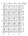
図1は、本技術の一実施の形態に係る表示装置1の概略構成を表したものである。表示装置1は、例えば、表示パネル10、コントローラ20およびドライバ30を備えている。ドライバ30は、表示パネル10の外縁部分に実装されている。表示パネル10が、本技術の「表示パネル」の一具体例に対応する。コントローラ20およびドライバ30が、本技術の「駆動回路」の一具体例に対応する。表示パネル10は、行列状に配置された複数の画素11を有している。画素11が、本技術の「画素」の一具体例に対応する。コントローラ20およびドライバ30は、外部から入力された映像信号Dinおよび同期信号Tinに基づいて、表示パネル10を駆動する。
図2は、表示パネル10の回路構成の一例を表したものである。表示パネル10は、コントローラ20およびドライバ30によって各画素11がアクティブマトリクス駆動されることにより、外部から入力された映像信号Dinおよび同期信号Tinに基づく画像を表示する。表示パネル10は、行方向に延在する複数の走査線WSLと、列方向に延在する複数の信号線DTLおよび複数の電源線DSLと、行列状に配置された複数の画素11とを有している。信号線DTLが、本技術の「信号線」の一具体例に対応する。電源線DSLが、本技術の「電源線」の一具体例に対応する。
次に、コントローラ20について説明する。コントローラ20は、例えば、映像信号処理回路21、タイミング生成回路22および電源回路23を有している。映像信号処理回路21は、例えば、外部から入力されたデジタルの映像信号Dinに対して所定の補正を行い、それにより得られた映像信号に基づいて、信号電圧Vsigを生成する。映像信号処理回路21は、例えば、生成した信号電圧Vsigを水平セレクタ31に出力する。所定の補正としては、例えば、ガンマ補正や、オーバードライブ補正などが挙げられる。タイミング生成回路22は、ドライバ30内の各回路が連動して動作するように制御するものである。タイミング生成回路22は、例えば、外部から入力された同期信号Tinに応じて(同期して)、ドライバ30内の各回路に対して制御信号を出力する。
次に、表示装置1の動作(消光から発光までの動作)について説明する。本実施の形態では、有機EL素子14のI−V特性が経時変化しても、その影響を受けることなく、有機EL素子14の発光輝度を一定に保つようにするために、有機EL素子14のI−V特性の変動に対する補償動作を組み込んでいる。さらに、本実施の形態では、駆動トランジスタTr1の閾値電圧や移動度が経時変化しても、それらの影響を受けることなく、有機EL素子14の発光輝度を一定に保つようにするために、上記閾値電圧や上記移動度の変動に対する補正動作を組み込んでいる。
次に、コントローラ20およびドライバ30は、閾値補正の準備を行う。具体的には、電源線DSLaまたは電源線DSLbの電圧がVssとなっており、かつ信号線DTLの電圧がVofs1となっている間に、ライトスキャナ32は、制御信号に応じて、走査線WSLの電圧をVoffからVonに上げる(時刻T2)。すると、ゲート電圧VgがVofs1となり、ソース電圧VsがVssとなる。このとき、ゲート−ソース間電圧Vgsは、閾値電圧Vthよりも高くなっており、駆動トランジスタTr1はオンしている。その後、水平セレクタ31は、制御信号に応じて、信号線DTLの電圧をVofs1からVosf2に切り替える。すると、ゲート電圧VgがVofs1からVosf2に下がる。このとき、ソース電圧VsはVssのまま変わらないので、ゲート−ソース間電圧Vgsが、Vofs2−Vssとなり、閾値電圧Vthよりも低くなる。その結果、駆動トランジスタTr1がオフする。その後、ライトスキャナ32は、制御信号に応じて、走査線WSLの電圧をVonからVoffに下げる(時刻T3)
次に、コントローラ20およびドライバ30は、駆動トランジスタTr1の閾値補正を行う。具体的には、信号線DTLの電圧がVofs2となっており、かつ、走査線WSLの電圧がVoffとなっている間に、電源回路23は、制御信号に応じて、電源線DSLの電圧をVssからVcc2に上げる。続いて、水平セレクタ31は、制御信号に応じて、信号線DTLの電圧をVofs2からVofs1に切り替えたのち、各画素行に対応する信号電圧Vsigを順次、信号線DTLに印加する。このとき、ライトスキャナ32は、1行目の画素行に対応する信号電圧VsigのパルスP1が入力される前に、走査線WSLの電圧をVoffからVonに上げるパルスP2を走査線WSLに印加する(時刻T4)。すると、ゲート電圧VgがVofs1まで上がり、駆動トランジスタTr1がオンするので、駆動トランジスタTr1のドレイン−ソース間に電流が流れ、ソース電圧Vsが上昇する。その結果、保持容量CsがVthに充電され、ゲート−ソース間電圧VgsがVthとなる。駆動トランジスタTr1がオンしている間に、ソース電圧VsがVofs1−Vthにまで到達しない場合(閾値補正がまだ完了していない場合)には、駆動トランジスタTr1がカットオフするまで(ゲート−ソース間電圧VgsがVthになるまで)、ライトスキャナ32は、パルスP1が入力される前に、繰り返し、パルスP2を走査線WSLに印加してもよい。
閾値補正が完了した後、コントローラ20およびドライバ30は、映像信号Dinに応じた信号電圧Vsigの書き込みと、移動度補正を行う。具体的には、信号線DTLの電圧がVsigとなっており、かつ電源線DSLaまたは電源線DSLbの電圧がVcc2となっている間に、ライトスキャナ32は、制御信号に応じて、走査線WSLの電圧をVoffからVonに上げ(時刻T6)、駆動トランジスタTr1のゲートを信号線DTLに接続する。すると、ゲート電圧Vgが信号線DTLの電圧Vsigとなる。このとき、有機EL素子14のアノード電圧はこの段階ではまだ有機EL素子14の閾値電圧Velよりも小さく、有機EL素子14はカットオフしている。そのため、ゲート−ソース間の電流は有機EL素子14の素子容量Coledに流れ、素子容量Coledが充電されるので、ソース電圧VsがΔVsだけ上昇し、やがてゲート−ソース間電圧VgsがVsig+Vth−ΔVsとなる。このようにして、書き込みと同時に移動度補正が行われる。ここで、駆動トランジスタTr1の移動度が大きい程、ΔVsも大きくなるので、ゲート−ソース間電圧Vgsを発光前にΔVsだけ小さくすることにより、画素11ごとの移動度のばらつきを取り除くことができる。
各画素11において信号書込・移動度補正が完了した後、電源線33は、制御信号に応じて、電源線DSLaまたは電源線DSLbの電圧をVcc2からVcc1に上げる(時刻T8)。すると、駆動トランジスタTr1のドレイン−ソース間に電流Idsが流れ、ソース電圧Vsが上昇する。その結果、有機EL素子14に閾値電圧Vel以上の電圧が印加され、有機EL素子14が所望の輝度で発光する。
次に、比較例と対比しつつ、表示装置1の効果について説明する。
以下に、表示装置1の変形例について説明する。なお、以下では、上記実施の形態の表示装置1と共通する構成要素に対しては、同一の符号が付与される。さらに、上記実施の形態の表示装置1と共通する構成要素についての説明は、適宜、省略されるものとする。
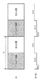
上記実施の形態では、各電源線DSLaおよび各電源線DSLbが各信号線DTLの延在方向と同一の方向に延在していた。しかし、上記実施の形態において、各電源線DSLaおよび各電源線DSLbが、各信号線DTLとは異なる層内に配置されている場合には、例えば、図13に示したように、各電源線DSLaおよび各電源線DSLbは、各信号線DTLと直交する方向(つまり、各走査線WSLの延在方向と同一の方向)に延在していてもよい。ただし、その場合には、各電源線DSLaを束ねる配線DSL1,DSL2と、各電源線DSLbを束ねる配線DSL3,DSL4とが、左右の額縁領域に必要となる。なお、各電源線DSLaにおいて、配線DSL1だけでなく、配線DSL2も必要であるのは、各電源線DSLaがパネルの長手方向(左右方向)に延在している場合には、発光電流による電圧降下を抑える必要があるためである。また、各電源線DSLbにおいて、配線DSL3だけでなく、配線DSL4も必要であるのは、各電源線DSLbがパネルの長手方向(左右方向)に延在している場合には、発光電流による電圧降下を抑える必要があるためである。このように、配線DSL1,DSL2,DSL3,DSL4が左右の額縁領域に設けられている場合には、配線DSL1,DSL2,DSL3,DSL4の分だけ、左右の額縁領域が大きくなるが、スキャナ回路が設けられている場合よりも、左右の額縁領域を狭くすることができる。
上記実施の形態では、各画素11に含まれる4つのサブ画素12は、2x2の行列に配置されていた。しかし、上記実施の形態および変形例Aにおいて、各画素11に含まれる4つのサブ画素12は、例えば、図14に示したように、1x4の行列に配置されていてもよい。
上記実施の形態では、各画素11は、4つのサブ画素12を有していた。しかし、上記実施の形態および変形例Aにおいて、各画素11は、例えば、図15に示したように、3つのサブ画素12を有していてもよい。3つのサブ画素12は、1x3の行列に配置されている。各画素11に含まれる3つのサブ画素12は、例えば、サブ画素11R,11G,11Bで構成されている。本変形例では、各サブ画素12と、複数の走査線WSL、複数の信号線DTLおよび複数の電源線DSLとの接続態様は、上記変形例Aと同様である。
以下、上記実施の形態およびその変形例(以下、「上記実施の形態等」と称する。)で説明した表示装置1の適用例について説明する。上記実施の形態の表示装置1は、テレビジョン装置、デジタルカメラ、ノート型パーソナルコンピュータ、携帯電話等の携帯端末装置あるいはビデオカメラなど、外部から入力された映像信号あるいは内部で生成した映像信号を、画像あるいは映像として表示するあらゆる分野の電子機器の表示装置に適用することが可能である。
(1)
行列状に配置された複数の画素と、
行方向に延在する複数の走査線と、
列方向に延在する複数の信号線および複数の電源線と
を備え、
複数の電源線は、
奇数番目の各画素行に割り当てられるとともに互いに電気的に接続された複数の第1電源線と、
偶数番目の各画素行に割り当てられるとともに互いに電気的に接続された複数の第2電源線と
により構成されている
表示パネル。
(2)
奇数番目の各画素行において互いに隣接する2つの前記画素ごとに、1つの前記第1電源線が割り当てられ、
偶数番目の各画素行において互いに隣接する2つの前記画素ごとに、1つの前記第2電源線が割り当てられている
(1)に記載の表示パネル。
(3)
各前記第1電源線に割り当てられた2つの前記画素と、各前記第2電源線に割り当てられた2つの前記画素とは、1画素分だけ互い違いにずれて配置されている
(2)に記載の表示パネル。
(4)
各画素は、複数のサブ画素で構成され、
奇数番目の各画素行において互いに隣接する2つの前記サブ画素ごとに、1つの前記第1電源線が割り当てられ、
偶数番目の各画素行において互いに隣接する2つの前記サブ画素ごとに、1つの前記第2電源線が割り当てられている
(1)に記載の表示パネル。
(5)
各前記第1電源線に割り当てられた2つの前記サブ画素と、各前記第2電源線に割り当てられた2つの前記サブ画素とは、1サブ画素分だけ互い違いにずれて配置されている
(4)に記載の表示パネル。
(6)
各前記電源線は、各前記信号線と同一の層内に配置されている
(1)ないし(5)のいずれか1つに記載の表示パネル。
(7)
表示パネルと、
前記表示パネルを駆動する駆動回路と
を備え、
前記表示パネルは、
行列状に配置された複数の画素と、
行方向に延在する複数の走査線と、
列方向に延在する複数の信号線および複数の電源線と
を有し、
複数の電源線は、
奇数番目の各画素行に割り当てられた複数の第1電源線と、
偶数番目の各画素行に割り当てられた複数の第2電源線と
により構成されている
表示装置。
(8)
前記駆動回路は、1F期間を前半と後半の2つの期間に分け、奇数画素行と偶数画素行とで交互に発光を行う
(7)に記載の表示装置。
(9)
前記駆動回路は、1F期間の前半に、偶数画素行に含まれる各前記画素を発光させるとともに、奇数画素行に含まれる各前記画素を消光させ、1F期間の後半に、偶数画素行に含まれる各前記画素を消光させるとともに、奇数画素行に含まれる各前記画素を発光させる
(8)に記載の表示装置。
(10)
前記駆動回路は、偶数画素行に含まれる各前記画素を消光させる期間に、偶数画素行に含まれる各前記画素に対して、補正処理を同時に行い、さらに、奇数画素行に含まれる各前記画素を消光させる期間に、奇数画素行に含まれる各前記画素に対して、前記補正処理を同時に行う
(9)に記載の表示装置。
Claims (8)
- 行列状に配置された複数の画素と、
列方向に延在する複数の信号線および複数の電源線と
を備え、
複数の電源線は、
奇数番目の各画素行に割り当てられるとともに互いに電気的に接続された複数の第1電源線と、
偶数番目の各画素行に割り当てられるとともに互いに電気的に接続された複数の第2電源線と
により構成されており、
前記複数の第1電源線と、前記複数の第2電源線とは、行方向に1または2つの前記画素ごとに交互に配置され、
奇数番目の各画素行において互いに隣接する2つの前記画素ごとに、1つの前記第1電源線が割り当てられ、
偶数番目の各画素行において互いに隣接する2つの前記画素ごとに、1つの前記第2電源線が割り当てられて、
前記複数の第1電源線のうちの任意の前記第1電源線に割り当てられた2つの前記画素を2つの第1画素とし、前記複数の第1電源線のうち、前記2つの第1画素に割り当てられた前記第1電源線に隣接する前記第2電源線に割り当てられた2つの前記画素を2つの第2画素としたときに、前記2つの第1画素と前記2つの第2画素とは、列方向において1画素分だけ互い違いにずれて配置されている
表示パネル。 - 行列状に配置された複数の画素と、
列方向に延在する複数の信号線および複数の電源線と
を備え、
複数の電源線は、
奇数番目の各画素行に割り当てられるとともに互いに電気的に接続された複数の第1電源線と、
偶数番目の各画素行に割り当てられるとともに互いに電気的に接続された複数の第2電源線と
により構成されており、
各画素は、複数のサブ画素で構成され、
前記複数の第1電源線と、前記複数の第2電源線とは、行方向に1または2つの前記サブ画素ごとに交互に配置され、
奇数番目の各画素行において互いに隣接する2つの前記サブ画素ごとに、1つの前記第1電源線が割り当てられ、
偶数番目の各画素行において互いに隣接する2つの前記サブ画素ごとに、1つの前記第2電源線が割り当てられ、
前記複数の第1電源線のうちの任意の前記第1電源線に割り当てられた2つの前記サブ画素を2つの第1サブ画素とし、前記複数の第1電源線のうち、前記2つの第1サブ画素に割り当てられた前記第1電源線に隣接する前記第2電源線に割り当てられた2つの前記サブ画素を2つの第2サブ画素としたときに、前記2つの第1サブ画素と前記2つの第2サブ画素とは、列方向において1サブ画素分だけ互い違いにずれて配置されている
表示パネル。 - 各前記電源線は、各前記信号線と同一の層内に配置されている
請求項1または請求項2に記載の表示パネル。 - 表示パネルと、
前記表示パネルを駆動する駆動回路と
を備え、
前記表示パネルは、
行列状に配置された複数の画素と、
列方向に延在する複数の信号線および複数の電源線と
を有し、
複数の電源線は、
奇数番目の各画素行に割り当てられるとともに互いに電気的に接続された複数の第1電源線と、
偶数番目の各画素行に割り当てられるとともに互いに電気的に接続された複数の第2電源線と
により構成されており、
前記複数の第1電源線と、前記複数の第2電源線とは、行方向に1または2つの前記画素ごとに交互に配置され、
奇数番目の各画素行において互いに隣接する2つの前記画素ごとに、1つの前記第1電源線が割り当てられ、
偶数番目の各画素行において互いに隣接する2つの前記画素ごとに、1つの前記第2電源線が割り当てられて、
前記複数の第1電源線のうちの任意の前記第1電源線に割り当てられた2つの前記画素を2つの第1画素とし、前記複数の第1電源線のうち、前記2つの第1画素に割り当てられた前記第1電源線に隣接する前記第2電源線に割り当てられた2つの前記画素を2つの第2画素としたときに、前記2つの第1画素と前記2つの第2画素とは、列方向において1画素分だけ互い違いにずれて配置されている
表示装置。 - 表示パネルと、
前記表示パネルを駆動する駆動回路と
を備え、
前記表示パネルは、
行列状に配置された複数の画素と、
列方向に延在する複数の信号線および複数の電源線と
を有し、
複数の電源線は、
奇数番目の各画素行に割り当てられるとともに互いに電気的に接続された複数の第1電源線と、
偶数番目の各画素行に割り当てられるとともに互いに電気的に接続された複数の第2電源線と
により構成されており、
各画素は、複数のサブ画素で構成され、
前記複数の第1電源線と、前記複数の第2電源線とは、行方向に1または2つの前記サブ画素ごとに交互に配置され、
奇数番目の各画素行において互いに隣接する2つの前記サブ画素ごとに、1つの前記第1電源線が割り当てられ、
偶数番目の各画素行において互いに隣接する2つの前記サブ画素ごとに、1つの前記第2電源線が割り当てられ、
前記複数の第1電源線のうちの任意の前記第1電源線に割り当てられた2つの前記サブ画素を2つの第1サブ画素とし、前記複数の第1電源線のうち、前記2つの第1サブ画素に割り当てられた前記第1電源線に隣接する前記第2電源線に割り当てられた2つの前記サブ画素を2つの第2サブ画素としたときに、前記2つの第1サブ画素と前記2つの第2サブ画素とは、列方向において1サブ画素分だけ互い違いにずれて配置されている
表示装置。 - 前記駆動回路は、1F期間を前半と後半の2つの期間に分け、奇数画素行と偶数画素行とで交互に発光を行う
請求項4または請求項5に記載の表示装置。 - 前記駆動回路は、1F期間の前半に、偶数画素行に含まれる各前記画素を発光させるとともに、奇数画素行に含まれる各前記画素を消光させ、1F期間の後半に、偶数画素行に含まれる各前記画素を消光させるとともに、奇数画素行に含まれる各前記画素を発光させる
請求項6に記載の表示装置。 - 前記駆動回路は、偶数画素行に含まれる各前記画素を消光させる期間に、偶数画素行に含まれる各前記画素に対して、補正処理を同時に行い、さらに、奇数画素行に含まれる各前記画素を消光させる期間に、奇数画素行に含まれる各前記画素に対して、前記補正処理を同時に行う
請求項7に記載の表示装置。
Priority Applications (2)
| Application Number | Priority Date | Filing Date | Title |
|---|---|---|---|
| JP2015188062A JP6736276B2 (ja) | 2015-09-25 | 2015-09-25 | 表示パネルおよび表示装置 |
| US15/268,839 US9984627B2 (en) | 2015-09-25 | 2016-09-19 | Display panel and display unit |
Applications Claiming Priority (1)
| Application Number | Priority Date | Filing Date | Title |
|---|---|---|---|
| JP2015188062A JP6736276B2 (ja) | 2015-09-25 | 2015-09-25 | 表示パネルおよび表示装置 |
Publications (3)
| Publication Number | Publication Date |
|---|---|
| JP2017062374A JP2017062374A (ja) | 2017-03-30 |
| JP2017062374A5 JP2017062374A5 (ja) | 2018-10-25 |
| JP6736276B2 true JP6736276B2 (ja) | 2020-08-05 |
Family
ID=58409778
Family Applications (1)
| Application Number | Title | Priority Date | Filing Date |
|---|---|---|---|
| JP2015188062A Active JP6736276B2 (ja) | 2015-09-25 | 2015-09-25 | 表示パネルおよび表示装置 |
Country Status (2)
| Country | Link |
|---|---|
| US (1) | US9984627B2 (ja) |
| JP (1) | JP6736276B2 (ja) |
Families Citing this family (6)
| Publication number | Priority date | Publication date | Assignee | Title |
|---|---|---|---|---|
| KR102636733B1 (ko) * | 2016-11-30 | 2024-02-14 | 삼성디스플레이 주식회사 | 발광 표시 장치 |
| KR20200115944A (ko) | 2019-03-29 | 2020-10-08 | 삼성디스플레이 주식회사 | 유기발광표시장치 |
| CN111369895B (zh) * | 2020-04-23 | 2022-05-13 | 上海中航光电子有限公司 | 显示面板和显示装置 |
| KR20220037909A (ko) * | 2020-09-18 | 2022-03-25 | 삼성전자주식회사 | 디스플레이 장치 및 그 제어 방법 |
| KR20220050591A (ko) * | 2020-10-16 | 2022-04-25 | 엘지디스플레이 주식회사 | 표시장치, 구동회로 및 구동방법 |
| US11689678B2 (en) * | 2021-07-06 | 2023-06-27 | Anhui Gaozhe Information Technology Co., Ltd | Double-sided synchronous scanning device and double-sided synchronous scanner |
Family Cites Families (6)
| Publication number | Priority date | Publication date | Assignee | Title |
|---|---|---|---|---|
| WO2008152847A1 (ja) * | 2007-06-12 | 2008-12-18 | Sharp Kabushiki Kaisha | 液晶表示装置、液晶表示装置の駆動方法、およびテレビジョン受像機 |
| JP2009145531A (ja) | 2007-12-13 | 2009-07-02 | Sony Corp | 表示装置、表示装置の駆動方法および電子機器 |
| JP2010060873A (ja) * | 2008-09-04 | 2010-03-18 | Sony Corp | 画像表示装置 |
| KR101812215B1 (ko) * | 2010-12-06 | 2017-12-28 | 삼성디스플레이 주식회사 | 표시 장치 |
| JP2012198406A (ja) * | 2011-03-22 | 2012-10-18 | Seiko Epson Corp | 駆動方法、制御装置、表示装置および電子機器 |
| GB2520726A (en) * | 2013-11-29 | 2015-06-03 | St Microelectronics Res & Dev | Read-out circuitry for an image sensor |
-
2015
- 2015-09-25 JP JP2015188062A patent/JP6736276B2/ja active Active
-
2016
- 2016-09-19 US US15/268,839 patent/US9984627B2/en active Active
Also Published As
| Publication number | Publication date |
|---|---|
| US9984627B2 (en) | 2018-05-29 |
| JP2017062374A (ja) | 2017-03-30 |
| US20170092197A1 (en) | 2017-03-30 |
Similar Documents
| Publication | Publication Date | Title |
|---|---|---|
| JP6736276B2 (ja) | 表示パネルおよび表示装置 | |
| KR100686335B1 (ko) | 표시장치 및 그의 구동방법 | |
| US9466250B2 (en) | Display device and electronic apparatus, and driving method of display panel | |
| CN108986735B (zh) | 显示面板的控制装置、显示装置以及显示面板的驱动方法 | |
| JP5939076B2 (ja) | 表示装置、駆動回路、駆動方法、および電子機器 | |
| JP2009169071A (ja) | 表示装置 | |
| JP2011112723A (ja) | 表示装置およびその駆動方法ならびに電子機器 | |
| JP2010008523A (ja) | 表示装置 | |
| US10056028B2 (en) | Display unit and electronic apparatus | |
| JP2009244526A (ja) | 表示装置 | |
| CN113053281A (zh) | 像素驱动电路以及包括像素驱动电路的电致发光显示装置 | |
| JP2014029423A (ja) | 表示パネル、表示装置ならびに電子機器 | |
| US11114034B2 (en) | Display device | |
| TW201435839A (zh) | 顯示器、顯示器驅動電路、顯示器驅動方法及電子設備 | |
| US20180182290A1 (en) | Display panel and display unit | |
| TWI514350B (zh) | A driving circuit, a driving method, a display device and an electronic device | |
| JP5716292B2 (ja) | 表示装置、電子機器、表示装置の駆動方法 | |
| JP2011128442A (ja) | 表示パネル、表示装置および電子機器 | |
| JP2015094773A (ja) | 表示装置および電子機器 | |
| TWI480846B (zh) | 畫素電路、顯示面板、顯示單元及電子系統 | |
| KR20110113333A (ko) | 유기발광다이오드 표시장치 및 그 구동방법 | |
| JP2015060020A (ja) | 表示装置及び電子機器 | |
| US9767724B2 (en) | Display panel, display unit, and electronic apparatus | |
| JP2012255873A (ja) | 表示装置、電子機器、及び、表示装置の駆動方法 | |
| JP5891493B2 (ja) | 表示パネルおよびその駆動方法、表示装置ならびに電子機器 |
Legal Events
| Date | Code | Title | Description |
|---|---|---|---|
| A521 | Request for written amendment filed |
Free format text: JAPANESE INTERMEDIATE CODE: A523 Effective date: 20180907 |
|
| A621 | Written request for application examination |
Free format text: JAPANESE INTERMEDIATE CODE: A621 Effective date: 20180907 |
|
| A977 | Report on retrieval |
Free format text: JAPANESE INTERMEDIATE CODE: A971007 Effective date: 20190624 |
|
| A131 | Notification of reasons for refusal |
Free format text: JAPANESE INTERMEDIATE CODE: A131 Effective date: 20190709 |
|
| A521 | Request for written amendment filed |
Free format text: JAPANESE INTERMEDIATE CODE: A523 Effective date: 20190826 |
|
| A131 | Notification of reasons for refusal |
Free format text: JAPANESE INTERMEDIATE CODE: A131 Effective date: 20200107 |
|
| A521 | Request for written amendment filed |
Free format text: JAPANESE INTERMEDIATE CODE: A523 Effective date: 20200302 |
|
| TRDD | Decision of grant or rejection written | ||
| A01 | Written decision to grant a patent or to grant a registration (utility model) |
Free format text: JAPANESE INTERMEDIATE CODE: A01 Effective date: 20200616 |
|
| A61 | First payment of annual fees (during grant procedure) |
Free format text: JAPANESE INTERMEDIATE CODE: A61 Effective date: 20200715 |
|
| R151 | Written notification of patent or utility model registration |
Ref document number: 6736276 Country of ref document: JP Free format text: JAPANESE INTERMEDIATE CODE: R151 |
|
| S303 | Written request for registration of pledge or change of pledge |
Free format text: JAPANESE INTERMEDIATE CODE: R316303 |
|
| R350 | Written notification of registration of transfer |
Free format text: JAPANESE INTERMEDIATE CODE: R350 |
|
| R250 | Receipt of annual fees |
Free format text: JAPANESE INTERMEDIATE CODE: R250 |
|
| S803 | Written request for registration of cancellation of provisional registration |
Free format text: JAPANESE INTERMEDIATE CODE: R316803 |
|
| R350 | Written notification of registration of transfer |
Free format text: JAPANESE INTERMEDIATE CODE: R350 |
|
| S111 | Request for change of ownership or part of ownership |
Free format text: JAPANESE INTERMEDIATE CODE: R313113 |