WO2014104191A1 - 荷電粒子線装置及びその欠陥分析方法 - Google Patents
荷電粒子線装置及びその欠陥分析方法 Download PDFInfo
- Publication number
- WO2014104191A1 WO2014104191A1 PCT/JP2013/084886 JP2013084886W WO2014104191A1 WO 2014104191 A1 WO2014104191 A1 WO 2014104191A1 JP 2013084886 W JP2013084886 W JP 2013084886W WO 2014104191 A1 WO2014104191 A1 WO 2014104191A1
- Authority
- WO
- WIPO (PCT)
- Prior art keywords
- defect
- analysis
- charged particle
- particle beam
- electron
- Prior art date
- Legal status (The legal status is an assumption and is not a legal conclusion. Google has not performed a legal analysis and makes no representation as to the accuracy of the status listed.)
- Ceased
Links
Images






Classifications
-
- H—ELECTRICITY
- H01—ELECTRIC ELEMENTS
- H01J—ELECTRIC DISCHARGE TUBES OR DISCHARGE LAMPS
- H01J37/00—Discharge tubes with provision for introducing objects or material to be exposed to the discharge, e.g. for the purpose of examination or processing thereof
- H01J37/26—Electron or ion microscopes; Electron or ion diffraction tubes
- H01J37/28—Electron or ion microscopes; Electron or ion diffraction tubes with scanning beams
-
- G—PHYSICS
- G01—MEASURING; TESTING
- G01N—INVESTIGATING OR ANALYSING MATERIALS BY DETERMINING THEIR CHEMICAL OR PHYSICAL PROPERTIES
- G01N23/00—Investigating or analysing materials by the use of wave or particle radiation, e.g. X-rays or neutrons, not covered by groups G01N3/00 – G01N17/00, G01N21/00 or G01N22/00
- G01N23/22—Investigating or analysing materials by the use of wave or particle radiation, e.g. X-rays or neutrons, not covered by groups G01N3/00 – G01N17/00, G01N21/00 or G01N22/00 by measuring secondary emission from the material
- G01N23/225—Investigating or analysing materials by the use of wave or particle radiation, e.g. X-rays or neutrons, not covered by groups G01N3/00 – G01N17/00, G01N21/00 or G01N22/00 by measuring secondary emission from the material using electron or ion
-
- H—ELECTRICITY
- H01—ELECTRIC ELEMENTS
- H01J—ELECTRIC DISCHARGE TUBES OR DISCHARGE LAMPS
- H01J37/00—Discharge tubes with provision for introducing objects or material to be exposed to the discharge, e.g. for the purpose of examination or processing thereof
- H01J37/02—Details
- H01J37/04—Arrangements of electrodes and associated parts for generating or controlling the discharge, e.g. electron-optical arrangement or ion-optical arrangement
- H01J37/06—Electron sources; Electron guns
-
- H—ELECTRICITY
- H01—ELECTRIC ELEMENTS
- H01J—ELECTRIC DISCHARGE TUBES OR DISCHARGE LAMPS
- H01J37/00—Discharge tubes with provision for introducing objects or material to be exposed to the discharge, e.g. for the purpose of examination or processing thereof
- H01J37/02—Details
- H01J37/04—Arrangements of electrodes and associated parts for generating or controlling the discharge, e.g. electron-optical arrangement or ion-optical arrangement
- H01J37/147—Arrangements for directing or deflecting the discharge along a desired path
- H01J37/1472—Deflecting along given lines
-
- H—ELECTRICITY
- H01—ELECTRIC ELEMENTS
- H01J—ELECTRIC DISCHARGE TUBES OR DISCHARGE LAMPS
- H01J37/00—Discharge tubes with provision for introducing objects or material to be exposed to the discharge, e.g. for the purpose of examination or processing thereof
- H01J37/02—Details
- H01J37/20—Means for supporting or positioning the object or the material; Means for adjusting diaphragms or lenses associated with the support
-
- G—PHYSICS
- G01—MEASURING; TESTING
- G01N—INVESTIGATING OR ANALYSING MATERIALS BY DETERMINING THEIR CHEMICAL OR PHYSICAL PROPERTIES
- G01N2223/00—Investigating materials by wave or particle radiation
- G01N2223/60—Specific applications or type of materials
- G01N2223/611—Specific applications or type of materials patterned objects; electronic devices
- G01N2223/6116—Specific applications or type of materials patterned objects; electronic devices semiconductor wafer
-
- G—PHYSICS
- G01—MEASURING; TESTING
- G01N—INVESTIGATING OR ANALYSING MATERIALS BY DETERMINING THEIR CHEMICAL OR PHYSICAL PROPERTIES
- G01N2223/00—Investigating materials by wave or particle radiation
- G01N2223/60—Specific applications or type of materials
- G01N2223/646—Specific applications or type of materials flaws, defects
-
- H—ELECTRICITY
- H01—ELECTRIC ELEMENTS
- H01J—ELECTRIC DISCHARGE TUBES OR DISCHARGE LAMPS
- H01J2237/00—Discharge tubes exposing object to beam, e.g. for analysis treatment, etching, imaging
- H01J2237/15—Means for deflecting or directing discharge
-
- H—ELECTRICITY
- H01—ELECTRIC ELEMENTS
- H01J—ELECTRIC DISCHARGE TUBES OR DISCHARGE LAMPS
- H01J2237/00—Discharge tubes exposing object to beam, e.g. for analysis treatment, etching, imaging
- H01J2237/20—Positioning, supporting, modifying or maintaining the physical state of objects being observed or treated
- H01J2237/2007—Holding mechanisms
-
- H—ELECTRICITY
- H01—ELECTRIC ELEMENTS
- H01J—ELECTRIC DISCHARGE TUBES OR DISCHARGE LAMPS
- H01J2237/00—Discharge tubes exposing object to beam, e.g. for analysis treatment, etching, imaging
- H01J2237/26—Electron or ion microscopes
- H01J2237/28—Scanning microscopes
- H01J2237/2803—Scanning microscopes characterised by the imaging method
- H01J2237/2806—Secondary charged particle
-
- H—ELECTRICITY
- H01—ELECTRIC ELEMENTS
- H01J—ELECTRIC DISCHARGE TUBES OR DISCHARGE LAMPS
- H01J2237/00—Discharge tubes exposing object to beam, e.g. for analysis treatment, etching, imaging
- H01J2237/26—Electron or ion microscopes
- H01J2237/28—Scanning microscopes
- H01J2237/2813—Scanning microscopes characterised by the application
- H01J2237/2817—Pattern inspection
-
- H—ELECTRICITY
- H10—SEMICONDUCTOR DEVICES; ELECTRIC SOLID-STATE DEVICES NOT OTHERWISE PROVIDED FOR
- H10P—GENERIC PROCESSES OR APPARATUS FOR THE MANUFACTURE OR TREATMENT OF DEVICES COVERED BY CLASS H10
- H10P74/00—Testing or measuring during manufacture or treatment of wafers, substrates or devices
- H10P74/20—Testing or measuring during manufacture or treatment of wafers, substrates or devices characterised by the properties tested or measured, e.g. structural or electrical properties
- H10P74/203—Structural properties, e.g. testing or measuring thicknesses, line widths, warpage, bond strengths or physical defects
Definitions
- the inspection apparatus for inspecting a substrate to be processed when performing foreign matter inspection, for example, the wafer surface is scanned with a laser and the presence or absence of scattered light is detected to obtain information on the position and number of foreign matters. Also, when performing defect inspection to detect both foreign matter and pattern abnormalities, for example, by capturing an image of a circuit pattern of a wafer with an optical magnifier and comparing it with an image of the same pattern area in the vicinity. Information on the position and number of defects is obtained.
- step 105 the analysis position in the defect area is calculated.
- An embodiment of this analysis position calculation method will be described later.
- the brightness and darkness in the SE image represents the difference in the emission efficiency of secondary electrons, there is a possibility that the ratio of the contained elements and the combination of elements is different in regions having different brightness.
- this invention is not limited to an above-described Example, Various modifications are included.
- the above-described embodiments have been described in detail for easy understanding of the present invention, and are not necessarily limited to those having all the configurations described.
- a part of the configuration of one embodiment can be replaced with the configuration of another embodiment, and the configuration of another embodiment can be added to the configuration of one embodiment.
Landscapes
- Chemical & Material Sciences (AREA)
- Analytical Chemistry (AREA)
- Physics & Mathematics (AREA)
- Health & Medical Sciences (AREA)
- Life Sciences & Earth Sciences (AREA)
- Biochemistry (AREA)
- General Health & Medical Sciences (AREA)
- General Physics & Mathematics (AREA)
- Immunology (AREA)
- Pathology (AREA)
- Analysing Materials By The Use Of Radiation (AREA)
- Testing Or Measuring Of Semiconductors Or The Like (AREA)
Abstract
Description
解析装置5は、例えば、EDX(Energy Dispersive X-ray Spectrometer)やオージェ電子分光法を用いて元素分析を行うものである。オージェ電子分光法は、電子線を対象に照射したときに対象から放出されるオージェ電子を検出し、解析する方法であり、一般によく知られた方法である。レビュー・解析装置6は、欠陥の観察と元素分析とを両方行うことができるようにした装置である。
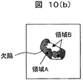
次に、SE像について、欠陥画像と参照画像の差分演算(欠陥画像と参照画像を重ね合わせて明るさの相違を算出すること)、及び閾値処理を行う。この処理により、核部分、シミ部分の両方を含む欠陥領域を抽出することができる。この抽出した領域を「領域A」とする。また、BSE像について、同様に参照画像と差分演算を行い、閾値処理を行うことにより、核部分のみの領域を抽出することができる。この抽出した領域を「領域B」とする。BSE像については、例えば、検出器の位置の異なる複数の画像を用いて、画像の演算を行うことにより欠陥領域をより感度良く抽出することができる。例えば、反射電子の検出器を、照射する一次電子ビームの光軸に点対称に2カ所配置した場合、BSE像は図5に示す陰影のついている画像に加え、図6に示すように、陰影が逆になった画像を得ることができる。この画像の差分の絶対値を算出すれば、欠陥部分の背景との差分信号は、1枚の画像を使用する場合に比較し2倍の信号量とすることができる。このように、複数のBSE像を組み合わせて演算処理を行ってもよい。
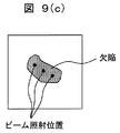
複数の点の数はユーザが指定してもよいし、何らかの条件を定めて自動で設定するようにしてもよい。
例えば、上記した実施例は本発明を分かり易く説明するために詳細に説明したものであり、必ずしも説明した全ての構成を備えるものに限定されるものではない。また、ある実施例の構成の一部を他の実施例の構成を置き換えることが可能であり、また、ある実施例の構成に他の実施例の構成を加えることも可能である。また、各実施例の構成の一部について、他の構成の追加・削除・置換をすることが可能である。
Claims (11)
- 電子ビームを出射する電子源と、該電子源から出射された前記電子ビームを収束させるコンデンサレンズと、該コンデンサレンズで収束された前記電子ビームの位置を変更する偏向手段と、該偏向手段で変更された前記電子ビームを絞って被検査対象物に照射する対物レンズと、前記被検査対象物が搭載される試料台と、前記電子ビームの照射によって前記被検査対象物の欠陥部分から放出される元素情報に基づいて欠陥を分析する欠陥分析手段とを備え、
前記欠陥分析手段は、該欠陥分析手段で1つの欠陥と判定された欠陥領域の中から、欠陥の形状に基づいて分析点を決定することを特徴とする荷電粒子線装置。 - 請求項1に記載の荷電粒子線装置において、
前記被検査対象物に前記電子ビームを照射することにより得られる二次電子を検出する二次電子検出器及び反射電子を検出する反射電子検出器と、該二次電子検出器及び反射電子検出器で検出される二次電子及び反射電子を処理して前記被検査対象物のSEM像を生成するA/D変換部とを、更に備えていることを特徴とする荷電粒子線装置。 - 請求項1に記載の荷電粒子線装置において、
前記被検査対象物は半導体ウェハであり、前記欠陥分析手段は、前記電子ビームの照射によって前記半導体ウェハの欠陥から放出される特性X線を検出し、これを電気信号に変換する特性X線検出部と、該特性X線検出部で変換された電気信号を処理して表示部へ送信する元素解析・制御部とから成ることを特徴とする荷電粒子線装置。 - 電子源から出射された電子ビームをコンデンサレンズで収束し、この収束した前記電子ビームの位置を偏向手段で変更し、この偏向した前記電子ビームを絞って試料台に搭載されている被検査対象物に対物レンズで照射し、前記電子ビームの照射によって前記被検査対象物の欠陥部分から放出される元素情報に基づいて欠陥分析手段で欠陥を分析する際に、
前記欠陥分析手段では、該欠陥分析手段で1つの欠陥と判定された欠陥領域の中から、欠陥の形状に基づいて分析点を決定することを特徴とする荷電粒子線装置の欠陥分析方法。 - 請求項4に記載の荷電粒子線装置の欠陥分析方法において、
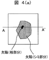
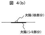
前記被検査対象物の欠陥形状を分析する際に、凸領域である核部分と平坦な領域であるシミ部分に分け、該核部分とシミ部分の代表点を分析点とすることを特徴とする荷電粒子線装置の欠陥分析方法。 - 請求項4に記載の荷電粒子線装置の欠陥分析方法において、
前記被検査対象物の欠陥形状を分析する際に、欠陥領域を複数に分割し、分割した各欠陥領域ごとに分析位置を設定することを特徴とする荷電粒子線装置の欠陥分析方法。 - 請求項4に記載の荷電粒子線装置の欠陥分析方法において、
前記被検査対象物の欠陥形状における欠陥領域の大きさが規定値以上の欠陥形状を分析する際に、前記欠陥領域内で複数の分析位置を設定することを特徴とする荷電粒子線装置の欠陥分析方法。 - 請求項7に記載の荷電粒子線装置の欠陥分析方法において、
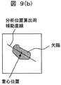
前記分析位置の設定は、前記欠陥領域の重心を通り、該欠陥領域と重複する長さが最も長くなる直線を選択し、該直線で欠陥と重複する部分で任意の点を等間隔で設定することを特徴とする荷電粒子線装置の欠陥分析方法。 - 請求項7に記載の荷電粒子線装置の欠陥分析方法において、
前記欠陥領域内での複数の分析位置の設定は、前記分析位置が、二次電子画像の明るさに応じて領域分けされた領域ごとに設定されることを特徴とする荷電粒子線装置の欠陥分析方法。 - 請求項5に記載の荷電粒子線装置の欠陥分析方法において、
前記分析位置の設定は、分割された各領域の内接円或いは多角形の中心を分析位置とすることを特徴とする荷電粒子線装置の欠陥分析方法。 - 請求項4に記載の荷電粒子線装置の欠陥分析方法において、
前記分析位置の情報として、欠陥画像に分析位置をマークした画像或いは分析座標のいずれかと、前記分析位置ごとの分析結果の両方を出力することを特徴とする荷電粒子線装置の欠陥分析方法。
Priority Applications (2)
| Application Number | Priority Date | Filing Date | Title |
|---|---|---|---|
| US14/655,081 US9312099B2 (en) | 2012-12-28 | 2013-12-26 | Charged particle beam device and method for analyzing defect therein |
| JP2014554544A JP6158226B2 (ja) | 2012-12-28 | 2013-12-26 | 荷電粒子線装置及びその欠陥分析方法 |
Applications Claiming Priority (2)
| Application Number | Priority Date | Filing Date | Title |
|---|---|---|---|
| JP2012-286843 | 2012-12-28 | ||
| JP2012286843 | 2012-12-28 |
Publications (1)
| Publication Number | Publication Date |
|---|---|
| WO2014104191A1 true WO2014104191A1 (ja) | 2014-07-03 |
Family
ID=51021265
Family Applications (1)
| Application Number | Title | Priority Date | Filing Date |
|---|---|---|---|
| PCT/JP2013/084886 Ceased WO2014104191A1 (ja) | 2012-12-28 | 2013-12-26 | 荷電粒子線装置及びその欠陥分析方法 |
Country Status (4)
| Country | Link |
|---|---|
| US (1) | US9312099B2 (ja) |
| JP (1) | JP6158226B2 (ja) |
| TW (1) | TW201432253A (ja) |
| WO (1) | WO2014104191A1 (ja) |
Cited By (2)
| Publication number | Priority date | Publication date | Assignee | Title |
|---|---|---|---|---|
| WO2016152582A1 (ja) * | 2015-03-20 | 2016-09-29 | 株式会社日立ハイテクノロジーズ | 電子線式パターン検査装置 |
| WO2021044532A1 (ja) * | 2019-09-04 | 2021-03-11 | 株式会社日立ハイテク | 荷電粒子線装置 |
Families Citing this family (9)
| Publication number | Priority date | Publication date | Assignee | Title |
|---|---|---|---|---|
| JPH0757322B2 (ja) | 1987-05-14 | 1995-06-21 | 株式会社佐竹製作所 | 摩擦切削式精穀機 |
| JP6808700B2 (ja) * | 2018-10-05 | 2021-01-06 | 日本電子株式会社 | 元素マップの生成方法および表面分析装置 |
| US20210407074A1 (en) * | 2018-11-01 | 2021-12-30 | Tokyo Electron Limited | Image processing method and image processing device |
| KR102324622B1 (ko) * | 2018-12-12 | 2021-11-12 | 어플라이드 머티리얼즈 이스라엘 리미티드 | 프로세스 모니터링 |
| US20220236194A1 (en) * | 2019-05-28 | 2022-07-28 | Nippon Telegraph And Telephone Corporation | Apparatus for Aiding Manufacturing of Optoelectronic Device |
| US10928336B1 (en) * | 2019-07-29 | 2021-02-23 | Applied Materials Israel Ltd. | X-ray based evaluation of a status of a structure of a substrate |
| WO2022091180A1 (ja) * | 2020-10-26 | 2022-05-05 | 株式会社日立ハイテク | 荷電粒子線装置 |
| JP7651706B2 (ja) * | 2021-07-28 | 2025-03-26 | 株式会社日立ハイテク | 検査装置、検査方法 |
| US12416589B2 (en) | 2022-06-24 | 2025-09-16 | SanDisk Technologies, Inc. | Systems and methods for non-destructive inspection of semiconductor devices using reflective X-ray microscope tomographic imaging |
Citations (2)
| Publication number | Priority date | Publication date | Assignee | Title |
|---|---|---|---|---|
| JP2004191187A (ja) * | 2002-12-11 | 2004-07-08 | Hitachi Ltd | 欠陥組成分析方法及び装置 |
| JP2004333210A (ja) * | 2003-05-01 | 2004-11-25 | Hitachi High-Technologies Corp | 電子線分析装置 |
Family Cites Families (9)
| Publication number | Priority date | Publication date | Assignee | Title |
|---|---|---|---|---|
| JPH09283582A (ja) | 1996-04-17 | 1997-10-31 | Fujitsu Ltd | 異物組成自動分析装置及び異物組成自動分析方法 |
| JPH10221269A (ja) | 1997-02-10 | 1998-08-21 | Advantest Corp | 異物検査装置 |
| US6407386B1 (en) * | 1999-02-23 | 2002-06-18 | Applied Materials, Inc. | System and method for automatic analysis of defect material on semiconductors |
| US7138629B2 (en) | 2003-04-22 | 2006-11-21 | Ebara Corporation | Testing apparatus using charged particles and device manufacturing method using the testing apparatus |
| JP2004363085A (ja) | 2003-05-09 | 2004-12-24 | Ebara Corp | 荷電粒子線による検査装置及びその検査装置を用いたデバイス製造方法 |
| JP2006261162A (ja) * | 2005-03-15 | 2006-09-28 | Hitachi High-Technologies Corp | レビュー装置及びレビュー装置における検査方法 |
| JP4533306B2 (ja) * | 2005-12-06 | 2010-09-01 | 株式会社日立ハイテクノロジーズ | 半導体ウェハ検査方法及び欠陥レビュー装置 |
| US7960697B2 (en) | 2008-10-23 | 2011-06-14 | Hermes-Microvision, Inc. | Electron beam apparatus |
| US8319192B2 (en) | 2010-08-24 | 2012-11-27 | Hermes Microvision Inc. | Charged particle apparatus |
-
2013
- 2013-11-05 TW TW102140091A patent/TW201432253A/zh unknown
- 2013-12-26 WO PCT/JP2013/084886 patent/WO2014104191A1/ja not_active Ceased
- 2013-12-26 US US14/655,081 patent/US9312099B2/en active Active
- 2013-12-26 JP JP2014554544A patent/JP6158226B2/ja active Active
Patent Citations (2)
| Publication number | Priority date | Publication date | Assignee | Title |
|---|---|---|---|---|
| JP2004191187A (ja) * | 2002-12-11 | 2004-07-08 | Hitachi Ltd | 欠陥組成分析方法及び装置 |
| JP2004333210A (ja) * | 2003-05-01 | 2004-11-25 | Hitachi High-Technologies Corp | 電子線分析装置 |
Cited By (11)
| Publication number | Priority date | Publication date | Assignee | Title |
|---|---|---|---|---|
| WO2016152582A1 (ja) * | 2015-03-20 | 2016-09-29 | 株式会社日立ハイテクノロジーズ | 電子線式パターン検査装置 |
| JPWO2016152582A1 (ja) * | 2015-03-20 | 2017-05-25 | 株式会社日立ハイテクノロジーズ | 電子線式パターン検査装置 |
| WO2021044532A1 (ja) * | 2019-09-04 | 2021-03-11 | 株式会社日立ハイテク | 荷電粒子線装置 |
| JPWO2021044532A1 (ja) * | 2019-09-04 | 2021-03-11 | ||
| KR20220040490A (ko) * | 2019-09-04 | 2022-03-30 | 주식회사 히타치하이테크 | 하전 입자선 장치 |
| CN114341631A (zh) * | 2019-09-04 | 2022-04-12 | 株式会社日立高新技术 | 带电粒子束装置 |
| US20220344124A1 (en) * | 2019-09-04 | 2022-10-27 | Hitachi High-Tech Corporation | Charged Particle Beam Device |
| JP7198360B2 (ja) | 2019-09-04 | 2022-12-28 | 株式会社日立ハイテク | 荷電粒子線装置 |
| KR102608709B1 (ko) | 2019-09-04 | 2023-12-04 | 주식회사 히타치하이테크 | 하전 입자선 장치 |
| US12046446B2 (en) | 2019-09-04 | 2024-07-23 | Hitachi High-Tech Corporation | Charged particle beam device |
| CN114341631B (zh) * | 2019-09-04 | 2024-12-31 | 株式会社日立高新技术 | 带电粒子束装置 |
Also Published As
| Publication number | Publication date |
|---|---|
| JP6158226B2 (ja) | 2017-07-12 |
| JPWO2014104191A1 (ja) | 2017-01-19 |
| US20150348750A1 (en) | 2015-12-03 |
| US9312099B2 (en) | 2016-04-12 |
| TW201432253A (zh) | 2014-08-16 |
Similar Documents
| Publication | Publication Date | Title |
|---|---|---|
| JP6158226B2 (ja) | 荷電粒子線装置及びその欠陥分析方法 | |
| JP4533306B2 (ja) | 半導体ウェハ検査方法及び欠陥レビュー装置 | |
| US9311697B2 (en) | Inspection method and device therefor | |
| US9390490B2 (en) | Method and device for testing defect using SEM | |
| JP3993817B2 (ja) | 欠陥組成分析方法及び装置 | |
| KR101588367B1 (ko) | 하전 입자선 장치 | |
| US7884948B2 (en) | Surface inspection tool and surface inspection method | |
| JP5118872B2 (ja) | 半導体デバイスの欠陥観察方法及びその装置 | |
| JP5164598B2 (ja) | レビュー方法、およびレビュー装置 | |
| CN106796188A (zh) | 基于自动化决策的能量分散式x射线方法及设备 | |
| JP2005259396A (ja) | 欠陥画像収集方法およびその装置 | |
| JP5608208B2 (ja) | 欠陥レビュー装置 | |
| CN101484818A (zh) | 半导体不良分析装置、不良分析方法、以及不良分析程序 | |
| JP6033325B2 (ja) | 半導体検査装置、及び荷電粒子線を用いた検査方法 | |
| JP4745380B2 (ja) | レビューsem | |
| JP5036889B2 (ja) | レビューsem | |
| JP5608209B2 (ja) | 欠陥レビュー装置 | |
| JP5163731B2 (ja) | 欠陥候補の画像表示方法 | |
| JP5190087B2 (ja) | 欠陥レビュー装置 | |
| JP2007281500A (ja) | 回路パターンの検査装置、検査システム、および検査方法 | |
| JP2005181347A (ja) | 回路パターンの検査装置、検査システム、および検査方法 | |
| JP6184922B2 (ja) | 荷電粒子ビーム装置、荷電粒子ビーム走査方法およびプログラム | |
| JP2006227026A (ja) | パターン検査方法及びパターン検査装置 | |
| US20260026296A1 (en) | Automatic creation of an imaging recipe | |
| JP2004260193A (ja) | 回路パターンの検査方法及び検査装置 |
Legal Events
| Date | Code | Title | Description |
|---|---|---|---|
| 121 | Ep: the epo has been informed by wipo that ep was designated in this application |
Ref document number: 13868717 Country of ref document: EP Kind code of ref document: A1 |
|
| ENP | Entry into the national phase |
Ref document number: 2014554544 Country of ref document: JP Kind code of ref document: A |
|
| WWE | Wipo information: entry into national phase |
Ref document number: 14655081 Country of ref document: US |
|
| NENP | Non-entry into the national phase |
Ref country code: DE |
|
| 122 | Ep: pct application non-entry in european phase |
Ref document number: 13868717 Country of ref document: EP Kind code of ref document: A1 |