WO2014103844A1 - タッチセンサシステム - Google Patents
タッチセンサシステム Download PDFInfo
- Publication number
- WO2014103844A1 WO2014103844A1 PCT/JP2013/083961 JP2013083961W WO2014103844A1 WO 2014103844 A1 WO2014103844 A1 WO 2014103844A1 JP 2013083961 W JP2013083961 W JP 2013083961W WO 2014103844 A1 WO2014103844 A1 WO 2014103844A1
- Authority
- WO
- WIPO (PCT)
- Prior art keywords
- sensor panel
- capacitance
- drive
- output
- touch sensor
- Prior art date
- Legal status (The legal status is an assumption and is not a legal conclusion. Google has not performed a legal analysis and makes no representation as to the accuracy of the status listed.)
- Ceased
Links
Images


Classifications
-
- G—PHYSICS
- G06—COMPUTING OR CALCULATING; COUNTING
- G06F—ELECTRIC DIGITAL DATA PROCESSING
- G06F3/00—Input arrangements for transferring data to be processed into a form capable of being handled by the computer; Output arrangements for transferring data from processing unit to output unit, e.g. interface arrangements
- G06F3/01—Input arrangements or combined input and output arrangements for interaction between user and computer
- G06F3/03—Arrangements for converting the position or the displacement of a member into a coded form
- G06F3/041—Digitisers, e.g. for touch screens or touch pads, characterised by the transducing means
- G06F3/044—Digitisers, e.g. for touch screens or touch pads, characterised by the transducing means by capacitive means
- G06F3/0446—Digitisers, e.g. for touch screens or touch pads, characterised by the transducing means by capacitive means using a grid-like structure of electrodes in at least two directions, e.g. using row and column electrodes
Definitions
- the present invention relates to a touch sensor system including a sensor panel and an integrated circuit that drives the sensor panel, and more particularly to a narrow frame of the sensor panel.
- Japanese Patent No. 4927216 discloses a touch sensor system including a sensor panel and an integrated circuit that controls the sensor panel.
- the sensor panel includes M drive lines and L sense lines.
- the M drive lines and the L sense lines are each connected to the integrated circuit. Therefore, in the sensor panel, each of the M drive lines and each of the L sense lines are connected to the integrated circuit outside the region where the M drive lines and the L sense lines are arranged. Wiring to be placed is arranged. As the sensor panel becomes larger, the number of drive lines and sense lines increases. As a result, the number of wirings increases. As a result, there is a problem that it is difficult to realize a narrow frame of the sensor panel.
- An object of the present invention is to provide a touch sensor system capable of realizing a narrow frame of a sensor panel.
- the touch sensor system includes a sensor panel and an integrated circuit.
- the integrated circuit controls the sensor panel.
- the integrated circuit includes a drive unit and an estimation unit.
- the estimation unit estimates the capacitance value of the first capacitance string corresponding to the k1th drive line based on the inner product operation of the output sFirst and the code sequence di, and calculates the inner product operation of the output sSecond and the code sequence di Based on the above, the capacitance value of the second capacitance string corresponding to the k2nd drive line is estimated.
- the drive unit is disposed on the sensor panel, and the estimation unit is disposed on a separately provided substrate in addition to the sensor panel.
- liquid crystal display device In the liquid crystal display device according to the embodiment of the present invention, it is possible to realize a narrow frame of the sensor panel.
- FIG. 1 is a circuit diagram illustrating a touch sensor system according to an embodiment of the present invention. It is a circuit diagram which shows the structure of the drive part shown in FIG. It is a figure for demonstrating the drive method of the sensor panel provided in the said touch sensor system. It is a timing chart for demonstrating the drive method of the said sensor panel. It is a figure for demonstrating the specific example of the orthogonal code series input into the sensor panel provided in the said touch sensor system. It is a figure for demonstrating the other specific example of the said orthogonal code sequence. It is a figure for demonstrating the other specific example of the said orthogonal code sequence.
- the touch sensor system includes a sensor panel and an integrated circuit.
- the integrated circuit controls the sensor panel.
- the integrated circuit includes a drive unit and an estimation unit.
- the estimation unit estimates the capacitance value of the first capacitance string corresponding to the k1th drive line based on the inner product operation of the output sFirst and the code sequence di, and calculates the inner product operation of the output sSecond and the code sequence di Based on the above, the capacitance value of the second capacitance string corresponding to the k2nd drive line is estimated.
- the drive unit is disposed on the sensor panel, and the estimation unit is disposed on a separately provided substrate in addition to the sensor panel.
- the drive line and the sense line are in an intersecting relationship, and therefore, among the wiring that connects the drive line and the drive unit and the wiring that connects the sense line and the estimation unit Either one needs to be routed along the outer edge of the sensor panel.
- the first configuration since the drive unit is disposed on the sensor panel, it is necessary to route the wiring connecting the drive unit and the M drive lines along the outer edge of the sensor panel. Disappear.
- the first configuration a narrower frame of the sensor panel can be realized as compared with the case where the driving unit is arranged on the substrate together with the estimation unit.
- the driving unit includes a shift register and an XOR circuit in the first configuration.
- the shift register is a cascade connection of a plurality of flip-flops.
- the XOR circuit is connected to an intermediate tap provided in the shift register. Outputs of each of the plurality of flip-flops are connected to different drive lines in the M drive lines.
- the circuit configuration of the drive unit is simplified. Therefore, it is possible to easily arrange the drive unit on the sensor panel.
- the shift register operates with a two-phase clock in the second configuration. In this case, malfunction of the shift register can be suppressed.
- FIG. 1 is a circuit diagram illustrating a configuration of a touch sensor system 1 according to an embodiment.
- the touch sensor system 1 includes a sensor panel 2 and an integrated circuit 3 that controls the sensor panel 2.
- the sensor panel 2 includes M drive lines DL1 to DLM arranged parallel to each other at a predetermined interval along the horizontal direction and a predetermined interval parallel to each other along a direction intersecting the drive lines. Arranged in a matrix of M rows ⁇ L columns between the L sense lines SL1 to SLL arranged in this manner, and the M drive lines DL1 to DLM and the L sense lines SL1 to SLL, respectively.
- the integrated circuit 3 has a drive unit 4 connected to M drive lines DL1 to DLM.
- FIG. 2 is a circuit diagram showing a configuration of the drive unit 4 of the integrated circuit 3.
- the driving unit 4 includes a shift register 20 and XOR circuits 22A to 22C.
- the shift register 20 is formed by cascading a plurality of flip-flops 24A to 24H.
- the XOR circuits 22A to 22C are connected to intermediate taps provided in the shift register 20.
- the number of XOR circuits 22A to 22C and the position of the intermediate tap in the shift register 20 are particularly limited as long as the M series signal can be generated in the drive unit 4. It is not limited.
- the number of flip-flops 24 is set to the same number as the number of drive lines DL. That is, FIG. 2 shows the drive unit 4 in the case where eight drive lines DL1 to DL8 are provided. The drive lines DL1 to DL8 connected to the flip-flops 24A to 24H are different from each other.
- a clock signal line 26 is connected to each of the plurality of flip-flops 24A to 24H. As a result, the clock signal ck flowing through the clock signal line 26 is input to each of the plurality of flip-flops 24A to 24H.
- the clock signal line 26 is connected to a clock signal generator 32 (see FIG. 1) disposed on the substrate 30.
- the clock signal generation unit 32 generates the clock signal ck.
- a reset signal line 28 is connected to each of the plurality of flip-flops 24A to 24H. As a result, the reset signal rm flowing through the reset signal line 28 is input to each of the plurality of flip-flops 24A to 24H.
- the reset signal line 28 is connected to a reset signal generator 34 (see FIG. 1) disposed on the substrate 30.
- the reset signal generator 34 generates a reset signal rm.
- the output of the flip-flop 24A is connected to the input of the flip-flop 24B and to the drive line DL2.
- the output of the flip-flop 24B is connected to the input of the flip-flop 24C, one input of the XOR circuit 22A, and the drive line DL3.
- the output of the flip-flop 24C is connected to the input of the flip-flop 24D, one input of the XOR circuit 22B, and the drive line DL4.
- the output of the flip-flop 24D is connected to the input of the flip-flop 24E, one input of the XOR circuit 22C, and the drive line DL5.
- the output of the flip-flop 24E is connected to the input of the flip-flop 24F and to the drive line DL6.
- the output of the flip-flop 24F is connected to the input of the flip-flop 24G and connected to the drive line DL for seven.
- the output of the flip-flop 24G is connected to the input of the flip-flop 24H and also connected to the drive line DL8.
- the output of the flip-flop 24H is connected to the other input of the XOR circuit 22C.
- the output of the XOR circuit 22C is connected to the other input of the XOR circuit 22B.
- the output of the XOR circuit 22B is connected to the other input of the XOR circuit 22A.
- the output of the XOR circuit 22A is connected to the input of the flip-flop 24A and to the drive line DL1.
- the flip-flops 24A to 24H are initialized every time the reset signal rm is input. Each of the flip-flops 24A to 24H outputs the input data signal every time the clock signal ck is input. As a result, in the shift register 20, every time the clock signal ck is input, the data signal input to each of the flip-flops 24A to 24G is input to the subsequent flip-flops 24B to 24H. The data signal input to the flip-flop 24H is input to the flip-flop 24A via the XOR circuits 22A to 22C.
- the data signals output from the flip-flops 24A to 24G are input not only to the subsequent flip-flops 24B to 24H but also to the drive lines DL2 to DL8.
- the data signal output from the flip-flop 24H is input not only to the flip-flop 24A via the XOR circuits 22A to 22C but also to the drive line DL1.
- the driving unit 4 can drive the M drive lines DL1 to DLM in parallel.
- FIG. 3 is a block diagram illustrating a configuration of the estimation unit 5 of the integrated circuit 3.
- the estimation unit 5 includes L analog integrators 6 connected to the L sense lines SL1 to SLL, a switch 7 connected to the L analog integrators 6, and an AD conversion connected to the switch 7.
- the analog integrator 6 includes an operational amplifier having one input grounded, an integration capacitor of a capacitor Cint disposed between the output of the operational amplifier and the other input, a transistor coupled to the other input of the operational amplifier, This transistor and another transistor connected in parallel are included.
- the integrated circuit 3 is provided with an application processing unit 11 that is connected to the inner product calculation unit 9 and executes gesture recognition processing (such as ARM) at 240 Hz.
- gesture recognition processing such as ARM
- FIG. 3 is a diagram for explaining a driving method of the sensor panel 2 provided in the touch sensor system 1.
- the code sequence di is generated when the driving unit 4 repeatedly inputs the clock signal ck to each of the flip-flops 24A to 24H.
- FIG. 4 is a timing chart for explaining a driving method of the sensor panel 2.
- the integration signal Cint of the analog integrator 6 is reset by the reset signal, and each capacitance arranged in a matrix on the sensor panel 2 is also reset.
- the reset means that the electric charge accumulated in the capacitor is discharged.
- the drive lines DL1 to DLM are driven in parallel at Vref + V or Vref ⁇ V according to +1 or ⁇ 1 which is the value of the code sequence d11, d21, d31,. Charges of ⁇ CV corresponding to the elements ⁇ 1 of the code sequence are stored.
- the analog integrator 6 reads out the signals for each sense line.
- the output sequence vector sji is And When an inner product operation di ⁇ sj of the code sequence di and the output sequence vector sj is performed, the result is as follows.
- the gain G becomes (1 / Cint).
- Cip the first capacitance column Cip
- i 1,..., M
- the output sFirst (sp1, sp2,..., SpN) from the first capacitance string is integrated by the corresponding analog integrator 6 and output from the second capacitance string.
- sSecond (sq1, sq2,..., sqN) is integrated by the analog integrator 6 provided correspondingly.
- the switch 7 sequentially switches the analog integrators 6 corresponding to the sense lines SL1 to SLL, and supplies the AD converter 8 with the output from the capacitance string integrated by each analog integrator 6.
- the output sp1 is read from the first capacitance string to the analog integrator 6 and integrated, and at the same time, the output sq1 from the second capacitance string is transferred to the other analog integrator 6.
- the switch 7 is connected to the analog integrator 6 and supplies the output sp1 read and integrated to the ADC 8.
- the switch 7 disconnects the connection with the analog integrator 6 and connects to the other analog integrator 6, and supplies the read and integrated output sq 1 to the ADC 8.
- the output sp2 is read from the first capacitance string to the analog integrator 6 and integrated.
- the output sq2 is read from the second capacitance string to the other analog integrator 6 and integrated. Is done.
- the switch 7 is connected to the analog integrator 6 and supplies the output sp2 read and integrated to the ADC 8. Next, the switch 7 releases the connection with the analog integrator 6 and connects to the other analog integrator 6, and supplies the output sq ⁇ b> 2 read and integrated to the ADC 8. In this way, the output spN and the output sqN are sequentially supplied to the ADC 8 by the analog integrator 6 and the switch 7. Further, the analog integrators 6 of all the sense lines operate in parallel with driving of the drive lines.
- the AD converter 8 performs AD conversion on the output from the capacitance string integrated by the analog integrator 6 and supplies the result to the inner product calculation unit 9.
- the inner product calculation unit 9 refers to the data stored in the RAM 10 based on the inner product calculation of the output sFirst and the code sequence di, and refers to the first static line corresponding to the k1th drive line (1 ⁇ k1 ⁇ M). A capacitance value of the capacitance string is estimated, and the second capacitance string corresponding to the k2th drive line (k1 ⁇ k2, 1 ⁇ k1 ⁇ M) based on the inner product calculation of the output sSecond and the code sequence di The capacity value of is estimated.
- the application processing unit 11 executes gesture recognition processing based on the capacitance value estimated by the inner product calculation unit 9, and generates a gesture command.
- FIG. 5 is a diagram for explaining a specific example of orthogonal code sequences input to the sensor panel.
- Specific examples of the orthogonal code sequence di having the length N include the following code sequences.
- a Hadamard matrix that is a typical orthogonal code sequence is generated by the sylvester method shown in FIG.
- a basic structure a basic unit of 2 rows ⁇ 2 columns is made.
- the upper right, upper left, and lower left bits of the basic unit are the same, and the lower right is an inversion of these bits.
- the above-mentioned 2 ⁇ 2 basic elements are synthesized as four blocks in the upper right, upper left, lower right, and lower left to create a code of a 4 ⁇ 4 bit array.
- the lower right block is bit-inverted.
- the code of the bit arrangement of 8 rows ⁇ 8 columns and 16 rows ⁇ 16 columns is generated in the same procedure.
- the codes of the 16 rows ⁇ 16 columns bit array shown in FIG. 4 can be used as orthogonal code sequences.
- the Hadamard matrix refers to a square matrix whose elements are either 1 or ⁇ 1 and whose rows are orthogonal to each other. That is, any two rows of the Hadamard matrix represent vectors that are perpendicular to each other.
- a matrix obtained by arbitrarily extracting M rows from the Nth-order Hadamard matrix can be used (where M ⁇ N).
- M ⁇ N a Hadamard matrix by a method other than the Sylvester method can also be applied to the present invention.
- FIG. 6 is a diagram for explaining another specific example of the orthogonal code sequence
- FIG. 7 is a diagram for explaining still another specific example of the orthogonal code sequence.
- Hadamard matrices obtained by methods other than these Sylvester methods can also be used as orthogonal code sequences according to the present embodiment.
- (1) First, the inner product matrix stored in the RAM 10 (FIG. 2) of the estimation unit 5 is reset to C′ij 0.
- the L output voltages sjk read at time tk respectively read by the corresponding L analog integrators 6 are supplied to the AD converter 8 in order by the switch 7 to perform AD conversion, and the AD converter 8
- the output voltage sjk at time tk that has been subjected to AD conversion by the above is supplied to the inner product calculation unit 9.
- the output voltage sjk at time tk supplied to the inner product calculation unit 9 is It becomes.
- the time is incremented (tk + 1) and the process returns to (1) until N times of processing corresponding to the length of the code sequence are performed. When the above processing is completed, the value of C′ij becomes the inner product calculation result.
- the drive unit 4 is disposed on the sensor panel 2, and the estimation unit 5 is disposed on the substrate 30 provided separately from the sensor panel 2. Therefore, compared with the case where the drive part 4 is arrange
- the M drive lines DL1 to DLM and the L sense lines SL1 to SLL intersect each other. Therefore, when the drive unit 4 is arranged on the substrate 30 together with the estimation unit 5, the wirings connecting the M drive lines DL1 to DLM and the drive unit 4 and the L sense lines SL1 to SLL and the estimation unit 5 It is necessary to route any of the wirings connecting the two along the outer edge of the sensor panel 2. On the other hand, in the present embodiment, since the drive unit 4 is disposed on the sensor panel 2, it is not necessary to route the wiring connecting the drive unit 4 and the M drive lines DL1 to DLM along the outer edge of the sensor panel 2. . As a result, in the present embodiment, it is possible to realize a narrow frame of the sensor panel 2 as compared with the case where the drive unit 4 is disposed on the substrate 30 together with the estimation unit 5.
- the drive unit 4 includes a shift register 20 and XOR circuits 22A to 22C. Therefore, the circuit configuration of the drive unit 4 is simplified. As a result, the drive unit 4 can be easily arranged on the sensor panel 2.
- the shift register 20 may operate with a two-phase clock. In this case, malfunction of the drive unit 4 can be suppressed.
Landscapes
- Engineering & Computer Science (AREA)
- General Engineering & Computer Science (AREA)
- Theoretical Computer Science (AREA)
- Human Computer Interaction (AREA)
- Physics & Mathematics (AREA)
- General Physics & Mathematics (AREA)
- Position Input By Displaying (AREA)
Abstract
センサパネルと、センサパネルを駆動する集積回路とを備えるタッチセンサシステムにおいて、センサパネルの狭額縁化を実現する。センサパネルと、センサパネルを制御する集積回路とを備える。センサパネルは、M本のドライブラインと1本のセンスラインの間に形成される第1の静電容量列、及び、上記M本のドライブラインと他の1本のセンスラインの間に形成される第2の静電容量列とを備える。集積回路は、駆動部と、推定部とを有する。駆動部は、第1の静電容量列及び第2の静電容量列のそれぞれに対して、各要素が+1または-1によって構成される長さNの直交する符号系列に基づいて、M本のドライブラインを並列に駆動して、第1の静電容量列からの出力及び第2の静電容量列からの出力をアナログ積分器に出力する。駆動部がセンサパネルに配置される。
Description
本発明は、センサパネルと、センサパネルを駆動する集積回路とを備えるタッチセンサシステムに関し、詳しくは、センサパネルの狭額縁化に関する。
従来から、タッチ位置を検出するタッチセンサシステムが知られている。例えば、特許第4927216号公報には、センサパネルと、このセンサパネルを制御する集積回路とを備えるタッチセンサシステムが開示されている。
上記公報に記載のタッチセンサシステムにおいては、センサパネルがM本のドライブラインとL本のセンスラインとを備える。M本のドライブライン及びL本のセンスラインは、それぞれ、集積回路に接続される。そのため、センサパネルにおいて、M本のドライブラインとL本のセンスラインとが配置される領域の外側には、M本のドライブラインのそれぞれと、L本のセンスラインのそれぞれとを集積回路に接続する配線が配置される。センサパネルが大型になると、ドライブライン及びセンスラインの本数が増える。そのため、上記配線の本数も増える。その結果、センサパネルの狭額縁化を実現し難いという問題があった。
本発明の目的は、センサパネルの狭額縁化を実現できるタッチセンサシステムを提供することである。
本発明の実施の形態によるタッチセンサシステムは、センサパネルと、集積回路とを備える。センサパネルは、M本のドライブラインと1本のセンスラインの間に形成される第1の静電容量列Ci1(i=1、…、M)、及び、上記M本のドライブラインと他の1本のセンスラインの間に形成される第2の静電容量列Ci2(i=1、…、M)とを備える。集積回路は、センサパネルを制御する。集積回路は、駆動部と、推定部とを有する。駆動部は、第1の静電容量列Ci1(i=1、…、M)、及び第2の静電容量列Ci2(i=1、…、M)のそれぞれに対して、各要素が+1または-1によって構成される長さNの直交する符号系列di=(di1、di2、…、diN)(i=1、…、M、及びM<N)に基づいて、M本のドライブラインを並列に駆動して、第1の静電容量列からの出力sFirst=(s11、s12、…、s1N)、及び、第2の静電容量列からの出力sSecond=(s21、s22、…、s2N)をアナログ積分器に出力する。推定部は、出力sFirstと符号系列diとの内積演算に基づいて、k1番目のドライブラインに対応する第1の静電容量列の容量値を推定し、出力sSecondと符号系列diとの内積演算に基づいて、k2番目のドライブラインに対応する第2の静電容量列の容量値を推定する。駆動部がセンサパネルに配置され、推定部がセンサパネルの他に別途設けられた基板に配置される。
本発明の実施の形態による液晶表示装置においては、センサパネルの狭額縁化を実現できる。
本発明の実施の形態によるタッチセンサシステムは、センサパネルと、集積回路とを備える。センサパネルは、M本のドライブラインと1本のセンスラインの間に形成される第1の静電容量列Ci1(i=1、…、M)、及び、上記M本のドライブラインと他の1本のセンスラインの間に形成される第2の静電容量列Ci2(i=1、…、M)とを備える。集積回路は、センサパネルを制御する。集積回路は、駆動部と、推定部とを有する。駆動部は、第1の静電容量列Ci1(i=1、…、M)、及び第2の静電容量列Ci2(i=1、…、M)のそれぞれに対して、各要素が+1または-1によって構成される長さNの直交する符号系列di=(di1、di2、…、diN)(i=1、…、M、及びM<N)に基づいて、M本のドライブラインを並列に駆動して、第1の静電容量列からの出力sFirst=(s11、s12、…、s1N)、及び、第2の静電容量列からの出力sSecond=(s21、s22、…、s2N)をアナログ積分器に出力する。推定部は、出力sFirstと符号系列diとの内積演算に基づいて、k1番目のドライブラインに対応する第1の静電容量列の容量値を推定し、出力sSecondと符号系列diとの内積演算に基づいて、k2番目のドライブラインに対応する第2の静電容量列の容量値を推定する。駆動部がセンサパネルに配置され、推定部がセンサパネルの他に別途設けられた基板に配置される。
駆動部を推定部とともに上記基板に配置する場合、ドライブラインとセンスラインとが交差する関係にあるので、ドライブラインと駆動部とを接続する配線及びセンスラインと推定部とを接続する配線のうち何れかを、センサパネルの外縁に沿って引き回す必要がある。一方、上記の構成(以下、第1の構成)では、駆動部がセンサパネルに配置されるので、駆動部とM本のドライブラインとを接続する配線をセンサパネルの外縁に沿って引き回す必要がなくなる。その結果、第1の構成においては、駆動部を推定部とともに上記基板に配置する場合と比べて、センサパネルの狭額縁化を実現できる。
第2の構成は、第1の構成において、駆動部は、シフトレジスタと、XOR回路とを備える。シフトレジスタは、複数のフリップフロップをカスケード接続したものである。XOR回路は、シフトレジスタに設けられた中間タップに接続される。複数のフリップフロップのそれぞれが有する出力は、M本のドライブラインにおいて互いに異なるドライブラインに接続される。
この場合、駆動部の回路構成が簡単になる。そのため、駆動部をセンサパネルに配置することが容易にできる。
第3の構成は、第2の構成において、シフトレジスタが2相クロックで動作する。この場合、シフトレジスタの誤動作を抑えることができる。
以下、本発明のより具体的な実施形態について、図面を参照しながら説明する。図中同一または相当部分には同一符号を付してその説明は繰り返さない。なお、以下で参照する図面においては、説明を分かりやすくするために、構成が簡略化または模式化して示されたり、一部の構成部材が省略されたりしている。また、各図に示された構成部材間の寸法比は、必ずしも実際の寸法比を示すものではない。
(実施の形態)
(実施の形態に係るタッチセンサシステムの構成)
図1は、実施の形態に係るタッチセンサシステム1の構成を示す回路図である。タッチセンサシステム1は、センサパネル2と、このセンサパネル2を制御する集積回路3とを備えている。センサパネル2は、水平方向に沿って互いに平行に所定の間隔を空けて配置されたM本のドライブラインDL1~DLMと、このドライブラインに交差する方向に沿って互いに平行に所定の間隔を空けて配置されたL本のセンスラインSL1~SLLと、これらM本のドライブラインDL1~DLMのそれぞれとL本のセンスラインSL1~SLLのそれぞれとの間にM行×L列のマトリックス状に配置された静電容量Cij(i=1~M、j=1~L)とを備えている。
(実施の形態に係るタッチセンサシステムの構成)
図1は、実施の形態に係るタッチセンサシステム1の構成を示す回路図である。タッチセンサシステム1は、センサパネル2と、このセンサパネル2を制御する集積回路3とを備えている。センサパネル2は、水平方向に沿って互いに平行に所定の間隔を空けて配置されたM本のドライブラインDL1~DLMと、このドライブラインに交差する方向に沿って互いに平行に所定の間隔を空けて配置されたL本のセンスラインSL1~SLLと、これらM本のドライブラインDL1~DLMのそれぞれとL本のセンスラインSL1~SLLのそれぞれとの間にM行×L列のマトリックス状に配置された静電容量Cij(i=1~M、j=1~L)とを備えている。
集積回路3は、M本のドライブラインDL1~DLMに接続された駆動部4を有している。図2は、集積回路3の駆動部4の構成を示す回路図である。
駆動部4は、シフトレジスタ20と、XOR回路22A~22Cとを備える。シフトレジスタ20は、複数のフリップフロップ24A~24Hがカスケード接続されたものである。XOR回路22A~22Cは、シフトレジスタ20に設けられた中間タップに接続される。
なお、XOR回路22A~22Cの数及びシフトレジスタ20における中間タップの位置(XOR回路22A~22Cが接続される位置)は、駆動部4においてM系列信号を発生させることができるのであれば、特に限定されない。
ここで、フリップフロップ24の数は、ドライブラインDLの本数と同じ数に設定される。つまり、図2は、8本のドライブラインDL1~DL8を備える場合の駆動部4を示す。各フリップフロップ24A~24Hに接続されるドライブラインDL1~DL8は互いに異なる。
複数のフリップフロップ24A~24Hには、それぞれ、クロック信号線26が接続される。これにより、複数のフリップフロップ24A~24Hのそれぞれに対して、クロック信号線26を流れるクロック信号ckが入力される。クロック信号線26は、基板30に配置されたクロック信号生成部32(図1参照)に接続される。クロック信号生成部32がクロック信号ckを生成する。
複数のフリップフロップ24A~24Hには、それぞれ、リセット信号線28が接続される。これにより、複数のフリップフロップ24A~24Hのそれぞれに対して、リセット信号線28を流れるリセット信号rmが入力される。リセット信号線28は、基板30に配置されたリセット信号生成部34(図1参照)に接続される。リセット信号生成部34がリセット信号rmを生成する。
フリップフロップ24Aの出力は、フリップフロップ24Bの入力に接続されるとともに、ドライブラインDL2に接続される。フリップフロップ24Bの出力は、フリップフロップ24Cの入力、XOR回路22Aの一方の入力及びドライブラインDL3に接続される。フリップフロップ24Cの出力は、フリップフロップ24Dの入力、XOR回路22Bの一方の入力及びドライブラインDL4に接続される。フリップフロップ24Dの出力は、フリップフロップ24Eの入力、XOR回路22Cの一方の入力及びドライブラインDL5に接続される。フリップフロップ24Eの出力は、フリップフロップ24Fの入力に接続されるとともに、ドライブラインDL6に接続される。フリップフロップ24Fの出力は、フリップフロップ24Gの入力に接続されるとともに、ドライブラインDLに7接続される。フリップフロップ24Gの出力は、フリップフロップ24Hの入力に接続されるとともに、ドライブラインDL8に接続される。フリップフロップ24Hの出力は、XOR回路22Cの他方の入力に接続される。XOR回路22Cの出力は、XOR回路22Bの他方の入力に接続される。XOR回路22Bの出力は、XOR回路22Aの他方の入力に接続される。XOR回路22Aの出力は、フリップフロップ24Aの入力に接続されるとともに、ドライブラインDL1に接続される。
各フリップフロップ24A~24Hは、リセット信号rmが入力されるごとに初期化される。各フリップフロップ24A~24Hは、クロック信号ckが入力されるごとに、入力されたデータ信号を出力する。その結果、シフトレジスタ20においては、クロック信号ckが入力されるごとに、各フリップフロップ24A~24Gに入力されたデータ信号が後段のフリップフロップ24B~24Hに入力される。また、フリップフロップ24Hに入力されたデータ信号は、XOR回路22A~22Cを介して、フリップフロップ24Aに入力される。ここで、フリップフロップ24A~24Gから出力されるデータ信号は、後段のフリップフロップ24B~24Hに入力されるだけでなく、ドライブラインDL2~DL8にも入力される。また、フリップフロップ24Hから出力されるデータ信号は、XOR回路22A~22Cを介してフリップフロップ24Aに入力されるだけでなく、ドライブラインDL1にも入力される。上記の動作を繰り返すことにより、駆動部4は、M本のドライブラインDL1~DLMを並列に駆動することができる。
集積回路3には、推定部5が設けられている。図3は、集積回路3の推定部5の構成を示すブロック図である。
推定部5は、L本のセンスラインSL1~SLLにそれぞれ接続されたL個のアナログ積分器6と、L個のアナログ積分器6に接続されたスイッチ7と、スイッチ7に接続されたAD変換器8と、AD変換器8に接続された内積演算部9と、内積演算部9に接続されたRAM10とを有している。アナログ積分器6は、一方の入力が接地されたオペアンプと、このオペアンプの出力と他方の入力との間に配置された容量Cintの積分容量と、オペアンプの他方の入力に結合されたトランジスタと、このトランジスタと並列に接続された他のトランジスタとを有している。
集積回路3には、内積演算部9に接続されて240Hzでジェスチャー認識処理(ARM等)を実行するアプリケーション処理部11が設けられている。
(本実施の形態のタッチセンサシステムの動作)
図3は、タッチセンサシステム1に設けられたセンサパネル2の駆動方法を説明するための図である。
図3は、タッチセンサシステム1に設けられたセンサパネル2の駆動方法を説明するための図である。
本発明の実施の形態として、まず、+1と-1とから構成される互いに直交する符号長Nの符合系列di=(di1、di2、…、diN)(i=1、…、M)を準備する。符号系列diは、駆動部4において、クロック信号ckが各フリップフロップ24A~24Hに繰り返し入力されることで生成される。ここで、符号長Nの符合系列di=(di1、di2、…、diN)(i=1、…、M)が「直交する」とは、符合系列diが下記に示す条件を満足することをいう。

そして、この符号系列diに基づいて、+1の場合は+Vボルトが印加され、-1の場合は-Vボルトが印加されるように、駆動部4は、M本のドライブラインDL1~DLMを並列に駆動する。すると、各静電容量Cij(i=1~M、j=1~L)に、符号系列の各要素(+1または-1)に応じて、±Cij・Vの電荷を有する信号が蓄えられる。
次に、同じセンスラインにつながる各静電容量に蓄積された電荷により表される信号について、センスラインの結線に沿って電荷加算を行い、センスライン毎にアナログ積分器6で読み出し、出力系列ベクトルsj=(sj1、sj2、…、sjN)(j=1、…、L)を得る。
図4は、センサパネル2の駆動方法を説明するためのタイミングチャートである。まず、リセット信号により、アナログ積分器6の積分容量Cintがリセットされるとともに、センサパネル2にマトリックス状に配置された各静電容量もリセットされる。ここで、リセットとは、容量に蓄積されている電荷を放電するという意味である。そして、ドライブラインDL1~DLMを、符号系列d11、d21、d31、…、dM1の値である+1または-1に応じて、Vref+V、またはVref-Vで並列に駆動すると、各静電容量に、符号系列の要素±1に応じた±CVの電荷が蓄えられる。次に、同じセンスラインにつながる各静電容量に蓄積された電荷により表される信号について、センスラインの結線に沿って電荷加算を行い、センスライン毎にアナログ積分器6で読み出す。アナログ積分器6からの出力には、

(この回路の場合、G=-1/Cint)
が表れるので、このアナログ積分器6からの出力をサンプリング信号に基づいてAD変換器8によりAD変換する。
が表れるので、このアナログ積分器6からの出力をサンプリング信号に基づいてAD変換器8によりAD変換する。
出力系列ベクトルsjiは、

となり、

符号系列diと出力系列ベクトルsjとの内積演算di・sjを行うと、以下のようになる。
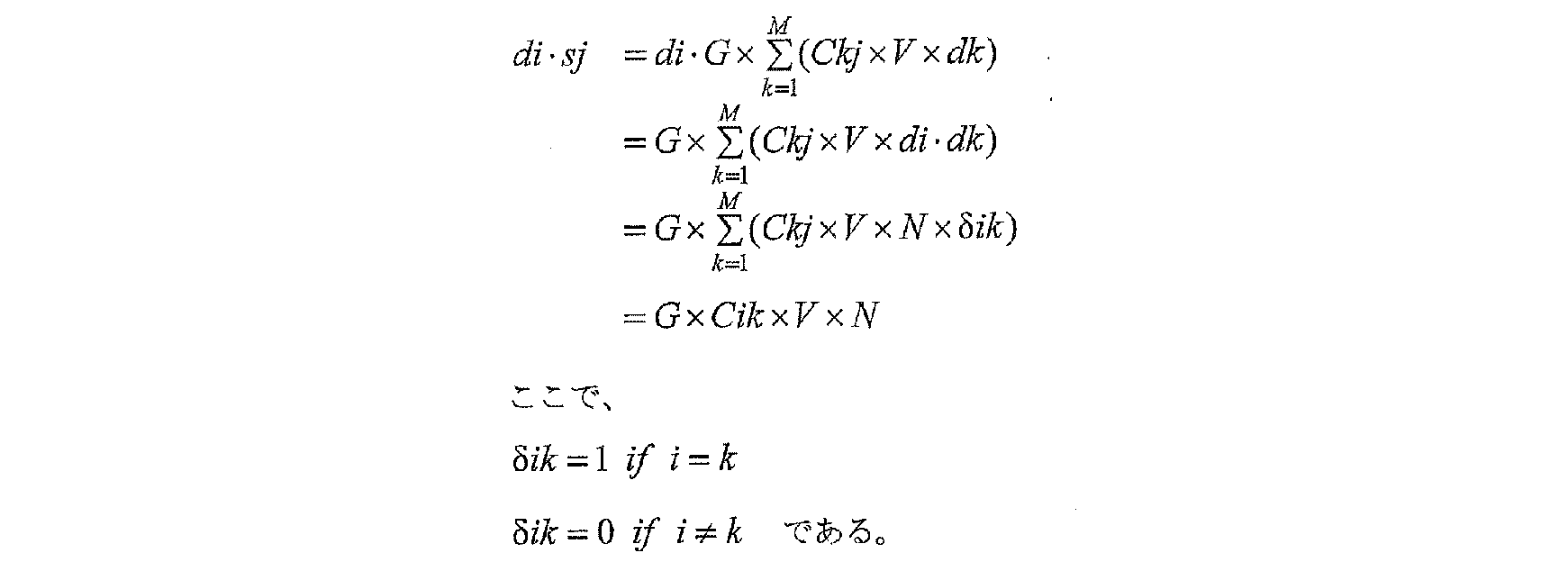
センスラインの読み出し方式としては、図1及び図2に示されるアナログ積分器6(積分容量Cintを用いたオペアンプによる電荷積分器)を使用すると、上記ゲインGは、(1/Cint)となる。
このように、集積回路3の駆動部4は、第1の静電容量列Cip(pは1以上(L-1)以下、i=1、…、M)、及び前記第2の静電容量列Ciq(p<q、qは2以上L以下、i=1、…、M)のそれぞれに対して、各要素が+1または-1によって構成される長さNの直交する符号系列di=(di1、di2、…、diN)(i=1、…、M)に基づいて、符号系列が前記+1の場合は+Vボルト、-1の場合は-Vボルトを印加するようにM本のドライブラインを並列に駆動する。そして、第1の静電容量列からの出力sFirst=(sp1、sp2、…、spN)、及び、第2の静電容量列からの出力sSecond=(sq1、sq2、…、sqN)を出力させる。
そして、上記第1の静電容量列からの出力sFirst=(sp1、sp2、…、spN)は、対応して設けられたアナログ積分器6によって積分され、第2の静電容量列からの出力sSecond=(sq1、sq2、…、sqN)は、対応して設けられたアナログ積分器6によって積分される。スイッチ7は、各センスラインSL1~SLLに対応するアナログ積分器6を順次切り換えて、各アナログ積分器6により積分された静電容量列からの出力をAD変換器8に供給する。
具体的には、まず、第1の静電容量列から出力sp1がアナログ積分器6に読み出されて積分されると同時に第2の静電容量列から出力sq1が他のアナログ積分器6に読み出されて積分される。そして、スイッチ7は、アナログ積分器6に接続し、読み出されて積分された出力sp1をADC8に供給する。次に、スイッチ7は、アナログ積分器6との接続を解除して他のアナログ積分器6に接続し、読み出されて積分された出力sq1をADC8に供給する。その後、第1の静電容量列から出力sp2がアナログ積分器6に読み出されて積分されると同時に第2の静電容量列から出力sq2が他のアナログ積分器6に読み出されて積分される。そして、スイッチ7は、アナログ積分器6に接続し、読み出されて積分された出力sp2をADC8に供給する。次に、スイッチ7は、アナログ積分器6との接続を解除して他のアナログ積分器6に接続し、読み出されて積分された出力sq2をADC8に供給する。このようにして、出力spN、出力sqNまでがアナログ積分器6及びスイッチ7により順番にADC8に供給される。また、ドライブラインの駆動に合わせて全センスラインのアナログ積分器6が並列に動作する。
AD変換器8は、アナログ積分器6により積分された静電容量列からの出力をAD変換して内積演算部9に供給する。
内積演算部9は、出力sFirstと符号系列diとの内積演算に基づいて、RAM10に格納されたデータを参照しながら、k1番目(1≦k1<M)のドライブラインに対応する第1の静電容量列の容量値を推定し、出力sSecondと符号系列diとの内積演算に基づいて、k2番目(k1<k2、1<k1≦M)のドライブラインに対応する第2の静電容量列の容量値を推定する。
アプリケーション処理部11は、内積演算部9により推定された静電容量の容量値に基づいて、ジェスチャー認識処理を実行し、ジェスチャーコマンドを生成する。
(符号系列の具体例)
図5は、センサパネルに入力される直交する符号系列の具体例を説明するための図である。長さNの直交する符号系列diの具体例としては、例えば、下記に示す符号系列を挙げることができる。
図5は、センサパネルに入力される直交する符号系列の具体例を説明するための図である。長さNの直交する符号系列diの具体例としては、例えば、下記に示す符号系列を挙げることができる。
代表的な直交する符号系列であるアダマール(Hadamard)行列は、図5に示されるシルベスター(sylvester)法によって生成される。基本的な構造として、2行×2列の基本単位を作る。この基本単位の右上、左上、及び左下のビットは同一であり、右下はこれらのビット反転となっている。
次に、前述した2×2の基本要素を、右上、左上、右下、及び左下にブロックとして4つ合成して、4行×4列のビット配列の符号を作る。ここで、2×2の基本単位の作成と同様に、右下のブロックはビット反転となる。同様な手順で、8行×8列、16行×16列のビット配列の符号を生成する。これらの行列は、前述した本発明の「直交する」の定義を満足する。
本実施の形態において、例えば、センサパネル2のドライブラインが16本で構成されていれば、図4に示す16行×16列のビット配列の符号を直交する符号系列として使用することができる。ここで、アダマール(Hadamard)行列とは、要素が1または-1のいずれかであり、かつ各行が互いに直交であるような正方行列をいう。すなわち、アダマール行列の任意の2つの行は、互いに垂直なベクトルを表す。
本実施の形態に係る直交する符号系列は、N次のアダマール行列から任意にM行取り出した行列を使用することができる(ここで、M≦Nである)。以下に述べるように、シルベスター法以外の方法によるアダマール行列も本発明に適用することができる。
図6は直交する符号系列の他の具体例を説明するための図であり、図7は直交する符号系列のさらに他の具体例を説明するための図である。シルベスター法によるN次のアダマール行列は、N=2のべき乗になるが、Nが4の倍数であれば、アダマール行列は存在するという予想が存在し、例えば、図6には、N=12のときのアダマール行列が示されており、図7には、N=20のときのアダマール行列が示されている。これらのシルベスター法以外の方法によるアダマール行列も、本実施の形態に係る直交する符号系列として使用することができる。
(内積演算の実際)
内積マトリックスC’ij=di・sjの計算は次の手順で行う。
(1)まず、推定部5のRAM10(図2)に格納された内積マトリックスをC’ij=0にリセットする。
(2)時刻tk(k=1、…、Nのいずれか)のタイミングでi番目(i=1、…、M)のドライブラインDLiを電圧V×dikで並列に駆動し、各静電容量に電荷Cij×V×dikを充電する。
(3)各センスラインj(j=1、…、L)を対応するアナログ積分器6に接続し、時刻tkで充電した静電容量からの出力電圧sjkを読み出し、各L本のセンスラインに対応して配置されたL個アナログ積分器6にそれぞれ読み出された時刻tkにおけるL個の出力電圧sjkを、スイッチ7により順番にAD変換器8に供給してAD変換し、AD変換器8によりAD変換された時刻tkにおける出力電圧sjkを内積演算部9に供給する。内積演算部9に供給された時刻tkにおける出力電圧sjkは、

となる。
(4)内積演算部9は、AD変換器8から出力されたL個の出力電圧sjkのそれぞれと、RAM10に格納された符号系列dikに応じて加減算を行い(符号系列dik=1のときは加算し、dik=-1のときは減算する)、その結果に基づいてC’ijの値を更新する。

(5)符号系列の長さに相当するN回の処理が回るまでは、時刻をインクリメント(tk+1)し、(1)に戻る。以上の処理が終わると、C’ijの値は、内積の計算結果となる。
内積マトリックスC’ij=di・sjの計算は次の手順で行う。
(1)まず、推定部5のRAM10(図2)に格納された内積マトリックスをC’ij=0にリセットする。
(2)時刻tk(k=1、…、Nのいずれか)のタイミングでi番目(i=1、…、M)のドライブラインDLiを電圧V×dikで並列に駆動し、各静電容量に電荷Cij×V×dikを充電する。
(3)各センスラインj(j=1、…、L)を対応するアナログ積分器6に接続し、時刻tkで充電した静電容量からの出力電圧sjkを読み出し、各L本のセンスラインに対応して配置されたL個アナログ積分器6にそれぞれ読み出された時刻tkにおけるL個の出力電圧sjkを、スイッチ7により順番にAD変換器8に供給してAD変換し、AD変換器8によりAD変換された時刻tkにおける出力電圧sjkを内積演算部9に供給する。内積演算部9に供給された時刻tkにおける出力電圧sjkは、
(4)内積演算部9は、AD変換器8から出力されたL個の出力電圧sjkのそれぞれと、RAM10に格納された符号系列dikに応じて加減算を行い(符号系列dik=1のときは加算し、dik=-1のときは減算する)、その結果に基づいてC’ijの値を更新する。
ここで、タッチセンサシステム1においては、駆動部4がセンサパネル2に配置され、推定部5がセンサパネル2とは別に設けられた基板30に配置される。そのため、駆動部4を推定部5とともに基板30に配置する場合と比べて、センサパネル2の狭額縁化を実現できる。
詳しく説明すると、センサパネル2においては、M本のドライブラインDL1~DLMとL本のセンスラインSL1~SLLとが交差する関係にある。そのため、駆動部4を推定部5とともに基板30に配置する場合には、M本のドライブラインDL1~DLMと駆動部4とを接続する配線及びL本のセンスラインSL1~SLLと推定部5とを接続する配線のうち何れかを、センサパネル2の外縁に沿って引き回す必要がある。一方、本実施形態では、駆動部4がセンサパネル2に配置されるので、駆動部4とM本のドライブラインDL1~DLMとを接続する配線をセンサパネル2の外縁に沿って引き回す必要がなくなる。その結果、本実施形態では、駆動部4を推定部5とともに基板30に配置する場合と比べて、センサパネル2の狭額縁化を実現できる。
また、駆動部4は、シフトレジスタ20と、XOR回路22A~22Cとを備える。そのため、駆動部4の回路構成が簡単になる。その結果、駆動部4をセンサパネル2に配置することが容易にできる。
(実施の形態の応用例)
例えば、シフトレジスタ20は2相クロックで動作してもよい。この場合、駆動部4の誤動作を抑えることができる。
例えば、シフトレジスタ20は2相クロックで動作してもよい。この場合、駆動部4の誤動作を抑えることができる。
以上、本発明の実施形態について、詳述してきたが、これらはあくまでも例示であって、本発明は、上述の実施形態によって、何等、限定されない。
Claims (3)
- M本のドライブラインと1本のセンスラインの間に形成される第1の静電容量列Ci1(i=1、…、M)、及び、上記M本のドライブラインと他の1本のセンスラインの間に形成される第2の静電容量列Ci2(i=1、…、M)とを備えるセンサパネルと、
前記センサパネルを制御する集積回路とを備えたタッチセンサシステムであって、
前記集積回路は、前記第1の静電容量列Ci1(i=1、…、M)、及び前記第2の静電容量列Ci2(i=1、…、M)のそれぞれに対して、各要素が+1または-1によって構成される長さNの直交する符号系列di=(di1、di2、…、diN)(i=1、…、M、及びM<N)に基づいて、前記M本のドライブラインを並列に駆動して、前記第1の静電容量列からの出力sFirst=(s11、s12、…、s1N)、及び、前記第2の静電容量列からの出力sSecond=(s21、s22、…、s2N)をアナログ積分器に出力する駆動部と、
前記出力sFirstと前記符号系列diとの内積演算に基づいて、k1番目のドライブラインに対応する前記第1の静電容量列の容量値を推定し、前記出力sSecondと前記符号系列diとの内積演算に基づいて、k2番目のドライブラインに対応する前記第2の静電容量列の容量値を推定する推定部とを有しており、
前記駆動部が前記センサパネルに配置され、前記推定部が前記センサパネルの他に別途設けられた基板に配置される、タッチセンサシステム。 - 請求項1に記載のタッチセンサシステムであって、
前記駆動部は、
複数のフリップフロップをカスケード接続したシフトレジスタと、
前記シフトレジスタに設けられた中間タップに接続されるXOR回路とを備え、
前記複数のフリップフロップのそれぞれが有する出力は、前記M本のドライブラインにおいて互いに異なるドライブラインに接続される、タッチセンサシステム。 - 請求項2に記載のタッチセンサシステムであって、
前記シフトレジスタが2相クロックで動作する、タッチセンサシステム。
Applications Claiming Priority (2)
| Application Number | Priority Date | Filing Date | Title |
|---|---|---|---|
| JP2012-280598 | 2012-12-25 | ||
| JP2012280598 | 2012-12-25 |
Publications (1)
| Publication Number | Publication Date |
|---|---|
| WO2014103844A1 true WO2014103844A1 (ja) | 2014-07-03 |
Family
ID=51020931
Family Applications (1)
| Application Number | Title | Priority Date | Filing Date |
|---|---|---|---|
| PCT/JP2013/083961 Ceased WO2014103844A1 (ja) | 2012-12-25 | 2013-12-18 | タッチセンサシステム |
Country Status (1)
| Country | Link |
|---|---|
| WO (1) | WO2014103844A1 (ja) |
Citations (4)
| Publication number | Priority date | Publication date | Assignee | Title |
|---|---|---|---|---|
| JP2005303499A (ja) * | 2004-04-08 | 2005-10-27 | Nippon Telegr & Teleph Corp <Ntt> | 拡散符号生成回路および同期回路 |
| JP2011233018A (ja) * | 2010-04-28 | 2011-11-17 | Sony Corp | タッチ検出機能付き表示装置、駆動方法、および電子機器 |
| JP4927216B1 (ja) * | 2010-11-12 | 2012-05-09 | シャープ株式会社 | 線形素子列値推定方法、静電容量検出方法、集積回路、タッチセンサシステム、及び電子機器 |
| WO2012147634A1 (ja) * | 2011-04-28 | 2012-11-01 | シャープ株式会社 | 入力装置、接触位置検出方法、および入力装置を備える表示装置 |
-
2013
- 2013-12-18 WO PCT/JP2013/083961 patent/WO2014103844A1/ja not_active Ceased
Patent Citations (4)
| Publication number | Priority date | Publication date | Assignee | Title |
|---|---|---|---|---|
| JP2005303499A (ja) * | 2004-04-08 | 2005-10-27 | Nippon Telegr & Teleph Corp <Ntt> | 拡散符号生成回路および同期回路 |
| JP2011233018A (ja) * | 2010-04-28 | 2011-11-17 | Sony Corp | タッチ検出機能付き表示装置、駆動方法、および電子機器 |
| JP4927216B1 (ja) * | 2010-11-12 | 2012-05-09 | シャープ株式会社 | 線形素子列値推定方法、静電容量検出方法、集積回路、タッチセンサシステム、及び電子機器 |
| WO2012147634A1 (ja) * | 2011-04-28 | 2012-11-01 | シャープ株式会社 | 入力装置、接触位置検出方法、および入力装置を備える表示装置 |
Similar Documents
| Publication | Publication Date | Title |
|---|---|---|
| JP4927216B1 (ja) | 線形素子列値推定方法、静電容量検出方法、集積回路、タッチセンサシステム、及び電子機器 | |
| US8942937B2 (en) | Linear device value estimating method, capacitance detection method, integrated circuit, touch sensor system, and electronic device | |
| US11042715B2 (en) | Electronic system for performing a multiplication of a matrix and vector | |
| CN109979396A (zh) | 栅极驱动电路、触控显示装置及驱动方法 | |
| JP4779853B2 (ja) | ディジタル−アナログ変換器および映像表示装置 | |
| CN105047120B (zh) | 一种栅极驱动电路及其驱动方法、显示装置 | |
| EP3086309B1 (en) | Ramp signal generation circuit and signal generator, array substrate and display device | |
| CN108027686A (zh) | 电容检测方法、位置检测方法、触摸面板控制器及电子设备 | |
| US9755624B2 (en) | Ramp signal generating circuit and signal generator, array substrate and display apparatus | |
| WO2014002907A1 (ja) | タッチパネルコントローラ、集積回路、タッチパネル装置、及び電子機器 | |
| WO2020255599A1 (ja) | 演算装置及び積和演算システム | |
| TWI617966B (zh) | 觸控面板 | |
| JP5865791B2 (ja) | A/d変換器、半導体装置 | |
| US10534488B2 (en) | Capacitance detection method, position detection method, touch panel controller, and electronic device | |
| WO2014103844A1 (ja) | タッチセンサシステム | |
| US20180329548A1 (en) | Display module, touch panel controller, and electronic device | |
| JP3522492B2 (ja) | 複素係数乗算器および複素係数フィルタ | |
| JP2007235379A (ja) | デジタル/アナログ変換回路 | |
| JP5670586B2 (ja) | 線形素子値推定方法、静電容量検出方法、集積回路、タッチセンサシステム、電子機器 | |
| WO2014038519A1 (ja) | タッチパネルコントローラ、及びこれを含む集積回路、タッチパネル装置、電子機器 | |
| EP4075342A1 (en) | Convolution engine for in-memory computing | |
| JPH09259206A (ja) | 離散コサイン変換回路 | |
| Vykhovanets | Additive algebra for Digital Signal Processing | |
| WO2014129091A1 (ja) | タッチパネルコントローラ、集積回路、タッチパネル装置、及び、電子機器 | |
| WO2014007223A1 (ja) | タッチパネルコントローラ、及びこれを用いた集積回路、タッチパネル装置、電子機器 |
Legal Events
| Date | Code | Title | Description |
|---|---|---|---|
| 121 | Ep: the epo has been informed by wipo that ep was designated in this application |
Ref document number: 13869507 Country of ref document: EP Kind code of ref document: A1 |
|
| NENP | Non-entry into the national phase |
Ref country code: DE |
|
| 122 | Ep: pct application non-entry in european phase |
Ref document number: 13869507 Country of ref document: EP Kind code of ref document: A1 |
|
| NENP | Non-entry into the national phase |
Ref country code: JP |