WO2014103584A1 - 半導体膜、半導体膜の製造方法、太陽電池、発光ダイオード、薄膜トランジスタ、および、電子デバイス - Google Patents
半導体膜、半導体膜の製造方法、太陽電池、発光ダイオード、薄膜トランジスタ、および、電子デバイス Download PDFInfo
- Publication number
- WO2014103584A1 WO2014103584A1 PCT/JP2013/081498 JP2013081498W WO2014103584A1 WO 2014103584 A1 WO2014103584 A1 WO 2014103584A1 JP 2013081498 W JP2013081498 W JP 2013081498W WO 2014103584 A1 WO2014103584 A1 WO 2014103584A1
- Authority
- WO
- WIPO (PCT)
- Prior art keywords
- semiconductor
- ligand
- semiconductor film
- quantum dot
- film according
- Prior art date
- Legal status (The legal status is an assumption and is not a legal conclusion. Google has not performed a legal analysis and makes no representation as to the accuracy of the status listed.)
- Ceased
Links
Images


Classifications
-
- H—ELECTRICITY
- H10—SEMICONDUCTOR DEVICES; ELECTRIC SOLID-STATE DEVICES NOT OTHERWISE PROVIDED FOR
- H10F—INORGANIC SEMICONDUCTOR DEVICES SENSITIVE TO INFRARED RADIATION, LIGHT, ELECTROMAGNETIC RADIATION OF SHORTER WAVELENGTH OR CORPUSCULAR RADIATION
- H10F77/00—Constructional details of devices covered by this subclass
- H10F77/10—Semiconductor bodies
- H10F77/14—Shape of semiconductor bodies; Shapes, relative sizes or dispositions of semiconductor regions within semiconductor bodies
- H10F77/143—Shape of semiconductor bodies; Shapes, relative sizes or dispositions of semiconductor regions within semiconductor bodies comprising quantum structures
- H10F77/1433—Quantum dots
-
- C—CHEMISTRY; METALLURGY
- C09—DYES; PAINTS; POLISHES; NATURAL RESINS; ADHESIVES; COMPOSITIONS NOT OTHERWISE PROVIDED FOR; APPLICATIONS OF MATERIALS NOT OTHERWISE PROVIDED FOR
- C09K—MATERIALS FOR MISCELLANEOUS APPLICATIONS, NOT PROVIDED FOR ELSEWHERE
- C09K11/00—Luminescent, e.g. electroluminescent, chemiluminescent materials
- C09K11/02—Use of particular materials as binders, particle coatings or suspension media therefor
- C09K11/025—Use of particular materials as binders, particle coatings or suspension media therefor non-luminescent particle coatings or suspension media
-
- C—CHEMISTRY; METALLURGY
- C09—DYES; PAINTS; POLISHES; NATURAL RESINS; ADHESIVES; COMPOSITIONS NOT OTHERWISE PROVIDED FOR; APPLICATIONS OF MATERIALS NOT OTHERWISE PROVIDED FOR
- C09K—MATERIALS FOR MISCELLANEOUS APPLICATIONS, NOT PROVIDED FOR ELSEWHERE
- C09K11/00—Luminescent, e.g. electroluminescent, chemiluminescent materials
- C09K11/08—Luminescent, e.g. electroluminescent, chemiluminescent materials containing inorganic luminescent materials
- C09K11/66—Luminescent, e.g. electroluminescent, chemiluminescent materials containing inorganic luminescent materials containing germanium, tin or lead
- C09K11/661—Chalcogenides
-
- H—ELECTRICITY
- H01—ELECTRIC ELEMENTS
- H01L—SEMICONDUCTOR DEVICES NOT COVERED BY CLASS H10
- H01L21/00—Processes or apparatus adapted for the manufacture or treatment of semiconductor or solid state devices or of parts thereof
- H01L21/02—Manufacture or treatment of semiconductor devices or of parts thereof
- H01L21/02104—Forming layers
- H01L21/02365—Forming inorganic semiconducting materials on a substrate
- H01L21/02518—Deposited layers
- H01L21/02521—Materials
- H01L21/02568—Chalcogenide semiconducting materials not being oxides, e.g. ternary compounds
-
- H—ELECTRICITY
- H01—ELECTRIC ELEMENTS
- H01L—SEMICONDUCTOR DEVICES NOT COVERED BY CLASS H10
- H01L21/00—Processes or apparatus adapted for the manufacture or treatment of semiconductor or solid state devices or of parts thereof
- H01L21/02—Manufacture or treatment of semiconductor devices or of parts thereof
- H01L21/02104—Forming layers
- H01L21/02365—Forming inorganic semiconducting materials on a substrate
- H01L21/02518—Deposited layers
- H01L21/02587—Structure
- H01L21/0259—Microstructure
- H01L21/02601—Nanoparticles
-
- H—ELECTRICITY
- H01—ELECTRIC ELEMENTS
- H01L—SEMICONDUCTOR DEVICES NOT COVERED BY CLASS H10
- H01L21/00—Processes or apparatus adapted for the manufacture or treatment of semiconductor or solid state devices or of parts thereof
- H01L21/02—Manufacture or treatment of semiconductor devices or of parts thereof
- H01L21/02104—Forming layers
- H01L21/02365—Forming inorganic semiconducting materials on a substrate
- H01L21/02612—Formation types
- H01L21/02617—Deposition types
- H01L21/02623—Liquid deposition
-
- H—ELECTRICITY
- H10—SEMICONDUCTOR DEVICES; ELECTRIC SOLID-STATE DEVICES NOT OTHERWISE PROVIDED FOR
- H10D—INORGANIC ELECTRIC SEMICONDUCTOR DEVICES
- H10D30/00—Field-effect transistors [FET]
- H10D30/60—Insulated-gate field-effect transistors [IGFET]
- H10D30/67—Thin-film transistors [TFT]
- H10D30/6757—Thin-film transistors [TFT] characterised by the structure of the channel, e.g. transverse or longitudinal shape or doping profile
-
- H—ELECTRICITY
- H10—SEMICONDUCTOR DEVICES; ELECTRIC SOLID-STATE DEVICES NOT OTHERWISE PROVIDED FOR
- H10D—INORGANIC ELECTRIC SEMICONDUCTOR DEVICES
- H10D62/00—Semiconductor bodies, or regions thereof, of devices having potential barriers
- H10D62/80—Semiconductor bodies, or regions thereof, of devices having potential barriers characterised by the materials
- H10D62/81—Semiconductor bodies, or regions thereof, of devices having potential barriers characterised by the materials of structures exhibiting quantum-confinement effects, e.g. single quantum wells; of structures having periodic or quasi-periodic potential variation
- H10D62/812—Single quantum well structures
- H10D62/814—Quantum box structures
-
- H—ELECTRICITY
- H10—SEMICONDUCTOR DEVICES; ELECTRIC SOLID-STATE DEVICES NOT OTHERWISE PROVIDED FOR
- H10D—INORGANIC ELECTRIC SEMICONDUCTOR DEVICES
- H10D99/00—Subject matter not provided for in other groups of this subclass
-
- H—ELECTRICITY
- H10—SEMICONDUCTOR DEVICES; ELECTRIC SOLID-STATE DEVICES NOT OTHERWISE PROVIDED FOR
- H10F—INORGANIC SEMICONDUCTOR DEVICES SENSITIVE TO INFRARED RADIATION, LIGHT, ELECTROMAGNETIC RADIATION OF SHORTER WAVELENGTH OR CORPUSCULAR RADIATION
- H10F10/00—Individual photovoltaic cells, e.g. solar cells
- H10F10/10—Individual photovoltaic cells, e.g. solar cells having potential barriers
- H10F10/16—Photovoltaic cells having only PN heterojunction potential barriers
- H10F10/164—Photovoltaic cells having only PN heterojunction potential barriers comprising heterojunctions with Group IV materials, e.g. ITO/Si or GaAs/SiGe photovoltaic cells
-
- H—ELECTRICITY
- H10—SEMICONDUCTOR DEVICES; ELECTRIC SOLID-STATE DEVICES NOT OTHERWISE PROVIDED FOR
- H10F—INORGANIC SEMICONDUCTOR DEVICES SENSITIVE TO INFRARED RADIATION, LIGHT, ELECTROMAGNETIC RADIATION OF SHORTER WAVELENGTH OR CORPUSCULAR RADIATION
- H10F71/00—Manufacture or treatment of devices covered by this subclass
-
- H—ELECTRICITY
- H10—SEMICONDUCTOR DEVICES; ELECTRIC SOLID-STATE DEVICES NOT OTHERWISE PROVIDED FOR
- H10F—INORGANIC SEMICONDUCTOR DEVICES SENSITIVE TO INFRARED RADIATION, LIGHT, ELECTROMAGNETIC RADIATION OF SHORTER WAVELENGTH OR CORPUSCULAR RADIATION
- H10F77/00—Constructional details of devices covered by this subclass
- H10F77/10—Semiconductor bodies
- H10F77/12—Active materials
- H10F77/127—Active materials comprising only Group IV-VI or only Group II-IV-VI chalcogenide materials, e.g. PbSnTe
-
- H—ELECTRICITY
- H10—SEMICONDUCTOR DEVICES; ELECTRIC SOLID-STATE DEVICES NOT OTHERWISE PROVIDED FOR
- H10F—INORGANIC SEMICONDUCTOR DEVICES SENSITIVE TO INFRARED RADIATION, LIGHT, ELECTROMAGNETIC RADIATION OF SHORTER WAVELENGTH OR CORPUSCULAR RADIATION
- H10F77/00—Constructional details of devices covered by this subclass
- H10F77/10—Semiconductor bodies
- H10F77/16—Material structures, e.g. crystalline structures, film structures or crystal plane orientations
- H10F77/162—Non-monocrystalline materials, e.g. semiconductor particles embedded in insulating materials
- H10F77/1625—Semiconductor nanoparticles embedded in semiconductor matrix
-
- H—ELECTRICITY
- H10—SEMICONDUCTOR DEVICES; ELECTRIC SOLID-STATE DEVICES NOT OTHERWISE PROVIDED FOR
- H10H—INORGANIC LIGHT-EMITTING SEMICONDUCTOR DEVICES HAVING POTENTIAL BARRIERS
- H10H20/00—Individual inorganic light-emitting semiconductor devices having potential barriers, e.g. light-emitting diodes [LED]
- H10H20/01—Manufacture or treatment
-
- H—ELECTRICITY
- H10—SEMICONDUCTOR DEVICES; ELECTRIC SOLID-STATE DEVICES NOT OTHERWISE PROVIDED FOR
- H10H—INORGANIC LIGHT-EMITTING SEMICONDUCTOR DEVICES HAVING POTENTIAL BARRIERS
- H10H20/00—Individual inorganic light-emitting semiconductor devices having potential barriers, e.g. light-emitting diodes [LED]
- H10H20/80—Constructional details
- H10H20/81—Bodies
- H10H20/811—Bodies having quantum effect structures or superlattices, e.g. tunnel junctions
- H10H20/812—Bodies having quantum effect structures or superlattices, e.g. tunnel junctions within the light-emitting regions, e.g. having quantum confinement structures
-
- H—ELECTRICITY
- H10—SEMICONDUCTOR DEVICES; ELECTRIC SOLID-STATE DEVICES NOT OTHERWISE PROVIDED FOR
- H10H—INORGANIC LIGHT-EMITTING SEMICONDUCTOR DEVICES HAVING POTENTIAL BARRIERS
- H10H20/00—Individual inorganic light-emitting semiconductor devices having potential barriers, e.g. light-emitting diodes [LED]
- H10H20/80—Constructional details
- H10H20/81—Bodies
- H10H20/822—Materials of the light-emitting regions
-
- Y—GENERAL TAGGING OF NEW TECHNOLOGICAL DEVELOPMENTS; GENERAL TAGGING OF CROSS-SECTIONAL TECHNOLOGIES SPANNING OVER SEVERAL SECTIONS OF THE IPC; TECHNICAL SUBJECTS COVERED BY FORMER USPC CROSS-REFERENCE ART COLLECTIONS [XRACs] AND DIGESTS
- Y02—TECHNOLOGIES OR APPLICATIONS FOR MITIGATION OR ADAPTATION AGAINST CLIMATE CHANGE
- Y02E—REDUCTION OF GREENHOUSE GAS [GHG] EMISSIONS, RELATED TO ENERGY GENERATION, TRANSMISSION OR DISTRIBUTION
- Y02E10/00—Energy generation through renewable energy sources
- Y02E10/50—Photovoltaic [PV] energy
- Y02E10/549—Organic PV cells
-
- Y—GENERAL TAGGING OF NEW TECHNOLOGICAL DEVELOPMENTS; GENERAL TAGGING OF CROSS-SECTIONAL TECHNOLOGIES SPANNING OVER SEVERAL SECTIONS OF THE IPC; TECHNICAL SUBJECTS COVERED BY FORMER USPC CROSS-REFERENCE ART COLLECTIONS [XRACs] AND DIGESTS
- Y02—TECHNOLOGIES OR APPLICATIONS FOR MITIGATION OR ADAPTATION AGAINST CLIMATE CHANGE
- Y02P—CLIMATE CHANGE MITIGATION TECHNOLOGIES IN THE PRODUCTION OR PROCESSING OF GOODS
- Y02P70/00—Climate change mitigation technologies in the production process for final industrial or consumer products
- Y02P70/50—Manufacturing or production processes characterised by the final manufactured product
Definitions
- the present invention relates to a semiconductor film, a semiconductor film manufacturing method, a solar cell, a light emitting diode, a thin film transistor, and an electronic device.
- third-generation solar cells In recent years, research on high-efficiency solar cells called third-generation solar cells has been actively conducted. Among them, solar cells using colloidal quantum dots have been attracting attention because, for example, it has been reported that quantum efficiency can be increased by the effect of multi-exciton generation. However, in a solar cell using colloidal quantum dots (also referred to as a quantum dot solar cell), the conversion efficiency is about 7% at the maximum, and further improvement in conversion efficiency is required.
- Patent Document 1 Patent No. 4425470
- Patent Document 2 Japanese Patent Publication No. 2011-513508
- Non-Patent Document 1 S. Geyer et al., “Charge transport in mixed CdSe and CdTe colloidal nanofilms”, Physical Review B and Non-Patent Documents 2010. 2 (written by JM Luther et al., “Structural, Optical, and Electrical Properties of Self-Assembled Films of PbSe Nanocrystal.
- Non-Patent Document 2 by replacing oleic acid (molecular chain length of about 2 nm to 3 nm) around the PbSe quantum dots with ethanedithiol (molecular chain length of 1 nm or less), the quantum dots are brought close to each other, and the electrical conductivity is improved. It has been reported to improve.
- the semiconductor film described in Patent Document 1 has a large ligand and insufficient proximity of the semiconductor quantum dots, so that the photoelectric conversion characteristics are not excellent.
- the semiconductor film described in Patent Document 1 has a large ligand and insufficient proximity of the semiconductor quantum dots, so that the photoelectric conversion characteristics are not excellent.
- butylamine used in Non-Patent Document 1 or ethanedithiol used in Non-Patent Document 2 is used as a ligand, for example, according to Non-Patent Document 1, several hundreds at the maximum. Only a photocurrent value of about nA can be obtained. Further, when ethanedithiol was used as a ligand, the semiconductor film was easily peeled off.
- An object of the present invention is to provide a semiconductor film in which a high photocurrent value is obtained and film peeling is suppressed, and a method for manufacturing the semiconductor film, and an object thereof is to solve the problem. It is another object of the present invention to provide a solar cell, a light emitting diode, a thin film transistor, and an electronic device in which a high photocurrent value is obtained and film peeling is suppressed, and to solve the problem.
- X 1 represents NH, S, or O
- X 2 and X 3 each independently represent NH 2 , SH, or OH
- n and m each independently represent an integer of 1 or more and 3 or less.
- the ⁇ 2> ligand is the semiconductor film according to ⁇ 1>, wherein at least one of (CH 2 ) m and (CH 2 ) n further has a substituent having 10 or less atoms.
- the substituent is the semiconductor film according to ⁇ 2>, wherein the number of atoms is 7 or less.
- X 1 is the semiconductor film according to any one of ⁇ 1> to ⁇ 4>, which is NH.
- At least the ligand is selected from the group consisting of diethanolamine, diethylenetriamine, 2- (2-aminoethylamino) ethanol, diethanolamine derivatives, diethylenetriamine derivatives, and 2- (2-aminoethylamino) ethanol derivatives
- the ligand is the semiconductor film according to any one of ⁇ 1> to ⁇ 6>, which is tridentate with respect to the metal atom in the semiconductor quantum dot.
- ⁇ 8> is a semiconductor film according to any one of ⁇ 1> to ⁇ 7> complex stability constant Logbeta 1 is 5 or more between the ligand and the semiconductor quantum dots of the metal atoms.
- the semiconductor quantum dot is the semiconductor film according to any one of ⁇ 1> to ⁇ 8>, including at least one selected from the group consisting of PbS, PbSe, InN, InAs, InSb, and InP. is there.
- the semiconductor quantum dot is the semiconductor film according to any one of ⁇ 1> to ⁇ 9>, which has an average particle diameter of 2 nm to 15 nm.
- the semiconductor quantum dot is the semiconductor film according to ⁇ 9> or ⁇ 10> containing PbS.
- a semiconductor quantum dot dispersion liquid containing a semiconductor quantum dot containing a metal atom, a first ligand coordinated to the semiconductor quantum dot, and a first solvent is provided on the substrate.
- X 1 represents NH, S, or O
- X 2 and X 3 each independently represent NH 2 , SH, or OH
- n and m each independently represent an integer of 1 or more and 3 or less.
- the substituent is the method for producing a semiconductor film according to ⁇ 13>, wherein the number of atoms is 7 or less.
- ⁇ 16> The method for producing a semiconductor film according to any one of ⁇ 12> to ⁇ 15>, wherein the semiconductor quantum dot assembly forming step and the ligand exchange step are each performed twice or more.
- X 1 is a method of manufacturing a semiconductor film according to any one of a NH ⁇ 12> ⁇ ⁇ 16> .
- the second ligand is selected from the group consisting of diethanolamine, diethylenetriamine, 2- (2-aminoethylamino) ethanol, diethanolamine derivatives, diethylenetriamine derivatives, and 2- (2-aminoethylamino) ethanol derivatives.
- ⁇ 22> The semiconductor quantum dot manufacturing method according to any one of ⁇ 12> to ⁇ 21>, wherein the average particle diameter is 2 nm to 15 nm.
- the semiconductor quantum dot is the method for producing a semiconductor film according to ⁇ 21> or ⁇ 22>, which includes PbS.
- a solar cell comprising the semiconductor film according to any one of ⁇ 1> to ⁇ 11>.
- a light emitting diode comprising the semiconductor film according to any one of ⁇ 1> to ⁇ 11>.
- An electronic device comprising the semiconductor film according to any one of ⁇ 1> to ⁇ 11>.
- the semiconductor film which can obtain a high photocurrent value and suppresses film peeling and its manufacturing method are provided.
- a solar cell a light emitting diode, a thin film transistor, and an electronic device in which a high photocurrent value is obtained and film peeling is suppressed.
- the semiconductor film of this invention has the aggregate
- the “ligand represented by the general formula (A)” is also referred to as “specific ligand”.
- X 1 represents NH, S, or O
- X 2 and X 3 each independently represent NH 2 , SH, or OH
- n and m each independently represent an integer of 1 or more and 3 or less.
- a semiconductor quantum dot is a semiconductor particle including a metal atom, and is a nano-sized particle having a particle size of several nanometers to several tens of nanometers.
- the specific ligand represented by the general formula (A) is bonded to the semiconductor quantum dots by coordination bonds, it is considered that the interval between the semiconductor quantum dots is shortened. . This is because the specific ligand has the molecular structure as described above, so that NH, S or O represented by X 1 at the center of the molecule, and SH, NH represented by X 2 or X 3 at the molecular end.
- the formation of tridentate or more multidentate coordination between the specific ligand and the metal atom strongly compensates for dangling bonds on the surface of the semiconductor quantum dots, and the spacing between the semiconductor quantum dots as described above. Are likely to be close to each other, and as a result, high electrical conductivity is likely to be easily obtained. Therefore, it is considered that the semiconductor film of the present invention can obtain a high photocurrent value and suppress film peeling.
- the semiconductor film of the present invention has a complex stability constant log ⁇ between a specific ligand and a metal atom of the semiconductor quantum dots. 1 is preferably 5 or more.
- the complex stability constant is a constant determined by the relationship between the ligand and the metal atom to be coordinated, and is represented by the following formula (b).
- [ML] represents the molar concentration of the complex in which the metal atom and the ligand are bonded
- [M] represents the molar concentration of the metal atom that can contribute to the coordination bond
- [L ] Represents the molar concentration of the ligand.
- a plurality of ligands may coordinate to one metal atom.
- the ligand is represented by the formula (b) in the case where one ligand molecule coordinates to one metal atom.
- the complex stability constant log ⁇ defined as an index of the strength of the coordination bond.
- a complex stability constant log ⁇ 1 between the specific ligand and the metal atom of the semiconductor quantum dot is 5 or more, whereby a complex is easily formed.
- Complex stability constant Logbeta 1 in combination with the semiconductor quantum dot and the ligand, the higher is desirable. If the ligand is multidentate like a chelate, the bond strength can be further increased.
- Logbeta 1 specific ligand will vary by semiconductor quantum dot material constituting the semiconductor quantum dot is changed, the specific ligand, the molecular chain length is short and coordinated Since it is easy, it is applicable to various semiconductor quantum dot materials.
- log ⁇ 1 is more preferably 8 or more, and further preferably 10 or more.
- the semiconductor film of the present invention contains at least one specific ligand.
- X 1 represents NH, S, or O
- X 2 and X 3 each independently represent NH 2 , SH, or OH.
- n and m each independently represent an integer of 1 or more and 3 or less.
- (CH 2 ) m and (CH 2 ) n may each independently have a substituent having 1 to 10 atoms (preferably 7 or less). Only one of (CH 2 ) m and (CH 2 ) n may have a substituent, or both may have a substituent.
- (CH 2 ) m or (CH 2 ) n has a substituent means a state in which a substituent is bonded to a carbon atom instead of a hydrogen atom bonded to a carbon atom.
- Examples of the “substituent having 1 to 10 atoms” that (CH 2 ) m and (CH 2 ) n may have independently include an alkyl group having 1 to 3 carbon atoms [methyl group, ethyl group, propyl group, And isopropyl group], alkenyl group having 2 to 3 carbon atoms [ethenyl group and propenyl group], alkynyl group having 2 to 4 carbon atoms [ethynyl group, propynyl group, etc.], cyclopropyl group, alkoxy group having 1 to 2 carbon atoms [Methoxy group and ethoxy group], acyl group having 2 to 3 carbon atoms [acetyl group and propionyl group], alkoxycarbonyl group having 2 to 3 carbon atoms [methoxycarbonyl group and ethoxycarbonyl group], acyloxy group having 2 carbon atoms [Acetyloxy group], acylamino group having 2 carbon atom
- the substituent may further have a substituent as long as the total number of atoms as the substituent is 10 or less. Since the number of atoms of the substituent is 10 or less, steric hindrance due to the ligand can be suppressed and the semiconductor quantum dots can be brought close to each other, so that the electrical conductivity of the semiconductor film can be increased. From the viewpoint of shortening the distance between the semiconductor quantum dots, the substituent preferably has 7 or less atoms. Further, (CH 2 ) m and (CH 2 ) n are more preferably unsubstituted.
- X 1 in the general formula (A) is preferably NH, and X 2 and X 3 are preferably NH 2 .
- X 2 and X 3 in the general formula (A) is OH (hydroxy group).
- Specific examples of the compound represented by the general formula (A) include diethanolamine, diethylenetriamine, 2- (2-aminoethylamino) ethanol, N- (3-aminopropyl) -1,3-propanediamine, and diethanolamine.
- Examples include methylenetriamine, 1,1-oxybismethylamine, 1,1-thiobismethylamine, 2-[(2-aminoethyl) amino] ethanethiol, and bis (2-mercaptoethyl) amine.
- the specific ligand may be a derivative of a compound represented by the general formula (A) such as a diethanolamine derivative, a diethylenetriamine derivative, and a 2- (2-aminoethylamino) ethanol derivative.
- A a compound represented by the general formula (A) such as a diethanolamine derivative, a diethylenetriamine derivative, and a 2- (2-aminoethylamino) ethanol derivative.
- a particularly high photocurrent value can be obtained as compared with the case where ethanedithiol is used as the ligand.
- diethanolamine, diethylenetriamine, 2- (2-aminoethylamino) ethanol, 2-[(2-aminoethyl) amino] ethanethiol, or bis (2-mercaptoethyl) amine is used as a ligand.
- the effect of increasing the photocurrent value is great. This is probably due to the following two reasons.
- the dangling bond of the metal atom in the semiconductor quantum dot, X 1 represented by the general formula (A), and X 2 (or X 3 ) form a five-membered ring chelate, thereby achieving high complex stability. It becomes easy to obtain a constant (log ⁇ ).
- the specific ligand is chelate-coordinated to the metal atom in the semiconductor quantum dot, so that steric hindrance between the semiconductor quantum dots is suppressed, and as a result, high electrical conductivity is easily obtained.
- the semiconductor film of the present invention may contain two or more kinds of specific ligands.
- the semiconductor film of the present invention has an aggregate of semiconductor quantum dots. Moreover, the semiconductor quantum dot has at least one kind of metal atom.
- the aggregate of semiconductor quantum dots refers to a form in which a large number (for example, 100 or more per 1 ⁇ m 2 square) of semiconductor quantum dots are arranged close to each other.
- the “semiconductor” in the present invention means a substance having a specific resistance value of 10 ⁇ 2 ⁇ cm or more and 10 8 ⁇ cm or less.
- the semiconductor quantum dot is a semiconductor particle having a metal atom.
- the metal atom includes a semimetal atom represented by Si atom.
- the semiconductor quantum dot material constituting the semiconductor quantum dot include a general semiconductor crystal [a) a group IV semiconductor, b) a compound semiconductor of group IV-IV, group III-V, or group II-VI, c) II Compound semiconductor composed of a combination of three or more of group III, group IV, group IV, group V, and group VI elements (particles having a size of 0.5 nm to less than 100 nm).
- semiconductor materials having a relatively narrow band gap such as PbS, PbSe, InN, InAs, Ge, InAs, InGaAs, CuInS, CuInSe, CuInGaSe, InSb, Si, and InP.
- the semiconductor quantum dot should just contain at least 1 type of semiconductor quantum dot material.
- the semiconductor quantum dot material has a bulk band gap of 1.5 eV or less.
- the semiconductor film of the present invention is used, for example, in a photoelectric conversion layer of a solar cell.
- the semiconductor quantum dot may have a core-shell structure in which the semiconductor quantum dot material is a core and the semiconductor quantum dot material is covered with a coating compound.
- the coating compound include ZnS, ZnSe, ZnTe, ZnCdS, and the like.
- the semiconductor quantum dot material is preferably PbS or PbSe because of the ease of synthesis of the semiconductor quantum dots. It is also desirable to use InN from the viewpoint that the environmental load is small.
- the semiconductor quantum dot may have a narrower band gap in view of enhancement of photoelectric conversion efficiency due to a multi-exciton generation effect called a multi-exciton generation effect.
- a multi-exciton generation effect preferable.
- the semiconductor quantum dot material is preferably PbS, PbSe, or InSb.
- the average particle diameter of the semiconductor quantum dots is desirably 2 nm to 15 nm.
- the average particle diameter of a semiconductor quantum dot means the average particle diameter of ten semiconductor quantum dots.
- a transmission electron microscope may be used to measure the particle size of the semiconductor quantum dots.
- the “average particle size” of the semiconductor quantum dots in the present specification refers to the number average particle size unless otherwise specified. That is, the number average particle diameter of the semiconductor quantum dots is desirably 2 nm to 15 nm.
- semiconductor quantum dots include particles of various sizes from several nm to several tens of nm.
- the semiconductor quantum dot when the average particle diameter of the quantum dot is reduced to a size equal to or less than the Bohr radius of the underlying electron, a phenomenon occurs in which the band gap of the semiconductor quantum dot changes due to the quantum size effect.
- II-VI semiconductors have a relatively large Bohr radius, and PbS is said to have a Bohr radius of about 18 nm.
- InP which is a group III-V semiconductor, is said to have a Bohr radius of about 10 nm to 14 nm. Therefore, for example, if the average particle size of the semiconductor quantum dots is 15 nm or less, the band gap can be controlled by the quantum size effect.
- the semiconductor film of the present invention when the semiconductor film of the present invention is applied to a solar cell, it is important to adjust the band gap to an optimum value by the quantum size effect regardless of the semiconductor quantum dot material.
- the band gap increases as the average particle size of the semiconductor quantum dots decreases, a larger change in the band gap can be expected if the average particle size of the semiconductor quantum dots is 10 nm or less.
- the semiconductor quantum dot is a narrow gap semiconductor as a result, it is easy to adjust to a band gap optimal for the sunlight spectrum, so the size (number average particle size) of the quantum dot is 10 nm or less. Is more desirable.
- the average particle diameter (number average particle diameter) of the semiconductor quantum dots is preferably 2 nm or more.
- the average particle diameter of the semiconductor quantum dots By setting the average particle diameter of the semiconductor quantum dots to 2 nm or more, the effect of quantum confinement does not become too strong, and the band gap can be easily set to the optimum value. Further, by setting the average particle diameter of the semiconductor quantum dots to 2 nm or more, it is possible to easily control the crystal growth of the semiconductor quantum dots in the synthesis of the semiconductor quantum dots.
- the thickness of the semiconductor film is not particularly limited, but is preferably 10 nm or more and more preferably 50 nm or more from the viewpoint of obtaining high electrical conductivity. In addition, the thickness of the semiconductor film is preferably 300 nm or less from the viewpoint of excessive carrier concentration and ease of manufacture.
- the manufacturing method of the semiconductor film of the present invention is not particularly limited, it is manufactured by the semiconductor film manufacturing method of the present invention from the viewpoint of shortening the interval between the semiconductor quantum dots and arranging the semiconductor quantum dots densely. It is preferable to do.
- the method for producing a semiconductor film of the present invention includes a semiconductor quantum dot dispersion comprising a semiconductor quantum dot containing a metal atom, a first ligand coordinated to the semiconductor quantum dot, and a first solvent on a substrate.
- the first ligand coordinated to the semiconductor quantum dot is exchanged for the second ligand by providing a ligand solution containing the second ligand and the second solvent.
- a ligand exchange step is provided.
- X 1 represents NH, S, or O
- X 2 and X 3 each independently represent NH 2 , SH, or OH
- n and m each independently represent an integer of 1 or more and 3 or less.
- (CH 2 ) m and (CH 2 ) n may each independently have a substituent having 1 to 10 atoms (preferably 7 or less).
- the semiconductor quantum dot assembly forming step and the ligand exchange step may be repeated, and further, a dispersion drying step for drying the semiconductor quantum dot dispersion, a ligand solution A solution drying step for drying the substrate, a washing step for washing the semiconductor quantum dot aggregate on the substrate, and the like.
- a semiconductor quantum dot dispersion is applied to the substrate to form an assembly of semiconductor quantum dots on the substrate.
- the semiconductor quantum dots are dispersed in the first solvent by the first ligand having a molecular chain length longer than that of the second ligand, the semiconductor quantum dots are less likely to be in an aggregated bulk shape. . Therefore, by applying the semiconductor quantum dot dispersion liquid onto the substrate, the semiconductor quantum dot aggregate can be configured so that the semiconductor quantum dots are arranged one by one.
- Ligand exchange is performed with a second ligand (specific ligand) having a molecular chain length shorter than that of the child.
- the specific ligand has an N atom (> NH or —NH 2 ), an O atom (—O— or —OH), or an S atom (—S— or —SH) in the molecule as shown in the general formula (A). ) At least three.
- the specific ligand is strongly multi-dentately coordinated with the metal atom of the semiconductor quantum dot by these atoms, thereby strongly compensating for dangling bonds on the surface of the semiconductor quantum dot.
- the degree of proximity between the semiconductor quantum dots can be increased, and a semiconductor film having high electrical conductivity without film peeling can be produced.
- a semiconductor quantum dot dispersion liquid containing a semiconductor quantum dot, a first ligand coordinated to the semiconductor quantum dot, and a first solvent is applied on the substrate to form the semiconductor quantum dot To form an aggregate.
- the semiconductor quantum dot dispersion liquid may be applied to the substrate surface, or may be applied to another layer provided on the substrate. Examples of other layers provided on the substrate include an adhesive layer and a transparent conductive layer for improving the adhesion between the substrate and the assembly of semiconductor quantum dots.
- the semiconductor quantum dot dispersion liquid contains a semiconductor quantum dot having a metal atom, a first ligand, and a first solvent.
- the semiconductor quantum dot dispersion liquid may further contain other components as long as the effects of the present invention are not impaired.
- the details of the semiconductor quantum dots containing metal atoms contained in the semiconductor quantum dot dispersion liquid are as described above, and the preferred embodiments are also the same.
- the content of the semiconductor quantum dots in the semiconductor quantum dot dispersion liquid is preferably 1 mg / ml to 100 mg / ml, and more preferably 5 mg / ml to 40 mg / ml. When the content of the semiconductor quantum dots in the semiconductor quantum dot dispersion liquid is 1 mg / ml or more, the semiconductor quantum dot density on the substrate is increased, and a good film is easily obtained.
- the content of the semiconductor quantum dots is 100 mg / ml or less
- the film thickness of the film obtained when the semiconductor quantum dot dispersion liquid is applied once is hardly increased. Therefore, the ligand exchange of the 1st ligand coordinated to the semiconductor quantum dot in a film
- membrane can fully be performed.
- the first ligand contained in the semiconductor quantum dot dispersion liquid functions as a ligand coordinated to the semiconductor quantum dot and has a molecular structure that is likely to cause steric hindrance, and the semiconductor quantum in the first solvent. It also serves as a dispersant for dispersing dots.
- the first ligand has a longer molecular chain length than the second ligand described later. The length of the molecular chain is determined by the length of the main chain when there is a branched structure in the molecule.
- the ligand represented by the general formula (A) as the second ligand is used, it is difficult to disperse the semiconductor quantum dots in the organic solvent system in the first place. It does not correspond to the ligand.
- “dispersion” refers to a state where there is no sedimentation or turbidity of particles.
- the first ligand is preferably a ligand having at least 6 carbon atoms in the main chain, and a ligand having 10 or more carbon atoms in the main chain. Is more desirable.
- the first ligand may be either a saturated compound or an unsaturated compound. Decanoic acid, lauric acid, myristic acid, palmitic acid, stearic acid, behenic acid, oleic acid, erucic acid, oleylamine , Dodecylamine, dodecanethiol, 1,2-hexadecanethiol, trioctylphosphine oxide, cetrimonium bromide and the like.
- the first ligand is preferably one that hardly remains in the film when the semiconductor film is formed.
- the first ligand is preferably at least one of oleic acid and oleylamine, from the viewpoint of making the semiconductor quantum dots have dispersion stability and hardly remaining in the semiconductor film.
- the content of the first ligand in the semiconductor quantum dot dispersion is preferably 10 mmol / l to 200 mmol / l with respect to the total volume of the semiconductor quantum dot dispersion.
- the first solvent contained in the semiconductor quantum dot dispersion liquid is not particularly limited, but is preferably a solvent that hardly dissolves the semiconductor quantum dots and easily dissolves the first ligand.
- the first solvent is preferably an organic solvent, and specific examples include alkanes [n-hexane, n-octane, etc.], benzene, toluene and the like. Only 1 type may be sufficient as a 1st solvent and the mixed solvent which mixed 2 or more types may be sufficient as it.
- the first solvent is preferably a solvent that hardly remains in the formed semiconductor film. If the solvent has a relatively low boiling point, the content of residual organic substances can be suppressed when the semiconductor film is finally obtained. Furthermore, those with good wettability to the substrate are naturally preferable. For example, when coating on a glass substrate, alkanes such as hexane and octane are more preferable.
- the content of the first solvent in the semiconductor quantum dot dispersion is preferably 90% by mass to 98% by mass with respect to the total mass of the semiconductor quantum dot dispersion.
- the semiconductor quantum dot dispersion is applied on the substrate.
- the structure of the substrate may be a single layer structure or a laminated structure.
- a substrate made of glass, an inorganic material such as YSZ (Yttria-Stabilized Zirconia), a resin, a resin composite material, or the like can be used as the substrate.
- a substrate made of a resin or a resin composite material is preferable from the viewpoint of light weight and flexibility.
- Resins include polybutylene terephthalate, polyethylene terephthalate, polyethylene naphthalate, polybutylene naphthalate, polystyrene, polycarbonate, polysulfone, polyethersulfone, polyarylate, allyl diglycol carbonate, polyamide, polyimide, polyamideimide, polyetherimide, poly Fluorine resins such as benzazole, polyphenylene sulfide, polycycloolefin, norbornene resin, polychlorotrifluoroethylene, liquid crystal polymer, acrylic resin, epoxy resin, silicone resin, ionomer resin, cyanate resin, crosslinked fumaric acid diester, cyclic polyolefin, aromatic Synthetic resins such as aromatic ethers, maleimide-olefins, cellulose, episulfide compounds, etc. .
- a composite plastic material of a resin and the following inorganic material can be given. That is, composite plastic material of resin and silicon oxide particles, composite plastic material of resin and metal nanoparticles, composite plastic material of resin and inorganic oxide nanoparticles, composite plastic material of resin and inorganic nitride nanoparticles, Composite plastic material of resin and carbon fiber, composite plastic material of resin and carbon nanotube, composite plastic material of resin and glass flake, composite plastic material of resin and glass fiber, composite plastic material of resin and glass beads, Composite plastic material of resin and clay mineral, Composite plastic material of resin and particles having mica derivative crystal structure, Laminated plastic material having at least one bonding interface between resin and thin glass, Inorganic layer and organic layer By laminating alternately, at least one or more Composite material or the like having a barrier property with the bonding interface.
- an aluminum substrate or an aluminum substrate with an oxide film whose surface insulation is improved by subjecting the surface to oxidation treatment (for example, anodization treatment). Also good.
- a substrate made of resin or resin composite material is excellent in heat resistance, dimensional stability, solvent resistance, electrical insulation, workability, low air permeability, low moisture absorption, etc. It is preferable.
- the resin substrate and the resin composite material substrate may include a gas barrier layer for preventing permeation of moisture, oxygen, etc., an undercoat layer for improving the flatness of the resin substrate and the adhesion to the lower electrode, and the like. Good.
- a lower electrode, an insulating film, or the like may be provided on the substrate. In that case, a semiconductor quantum dot dispersion liquid is applied to the lower electrode or the insulating film on the substrate.
- the thickness of the substrate is not particularly limited, but is preferably 50 ⁇ m to 1000 ⁇ m, and more preferably 50 ⁇ m to 500 ⁇ m.
- the thickness of the substrate is 50 ⁇ m or more, the flatness of the substrate itself is improved, and when the thickness of the substrate is 1000 ⁇ m or less, the flexibility of the substrate itself is improved and the semiconductor film can be used as a flexible semiconductor device. It becomes easier.
- the method for applying the semiconductor quantum dot dispersion on the substrate is not particularly limited, and examples thereof include a method of applying the semiconductor quantum dot dispersion on the substrate, a method of immersing the substrate in the semiconductor quantum dot dispersion, and the like. More specifically, as a method of applying the semiconductor quantum dot dispersion liquid on the substrate, spin coating method, dipping method, ink jet method, dispenser method, screen printing method, letterpress printing method, intaglio printing method, spray coating method, etc. The liquid phase method can be used.
- the inkjet method, the dispenser method, the screen printing method, the relief printing method, and the intaglio printing method can form a coating film at an arbitrary position on the substrate and do not require a patterning step after the film formation. Therefore, the process cost can be reduced.
- the assembly of semiconductor quantum dots formed on the substrate by the semiconductor quantum dot assembly formation step has a molecular chain length shorter than that of the first ligand, and the general formula (A) A ligand solution containing a second ligand represented by formula (2) and a second solvent is added, and the first ligand coordinated to the semiconductor quantum dot is converted to the second ligand ( To a specific ligand).
- the ligand solution contains at least a second ligand (specific ligand) and a second solvent.
- the ligand solution may further contain other components as long as the effects of the present invention are not impaired.
- the second ligand is the specific ligand described above, and has a molecular chain length shorter than that of the first ligand.
- the method for determining the length of the molecular chain length of the ligand is as described in the description of the first ligand.
- the details of the specific ligand are also as described above.
- a specific ligand has a hydroxyl group (OH) in a molecule
- the content of the specific ligand in the ligand solution is preferably 5 mmol / l to 200 mmol / l, more preferably 10 mmol / l to 100 mmol / l with respect to the total volume of the ligand solution. .
- the second solvent contained in the ligand solution is not particularly limited, but is preferably a solvent that easily dissolves the specific ligand.
- a solvent is preferably an organic solvent having a high dielectric constant, and examples thereof include ethanol, acetone, methanol, acetonitrile, dimethylformamide, dimethyl sulfoxide, butanol, and propanol. Only 1 type may be sufficient as a 2nd solvent, and the mixed solvent which mixed 2 or more types may be sufficient as it.
- the second solvent is preferably a solvent that hardly remains in the formed semiconductor film. From the viewpoint of easy drying and easy removal by washing, an alcohol or alkane having a low boiling point is preferable, and methanol, ethanol, n-hexane, or n-octane is more preferable.
- the second solvent is preferably not mixed with the first solvent.
- the second solvent is methanol or acetone. It is preferable to use a polar solvent such as
- content of the 2nd solvent in a ligand solution is the remainder which deducted content of the specific ligand from the ligand solution total mass.
- the method of applying the ligand solution to the aggregate of semiconductor quantum dots is the same as the method of applying the semiconductor quantum dot dispersion on the substrate, and the preferred embodiment is also the same.
- the semiconductor quantum dot assembly forming step and the ligand exchange step may be repeated.
- the electrical conductivity of the semiconductor film having an assembly of semiconductor quantum dots coordinated with a specific ligand is increased, and the thickness of the semiconductor film is increased. Can be thickened.
- the semiconductor quantum dot assembly formation step and the ligand exchange step may be repeated separately, but the ligand exchange step is performed after the semiconductor quantum dot assembly formation step is performed. It is preferable to repeat the cycle.
- By repeating the set of the semiconductor quantum dot assembly forming step and the ligand exchange step unevenness of ligand exchange can be easily suppressed.
- the photocurrent value of the semiconductor film increases as the exchange rate of the semiconductor quantum dot aggregate to the specific ligand in the ligand exchange increases.
- the ligand exchange between the first ligand and the second ligand (specific ligand) of the semiconductor quantum dot is performed in at least a part of the semiconductor quantum dot assembly. , 100% (number) of the first ligand may not replace the specific ligand.
- the manufacturing method of the semiconductor film of this invention may have the washing
- the washing step excess ligands and ligands desorbed from the semiconductor quantum dots can be removed. Further, the remaining solvent and other impurities can be removed.
- the cleaning of the semiconductor quantum dot aggregate is performed by pouring at least one of the first solvent and the second solvent on the semiconductor quantum dot aggregate, or by removing the substrate on which the semiconductor quantum dot aggregate or the semiconductor film is formed. What is necessary is just to immerse in at least one of 1 solvent and 2nd solvent.
- the cleaning by the cleaning process may be performed after the semiconductor quantum dot assembly forming process or may be performed after the ligand exchange process. Moreover, you may carry out after the repetition of the set of a semiconductor quantum dot aggregate formation process and a ligand exchange process.
- the manufacturing method of the semiconductor film of this invention may have a drying process.
- the drying step may be a dispersion drying step for drying the solvent remaining in the semiconductor quantum dot assembly after the semiconductor quantum dot assembly forming step, or the ligand solution may be replaced with a ligand solution after the ligand exchange step. It may be a solution drying step for drying.
- the comprehensive process performed after the repetition of the set of a semiconductor quantum dot aggregate formation process and a ligand exchange process may be sufficient.
- a semiconductor film is manufactured on the substrate through the steps described above.
- the semiconductor quantum dots are close to each other with a specific ligand shorter than the conventional one, so that the electrical conductivity is high and a high photocurrent value is obtained.
- the specific ligand has a high complex stability constant, the semiconductor film of the present invention composed of the semiconductor quantum dots and the specific ligand has stable coordination bonds, excellent film strength, Peeling is also suppressed.
- the semiconductor film of the present invention has photoelectric conversion characteristics and hardly peels off, and thus can be suitably applied to various electronic devices having a semiconductor film or a photoelectric conversion film.
- the semiconductor film of the present invention includes a photoelectric conversion film of a solar cell, a light emitting diode (LED), a semiconductor layer (active layer) of a thin film transistor, a photoelectric conversion film of an indirect radiation imaging apparatus, and a visible to infrared region. It can be suitably applied to a photodetector or the like.
- a solar cell will be described as an example of an electronic device including the semiconductor film of the present invention or the semiconductor film manufactured by the method of manufacturing a semiconductor film of the present invention.
- a pn junction solar cell can be obtained by using a semiconductor film device having a pn junction including a p-type semiconductor layer including the semiconductor film of the present invention and an n-type semiconductor layer.
- a pn junction solar cell for example, a p-type semiconductor layer and an n-type semiconductor layer are provided adjacent to each other on a transparent conductive film formed on a transparent substrate.
- a form in which a metal electrode is formed on the n-type semiconductor layer is exemplified.
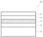
- FIG. 1 shows a schematic cross-sectional view of a pn junction solar cell 100 according to an embodiment of the present invention.
- a pn junction solar cell 100 includes a transparent substrate 10, a transparent conductive film 12 provided on the transparent substrate 10, a p-type semiconductor layer 14 formed of the semiconductor film of the present invention on the transparent conductive film 12, and p An n-type semiconductor layer 16 and a metal electrode 18 provided on the n-type semiconductor layer 16 are stacked on the type semiconductor layer 14.
- the p-type semiconductor layer 14 and the n-type semiconductor layer 16 are laminated adjacent to each other, a pn junction solar cell can be obtained.
- the transparent substrate 10 the same material as the substrate used in the method for producing a semiconductor film of the present invention can be used as long as it is transparent. Specifically, a glass substrate, a resin substrate, etc. are mentioned.
- the transparent conductive film 12 includes a film composed of In 2 O 3 : Sn (ITO), SnO 2 : Sb, SnO 2 : F, ZnO: Al, ZnO: F, CdSnO 4 and the like. .
- the n-type semiconductor layer 16 is preferably a metal oxide. Specific examples include metal oxides containing at least one of Ti, Zn, Sn, and In, and more specific examples include TiO 2 , ZnO, SnO 2 , and IGZO.
- the n-type semiconductor layer is preferably formed by a wet method (also referred to as a liquid phase method) in the same manner as the p-type semiconductor layer from the viewpoint of manufacturing cost.
- a wet method also referred to as a liquid phase method
- the metal electrode 18 Pt, Al, Cu, Ti, Ni, or the like can be used.
- PbS particle dispersion 1 a PbS particle dispersion in which PbS particles were dispersed in toluene was prepared.
- PbS core Evidot nominal particle size 3.3 nm, 20 mg / ml, solvent toluene
- 2 ml of the PbS particle dispersion was taken into the centrifuge tube, 38 ⁇ l of oleic acid was added, and then 20 ml of toluene was added to dilute the concentration of the dispersion.
- the obtained dispersion was concentrated using a rotary evaporator (35 hpa, 40 ° C.), and as a result, about 4 ml of semiconductor quantum dot dispersion 1 (octane solvent) having a concentration of about 10 mg / ml was obtained.
- the particle size of the PbS particles contained in the semiconductor quantum dot dispersion 1 was measured with a STEM (Scanning Transmission Electron Microscope) and analyzed with image confirmation software, the average particle size was 3.2 nm. .
- the product was taken out from the three-necked round bottom flask, and unreacted products and by-products were removed by centrifugation using a centrifuge.
- the product (InP particles) was purified using ultra-dehydrated toluene as a good solvent and dehydrated ethanol as a poor solvent. Specifically, the process of dissolving the product in a good solvent, redispersing the dissolved InP particles in a poor solvent, and centrifuging the resulting InP particle dispersion was repeated. An ultrasonic cleaner was used for redispersion. After repeated centrifugation of the InP particle dispersion, dehydrated ethanol remaining in the InP particle dispersion was removed by distillation under reduced pressure using a rotary evaporator.
- the extracted InP particles were dispersed in octane to obtain an octane dispersion having an oleylamine-modified InP particle concentration of 1 mg / ml. This was designated as semiconductor quantum dot dispersion 2.
- the average particle diameter was about 4 nm.
- a substrate having 65 pairs of comb-shaped platinum electrodes shown in FIG. 2 on a quartz glass was prepared.
- a comb-type platinum electrode (model number 012126, electrode interval 5 ⁇ m) manufactured by BAS was used.
- Table 1 shows the combinations of the semiconductor quantum dot dispersion liquid and the ligand solution in Examples and Comparative Examples.
- PbS in the “seed” column of the “semiconductor quantum dot” column means that the semiconductor quantum dot dispersion liquid 1 was used
- InP means that the semiconductor quantum dot dispersion liquid 2 was used.
- the types of ligands contained in the ligand solution are the ligands shown in the “Compound Name” column of the “Ligand” column of Table 1.
- the ligand (CTAB) used in Comparative Example 5 is cetyltrimethylammonium bromide [(CH 3 (CH 2 ) 15 N (CH 3 ) 3 ) + , Br ⁇ ].
- CTAB cetyltrimethylammonium bromide
- the electrical conductivity of the semiconductor film was evaluated by using a semiconductor parameter analyzer for the produced semiconductor film device. First, the voltage applied to the electrodes was swept between ⁇ 5 to 5 V without irradiating the semiconductor film device with light, and the IV characteristics in the dark state were obtained. The current value with a +5 V bias applied was adopted as the dark current value Id. Next, to evaluate the photocurrent values while irradiating monochromatic light (irradiation intensity 10 13 photons) to the semiconductor film device. The semiconductor film device was irradiated with monochrome light using the apparatus shown in FIG. The wavelength of the monochromatic light was systematically changed between 280 nm and 700 nm. The increase in current from the dark current when irradiating light with a wavelength of 280 nm was taken as the photocurrent value Ip. The evaluation results are shown in Table 1.
- the oleic acid ligand coordinated to the semiconductor quantum dot is subjected to ligand exchange, and the ligand represented by the general formula (A) is coordinated to the semiconductor quantum dot.
- the ligand represented by the general formula (A) is coordinated to the semiconductor quantum dot.
- the electrical conductivity of the semiconductor film is improved by bringing the semiconductor quantum dots close to each other using a specific ligand. can do.
- the semiconductor quantum dots are too close to each other, the semiconductor quantum dots are likely to be aggregated.
- Semiconductor quantum dots are expected to become bulky when aggregated.
- the semiconductor film desirably retains physical properties as a semiconductor quantum dot while exhibiting good electrical characteristics. In particular, when considering application of a semiconductor film to an LED or a solar cell, it is difficult to obtain absorption and emission of a target wavelength unless the semiconductor film has physical properties as a semiconductor quantum dot.
- the film of Comparative Example 7 was obtained in Example 1 without performing the steps (2) and (3) among the steps (1) to (4) in “Manufacturing the semiconductor film”. It is a membrane. Note that the film of Comparative Example 7 was an insulating film that did not exhibit electrical conductivity because the semiconductor quantum dots were not close to each other.
- FIG. 1 The configuration of the experimental setup used for the photoluminescence measurement is schematically shown in FIG.
- This experimental apparatus mainly includes a laser irradiator 20, a total reflection mirror 22, a dichroic mirror 24, lenses 26 and 28, and a spectroscope 32.
- the laser light emitted from the laser irradiator 20 is converted into a total reflection mirror 22,
- the structure reaches the measurement sample (semiconductor film of the evaluation device) 30 and the spectroscope 32 through the dichroic mirror 24 and the lenses 26 and 28, respectively.
- FIG. 5 shows the PL spectrum.
- the peak wavelengths in each ligand are summarized in Table 2.
- the peak wavelength of the PbS semiconductor quantum dot (Comparative Example 7) in which oleic acid was coordinated without ligand exchange was about 1065 nm.
- the emission wavelength shift is the largest, about 50 nm, and the emission wavelength is shifted to the longer wavelength side. This is considered to be because the confinement potential of the semiconductor quantum dots is reduced and the band gap is effectively reduced due to the closeness of the inter-dot distances of the semiconductor quantum dots by the ligand exchange treatment. It is the largest, and the decrease in the band gap is about 50 meV.
- the emission peak exists at about 3350 nm. Therefore, if the semiconductor quantum dots of the semiconductor film are aggregates, it is considered that the emission peak of the semiconductor film composed of the aggregates of semiconductor quantum dots appears around 3350 nm.
- the PbS bulk is a general II-VI group semiconductor, a single crystal of PbS, a semiconductor having a size larger than 100 nm and having no quantum size effect. Therefore, the semiconductor film of the present invention has reduced semiconductor quantum dot spacing and exhibits good conduction characteristics through the semiconductor quantum dots, while retaining physical properties (such as a band gap) as the semiconductor quantum dots. confirmed.
Landscapes
- Chemical & Material Sciences (AREA)
- Engineering & Computer Science (AREA)
- Organic Chemistry (AREA)
- Materials Engineering (AREA)
- Manufacturing & Machinery (AREA)
- Computer Hardware Design (AREA)
- Microelectronics & Electronic Packaging (AREA)
- Power Engineering (AREA)
- Physics & Mathematics (AREA)
- General Physics & Mathematics (AREA)
- Condensed Matter Physics & Semiconductors (AREA)
- Inorganic Chemistry (AREA)
- Nanotechnology (AREA)
- Crystallography & Structural Chemistry (AREA)
- Thin Film Transistor (AREA)
- Photovoltaic Devices (AREA)
- Electroluminescent Light Sources (AREA)
- Led Devices (AREA)
- Life Sciences & Earth Sciences (AREA)
- Sustainable Development (AREA)
- Sustainable Energy (AREA)
Priority Applications (1)
| Application Number | Priority Date | Filing Date | Title |
|---|---|---|---|
| US14/746,114 US10886421B2 (en) | 2012-12-26 | 2015-06-22 | Semiconductor film, method of producing semiconductor film, solar cell, light-emitting diode, thin film transistor, and electronic device |
Applications Claiming Priority (2)
| Application Number | Priority Date | Filing Date | Title |
|---|---|---|---|
| JP2012282429A JP5964742B2 (ja) | 2012-12-26 | 2012-12-26 | 半導体膜、半導体膜の製造方法、太陽電池、発光ダイオード、薄膜トランジスタ、および、電子デバイス |
| JP2012-282429 | 2012-12-26 |
Related Child Applications (1)
| Application Number | Title | Priority Date | Filing Date |
|---|---|---|---|
| US14/746,114 Continuation US10886421B2 (en) | 2012-12-26 | 2015-06-22 | Semiconductor film, method of producing semiconductor film, solar cell, light-emitting diode, thin film transistor, and electronic device |
Publications (1)
| Publication Number | Publication Date |
|---|---|
| WO2014103584A1 true WO2014103584A1 (ja) | 2014-07-03 |
Family
ID=51020678
Family Applications (1)
| Application Number | Title | Priority Date | Filing Date |
|---|---|---|---|
| PCT/JP2013/081498 Ceased WO2014103584A1 (ja) | 2012-12-26 | 2013-11-22 | 半導体膜、半導体膜の製造方法、太陽電池、発光ダイオード、薄膜トランジスタ、および、電子デバイス |
Country Status (3)
| Country | Link |
|---|---|
| US (1) | US10886421B2 (enExample) |
| JP (1) | JP5964742B2 (enExample) |
| WO (1) | WO2014103584A1 (enExample) |
Families Citing this family (8)
| Publication number | Priority date | Publication date | Assignee | Title |
|---|---|---|---|---|
| JP6008736B2 (ja) * | 2012-12-26 | 2016-10-19 | 富士フイルム株式会社 | 半導体膜、半導体膜の製造方法、太陽電池、発光ダイオード、薄膜トランジスタおよび電子デバイス |
| KR102449686B1 (ko) | 2015-09-18 | 2022-09-30 | 엘지전자 주식회사 | 광 변환 복합체, 이를 포함하는 광 변환 부재, 표시장치 및 발광소자 패키지및 이의 제조방법 |
| JP6959119B2 (ja) * | 2017-12-04 | 2021-11-02 | 信越化学工業株式会社 | 量子ドット及びその製造方法、並びに樹脂組成物、波長変換材料、発光素子 |
| US11050033B2 (en) * | 2018-04-24 | 2021-06-29 | Samsung Electronics Co., Ltd. | Light-emitting film, production method thereof, and a light emitting device including the same |
| WO2021002114A1 (ja) * | 2019-07-01 | 2021-01-07 | 富士フイルム株式会社 | 光検出素子、光検出素子の製造方法およびイメージセンサ |
| JP7405850B2 (ja) * | 2019-07-01 | 2023-12-26 | 富士フイルム株式会社 | 半導体膜、光電変換素子、イメージセンサおよび半導体膜の製造方法 |
| JP7439585B2 (ja) * | 2020-03-13 | 2024-02-28 | artience株式会社 | 光電変換素子及び光電変換層形成用組成物 |
| US20240032412A1 (en) * | 2020-12-25 | 2024-01-25 | Boe Technology Group Co., Ltd. | Quantum dot material, light-emitting device and manufacturing method therefor, and display apparatus |
Citations (5)
| Publication number | Priority date | Publication date | Assignee | Title |
|---|---|---|---|---|
| JP2002525394A (ja) * | 1998-09-18 | 2002-08-13 | マサチューセッツ インスティテュート オブ テクノロジー | 水溶性蛍光半導体ナノ結晶 |
| JP2009509129A (ja) * | 2005-08-25 | 2009-03-05 | エドワード・サージェント | 高利得及び高感度の量子ドット光学デバイス及びその作製方法 |
| JP2011513508A (ja) * | 2008-02-25 | 2011-04-28 | ナノコ テクノロジーズ リミテッド | 半導体ナノ粒子キャッピング剤 |
| WO2011074492A1 (ja) * | 2009-12-18 | 2011-06-23 | 株式会社 村田製作所 | 薄膜形成方法、及び量子ドットデバイス |
| US20120031490A1 (en) * | 2010-08-03 | 2012-02-09 | Honeywell International Inc. | Quantum dot solar cells and methods for manufacturing such solar cells |
Family Cites Families (13)
| Publication number | Priority date | Publication date | Assignee | Title |
|---|---|---|---|---|
| EP1116036B1 (en) | 1998-09-18 | 2004-08-11 | Massachusetts Institute Of Technology | Water-soluble fluorescent semiconductor nanocrystals |
| US7663057B2 (en) * | 2004-02-19 | 2010-02-16 | Nanosolar, Inc. | Solution-based fabrication of photovoltaic cell |
| CA2642169A1 (en) * | 2006-02-16 | 2007-08-30 | Solexant Corporation | Nanoparticle sensitized nanostructured solar cells |
| US8643058B2 (en) * | 2006-07-31 | 2014-02-04 | Massachusetts Institute Of Technology | Electro-optical device including nanocrystals |
| US20120125781A1 (en) * | 2008-12-10 | 2012-05-24 | Zhang jin zhong | Compositions and methods for synthesis of hydrogen fuel |
| WO2011109660A2 (en) * | 2010-03-04 | 2011-09-09 | Lockheed Martin Corporation | Compositions containing tin nanoparticles and methods for use thereof |
| GB201005601D0 (en) * | 2010-04-01 | 2010-05-19 | Nanoco Technologies Ltd | Ecapsulated nanoparticles |
| GB201010831D0 (en) * | 2010-06-28 | 2010-08-11 | Ct Angewandte Nanotech Can | A micellular combination comprising a nanoparticle and a plurality of surfmer ligands |
| WO2012071107A1 (en) * | 2010-11-23 | 2012-05-31 | Qd Vision, Inc. | Device including semiconductor nanocrystals & method |
| WO2012112821A1 (en) * | 2011-02-16 | 2012-08-23 | Sandia Solar Technologies Llc | Solar absorbing films with enhanced electron mobility and methods of their preparation |
| KR20130067137A (ko) * | 2011-12-13 | 2013-06-21 | 삼성전자주식회사 | 양자점-매트릭스 박막 및 그의 제조방법 |
| US20140102536A1 (en) * | 2012-03-16 | 2014-04-17 | Nanosensing Technologies, Inc. | Composite Metallic Solar Cells |
| JP2015537378A (ja) * | 2012-10-26 | 2015-12-24 | リサーチ トライアングル インスティテュート | 溶液プロセスによる量子ドットを利用した中間帯半導体、ヘテロ接合、及び光電子デバイス、並びに関連する方法 |
-
2012
- 2012-12-26 JP JP2012282429A patent/JP5964742B2/ja active Active
-
2013
- 2013-11-22 WO PCT/JP2013/081498 patent/WO2014103584A1/ja not_active Ceased
-
2015
- 2015-06-22 US US14/746,114 patent/US10886421B2/en active Active
Patent Citations (5)
| Publication number | Priority date | Publication date | Assignee | Title |
|---|---|---|---|---|
| JP2002525394A (ja) * | 1998-09-18 | 2002-08-13 | マサチューセッツ インスティテュート オブ テクノロジー | 水溶性蛍光半導体ナノ結晶 |
| JP2009509129A (ja) * | 2005-08-25 | 2009-03-05 | エドワード・サージェント | 高利得及び高感度の量子ドット光学デバイス及びその作製方法 |
| JP2011513508A (ja) * | 2008-02-25 | 2011-04-28 | ナノコ テクノロジーズ リミテッド | 半導体ナノ粒子キャッピング剤 |
| WO2011074492A1 (ja) * | 2009-12-18 | 2011-06-23 | 株式会社 村田製作所 | 薄膜形成方法、及び量子ドットデバイス |
| US20120031490A1 (en) * | 2010-08-03 | 2012-02-09 | Honeywell International Inc. | Quantum dot solar cells and methods for manufacturing such solar cells |
Also Published As
| Publication number | Publication date |
|---|---|
| JP5964742B2 (ja) | 2016-08-03 |
| US20150318421A1 (en) | 2015-11-05 |
| JP2014127563A (ja) | 2014-07-07 |
| US10886421B2 (en) | 2021-01-05 |
Similar Documents
| Publication | Publication Date | Title |
|---|---|---|
| JP6177515B2 (ja) | 半導体膜、半導体膜の製造方法、太陽電池、発光ダイオード、薄膜トランジスタ、および、電子デバイス | |
| JP5995661B2 (ja) | 半導体膜、半導体膜の製造方法、太陽電池、発光ダイオード、薄膜トランジスタおよび電子デバイス | |
| JP5964742B2 (ja) | 半導体膜、半導体膜の製造方法、太陽電池、発光ダイオード、薄膜トランジスタ、および、電子デバイス | |
| JP5964744B2 (ja) | 半導体膜の製造方法 | |
| JP5955305B2 (ja) | 半導体膜、半導体膜の製造方法、太陽電池、発光ダイオード、薄膜トランジスタ、および、電子デバイス | |
| Shen et al. | High-performance broadband photodetector based on monolayer MoS2 hybridized with environment-friendly CuInSe2 quantum dots | |
| Ji et al. | 1, 2-Ethanedithiol treatment for AgIn5S8/ZnS quantum dot light-emitting diodes with high brightness | |
| Zhu et al. | Deep-red emitting zinc and aluminium co-doped copper indium sulfide quantum dots for luminescent solar concentrators | |
| Zhang et al. | Antimonene quantum dot-based solid-state solar cells with enhanced performance and high stability | |
| JP6008736B2 (ja) | 半導体膜、半導体膜の製造方法、太陽電池、発光ダイオード、薄膜トランジスタおよび電子デバイス | |
| Sun et al. | Double electron transport layer and optimized CsPbI3 nanocrystal emitter for efficient perovskite light-emitting diodes | |
| JP6086721B2 (ja) | 半導体膜、半導体膜の製造方法、太陽電池、発光ダイオード、薄膜トランジスタ、および、電子デバイス | |
| Bashir et al. | A low-temperature solution-processed indium incorporated zinc oxide electron transport layer for high-efficiency lead sulfide colloidal quantum dot solar cells | |
| CN113410320A (zh) | 一种宽光谱响应光电探测器及其制备方法 | |
| Paliwal et al. | Microwave-polyol synthesis of sub-10-nm PbS nanocrystals for metal oxide/nanocrystal heterojunction photodetectors | |
| Gao et al. | Free radical-resistant carbon dots for bulky luminescent solar concentrators with high optical efficiency | |
| Thomas et al. | An inverted ZnO/P3HT: PbS bulk-heterojunction hybrid solar cell with a CdSe quantum dot interface buffer layer | |
| Gao et al. | Green synthesis of highly efficient CdSe quantum dots for quantum-dots-sensitized solar cells | |
| Kong et al. | AgIn5S8/ZnS Quantum Dots for Luminescent Down-Shifting and Antireflective Layer in Enhancing Photovoltaic Performance | |
| JP6275441B2 (ja) | 半導体膜、酸化物微粒子分散液、半導体膜の製造方法、及び、薄膜トランジスタ | |
| Jabeen et al. | Merocyanine-540 grafted on ZnS and CdS nanocrystals-an approach for enhancing the efficiency of inorganic-organic hybrid solar cell | |
| Alalousi et al. | The effect of Cu/In molar ratio on the analysis and characterization of CuInS2 nanostructures | |
| Taylor et al. | Colloidal quantum dots solar cells | |
| Tulsani et al. | Inorganic metal iodide mediated solution phase surface passivation for quantum dot solar cell | |
| CN115148907B (zh) | 一种基于非宽禁带钙钛矿的紫外光电探测器及其制备方法 |
Legal Events
| Date | Code | Title | Description |
|---|---|---|---|
| 121 | Ep: the epo has been informed by wipo that ep was designated in this application |
Ref document number: 13869636 Country of ref document: EP Kind code of ref document: A1 |
|
| NENP | Non-entry into the national phase |
Ref country code: DE |
|
| 122 | Ep: pct application non-entry in european phase |
Ref document number: 13869636 Country of ref document: EP Kind code of ref document: A1 |