WO2014103430A1 - Système de transmission de puissance sans fil - Google Patents
Système de transmission de puissance sans fil Download PDFInfo
- Publication number
- WO2014103430A1 WO2014103430A1 PCT/JP2013/073610 JP2013073610W WO2014103430A1 WO 2014103430 A1 WO2014103430 A1 WO 2014103430A1 JP 2013073610 W JP2013073610 W JP 2013073610W WO 2014103430 A1 WO2014103430 A1 WO 2014103430A1
- Authority
- WO
- WIPO (PCT)
- Prior art keywords
- power transmission
- power
- voltage
- transmission system
- power receiving
- Prior art date
Links
- 230000005540 biological transmission Effects 0.000 title claims abstract description 165
- 239000003990 capacitor Substances 0.000 claims abstract description 34
- 230000008859 change Effects 0.000 claims abstract description 14
- 239000004065 semiconductor Substances 0.000 claims abstract description 10
- 230000005674 electromagnetic induction Effects 0.000 claims description 3
- 238000009499 grossing Methods 0.000 claims description 3
- 230000015556 catabolic process Effects 0.000 abstract 1
- 238000006731 degradation reaction Methods 0.000 abstract 1
- 238000010168 coupling process Methods 0.000 description 23
- 230000008878 coupling Effects 0.000 description 21
- 238000005859 coupling reaction Methods 0.000 description 21
- 238000001514 detection method Methods 0.000 description 21
- 238000010586 diagram Methods 0.000 description 20
- 238000004891 communication Methods 0.000 description 11
- 230000005856 abnormality Effects 0.000 description 10
- 230000005684 electric field Effects 0.000 description 7
- 230000002159 abnormal effect Effects 0.000 description 2
- 238000000034 method Methods 0.000 description 2
- 230000004075 alteration Effects 0.000 description 1
- 230000001413 cellular effect Effects 0.000 description 1
- 230000007423 decrease Effects 0.000 description 1
- 230000004907 flux Effects 0.000 description 1
Images


Classifications
-
- H—ELECTRICITY
- H04—ELECTRIC COMMUNICATION TECHNIQUE
- H04B—TRANSMISSION
- H04B5/00—Near-field transmission systems, e.g. inductive or capacitive transmission systems
- H04B5/70—Near-field transmission systems, e.g. inductive or capacitive transmission systems specially adapted for specific purposes
- H04B5/79—Near-field transmission systems, e.g. inductive or capacitive transmission systems specially adapted for specific purposes for data transfer in combination with power transfer
-
- H—ELECTRICITY
- H02—GENERATION; CONVERSION OR DISTRIBUTION OF ELECTRIC POWER
- H02J—CIRCUIT ARRANGEMENTS OR SYSTEMS FOR SUPPLYING OR DISTRIBUTING ELECTRIC POWER; SYSTEMS FOR STORING ELECTRIC ENERGY
- H02J50/00—Circuit arrangements or systems for wireless supply or distribution of electric power
- H02J50/05—Circuit arrangements or systems for wireless supply or distribution of electric power using capacitive coupling
-
- H—ELECTRICITY
- H02—GENERATION; CONVERSION OR DISTRIBUTION OF ELECTRIC POWER
- H02J—CIRCUIT ARRANGEMENTS OR SYSTEMS FOR SUPPLYING OR DISTRIBUTING ELECTRIC POWER; SYSTEMS FOR STORING ELECTRIC ENERGY
- H02J50/00—Circuit arrangements or systems for wireless supply or distribution of electric power
- H02J50/10—Circuit arrangements or systems for wireless supply or distribution of electric power using inductive coupling
- H02J50/12—Circuit arrangements or systems for wireless supply or distribution of electric power using inductive coupling of the resonant type
-
- H—ELECTRICITY
- H02—GENERATION; CONVERSION OR DISTRIBUTION OF ELECTRIC POWER
- H02J—CIRCUIT ARRANGEMENTS OR SYSTEMS FOR SUPPLYING OR DISTRIBUTING ELECTRIC POWER; SYSTEMS FOR STORING ELECTRIC ENERGY
- H02J7/00—Circuit arrangements for charging or depolarising batteries or for supplying loads from batteries
- H02J7/007—Regulation of charging or discharging current or voltage
- H02J7/00712—Regulation of charging or discharging current or voltage the cycle being controlled or terminated in response to electric parameters
Definitions
- the present invention relates to a wireless power transmission system that enables data communication from a power receiving apparatus to a power transmitting apparatus.
- a magnetic field coupling type power transmission system in which power is transmitted from a primary coil of a power transmission apparatus to a secondary coil of a power reception apparatus using a magnetic field.
- this system when electric power is transmitted by magnetic coupling, since the magnitude of magnetic flux passing through each coil greatly affects the electromotive force, high accuracy is required for the relative positional relationship between the primary coil and the secondary coil. Moreover, since the coil is used, it is difficult to reduce the size of the apparatus.
- Patent Document 1 an electric field coupling type wireless power transmission system as disclosed in Patent Document 1 has also been proposed.
- power is transmitted from the coupling electrode of the power transmission apparatus to the coupling electrode of the power reception apparatus via an electric field.
- the required accuracy of the relative position of the coupling electrode is relatively loose, and the coupling electrode can be made smaller and thinner.
- the power transmission device described in Patent Document 1 includes a high-frequency high-voltage generation circuit, a passive electrode, and an active electrode.
- the power receiving device includes a high-frequency high-voltage load circuit, a passive electrode, and an active electrode. Then, when the active electrode of the power transmission device and the active electrode of the power reception device come close to each other with a distance, the two electrodes are electrically coupled.
- the passive electrode of the power transmission device, the active electrode of the power transmission device, the active electrode of the power reception device, and the passive electrode of the power reception device are arranged in parallel to each other.
- this wireless power transmission system it may be necessary to perform data communication between the power transmission device and the power reception device and transmit the status of the power reception device (for example, the amount of charge) to the power transmission device.
- the status of the power reception device for example, the amount of charge
- a method of modulating the AC voltage or AC current transmitted between the power transmitting device and the power receiving device and performing communication simultaneously with the power transmission can be considered.
- an object of the present invention is to provide a wireless power transmission system that enables data communication between a power transmission device and a power reception device without suppressing fluctuations in output voltage due to load modulation and without reducing power transmission efficiency. is there.
- a wireless power transmission system includes a power transmission device that applies an AC voltage converted from an input DC voltage to a power transmission unit, and an AC voltage that is induced in the power reception unit when the AC voltage is applied to the power transmission unit.
- a power receiving device that converts the current into a DC voltage by rectification and smoothing, and the power receiving device includes first and second diodes having anodes connected to each other, and a third power source having cathodes connected to each other.
- a diode bridge composed of a fourth diode and a first series circuit comprising a semiconductor switch element and a capacitor connected in parallel to each of the first and second diodes, or the third and fourth diodes At least one of a second series circuit including a semiconductor switch element and a capacitor connected in parallel to each other, and the semiconductor A control means for inputting a modulation signal to the control terminal of the switching element, wherein the power transmitting apparatus is characterized by having a signal reading means for reading the modulated signal based on a change of the transmission current.
- the weight of the load on the power receiving device side can be changed by simultaneously turning on and off the semiconductor switches of the first and second series circuits.
- the power receiving device changes the weight of the load according to the data to be transmitted to the power transmission device, and changes the power transmission current in the power transmission device. For example, when data “1” is transmitted to the power transmission device, the load on the power receiving device side is set to a high load state, and when data “0” is transmitted, the load is set to a low load state. Then, the data “1” and “0” are discriminated by reading the change in the transmission current with the power transmission device and detecting the change in the load state on the power reception device side. Thereby, data communication by load modulation from the power receiving apparatus to the power transmitting apparatus is possible. In this case, it is possible to suppress the fluctuation of the output voltage and improve the power transmission efficiency as compared with the case of the conventional resistance load modulation.
- the power transmission device preferably includes a DC-AC inverter and a booster circuit that boosts an AC voltage converted by the DC-AC inverter and applies the boosted voltage to the power transmission unit.
- the signal reading unit detects a change in the transmission current from a change in the current input to the power transmission device. In this configuration, since a modulation signal is read from a change in direct current, complicated signal processing is not required.
- the power receiving device may include both the first series circuit and the second series circuit.
- data of four states (00, 01, 10, 11) can be generated by the power receiving device, and information can be transmitted from the power receiving device to the power transmitting device at a high rate.
- the power transmission unit includes a power transmission side active electrode and a power transmission side passive electrode
- the power reception unit includes a power reception side active electrode opposed to the power transmission side active electrode via a gap, and the power transmission side passive electrode via a gap.
- Power receiving side passive electrode that is opposed to or directly in contact with each other, and the power transmission side active electrode and the power receiving side active electrode are opposed to each other and are electrically coupled to transmit power from the power transmission device to the power receiving device. It may be configured.
- the power transmission unit has a power transmission side coil through which a high frequency current is passed, the power reception unit has a power reception side coil in which a high frequency current is induced by electromagnetic induction, and the power transmission side coil and the power reception side coil are magnetically coupled. By doing so, the power transmission from the power transmission device to the power reception device may be adopted.
- FIG. 1 is a circuit diagram of a wireless power transmission system according to a first embodiment.
- Schematic diagram of wireless power transmission system Block diagram for explaining a controller of a power transmission device
- the figure which shows the voltage waveform and current waveform when the drive frequency of a wireless power transmission system is 255 kHz
- the figure which shows the voltage waveform and electric current waveform when the drive frequency of a wireless power transmission system is 295 kHz
- Circuit diagram of wireless power transmission system according to Embodiment 2 Schematic diagram of wireless power transmission system Circuit diagram of another example of the wireless power transmission system according to the second embodiment Circuit diagram of wireless power transmission system according to Embodiment 3
- FIG. 1 is a circuit diagram of a wireless power transmission system according to the first embodiment.
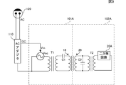
- FIG. 2 is a schematic diagram of a wireless power transmission system.
- a wireless power transmission system 100 includes a power transmission device 101 and a power reception device 102.
- the power receiving apparatus 102 includes a load RL.
- This load RL is a secondary battery.
- the power receiving apparatus 102 is, for example, a portable electronic device that includes the secondary battery. Examples of portable electronic devices include cellular phones, PDAs (Personal Digital Assistants), portable music players, notebook PCs, and digital cameras.
- the power transmission apparatus 101 is a charging stand on which the power reception apparatus 102 is mounted and charges a secondary battery of the power reception apparatus 102.
- the power transmission apparatus 101 is connected to a power source 120 via an AC adapter 110 as shown in FIG.
- the power source 120 is, for example, a household outlet of AC 100V to 230V.
- the AC adapter 110 converts AC 100V to 230V into DC 5V or 12V and outputs it to the power transmission apparatus 101.
- the power transmission apparatus 101 operates using the input DC voltage Vin as a power source.
- the power transmission apparatus 101 converts the DC voltage Vin into the AC voltage Vac and boosts it with the step-up transformer T1.
- the power transmission apparatus 101 applies the boosted AC voltage between the active electrode 14 and the passive electrode 15.
- the frequency of this AC voltage is 100 kHz to 10 MHz.
- the power receiving apparatus 102 includes an active electrode 24 and a passive electrode 25.
- the active electrode 24 and the passive electrode 25 face the active electrode 14 and the passive electrode 15 of the power transmission device 101 with a gap when the power receiving device 102 is placed on the power transmission device 101.
- the passive electrodes 15 and 25 may be in direct contact.
- a voltage is applied between the active electrode 14 and the passive electrode 15, an electric field is generated between the active electrodes 14 and 24 that are arranged to face each other, and electric power is transmitted from the power transmitting apparatus 101 to the power receiving apparatus 102 via this electric field.
- the power receiving apparatus 102 steps down an AC voltage induced by power transmission by the step-down transformer T2, applies the voltage to the secondary side circuit 20A, and rectifies and smoothes the secondary side circuit 20A.
- the input terminals IN1 and IN2 of the power transmission apparatus 101 are connected to DCs composed of switching elements Q1, Q2, Q3, and Q4 via current detection resistors R1 and voltage detection voltage dividing resistors R2 and R3.
- -AC inverter circuit is connected.
- the switch elements Q1, Q2, Q3 and Q4 are n-type MOS-FETs. Switch elements Q1 and Q2 are connected in series, and switch elements Q3 and Q4 are connected in series.
- a primary coil of the step-up transformer T1 is connected to a connection point between the switch elements Q1 and Q2 and a connection point between the switch elements Q3 and Q4.
- the switch elements Q1, Q2, Q3, and Q4 are supplied with a control signal from the driver 11 to the gate.
- the driver 11 alternately turns on and off the switch elements Q1 and Q4 and the switch elements Q2 and Q3 in accordance with a drive signal from the controller 10.
- An active electrode 14 and a passive electrode 15 are connected to the secondary coil of the step-up transformer T1, and an AC voltage boosted by the step-up transformer T1 is applied to the active electrode 14 and the passive electrode 15. Further, a capacitor C1 is connected in parallel to the secondary coil, and the capacitor C1 forms a series resonance circuit with the leakage inductor L leak of the step-up transformer T1.
- the controller 10 detects a power transmission current and a power transmission voltage in the power transmission device 101, determines whether power transmission is possible, and generates a control signal for the driver 11. Further, the transmission power is changed by changing the duty ratio of the switch elements Q1 to Q4. The controller 10 will be described in detail later.
- the primary coil of the step-down transformer T2 is connected to the active electrode 24 and the passive electrode 25 of the power receiving apparatus 102.
- a capacitor C2 is connected in parallel to the primary coil to form a parallel resonance circuit.
- a diode bridge formed of diodes D1, D2, D3, and D4 is connected to the secondary coil of the step-down transformer T2.
- the diode D1 has a cathode connected to the anode of the diode D4 and an anode connected to the anode of the diode D2.
- the cathode of the diode D4 is connected to the cathode of the diode D3, and the cathode of the diode D2 is connected to the anode of the diode D3.
- the connection points of the diodes D1, D4 and the connection points of the diodes D2, D3 are connected to the secondary coil of the step-down transformer T2.
- connection point of the diodes D3 and D4 is connected to the output terminal OUT1 via the smoothing capacitor C3 and the DC-DC converter 20.
- a connection point between the diodes D1 and D2 is connected to the output terminal OUT2.
- a load RL that is a secondary battery is connected to the output terminals OUT1 and OUT2.
- the power receiving apparatus 102 includes a communication circuit for performing data transmission from the power receiving apparatus 102 to the power transmitting apparatus 101.
- the communication circuit includes switch elements Q5 and Q6, capacitors Ca and Cb, and a driver circuit 21.
- the switch elements Q5 and Q6 are n-type MOS-FETs.
- the switch element Q5 has a drain connected to a connection point between the diodes D1 and D4 via the capacitor Ca, and a source connected to a connection point between the diodes D1 and D2.
- the switch element Q6 has a source connected to a connection point between the diodes D1 and D2, and a drain connected to a connection point between the diodes D2 and D3 via the capacitor Cb. That is, the series circuit of the capacitor Ca and the switch element Q5 is connected in parallel to the diode D1, and the series circuit of the capacitor Cb and the switch element Q6 is connected in parallel to the diode D2.
- the series circuit of the capacitor Ca and the switch element Q5 and the series circuit of the capacitor Cb and the switch element Q6 correspond to the “first series circuit” according to the present invention.
- the gates of the switch elements Q5 and Q6 are connected to the control circuit (control means of the present invention) 30 via the driver circuit 21.
- the control circuit 30 detects the current flowing through the DC-DC converter 20 and the voltage output from the output terminals OUT1 and OUT2, and detects the state of the power receiving apparatus 102, for example, the charging capacity of the secondary battery. And the control circuit 30 produces
- the output modulation signal is applied to the gates of the switch elements Q5 and Q6 via the driver circuit 21, and the switch elements Q5 and Q6 are simultaneously turned on and off.
- the diodes D1 and D2 are bypassed by the capacitors Ca and Cb, and when the switch elements Q5 and Q6 are simultaneously turned off, the diodes are opened. That is, the load impedance as viewed from the power transmitting apparatus 101 side on the power receiving apparatus 102 side is changed by turning on and off the switch elements Q5 and Q6.
- binary data is transmitted from the power receiving apparatus 102 to the power transmitting apparatus 101.
- the load impedance viewed from the power transmitting apparatus 101 side on the power receiving apparatus 102 side is set to the first state (for example, H level), and data “0” is transmitted.
- the second state for example, L level
- the first state for example, the power transmission current in the power transmission device 101 increases, and in the case of the second state, the power transmission current in the power transmission device 101 decreases.
- the controller 10 can determine the data “1” and “0” by reading the transmission current, that is, the change in the direct current input from the input terminal IN1. Thereby, the controller 10 acquires information transmitted from the power receiving apparatus 102, for example, information such as the charging capacity of the secondary battery.
- FIG. 3 is a block diagram for explaining the controller 10 of the power transmission apparatus 101.
- the controller 10 includes an IDC detection unit 10A, a signal reading unit 10B, a VAC detection unit 10C, a Vin detection unit 10D, and an abnormality determination unit 10E.
- the IDC detection unit 10A detects the direct current IDC. Specifically, the IDC detection unit 10A detects a direct current input from the input terminal IN1 based on the voltage across the resistor R1.
- the signal reading unit 10B reads the value of the direct current IDC detected by the IDC detection unit 10A.
- the direct current IDC changes according to on / off of the switch elements Q5 and Q6 on the power receiving apparatus 102 side.
- the signal reading unit 10B reads binary data created on the power receiving device 102 side from the change, and reads information transmitted from the power receiving device 102, for example, information such as the charging capacity of the secondary battery. Since the signal reading unit 10B reads data transmitted from the change in the direct current IDC, the controller 10 does not require complicated signal processing.
- VAC detection unit 10C detects the transmission voltage VAC.
- the Vin detection unit 10D detects the DC voltage Vin input from the input terminals IN1 and IN2.
- the abnormality determination unit 10E detects an abnormality of the system based on the transmission voltage VAC detected by the VAC detection unit 10C and the DC voltage Vin detected by the Vin detection unit 10D. For example, when an abnormal object is placed on the power transmission device 101, the abnormality determination unit 10E determines that there is an abnormality from the amount of change in the transmission voltage VAC.
- the controller 10 adjusts the generation of the PWM signal based on the information read by the signal reading unit 10B or the determination result by the abnormality determination unit 10E, and outputs the PWM signal to the driver 11 so that the switching elements Q1 to Q4 Switching control is performed or the operation of the driver 11 is stopped, the switch elements Q1 to Q4 are turned off, and power transmission is stopped.
- FIG. 4 is a diagram showing a voltage waveform and a current waveform in the first embodiment.
- the waveforms of the output voltage of the diode bridge, the gate / source voltages of the switching elements Q5 and Q6, and the DC current IDC are shown in order from the top.
- the waveform of the direct current IDC is a modulation waveform close to a square wave.
- the controller 10 reads the binary data created on the power receiving apparatus 102 side by detecting the modulated DC current IDC. Further, even when the switch elements Q5 and Q6 are turned on / off, the ripple in the output voltage from the diode bridge is small.
- a resonance circuit is provided on the power transmission device 101 side, a resonance circuit is provided on the power reception device 102 side, capacitively coupled to each other, and operated near the center of the coupled resonance frequency (natural frequency), and the resonance circuit.
- the modulation section including the load circuit and the load circuit are separated from each other by a diode bridge.
- data communication from the power receiving apparatus 102 to the power transmitting apparatus 101 can be performed while power is supplied while suppressing a ripple component of the output voltage.
- FIG. 4 described above is a diagram illustrating a voltage waveform and a current waveform when the resonance frequency on the power receiving apparatus 102 side is set to the drive frequency 275 kHz of the wireless power transmission system 100.
- FIG. 5 is a diagram illustrating a voltage waveform and a current waveform when the driving frequency of the wireless power transmission system 100 is 255 kHz.
- FIG. 6 is a diagram illustrating a voltage waveform and a current waveform when the drive frequency of the wireless power transmission system 100 is 295 kHz.
- the resonance frequency on the power receiving apparatus 102 side is set to the driving frequency of the wireless power transmission system 100, the output voltage is higher than the others. Furthermore, when the drive frequency is lower than the resonance frequency (FIG. 5), the modulation degree deteriorates. Therefore, the resonance frequency on the power receiving apparatus 102 side is preferably set to the drive frequency of the wireless power transmission system 100.
- FIG. 7 is a diagram showing a voltage waveform and a current waveform when only one series circuit of the switch element Q6 and the capacitor Cb is provided.
- FIG. 7 shows the waveforms of the output voltage of the diode bridge, the gate-source voltage of the switch element Q5, and the direct current IDC in order from the top.
- a bypass path by the capacitor Ca is formed via the diode D1, and no bypass path is formed for the diode D2. Therefore, when the switch element Q5 is turned on, one of the rectifying actions is lost, and as shown in FIG. 7, the waveform of the direct current IDC becomes asymmetric and the output voltage ripple also increases.
- a series circuit of a switch element and a capacitor is connected in parallel to each of the two diodes D1 and D2 of the diode bridge, and the switch elements are simultaneously turned on / off.
- data can be transmitted from the power receiving apparatus 102 to the power transmitting apparatus 101 while reducing a ripple component generated in the output voltage.
- FIG. 8 is a circuit diagram of a wireless power transmission system according to the second embodiment.
- FIG. 9 is a schematic diagram of a wireless power transmission system.
- the wireless power transmission system 100 according to the first embodiment performs power transmission by electric field coupling, whereas the wireless power transmission system 100A according to the second embodiment performs power transmission by magnetic field coupling.
- a power transmission side coupling coil (power transmission side coil of the present invention) 16 is connected to the secondary coil of the step-up transformer T1.
- the power transmission side coupling coil 16 forms a series resonance circuit with the capacitor C1.
- a power receiving side coupling coil (power receiving side coil of the present invention) 26 in which high-frequency current is induced by electromagnetic induction with the power transmitting side coupling coil 16, is connected to the primary coil of the step-down transformer T2. .
- the power receiving side coupling coil 26 forms a parallel resonant circuit with the capacitor C2.
- Other configurations of the power transmitting apparatus 101A and the power receiving apparatus 102A are the same as those in the first embodiment.
- a detection unit for the alternating current IAC of the series resonance circuit is provided and input to the controller 10.
- the controller 10 includes an IAC detection unit in addition to the functional units described in FIG.
- the abnormality determination unit of the controller 10 is detected by the DC current IDC detected by the IDC detection unit or the transmission voltage VAC detected by the VAC detection unit (or the transmission AC current IAC detected by the IAC detection unit) and the Vin detection unit.
- the system abnormality is detected based on the DC voltage Vin. For example, when an abnormal object is placed on the power transmission device, the abnormality determination unit determines that there is an abnormality from the fluctuation amount of the direct current IDC or the fluctuation amount of the transmission voltage VAC (or the fluctuation amount of the transmission AC current IAC).
- the wireless power transmission system 100A also transmits data from the power receiving apparatus 102A to the power transmitting apparatus 101A by simultaneously turning on and off the switch elements Q5 and Q6.
- data transmission can be performed without interrupting power transmission.
- data communication from the power receiving apparatus 102A to the power transmitting apparatus 101A can be performed while reducing ripples generated in the output voltage.
- FIG. 10 is a circuit diagram of another example of the wireless power transmission system 100A according to the second embodiment.
- the power transmission device 101B does not have a step-up transformer, and one end of the power transmission side coupling coil 16 is connected to the switch elements Q1 and Q2 via a capacitor C4 that forms a series resonance circuit. The other end is connected to the connection point of the switch elements Q3 and Q4.
- the power receiving device 102B does not have a step-down transformer, and one end of the power receiving side coupling coil 26 is connected to the connection point of the diodes D1 and D2, and the other end is connected to the connection point of the diodes D3 and D4.
- the power receiving side coupling coil 26 forms a parallel resonant circuit with the capacitor C5.
- FIG. 11 is a circuit diagram of a wireless power transmission system according to the third embodiment.
- the power transmission apparatus 101 included in the wireless power transmission system 100C according to the third embodiment is the same as that of the first embodiment.
- the power receiving device 102C is configured such that a series circuit of the switch element Q7 and the capacitor Cc and a series circuit of the switch element Q8 and the capacitor Cd are respectively connected in parallel to the diodes D2 and D4 of the power receiving device 102 according to the first embodiment. It is a configuration.
- binary data is transmitted from the power receiving apparatus to the power transmitting apparatus, whereas in the third embodiment, four levels (four values) can be transmitted at a high rate. Can be sent.
- the series circuit of the switch element Q7 and the capacitor Cc and the series circuit of the switch element Q8 and the capacitor Cd correspond to the “second series circuit” according to the present invention.
- the switch elements Q7 and Q8 are p-type MOS-FETs, and a modulation signal is applied to the gate from the control circuit 30 via the buffer circuit 22.
- the switch elements Q7 and Q8 may be n-type MOS-FETs. In this case, a bootstrap circuit is provided to drive the switch elements Q7 and Q8.
- FIG. 12 is a diagram showing a voltage waveform and a current waveform in the third embodiment.
- the waveforms of the gate and source voltages of the switching elements Q5 and Q6, the gate and source voltages of the switching elements Q7 and Q8, the output voltage of the diode bridge, and the DC current IDC are shown in order from the top.
- four levels of load modulation are repeated in the switch elements Q5 and Q6 and the switch elements Q7 and Q8, and the waveform of the DC current IDC is a modulation waveform having a four-state square wave.
- the ripple in the output voltage from the diode bridge is small.
- 10-controller (signal reading means) 10A-IDC detection unit 10B-signal reading unit (signal reading means) 10C-VAC detection unit 10D-Vin detection unit 10E-abnormality determination unit 11-driver 14-active electrode (power transmission unit) 15-Passive electrode (power transmission part) 16- Coil for power transmission side coupling (power transmission part, power transmission side coil) 20-DC-DC converter 24-active electrode (power receiving unit) 25-Passive electrode (power receiving unit) 26-Coil for receiving side (power receiving part, coil on receiving side) 30-Control circuit (control means) 100, 100A, 100B, 100C—Wireless power transmission systems 101, 101A, 101B—Power transmission devices 102, 102A, 102B, 102C—Power reception device 110—AC adapter 120—Power sources C1, C2, C3, Ca, Cb, Cc, Cd -Capacitor D1-diode (first diode) D2-diode (second diode) D3-diode (third
Landscapes
- Engineering & Computer Science (AREA)
- Computer Networks & Wireless Communication (AREA)
- Power Engineering (AREA)
- Signal Processing (AREA)
- Charge And Discharge Circuits For Batteries Or The Like (AREA)
Abstract
Priority Applications (3)
| Application Number | Priority Date | Filing Date | Title |
|---|---|---|---|
| CN201390000841.1U CN204517509U (zh) | 2012-12-27 | 2013-09-03 | 无线电力传输系统 |
| JP2014554182A JPWO2014103430A1 (ja) | 2012-12-27 | 2013-09-03 | ワイヤレス電力伝送システム |
| US14/699,010 US20150249483A1 (en) | 2012-12-27 | 2015-04-29 | Wireless power transmission system |
Applications Claiming Priority (2)
| Application Number | Priority Date | Filing Date | Title |
|---|---|---|---|
| JP2012284725 | 2012-12-27 | ||
| JP2012-284725 | 2012-12-27 |
Related Child Applications (1)
| Application Number | Title | Priority Date | Filing Date |
|---|---|---|---|
| US14/699,010 Continuation US20150249483A1 (en) | 2012-12-27 | 2015-04-29 | Wireless power transmission system |
Publications (1)
| Publication Number | Publication Date |
|---|---|
| WO2014103430A1 true WO2014103430A1 (fr) | 2014-07-03 |
Family
ID=51020535
Family Applications (1)
| Application Number | Title | Priority Date | Filing Date |
|---|---|---|---|
| PCT/JP2013/073610 WO2014103430A1 (fr) | 2012-12-27 | 2013-09-03 | Système de transmission de puissance sans fil |
Country Status (4)
| Country | Link |
|---|---|
| US (1) | US20150249483A1 (fr) |
| JP (1) | JPWO2014103430A1 (fr) |
| CN (1) | CN204517509U (fr) |
| WO (1) | WO2014103430A1 (fr) |
Cited By (4)
| Publication number | Priority date | Publication date | Assignee | Title |
|---|---|---|---|---|
| CN106160262A (zh) * | 2015-05-13 | 2016-11-23 | 精工爱普生株式会社 | 控制装置、电子设备以及无触点电力传输系统 |
| CN107210977A (zh) * | 2015-01-20 | 2017-09-26 | 三菱电机株式会社 | 信号传输装置 |
| JP2019511182A (ja) * | 2017-02-24 | 2019-04-18 | クワントン オーピーピーオー モバイル テレコミュニケーションズ コーポレイション リミテッド | 等化回路、充電対象機器及び充電制御方法 |
| JP2022501996A (ja) * | 2018-09-30 | 2022-01-06 | 華為技術有限公司Huawei Technologies Co., Ltd. | ワイヤレス充電受信機回路、制御方法、及び端末デバイス |
Families Citing this family (12)
| Publication number | Priority date | Publication date | Assignee | Title |
|---|---|---|---|---|
| CN204721100U (zh) * | 2012-12-28 | 2015-10-21 | 株式会社村田制作所 | 电力输送系统 |
| CN205304411U (zh) * | 2013-06-05 | 2016-06-08 | 株式会社村田制作所 | 电子装置以及无线电力输送系统 |
| CN104578439B (zh) * | 2013-10-21 | 2018-10-09 | 台达电子企业管理(上海)有限公司 | 用于无线充电线路的装置 |
| US9673658B2 (en) * | 2014-03-06 | 2017-06-06 | Samsung Electro-Mechanics Co., Ltd. | Non-contact capacitive coupling type power charging apparatus and non-contact capacitive coupling type battery apparatus |
| CN105186714A (zh) * | 2015-09-10 | 2015-12-23 | 胡江浩 | 一种低功率无线充电电路拓扑结构 |
| WO2017115625A1 (fr) * | 2015-12-28 | 2017-07-06 | 日本電産株式会社 | Système de corps mobile |
| JPWO2017213032A1 (ja) * | 2016-06-06 | 2019-01-31 | 株式会社村田製作所 | ワイヤレス給電システム、ワイヤレス電力送電装置およびワイヤレス電力受電装置 |
| DE102016210639A1 (de) * | 2016-06-15 | 2017-12-21 | Robert Bosch Gmbh | Ladevorrichtung |
| JP6519574B2 (ja) * | 2016-12-07 | 2019-05-29 | Tdk株式会社 | ワイヤレス受電装置及びこれを用いたワイヤレス電力伝送装置並びに整流器 |
| WO2019189660A1 (fr) * | 2018-03-28 | 2019-10-03 | パナソニックIpマネジメント株式会社 | Module de transmission de courant, module de réception de courant, dispositif de transmission de courant, dispositif de réception de courant et système de transfert de courant sans fil |
| US10998776B2 (en) | 2019-04-11 | 2021-05-04 | Apple Inc. | Wireless power system with in-band communications |
| DE102020109640A1 (de) * | 2019-04-11 | 2020-10-15 | Apple Inc. | Drahtloses leistungssystem mit in-band-kommunikationen |
Citations (2)
| Publication number | Priority date | Publication date | Assignee | Title |
|---|---|---|---|---|
| JP2010288431A (ja) * | 2009-06-15 | 2010-12-24 | Sanyo Electric Co Ltd | 電池内蔵機器と充電台 |
| WO2012086411A1 (fr) * | 2010-12-24 | 2012-06-28 | 株式会社村田製作所 | Système de transmission d'électricité sans fil, dispositif de transmission d'électricité et dispositif de réception d'électricité |
Family Cites Families (5)
| Publication number | Priority date | Publication date | Assignee | Title |
|---|---|---|---|---|
| JP2011109810A (ja) * | 2009-11-17 | 2011-06-02 | Panasonic Electric Works Co Ltd | 非接触給電装置 |
| WO2012101907A1 (fr) * | 2011-01-26 | 2012-08-02 | 株式会社村田製作所 | Système de transmission d'énergie |
| US9350193B2 (en) * | 2011-06-01 | 2016-05-24 | Samsung Electronics Co., Ltd. | Method and apparatus for detecting load fluctuation of wireless power transmission |
| WO2013035392A1 (fr) * | 2011-09-07 | 2013-03-14 | 株式会社村田製作所 | Système de transmission d'énergie et dispositif de transmission d'énergie |
| JP5780894B2 (ja) * | 2011-09-16 | 2015-09-16 | 株式会社半導体エネルギー研究所 | 非接触給電システム |
-
2013
- 2013-09-03 WO PCT/JP2013/073610 patent/WO2014103430A1/fr active Application Filing
- 2013-09-03 JP JP2014554182A patent/JPWO2014103430A1/ja active Pending
- 2013-09-03 CN CN201390000841.1U patent/CN204517509U/zh not_active Expired - Lifetime
-
2015
- 2015-04-29 US US14/699,010 patent/US20150249483A1/en not_active Abandoned
Patent Citations (2)
| Publication number | Priority date | Publication date | Assignee | Title |
|---|---|---|---|---|
| JP2010288431A (ja) * | 2009-06-15 | 2010-12-24 | Sanyo Electric Co Ltd | 電池内蔵機器と充電台 |
| WO2012086411A1 (fr) * | 2010-12-24 | 2012-06-28 | 株式会社村田製作所 | Système de transmission d'électricité sans fil, dispositif de transmission d'électricité et dispositif de réception d'électricité |
Cited By (9)
| Publication number | Priority date | Publication date | Assignee | Title |
|---|---|---|---|---|
| CN107210977A (zh) * | 2015-01-20 | 2017-09-26 | 三菱电机株式会社 | 信号传输装置 |
| CN107210977B (zh) * | 2015-01-20 | 2020-06-26 | 三菱电机株式会社 | 信号传输装置 |
| CN106160262A (zh) * | 2015-05-13 | 2016-11-23 | 精工爱普生株式会社 | 控制装置、电子设备以及无触点电力传输系统 |
| JP2016214024A (ja) * | 2015-05-13 | 2016-12-15 | セイコーエプソン株式会社 | 制御装置、電子機器及び無接点電力伝送システム |
| JP2019511182A (ja) * | 2017-02-24 | 2019-04-18 | クワントン オーピーピーオー モバイル テレコミュニケーションズ コーポレイション リミテッド | 等化回路、充電対象機器及び充電制御方法 |
| US10541541B2 (en) | 2017-02-24 | 2020-01-21 | Guangdong Oppo Mobile Telecommunications Corp., Ltd. | Equalization circuit, device to be charged and charging control method |
| JP2022501996A (ja) * | 2018-09-30 | 2022-01-06 | 華為技術有限公司Huawei Technologies Co., Ltd. | ワイヤレス充電受信機回路、制御方法、及び端末デバイス |
| JP7150156B2 (ja) | 2018-09-30 | 2022-10-07 | 華為技術有限公司 | ワイヤレス充電受信機回路、制御方法、及び端末デバイス |
| US11870293B2 (en) | 2018-09-30 | 2024-01-09 | Huawei Technologies Co., Ltd. | Wireless charging receiver circuit, control method, and terminal device |
Also Published As
| Publication number | Publication date |
|---|---|
| US20150249483A1 (en) | 2015-09-03 |
| JPWO2014103430A1 (ja) | 2017-01-12 |
| CN204517509U (zh) | 2015-07-29 |
Similar Documents
| Publication | Publication Date | Title |
|---|---|---|
| WO2014103430A1 (fr) | Système de transmission de puissance sans fil | |
| US9853460B2 (en) | Power conversion circuit, power transmission system, and power conversion system | |
| US9287790B2 (en) | Electric power converter | |
| JP4984569B2 (ja) | スイッチングコンバータ | |
| US9608539B2 (en) | Power supply device | |
| US9667153B2 (en) | Switching power supply apparatus for generating control signal for lowering switching frequency of switching devices | |
| US8854839B2 (en) | AC-to-DC power converting device | |
| US8107262B2 (en) | Variable switching frequency type power supply | |
| CN108173299B (zh) | 无线受电装置及使用其的无线电力传送装置以及整流器 | |
| US10938244B2 (en) | Bidirectional wireless power transmission system | |
| US9312778B2 (en) | Power supply device | |
| CN103548249A (zh) | 用于单端d类放大器的供电装置 | |
| US10063085B2 (en) | Power supplying apparatus and wireless power transmitter | |
| JP6037022B2 (ja) | 送電装置、ワイヤレス電力伝送システム及び電力伝送判別方法 | |
| JP5324009B2 (ja) | 受電装置及びそれを用いた非接触電力伝送システム | |
| JP2014068520A (ja) | 部分共振モードおよび電流連続モードを備えたコントローラおよびその動作方法 | |
| JP2021168590A (ja) | 直流電圧変換回路および電源装置 | |
| WO2018123552A1 (fr) | Circuit d'amortissement et système de conversion de puissance l'utilisant | |
| JP2014124021A (ja) | ワイヤレス給電装置及びワイヤレス電力伝送装置 | |
| WO2015019908A1 (fr) | Système de transmission d'énergie sans fil | |
| JP4635584B2 (ja) | スイッチング電源装置 | |
| KR20210107432A (ko) | 커패시터 절연 방식의 대칭형 컨버터 | |
| US20140077885A1 (en) | Two mode power converter for audio amplifiers | |
| JP2018196271A (ja) | 電力変換装置 | |
| KR20220152300A (ko) | 변환기 및 전력 어댑터 |
Legal Events
| Date | Code | Title | Description |
|---|---|---|---|
| WWE | Wipo information: entry into national phase |
Ref document number: 201390000841.1 Country of ref document: CN |
|
| 121 | Ep: the epo has been informed by wipo that ep was designated in this application |
Ref document number: 13867590 Country of ref document: EP Kind code of ref document: A1 |
|
| ENP | Entry into the national phase |
Ref document number: 2014554182 Country of ref document: JP Kind code of ref document: A |
|
| NENP | Non-entry into the national phase |
Ref country code: DE |
|
| 122 | Ep: pct application non-entry in european phase |
Ref document number: 13867590 Country of ref document: EP Kind code of ref document: A1 |