WO2014091968A1 - 単結晶製造方法、及び当該方法によって製造される単結晶 - Google Patents
単結晶製造方法、及び当該方法によって製造される単結晶 Download PDFInfo
- Publication number
- WO2014091968A1 WO2014091968A1 PCT/JP2013/082493 JP2013082493W WO2014091968A1 WO 2014091968 A1 WO2014091968 A1 WO 2014091968A1 JP 2013082493 W JP2013082493 W JP 2013082493W WO 2014091968 A1 WO2014091968 A1 WO 2014091968A1
- Authority
- WO
- WIPO (PCT)
- Prior art keywords
- single crystal
- film
- producing
- seed substrate
- zno
- Prior art date
- Legal status (The legal status is an assumption and is not a legal conclusion. Google has not performed a legal analysis and makes no representation as to the accuracy of the status listed.)
- Ceased
Links
Images
Classifications
-
- C—CHEMISTRY; METALLURGY
- C30—CRYSTAL GROWTH
- C30B—SINGLE-CRYSTAL GROWTH; UNIDIRECTIONAL SOLIDIFICATION OF EUTECTIC MATERIAL OR UNIDIRECTIONAL DEMIXING OF EUTECTOID MATERIAL; REFINING BY ZONE-MELTING OF MATERIAL; PRODUCTION OF A HOMOGENEOUS POLYCRYSTALLINE MATERIAL WITH DEFINED STRUCTURE; SINGLE CRYSTALS OR HOMOGENEOUS POLYCRYSTALLINE MATERIAL WITH DEFINED STRUCTURE; AFTER-TREATMENT OF SINGLE CRYSTALS OR A HOMOGENEOUS POLYCRYSTALLINE MATERIAL WITH DEFINED STRUCTURE; APPARATUS THEREFOR
- C30B1/00—Single-crystal growth directly from the solid state
- C30B1/02—Single-crystal growth directly from the solid state by thermal treatment, e.g. strain annealing
- C30B1/023—Single-crystal growth directly from the solid state by thermal treatment, e.g. strain annealing from solids with amorphous structure
-
- C—CHEMISTRY; METALLURGY
- C30—CRYSTAL GROWTH
- C30B—SINGLE-CRYSTAL GROWTH; UNIDIRECTIONAL SOLIDIFICATION OF EUTECTIC MATERIAL OR UNIDIRECTIONAL DEMIXING OF EUTECTOID MATERIAL; REFINING BY ZONE-MELTING OF MATERIAL; PRODUCTION OF A HOMOGENEOUS POLYCRYSTALLINE MATERIAL WITH DEFINED STRUCTURE; SINGLE CRYSTALS OR HOMOGENEOUS POLYCRYSTALLINE MATERIAL WITH DEFINED STRUCTURE; AFTER-TREATMENT OF SINGLE CRYSTALS OR A HOMOGENEOUS POLYCRYSTALLINE MATERIAL WITH DEFINED STRUCTURE; APPARATUS THEREFOR
- C30B29/00—Single crystals or homogeneous polycrystalline material with defined structure characterised by the material or by their shape
- C30B29/10—Inorganic compounds or compositions
- C30B29/16—Oxides
-
- C—CHEMISTRY; METALLURGY
- C30—CRYSTAL GROWTH
- C30B—SINGLE-CRYSTAL GROWTH; UNIDIRECTIONAL SOLIDIFICATION OF EUTECTIC MATERIAL OR UNIDIRECTIONAL DEMIXING OF EUTECTOID MATERIAL; REFINING BY ZONE-MELTING OF MATERIAL; PRODUCTION OF A HOMOGENEOUS POLYCRYSTALLINE MATERIAL WITH DEFINED STRUCTURE; SINGLE CRYSTALS OR HOMOGENEOUS POLYCRYSTALLINE MATERIAL WITH DEFINED STRUCTURE; AFTER-TREATMENT OF SINGLE CRYSTALS OR A HOMOGENEOUS POLYCRYSTALLINE MATERIAL WITH DEFINED STRUCTURE; APPARATUS THEREFOR
- C30B29/00—Single crystals or homogeneous polycrystalline material with defined structure characterised by the material or by their shape
- C30B29/10—Inorganic compounds or compositions
- C30B29/40—AIIIBV compounds wherein A is B, Al, Ga, In or Tl and B is N, P, As, Sb or Bi
- C30B29/403—AIII-nitrides
- C30B29/406—Gallium nitride
-
- H—ELECTRICITY
- H10—SEMICONDUCTOR DEVICES; ELECTRIC SOLID-STATE DEVICES NOT OTHERWISE PROVIDED FOR
- H10N—ELECTRIC SOLID-STATE DEVICES NOT OTHERWISE PROVIDED FOR
- H10N30/00—Piezoelectric or electrostrictive devices
- H10N30/01—Manufacture or treatment
- H10N30/07—Forming of piezoelectric or electrostrictive parts or bodies on an electrical element or another base
- H10N30/074—Forming of piezoelectric or electrostrictive parts or bodies on an electrical element or another base by depositing piezoelectric or electrostrictive layers, e.g. aerosol or screen printing
Definitions
- the present invention relates to a method for producing a single crystal. More specifically, the present invention relates to a method for producing a single crystal that can produce a homogeneous single crystal with few pores with high productivity. Furthermore, the present invention also relates to a single crystal produced by the method.
- piezoelectric materials used for piezoelectric actuators used in various applications such as piezoelectric pumps and ink-jet printer ink heads, and various semiconductor elements such as light-emitting diodes (LEDs) and laser diodes (LDs).
- LEDs light-emitting diodes
- LDs laser diodes
- various inorganic materials such as ceramics are used. In order to improve the performance of such inorganic materials, it is known that it is important to increase the degree of crystal orientation in these inorganic materials.
- polarization process a process for aligning the direction of electric dipoles in the crystal by applying an electric field to the piezoelectric ceramics (polarization process) is performed.
- a method for forming a single crystal film or an alignment film including a polycrystalline film in which crystals are oriented to some extent (hereinafter, sometimes referred to as “orientation polycrystalline film”)
- a raw material melt for an oriented polycrystalline film is prepared and crystallized on a seed single crystal.
- raw materials such as oxides (such as zinc oxide (ZnO)), nitrides (such as gallium nitride (GaN)), and carbides (such as silicon carbide (SiC) used in such a method are extremely May have a high melting point or may be easily decomposed.
- a Na flux method has been proposed in which a raw material is dissolved using sodium (Na) as a flux and precipitated into seeds to obtain a single crystal (for example, Patent Documents). 1).
- a GaN layer is formed on a heterogeneous substrate such as sapphire using a hydride vapor phase epitaxy, and the heterogeneous substrate is removed after the growth of the GaN layer, whereby a self-standing GaN single crystal substrate is formed.
- a method of obtaining is proposed (see, for example, Patent Document 2).
- these prior art methods have the problem that the crystal growth rate is slow.
- Patent Documents 3 and 4 as one method for producing a crystal, the contact portion is heated while the sintered body and the single crystal (seed substrate) are in contact with each other, and the other ends are also produced. It is disclosed that a predetermined temperature gradient is generated by performing temperature control for cooling a portion, and a polycrystalline sintered body is single-crystallized or oriented starting from a seed substrate (for example, Patent Document 3). 4 and FIG. 4 of Patent Document 4).
- the seed is grown.
- the substrate surface is mirror-polished, the sintered body and the seed substrate are pressed into contact with each other, or a liquid phase material is filled in the interface so that there is no void at the interface between the two, and the two are brought into close contact with each other.
- This is very important. This complicates the manufacturing process and the manufacturing apparatus. In particular, it is extremely difficult to make a large-area sintered body and the seed substrate adhere to each other uniformly.
- a predetermined temperature gradient is generated by heating the contact portion between the polycrystalline sintered body and the seed substrate and cooling the other end region of the sintered body.
- the temperature gradient is small, solid phase growth occurs at the interface between the sintered body and the seed substrate, but grain growth proceeds separately in each particle within the sintered body that is distant from the interface.
- the particles taken into the seed crystal become coarse, and finally the solid phase growth stops.
- coarse particles are separately taken into the seed crystal, pores are likely to remain in the film.
- the temperature gradient is excessive to prevent such a problem, the workpiece itself may be damaged.
- the particle size of the raw material powder is increased by the aerosol deposition method (hereinafter sometimes referred to as “AD method”) so that the particle size gradually increases with distance from the seed substrate.
- AD method aerosol deposition method
- the manufacturing method of the single crystal film and the oriented polycrystalline film according to the above prior art is very complicated as described above and takes time.
- it is added to the film of raw material powder to shift the solid solution impurities mixed in the raw material powder and the orientation temperature to the lower temperature side in order to control the direction of solid phase growth and control the orientation of crystal grains.
- It is extremely difficult to accurately control the concentration distribution of the sintering aid in the film as intended, and it is difficult to obtain homogeneous crystals.
- the particles existing in the region away from the interface between the film and the seed substrate grow into coarse particles by heat treatment. A great deal of energy is required and eventually solid phase growth stops.
- coarse particles are taken in separately, pores tend to remain in the film.
- the present invention has been made to meet such a demand. That is, the present invention is excellent in productivity capable of producing a high-quality single crystal with few pores not only in a material system that is easy to obtain a raw material melt but also in a material system that is difficult to obtain a raw material melt. Another object is to provide a single crystal manufacturing method.
- One object of the present invention is to A film forming step for forming a film on the surface of the seed substrate; and a heating step for obtaining a single crystal by heating the film formed on the surface of the seed substrate;
- a method for producing a single crystal comprising: A film thickness that is a thickness in a direction perpendicular to the surface of the seed substrate of the film formed in the film forming step is 100 ⁇ m or less; The film is heated from the side of the seed substrate in the heating step, and the heating rate of the film in the heating step is 30 ° C./min or more, It is achieved by a single crystal manufacturing method characterized by the following.
- the method for producing a single crystal according to the present invention not only a material system that is easy to obtain a raw material melt, but also a high quality single crystal that has few pores in a material system that is difficult to obtain a raw material melt. It can be produced with high productivity.
- the present invention has been made to meet such a demand. That is, the present invention is excellent in productivity capable of producing a high-quality single crystal with few pores not only in a material system that is easy to obtain a raw material melt but also in a material system that is difficult to obtain a raw material melt. Another object is to provide a single crystal manufacturing method.
- the present inventor first formed a film having a thickness of a predetermined value or less on a seed substrate, and the film thus obtained is not less than a predetermined value from the seed substrate side.
- High-quality single crystals with few pores are high not only in material systems where it is easy to obtain a raw material melt but also in material systems where it is difficult to obtain a raw material melt.
- the inventors have found that it can be produced with productivity, and have come up with the present invention.
- the first embodiment of the present invention is: A film forming step for forming a film on the surface of the seed substrate; and a heating step for obtaining a single crystal by heating the film formed on the surface of the seed substrate;
- a method for producing a single crystal comprising: A film thickness that is a thickness in a direction perpendicular to the surface of the seed substrate of the film formed in the film forming step is 100 ⁇ m or less; The film is heated from the side of the seed substrate in the heating step, and the heating rate of the film in the heating step is 30 ° C./min or more, Is a method for producing a single crystal.
- the method for manufacturing a single crystal according to the present embodiment includes a film forming step for forming a film on the surface of the seed substrate, and a single crystal by heating the film formed on the surface of the seed substrate.
- a heating method for obtaining a single crystal is also in this technical field, as described above, for example, the raw material powder is sprayed and deposited on the seed substrate by the AD method (corresponding to the film forming step in the single crystal manufacturing method according to this embodiment).
- the AD method corresponding to the film forming step in the single crystal manufacturing method according to this embodiment.
- It has already been proposed to produce a single crystal film by heat-treating the film containing the raw material formed in this way (corresponding to the heating step in the single crystal production method according to this embodiment) (for example, see Patent Document 5). reference).
- the conventional single crystal manufacturing methods including the above are complicated in process, difficult to obtain homogeneous crystals, and difficult to suppress the generation of pores. In reality, it is difficult to produce high-quality single crystals with few pores with high productivity.
- a film having a thickness of a predetermined value or less is formed on the seed substrate, and the film thus obtained is increased from the seed substrate side by a predetermined value or more.
- Heat at temperature rate Specifically, in the single crystal manufacturing method according to the present embodiment, as described above, first, in the film forming step, a film having a thickness of 100 ⁇ m or less in the direction perpendicular to the surface of the seed substrate is seeded. Next, in the heating step, the film formed on the surface of the substrate is heated from the seed substrate side, and the film is heated at a temperature increase rate of 30 ° C./min or more. .
- the single crystal manufacturing method according to this embodiment not only a material system that is easy to obtain a raw material melt, but also a material system that is difficult to obtain a raw material melt has a high quality with few pores.
- a single crystal can be produced with high productivity.
- the main component of the substance for obtaining a single crystal by the single crystal manufacturing method according to the present embodiment is not particularly limited, and examples thereof include various ceramics, oxides such as zinc oxide (ZnO) and titanium oxide (TiO 2 ), And nitrides such as gallium nitride (GaN) (details will be described later).
- the film thickness (which is the thickness in a direction perpendicular to the surface of the seed substrate) formed on the surface of the seed substrate in the film forming step included in the method for manufacturing a single crystal according to this embodiment is 100 ⁇ m or less. It is desirable that the thickness is 30 ⁇ m or less.
- the temperature rising rate of the film in the heating step included in the method for producing a single crystal according to this embodiment is desirably 30 ° C./min or more, and more desirably 300 ° C./min or more.
- the second embodiment of the present invention provides: A method for producing a single crystal according to the first embodiment of the present invention, comprising: The film formed in the film forming step has a thickness of 30 ⁇ m or less; Is a method for producing a single crystal.
- the third embodiment of the present invention A method for producing a single crystal according to any one of the first and second embodiments of the present invention,
- the heating rate of the film in the heating step is 300 ° C./min or more, Is a method for producing a single crystal.
- the method of forming a film on the surface of the seed substrate in the film forming step included in the method for producing a single crystal according to the present invention has good adhesion to the seed substrate and is in the film (micron order (ie, There is no particular limitation as long as it is possible to form a dense film (with a size of 1 ⁇ m or more) that does not generate pores on the seed substrate.
- the powder is sprayed toward a target substrate or the like to solidify the powder on the substrate.
- Powder method for forming a film solution method for forming a film by depositing or coating the main component and / or precursor on the surface of a substrate using a solution containing the main component and / or precursor of the film, physical vapor deposition
- the film may be formed on the surface of the seed substrate by any method selected from the group consisting of (PVD) method and chemical vapor deposition (CVD) method.
- the powder method include an aerosol deposition method (AD method) and a powder jet deposition method (PJD method).
- Specific examples of the solution method include a liquid phase precipitation method, a spin coating method, and a dipping method.
- specific examples of the physical vapor deposition (PVD) method include a sputtering method and the like.
- examples of the chemical vapor deposition (CVD) method include a mist CVD method and a laser CVD method.
- the fourth embodiment of the present invention is A method for producing a single crystal according to any one of the first to third embodiments of the present invention.
- the method for forming the film on the surface of the seed substrate in the film forming step is any method selected from the group consisting of a powder method, a solution method, a physical vapor deposition (PVD) method, and a chemical vapor deposition (CVD) method. Being Is a method for producing a single crystal.
- the fifth embodiment of the present invention provides: A method for producing a single crystal according to the fourth embodiment of the present invention, comprising:
- the powder method is any method selected from the group consisting of an aerosol deposition method (AD method) and a powder jet deposition method (PJD method), and the solution method includes a liquid phase precipitation method, a spin coating method, and Any method selected from the group consisting of dipping methods, the physical vapor deposition (PVD) method is a sputtering method, and the chemical vapor deposition (CVD) method is any one selected from the group consisting of a mist CVD method and a laser CVD method That way, Is a method for producing a single crystal.
- the powder method is any method selected from the group consisting of an aerosol deposition method (AD method) and a powder jet deposition method (PJD method)
- the solution method includes a liquid phase precipitation method, a spin coating method, and Any method selected from the group consisting of dipping methods
- a powder method, a solution method, a physical vapor deposition (PVD) method, and a chemical vapor deposition (CVD) are used as a method for forming the film on the surface of the seed substrate in the film forming step.
- Any method selected from the group consisting of methods is adopted.
- the fine crystal has good adhesion to the seed substrate and does not generate pores (micron order (that is, the size is 1 ⁇ m or more)) in the film.
- the film can be reliably formed on the seed substrate.
- the powder method is any method selected from the group consisting of an aerosol deposition method (AD method) and a powder jet deposition method (PJD method), and the solution method is a liquid phase precipitation method, a spin method A method selected from the group consisting of a coating method and a dipping method, wherein the physical vapor deposition (PVD) method is a sputtering method, and the chemical vapor deposition (CVD) method is a group consisting of a mist CVD method and a laser CVD method. Any method selected from the above. Note that details of each of the above film forming methods are well known to those skilled in the art, and a description thereof will be omitted in this specification.
- the aerosol deposition method (AD method) or the powder jet deposition method (PJD method) is used as the powder method
- compressive stress is applied to the film side and tensile stress is applied to the seed substrate side.
- the seed substrate on which the film is formed (film formation) may be warped and / or wavy. If heat treatment (corresponding to the heating step in the method for producing a single crystal according to the present invention) is performed in such a state, lattice defects such as dislocations are easily generated in the obtained single crystal, and the quality of the obtained single crystal is deteriorated. There is a risk of doing.
- the warping is performed in this way.
- the obtained single crystal may be annealed to reduce lattice defects such as dislocations in the single crystal.
- the annealing treatment may be performed in the temperature range of about 300 to 900 ° C. in the atmosphere.
- the annealing treatment may be performed in an atmosphere in which zinc oxide (ZnO) vapor is present in the presence of zinc oxide (ZnO) powder or the like in the annealing atmosphere.
- the warping and / or waviness of the seed substrate not only adversely affects the crystal growth in the heating step included in the single crystal manufacturing method according to the present invention as described above, but also the aerosol deposition method (AD Method) or powder jet deposition method (PJD method), the quality and thickness of the film formed on the surface of the seed substrate may be adversely affected.
- the film forming step if there is warping and / or waviness on the seed substrate on which the film is formed on the surface using the aerosol deposition method (AD method) or the powder jet deposition method (PJD method).
- the angle at which the powder (particles) sprayed toward the surface of the seed substrate collides with the surface of the seed substrate varies depending on the location.
- the quality and / or thickness of the film formed on the surface of the seed substrate may be inhomogeneous.
- warping and / or undulation of the seed substrate accompanying film formation increases, and it becomes more difficult to perform uniform film formation.
- warping and / or waviness of the seed substrate occurs, when the powder sprayed toward the surface of the seed substrate collides with the surface of the seed substrate, the warped or wavy portion is deformed, and It will alleviate the impact.
- it is difficult to secure the energy necessary for forming the film and as a result, the quality and / or thickness of the film formed on the surface of the seed substrate may be inhomogeneous. It goes without saying that such film quality and / or thickness heterogeneity affects the single crystal quality homogeneity obtained after the heat treatment in the next heating step.
- warping and / or waviness of the seed substrate is not limited to crystal growth in the heating step included in the method for producing a single crystal according to the present invention, but also an aerosol deposition method (AD method) or a powder jet deposition method (The film quality and thickness uniformity formed by the film forming process using the PJD method may be adversely affected.
- AD method aerosol deposition method
- powder jet deposition method The film quality and thickness uniformity formed by the film forming process using the PJD method may be adversely affected.
- the seed substrate is fixed to the pedestal, and there is no warp and / or waviness on the seed substrate. It is desirable to form a film in a state.
- the method for heating the film in the heating step included in the method for producing a single crystal according to the present invention is not particularly limited as long as the above-described temperature increase rate can be realized.
- an infrared lamp for example, a near infrared lamp
- various lasers for example, a CO 2 laser, a YAG laser, an excimer laser, a semiconductor laser, etc.
- the sixth embodiment of the present invention provides: A method for producing a single crystal according to any one of the first to fifth embodiments of the present invention,
- the method of heating the film formed on the surface of the seed substrate in the heating step is a heating method using any heat source selected from the group consisting of an infrared lamp, a laser, and a high-frequency heating device, Is a method for producing a single crystal.
- the method of heating the film formed on the surface of the seed substrate in the heating step includes an infrared lamp, a laser, and a high-frequency heating device. It is a heating method using any heat source selected from the group.
- the rate of temperature rise of the film in the heating step can be reliably and easily set to 30 ° C./min or more, more preferably 300 ° C./min or more.
- the generation of pores in the process of obtaining the single crystal in the heating step can be more reliably and easily suppressed.
- the film formed on the surface of the seed substrate may be a film having low crystallinity (hereinafter sometimes referred to as “microcrystalline film”). More desirably, an amorphous film is even more desirable.
- the seventh embodiment of the present invention provides: A method for producing a single crystal according to any one of the first to sixth embodiments of the present invention,
- the film formed in the film forming step is amorphous; Is a method for producing a single crystal.
- the film formed in the film forming step is amorphous.
- the crystallinity of the film formed on the surface of the seed substrate in the film forming step included in the single crystal manufacturing method according to the present invention is calculated by, for example, performing XRD measurement of the film and calculating the crystallite size by the WPPD method. Can be evaluated.
- a crystallite measured using an enclosed tube X-ray diffractometer (D8 ADVANCE manufactured by Bruker AXS) under the following conditions: The size was 10.85 nm.
- Tube current 40 mA
- Step width 0.02 ° ⁇
- Measurement range: 2 ⁇ 20 ⁇ 70 ° ⁇
- a film having a crystallite size calculated by the WPPD method exceeding 50 nm is defined as a polycrystalline film, and a film having a crystallite size of 50 nm or less is defined as a microcrystalline film.
- amorphous refers to a property in which a diffraction peak due to a crystal does not appear in in-plane rocking curve (XRC) measurement.
- the method for forming an amorphous film on the surface of the seed substrate in the film forming step included in the single crystal manufacturing method according to the above embodiment has good adhesion to the seed substrate and is a film.
- a dense film on the seed substrate that does not generate pores (micron order (that is, a size of 1 ⁇ m or more)) inside.
- an amorphous film is formed in the film forming step included in the single crystal manufacturing method according to the present embodiment, for example, powder is sprayed toward the target substrate or the like to And depositing or coating the main component and / or precursor on the surface of a substrate or the like using a powder method for solidifying the powder and a solution containing the main component and / or precursor of the membrane.
- the amorphous film can be formed on the surface of the seed substrate by any method selected from the group consisting of a solution method, a physical vapor deposition (PVD) method, and a chemical vapor deposition (CVD) method.
- specific examples of the powder method include an aerosol deposition method (AD method) and a powder jet deposition method (PJD method).
- Specific examples of the solution method include a liquid phase precipitation method, a spin coating method, and a dipping method.
- specific examples of the physical vapor deposition (PVD) method include a sputtering method and the like.
- examples of the chemical vapor deposition (CVD) method include a mist CVD method and a laser CVD method.
- the main component of the film formed on the surface of the seed substrate in the film forming step included in the single crystal manufacturing method according to the present invention is not particularly limited as long as the target single crystal can be manufactured.
- a single crystal mainly composed of oxide or nitride eg, zinc oxide (ZnO), titanium oxide (TiO 2 ), gallium nitride (GaN), etc.
- ZnO zinc oxide
- TiO 2 titanium oxide
- GaN gallium nitride
- the method for producing a single crystal according to the present invention an appropriate temperature gradient is generated in the film by heating a film having a thickness of a predetermined value or less as described above at a heating rate of a predetermined value or more.
- the generation of pores in the obtained crystal film can be suppressed. That is, the method for producing a single crystal according to the present invention can be particularly suitably applied to obtain a single crystal mainly composed of oxide or nitride.
- the main component of the film formed on the surface of the seed substrate in the film forming step included in the single crystal manufacturing method according to the present invention and the main component of the single crystal manufactured by the single crystal manufacturing method according to the present invention May be the same or different.
- a film formed in the film forming step is made amorphous as described above, for example, a film containing the same substance as the main component of the target single crystal as a main component (for example, When formed (by any of the various methods described above), the formed film may crystallize.
- a film is formed with a precursor having a composition different from that of the final single crystal in the film formation step, and the precursor is chemically changed into a main component of the single crystal in a subsequent heating step.
- the target single crystal By crystallizing, the target single crystal can be obtained.
- Specific examples of such precursors include zinc oxynitride (ZnON).
- Zinc oxide (ZnO) crystallizes when deposited by sputtering. However, by introducing nitrogen during film formation by sputtering, generation of zinc oxide (ZnO) crystal nuclei is suppressed, and a zinc oxynitride (ZnON) film having a low crystal nucleus density can be obtained (for example, Patent Document 6). See). Then, the target single crystal of zinc oxide (ZnO) can be obtained by heat treatment in the heating step.
- the eighth embodiment of the present invention provides: A method for producing a single crystal according to any one of the first to seventh embodiments of the present invention,
- the main component of the film is any one material selected from the group consisting of oxides and nitrides, and precursors thereof; Is a method for producing a single crystal.
- oxide and nitride which can be used as the main component of the film formed on the surface of the seed substrate in the single crystal manufacturing method according to the present embodiment, as described above, zinc oxide is used as described above.
- ZnO zinc oxide
- TiO 2 titanium oxide
- GaN gallium nitride
- the ninth embodiment of the present invention provides: A method for producing a single crystal according to the eighth embodiment of the present invention, comprising: The oxide is zinc oxide (ZnO) and titanium oxide (TiO 2 ), and the nitride is gallium nitride (GaN); Is a method for producing a single crystal.
- an upper limit is set for the maximum temperature reached in the heating step, or an upper limit is set for the holding time at the maximum temperature.
- it is necessary to set these upper limits with due consideration of the melting point of the substance used as the main component of the film, the thickness of the film, and the like.
- a substrate having a single crystal layer formed on the surface may be used as a seed substrate used in the method for producing a single crystal according to the present invention.
- the single crystal layer may be formed on the substrate by, for example, a thin film manufacturing method.
- the film containing the single crystal raw material manufactured by the single crystal manufacturing method according to the present invention is formed on the surface of the single crystal layer.
- the tenth embodiment of the present invention provides: A method for producing a single crystal according to any one of the first to ninth embodiments of the present invention,
- the seed substrate is a substrate on which a single crystal layer is formed; and the film is formed on the surface of the single crystal layer; Is a method for producing a single crystal.
- a substrate having a single crystal layer formed on the surface is used as a seed substrate, and the single crystal produced by the method for producing a single crystal according to the present invention is used.
- a film containing the raw material is formed on the surface of the single crystal layer.
- the substrate is not particularly limited as long as the single crystal layer can be formed on the surface and does not adversely affect the single crystal manufacturing method according to the present invention.
- the method for forming a single crystal layer as a seed substrate on the surface of the substrate is not particularly limited, but specific examples include, for example, a solid phase epitaxial growth method, a vapor phase epitaxial growth method, a liquid phase epitaxial method, and the like. Can do.
- Specific examples of the vapor phase epitaxial growth method include, for example, molecular beam epitaxy (MBE) method, radical source molecular beam epitaxy (RS-MBE) method, metal organic vapor phase epitaxy (MOCVD) method, pulsed laser deposition (PLD) Method, sputtering method and the like.
- Specific examples of the liquid phase epitaxial growth method include a liquid phase precipitation method, a flux method, a hydrothermal method, a spin coating method, a dipping method, and the like.
- a single crystal layer of zinc oxide (ZnO) is formed on the surface of a substrate made of sapphire by the MBE method.
- a film containing zinc oxide (ZnO) raw material powder is formed on the surface of the single crystal layer of the seed substrate by an AD method in the film formation step.
- a process for manufacturing a single crystal of zinc oxide (ZnO) by heating the film under conditions can be given.
- the production of a single crystal of zinc oxide (ZnO) by the single crystal manufacturing method according to the above embodiment corresponds to heteroepitaxial growth, but as described above, in the seed substrate, oxidation is performed.
- the zinc (ZnO) single crystal layer being formed on the surface, homoepitaxial growth is achieved, and a zinc oxide (ZnO) single crystal having better crystallinity can be obtained.
- a film containing the raw material of the single crystal to be manufactured by the method is formed (film formation) on the surface of the seed substrate, and in the heating step
- the film formed on the surface of the seed substrate is subjected to a heat treatment under a predetermined condition to obtain a target single crystal.
- a heat treatment under a predetermined condition to obtain a target single crystal.
- a metal or ceramic jig is used to suppress warping and / or waviness of the seed substrate. It is preferable to perform the heat treatment in the state where it is applied.
- the eleventh embodiment of the present invention is A method for producing a single crystal according to any one of the first to tenth embodiments of the present invention, In the heating step, heating the film in a state where an evaluation index corresponding to warpage and / or waviness of the seed substrate is equal to or lower than a predetermined upper limit value, Is a method for producing a single crystal.
- the evaluation index corresponding to warpage and / or waviness of the seed substrate is equal to or lower than a predetermined upper limit value. Heat the membrane.
- the evaluation index corresponding to the warpage and / or waviness of the seed substrate is, for example, the warpage of the seed substrate that can achieve the quality required in the use of the single crystal manufactured by the single crystal manufacturing method according to this embodiment and / or Or it can select suitably according to the magnitude
- an evaluation index for example, various surface property parameters measured by a surface shape / roughness measuring device or the like can be employed.
- the upper limit value determined in advance for such an evaluation index is also, for example, warpage and / or undulation of the seed substrate that can achieve the quality required in the use of the single crystal manufactured by the single crystal manufacturing method according to the present embodiment. It can be determined as appropriate according to the size and the period.
- the predetermined upper limit value is, for example, the frequency of lattice defects that can be tolerated in the use of the single crystal manufactured by the single crystal manufacturing method according to the present embodiment (hereinafter referred to as “defect density”). It is possible to define the maximum value of the evaluation index corresponding to the warpage and / or undulation of the seed substrate.
- the maximum height (Pt) of the cross-sectional curve can be adopted among various surface property parameters measured by a surface shape / roughness measuring machine or the like.
- the present inventor has found that the surface of the seed substrate in a state where the maximum value (Pt) of the cross-sectional curve as an evaluation index corresponding to warpage and / or waviness of the seed substrate is 5 ⁇ m or less in the heating step It has been found that by heating the film formed above, the generation of lattice defects such as dislocations in the resulting single crystal can be effectively reduced.
- the first modification of the eleventh embodiment of the present invention is A method for producing a single crystal according to the eleventh embodiment of the present invention, comprising:
- the evaluation index is a maximum cross-sectional curve height (Pt), and the upper limit is 5 ⁇ m, Is a method for producing a single crystal.
- Examples include a method of correcting a seed substrate in which warpage and / or undulation has already occurred at a time before the heating step included in the method for producing a single crystal according to the invention so that the warpage and / or undulation is suppressed. it can.
- a jig is used to make the seed substrate flat (for example, flat).
- a method of bonding a seed substrate can be given.
- Examples of the method for bonding the seed substrate to the flat surface include indirect bonding and direct bonding.
- indirect bonding for example, a method of applying and bonding an adhesive and / or a binder to at least one of a bonding surface of a seed substrate and a bonding surface of a flat surface by a coating method such as a spin coating method And a method of attaching a seed substrate to a flat surface by ceramics and / or metal paste (for example, baking (brazing) using a metal containing a noble metal such as platinum (Pt)).
- a bonding surface of a seed substrate and a bonding surface of a flat surface is activated by irradiation with an ion beam such as an argon (Ar) beam, and the bonding surface of the seed substrate is flat.
- an ion beam such as an argon (Ar) beam
- a method in which the bonding surface is pressed in close contact with pressure and a method in which the bonding surface of the seed substrate is bonded to a flat bonding surface and heated can be used.
- the seed substrate is flattened using a vacuum chuck, an electrostatic chuck, or the like.
- a method of adsorbing on a flat surface for example, the surface of a flat pedestal
- tool used in the said method the joint surface of the flat surface to which a seed substrate is adhere
- the intermediate agent for example, an adhesive agent, binder, ceramics, metal used for indirect joining of a seed substrate and a flat surface
- the intermediate agent for example, an adhesive agent, binder, ceramics, metal used for indirect joining of a seed substrate and a flat surface
- the material is made of a material to be obtained. Specific examples of such materials include metals and ceramics.
- the second modification of the eleventh embodiment of the present invention is: A method for producing a single crystal according to the eleventh embodiment (including the first modification of the eleventh embodiment) of the present invention, Pressing the seed substrate against a flat surface using a jig, applying a tension in a direction parallel to the main surface of the seed substrate using a jig, and bonding the seed substrate to a flat surface That the evaluation index is less than or equal to the upper limit value by adsorbing the seed substrate to a flat surface using a vacuum chuck and / or an electrostatic chuck, Is a method for producing a single crystal.
- the single crystal manufacturing method according to the present invention is used. It is also effective to prevent the seed substrate from warping and / or waviness in the film forming step included in the step.
- the third modification of the eleventh embodiment of the present invention is A method for producing a single crystal according to the eleventh embodiment (including the first modification of the eleventh embodiment) of the present invention, Forming a film on the surface of the seed substrate bonded to the holding substrate in the film forming step; Is a method for producing a single crystal.
- a film is formed on the surface of the seed substrate bonded to the holding substrate in the film forming step.
- the seed substrate is warped due to the influence of stress, heat, etc. acting on the seed substrate and / or the film formed on the surface of the seed substrate. It is possible to reduce the possibility of swells.
- the specific method for bonding the seed substrate and the holding substrate is, for example, stress, heat, etc. acting on the seed substrate and / or a film formed on the surface of the seed substrate in the film forming step and the heating step.
- Specific examples of the method for bonding the seed substrate and the holding substrate include indirect bonding and direct bonding.
- indirect bonding for example, a method of applying and bonding an adhesive and / or a binder to at least one of the bonding surface of the seed substrate and the bonding surface of the holding substrate by a coating method such as a spin coating method
- a coating method such as a spin coating method
- examples include a method of attaching a seed substrate to a holding substrate by ceramics and / or metal paste (for example, baking (brazing) using a metal containing a noble metal such as platinum (Pt)).
- the direct bonding for example, at least one of the bonding surface of the seed substrate and the bonding surface of the holding substrate is activated by irradiation with an ion beam such as an argon (Ar) beam, and the bonding surface of the seed substrate and the holding substrate are activated. And a method in which the bonding surface of the seed substrate is pressed and a method of heating the bonding surface of the seed substrate and the bonding surface of the holding substrate (solid phase bonding).
- the bonding surface of the holding substrate to which the seed substrate is bonded, and the intermediate agent for example, adhesive, binder, ceramics, metal paste, etc.
- the intermediate agent for example, adhesive, binder, ceramics, metal paste, etc.
- the holding substrate bonded to the seed substrate has rigidity and / or heat resistance equal to or higher than a predetermined lower limit value.
- the predetermined lower limit value of the rigidity and / or heat resistance of the holding substrate is, for example, stress, heat, etc. acting on the seed substrate and / or the film formed on the surface of the seed substrate in the film forming step. It can be determined appropriately according to the degree.
- the single crystal manufacturing method according to the present invention is a single crystal manufacturing method by an epitaxial growth method, but the main component of the single crystal manufactured by the single crystal manufacturing method and the single crystal layer constituting the seed substrate or the seed substrate are used.
- the main component may be the same or different.
- the single crystal manufacturing method according to the present invention may be a homoepitaxial growth method or a heteroepitaxial growth method.
- the single crystal production method according to the present invention is a homoepitaxial growth method
- the main component of the single crystal produced by the single crystal production method is the same as the main component of the seed substrate or the single crystal layer constituting the seed substrate. .
- the seed substrate or the seed substrate is configured.
- the main component of the single crystal layer is also zinc oxide (ZnO), titanium oxide (TiO 2 ), or gallium nitride (GaN), respectively.
- the single crystal manufacturing method according to the present invention is a heteroepitaxial growth method, the main component of the single crystal produced by the single crystal manufacturing method is different from the main component of the seed substrate or the single crystal layer constituting the seed substrate. .
- the seed substrate or the seed substrate is configured.
- the main component of the single crystal layer is a substance that is not zinc oxide (ZnO), a substance that is not titanium oxide (TiO 2 ), or a substance that is not gallium nitride (GaN).
- a substance that is not zinc oxide (ZnO), titanium oxide (TiO 2 ), or gallium nitride (GaN), which can be used as a main component of the seed substrate or the single crystal layer constituting the seed substrate For example, sapphire can be mentioned.
- the twelfth embodiment of the present invention is A method for producing a single crystal according to any one of the first to eleventh embodiments of the present invention
- the main component of the seed substrate or the single crystal layer is any one material selected from the group consisting of zinc oxide (ZnO), gallium nitride (GaN), titanium oxide (TiO 2 ), and sapphire, Is a method for producing a single crystal.
- the main components of the seed substrate or the single crystal layer are zinc oxide (ZnO), gallium nitride (GaN), titanium oxide (TiO 2 ), and Any one material selected from the group consisting of sapphire. Therefore, the main component of the film formed on the surface of the seed substrate and the main component of the seed substrate or the single crystal layer constituting the seed substrate are both zinc oxide (ZnO) or titanium oxide (TiO 2 ). Or gallium nitride (GaN), the single crystal manufacturing method according to this embodiment is a homoepitaxial growth method.
- the single crystal manufacturing method according to this embodiment This is a heteroepitaxial growth method.
- the main component of the single crystal produced by the method for producing a single crystal according to the present invention may be a so-called “mixed crystal”. That is, the main component of the single crystal produced by the method for producing a single crystal according to the present invention may be, for example, a mixed crystal containing two or more kinds of metal elements, or a mixed crystal containing two or more kinds of nonmetallic elements. It may be a mixed crystal containing two or more kinds of metal elements and two or more kinds of nonmetal elements.
- control of the band gap in the single crystal produced by the single crystal manufacturing method according to the present invention is performed. For example, when the single crystal is used as an LED substrate, Desired characteristics such as setting the emission wavelength of the LED to a desired wavelength can be imparted to the single crystal.
- the main component of the seed substrate or the single crystal layer constituting the seed substrate may be a mixed crystal. That is, the seed substrate used in the method for producing a single crystal according to the present invention or the main component of the single crystal layer constituting the seed substrate may also be a so-called “mixed crystal”. That is, the main component of the seed substrate or the single crystal layer constituting the seed substrate used in the single crystal manufacturing method according to the present invention may be, for example, a mixed crystal containing two or more kinds of metal elements. A mixed crystal containing the above nonmetallic elements may be used, or a mixed crystal containing two or more kinds of metallic elements and two or more kinds of nonmetallic elements may be used.
- the main components of the seed substrate or the single crystal layer constituting the seed substrate are, for example, magnesium oxide (MgO), cadmium oxide (CdO), zinc sulfide (ZnS), and zinc telluride (ZnTe).
- MgO magnesium oxide
- CdO cadmium oxide
- ZnS zinc sulfide
- ZnTe zinc telluride
- ZnO zinc oxide
- AlN aluminum nitride
- InN indium nitride
- gallium nitride It may be a mixed crystal with (GaN).
- the thirteenth embodiment of the present invention provides: A method for producing a single crystal according to any one of the first to eleventh embodiments of the present invention, One or more selected from the group consisting of magnesium oxide (MgO), cadmium oxide (CdO), zinc sulfide (ZnS), and zinc telluride (ZnTe) as the main component of the seed substrate or the single crystal layer and zinc oxide
- MgO magnesium oxide
- CdO cadmium oxide
- ZnS zinc sulfide
- ZnTe zinc telluride
- ZnTe zinc telluride
- a mixed crystal of (ZnO) or a mixed crystal of at least one selected from the group consisting of aluminum nitride (AlN) and indium nitride (InN) and gallium nitride (GaN) Is a method for producing a single crystal.
- the main component of the seed substrate or the single crystal layer is magnesium oxide (MgO), cadmium oxide (CdO), zinc sulfide (ZnS), and tellurium.
- MgO magnesium oxide
- CdO cadmium oxide
- ZnS zinc sulfide
- tellurium One or more selected from the group consisting of zinc halide (ZnTe) and zinc oxide (ZnO), or one or more selected from the group consisting of aluminum nitride (AlN) and indium nitride (InN) and gallium nitride ( Mixed crystal with GaN).
- the main component of a single crystal produced by the method for producing a single crystal according to the present invention is a mixed crystal and the band gap in the single crystal is to be controlled, the expected result of mixed crystallization
- the crystallinity of the single crystal can be enhanced while achieving the effects (for example, imparting desired characteristics).
- the film formed on the surface of the seed substrate is not limited to the above-mentioned various main components, as long as it does not adversely affect the properties of the resulting single crystal.
- Impurities dopants may be contained.
- a component constituting the film for example, aluminum (Al), gallium (Ga), indium (In), nitrogen (N), boron (B), phosphorus (P), arsenic (As), fluorine (F), chlorine (Cl), bromine (Br), iodine (I), carbon (C), silicon (Si), sulfur (S), lithium (Li), sodium (Na), potassium (K), magnesium Oxidize at least one element selected from the group consisting of (Mg), cadmium (Cd), selenium (Se), tellurium (Te), silver (Ag), niobium (Nb), and copper (Cu).
- a material doped with a main component such as zinc (ZnO) may be used.
- the fourteenth embodiment of the present invention is A method for producing a single crystal according to any one of the first to thirteenth embodiments of the present invention, comprising:
- the film is made of aluminum (Al), gallium (Ga), indium (In), nitrogen (N), boron (B), phosphorus (P), arsenic (As), fluorine (F), chlorine (Cl), bromine.
- the film is made of aluminum (Al), gallium (Ga), indium (In), nitrogen (N), boron (B), phosphorus (P).
- the electric characteristics, piezoelectric / electrostrictive characteristics, and the like of the resulting single crystal can be adjusted to a desired level.
- the single crystal manufacturing method according to the present embodiment when a substance containing aluminum (Al) or gallium (Ga) is used as the main component of the film formed on the surface of the seed substrate, aluminum (Al)
- gallium (Ga) cannot be contained as an impurity (dopant).
- impurities are mixed, the crystallinity and / or defect density of a single crystal may be adversely affected.
- impurities dopants
- epitaxial growth is inhibited by adding impurities (dopants) in an amount exceeding the solid solution limit with respect to the main component of the film, such as zinc oxide (ZnO). This is undesirable because it adversely affects the crystallinity and / or defect density of the single crystal.
- the main component of the single crystal produced by the method for producing a single crystal according to the present invention may be a so-called “mixed crystal”. That is, the main component of the single crystal produced by the method for producing a single crystal according to the present invention may be, for example, a mixed crystal containing two or more kinds of metal elements, or a mixed crystal containing two or more kinds of nonmetallic elements. It may be a mixed crystal containing two or more kinds of metal elements and two or more kinds of nonmetal elements.
- control of the band gap in the single crystal produced by the single crystal manufacturing method according to the present invention is performed.
- the single crystal when used as an LED substrate, Desired characteristics such as setting the emission wavelength of the LED to a desired wavelength can be imparted to the single crystal.
- the main component of the single crystal is, for example, one or more selected from the group consisting of magnesium oxide (MgO), cadmium oxide (CdO), zinc sulfide (ZnS), and zinc telluride (ZnTe).
- the fifteenth embodiment of the present invention provides: A method for producing a single crystal according to any one of the first to fourteenth embodiments of the present invention, comprising:
- the film is a mixed crystal of zinc oxide (ZnO) and at least one selected from the group consisting of magnesium oxide (MgO), cadmium oxide (CdO), zinc sulfide (ZnS), and zinc telluride (ZnTe) and / or Or a mixture, or a mixed crystal and / or a mixture of at least one selected from the group consisting of aluminum nitride (AlN) and indium nitride (InN) and gallium nitride (GaN), Is a method for producing a single crystal.
- AlN aluminum nitride
- InN indium nitride
- GaN gallium nitride
- the film is made of magnesium oxide (MgO), cadmium oxide (CdO), zinc sulfide (ZnS), and zinc telluride (ZnTe).
- MgO magnesium oxide
- CdO cadmium oxide
- ZnS zinc sulfide
- ZnTe zinc telluride
- AlN aluminum nitride
- InN indium nitride
- GaN gallium nitride
- MgO magnesium oxide
- CdO cadmium oxide
- ZnS zinc sulfide
- ZnTe zinc telluride
- a mixed crystal of zinc oxide (ZnO) or a mixed crystal of gallium nitride (GaN) with at least one selected from the group consisting of aluminum nitride (AlN) and indium nitride (InN) can be produced.
- a mixed crystal As described above, by forming a mixed crystal in this way, for example, control of a band gap in a single crystal produced by the method for producing a single crystal according to the present invention is performed.
- the single crystal is used as an LED substrate.
- desired characteristics can be imparted to the single crystal, such as setting the emission wavelength of the LED to a desired wavelength.
- a mixed crystal of magnesium oxide (MgO) and zinc oxide (ZnO) which is an example of a mixed crystal produced by the single crystal manufacturing method according to this embodiment, is represented by the composition formula Mg x Zn 1-x O. Can do.
- x represents the ratio of magnesium (Mg) in the metal element contained in the mixed crystal, and can be configured to satisfy, for example, 0 ⁇ x ⁇ 0.4.
- the film thickness that is the thickness in the direction orthogonal to the surface of the seed substrate is 100 ⁇ m or less.
- the heating step of heating the film formed on the surface of the seed substrate to obtain a single crystal the film is heated from the side of the seed substrate, High-quality single crystal with few pores not only in the material system that makes it easy to obtain a raw material melt, but also in the material system that makes it difficult to obtain a raw material melt Can be produced with high productivity.
- the thickness of the obtained single crystal film is 100 ⁇ m or less, more preferably 30 ⁇ m or less. Therefore, for example, when a single crystal having a larger thickness such as a single crystal wafer is to be manufactured, it is necessary to repeatedly execute the single crystal manufacturing method according to the present invention over a plurality of cycles.
- the sixteenth embodiment of the present invention is Obtaining a single crystal by repeatedly executing the method for producing a single crystal according to any one of the first to fifteenth embodiments of the present invention; Is a method for producing a single crystal.
- the single crystal manufacturing method according to the present invention including the various embodiments described so far is repeatedly executed over a plurality of cycles.
- a single crystal having a desired thickness can be obtained.
- the seventeenth embodiment of the present invention is Obtained by the method for producing a single crystal according to any one of the first to fourteenth embodiments and the sixteenth embodiment of the present invention, A zinc oxide (ZnO) single crystal characterized by
- the thickness of the obtained single crystal film is generally 100 ⁇ m or less, more preferably 30 ⁇ m or less. However, depending on the application, a single crystal having a thickness exceeding 30 ⁇ m may be desirable.
- the eighteenth embodiment of the present invention provides: A zinc oxide (ZnO) single crystal according to the seventeenth embodiment of the present invention, A crystal thickness that is a thickness of the crystal in a direction orthogonal to the surface of the seed substrate of the film formed in the film forming step exceeds 30 ⁇ m; A zinc oxide (ZnO) single crystal characterized by
- a single crystal having a thickness exceeding 100 ⁇ m may be desirable.
- the thickness of the obtained single crystal film is generally 100 ⁇ m or less. Therefore, for example, when a single crystal having a larger thickness such as a single crystal wafer is to be manufactured, it is necessary to repeatedly execute the single crystal manufacturing method according to the present invention over a plurality of cycles.
- the nineteenth embodiment of the present invention is A zinc oxide (ZnO) single crystal according to the eighteenth embodiment of the present invention, It is obtained by the single crystal manufacturing method according to claim 16, and a crystal thickness that is a thickness of the crystal in a direction perpendicular to the surface of the seed substrate of the film formed in the film forming step exceeds 100 ⁇ m.
- a zinc oxide (ZnO) single crystal characterized by
- the film formed on the surface of the seed substrate does not adversely affect the characteristics of the resulting single crystal.
- impurities dopants
- a component constituting the film for example, aluminum (Al), gallium (Ga), indium (In), nitrogen (N), boron (B), phosphorus (P), arsenic (As), fluorine (F), chlorine (Cl), bromine (Br), iodine (I), carbon (C), silicon (Si), sulfur (S), lithium (Li), sodium (Na), potassium (K), magnesium Oxidize at least one element selected from the group consisting of (Mg), cadmium (Cd), selenium (Se), tellurium (Te), silver (Ag), niobium (Nb), and copper (Cu).
- a material doped with a main component such as zinc (ZnO) may be used. By containing these dopants, for example, desired characteristics such as n-type conversion, p-type conversion, or band gap control can be imparted to the single crystal.
- Al aluminum (Al), gallium (Ga), indium (In), boron (B), fluorine (F), chlorine (Cl), bromine (Br), iodine (I), and n-type dopants Silicon (Si) is desirable, and aluminum (Al), gallium (Ga), and indium (In) are particularly desirable.
- the content of these impurities (dopants) is preferably 0.02 at% or more, more preferably 0.1 at% or more. When the content of these impurities (dopants) is less than 0.02 at%, it is difficult to obtain the desired desired characteristics such as high conductivity (low electrical resistance), for example. Absent.
- the twentieth embodiment of the present invention provides: A zinc oxide (ZnO) single crystal according to any one of the seventeenth to nineteenth embodiments of the present invention, Containing at least one element selected from the group consisting of aluminum (Al), gallium (Ga), and indium (In) as impurities, and the impurity content is 0.02 at% or more.
- a zinc oxide (ZnO) single crystal characterized by
- the twenty-first embodiment of the present invention provides A zinc oxide (ZnO) single crystal according to the twentieth embodiment of the present invention,
- the impurity content is 0.1 at% or more,
- examples of the characteristics that can be achieved by adding an n-type dopant to the main component constituting the single crystal according to the present invention include high conductivity (low electrical resistance) and the like. Can do.
- a zinc oxide single crystal is used as a substrate of an electronic device using a pn junction such as an LED
- the result is obtained when the single crystal itself is used as an electrode (cathode) on the n-type layer side.
- the resistivity of the obtained single crystal is desirably 1 ⁇ 10 ⁇ 3 ⁇ ⁇ cm or less.
- the twenty-second embodiment of the present invention is A zinc oxide (ZnO) single crystal according to any one of the seventeenth to twenty-first embodiments of the present invention, Resistivity is 1 ⁇ 10 ⁇ 3 ⁇ ⁇ cm or less, A zinc oxide (ZnO) single crystal characterized by
- the main component of the single crystal produced by the method for producing a single crystal according to the present invention may be a so-called “mixed crystal”.
- the single crystal produced by the method for producing a single crystal according to the present invention is mixed to control the band gap in the single crystal, for example, and the single crystal is used as the substrate of the LED, for example.
- desired characteristics can be imparted to the single crystal, such as setting the emission wavelength of the LED to a desired wavelength.
- the main component of the single crystal is, for example, one or more selected from the group consisting of magnesium oxide (MgO), cadmium oxide (CdO), zinc sulfide (ZnS), and zinc telluride (ZnTe).
- the twenty-third embodiment of the present invention provides: Obtained by the method for producing a single crystal according to any one of the fifteenth and sixteenth embodiments of the present invention, and magnesium oxide (MgO), cadmium oxide (CdO), zinc sulfide (ZnS), and One or more selected from the group consisting of one or more selected from the group consisting of zinc telluride (ZnTe) and zinc oxide (ZnO), or the group consisting of aluminum nitride (AlN) and indium nitride (InN) And a mixed crystal of gallium nitride (GaN), Is a single crystal characterized by
- the single crystal according to this embodiment can be obtained by the method for producing a single crystal according to any one of the fifteenth and sixteenth embodiments of the present invention. That is, the single crystal according to this embodiment includes at least one selected from the group consisting of magnesium oxide (MgO), cadmium oxide (CdO), zinc sulfide (ZnS), and zinc telluride (ZnTe) and zinc oxide (ZnO). ) Or a mixed crystal and / or mixture of at least one selected from the group consisting of aluminum nitride (AlN) and indium nitride (InN) and gallium nitride (GaN).
- MgO magnesium oxide
- CdO cadmium oxide
- ZnS zinc sulfide
- ZnTe zinc telluride
- ZnO zinc oxide
- AlN aluminum nitride
- InN indium nitride
- GaN gallium nitride
- a film containing the film on the surface of the seed substrate can be obtained by forming a film containing the film on the surface of the seed substrate and heating the film under predetermined conditions. Moreover, a single crystal having a desired thickness can be obtained by repeatedly executing such a single crystal manufacturing method over a plurality of cycles as necessary.
- the single crystal according to this embodiment is one or more selected from the group consisting of magnesium oxide (MgO), cadmium oxide (CdO), zinc sulfide (ZnS), and zinc telluride (ZnTe). And zinc oxide (ZnO), or a mixed crystal of gallium nitride (GaN) with at least one selected from the group consisting of aluminum nitride (AlN) and indium nitride (InN).
- the band gap of the single crystal is controlled.
- the emission wavelength of the LED is set to a desired wavelength. The desired characteristics can be achieved.
- a mixed crystal of magnesium oxide (MgO) and zinc oxide (ZnO), which is an example of a single crystal according to this embodiment, can be represented by a composition formula Mg x Zn 1-x O.
- x represents the ratio of magnesium (Mg) in the metal element contained in the mixed crystal, and can be configured to satisfy, for example, 0 ⁇ x ⁇ 0.4.
- the powder thus wet-mixed was fired in air at 1400 ° C. for 5 hours to synthesize zinc oxide (ZnO) powder in which aluminum (Al) was dissolved.
- the synthetic powder thus obtained was wet-ground for 5 hours in a pot mill using zirconia balls so that the volume standard D50 was 2.6 ⁇ m.
- Zinc oxide (ZnO) in which 0.2 at% of aluminum (Al) was obtained as described above was obtained in Experimental Examples 01 and 02, Experimental Examples 04 to 07, and Experimental Examples 09 to 13. Used as film forming raw material powder (film forming powder).
- ZnO zinc oxide
- D50 gallium nitride
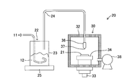
- FIG. 1 is a schematic diagram showing the configuration of a film forming apparatus used in the single crystal manufacturing method according to one embodiment of the present invention as described above.
- the film forming apparatus 20 includes an aerosol generating unit 22 that generates an aerosol of a raw material powder containing a raw material component, and a film forming unit 30 that sprays the film forming powder onto the seed substrate 21 to form a film containing the raw material component. ing.
- the aerosol generating unit 22 contains the film forming powder 12 and receives the supply of the carrier gas 11 from a gas cylinder (not shown) to generate an aerosol, and supplies the generated aerosol to the film forming unit 30.
- a raw material supply pipe 24, an aerosol generation chamber 23, and a vibrator 25 for applying vibration to the aerosol therein at a frequency of 10 to 100 Hz are provided.
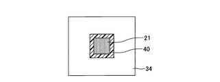
- the film forming unit 30 includes a film forming chamber 32 that injects aerosol onto the seed substrate 21, a seed substrate holder 34 that is disposed inside the film forming chamber 32 and fixes the seed substrate 21, and the seed substrate holder 34 is connected to the X axis ⁇ And an XY stage 33 that moves in the Y-axis direction.
- the film forming unit 30 includes a spray nozzle 36 that has a slit 37 formed at the tip thereof and sprays aerosol onto the seed substrate 21, and a vacuum pump 38 that decompresses the film forming chamber 32.
- nitrogen (N 2 ) gas is flowed as the carrier gas 11 at a flow rate of 6 L / min, the pressure in the aerosol generation chamber 23 is 50 to 70 kPa, and the pressure in the film forming chamber 32 is increased.
- the opening size of the slit 37 provided in the spray nozzle 36 for film forming powder was 10 mm ⁇ 0.8 mm.
- the opening size of the slit 37 was set to 10 mm ⁇ 0.4 mm.
- scanning was performed simultaneously with film formation at a scanning distance of 12 mm at the scanning speed and the number of scans listed in Table 1.
- the thickness of the various films thus obtained is such that a film forming part and a non-film forming part are formed on the substrate by masking a part of the substrate at the time of film formation.
- the thickness of the film was determined by measuring the level difference from the part.
- a small shape roughness measuring machine manufactured by Taylor-Hobson, “Form Talysurf plus” was used.
- the thicknesses of various films according to each experimental example are also listed in Table 1.
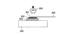
- FIG. 2 is a schematic diagram showing the configuration of the heating device used in the single crystal manufacturing method according to one embodiment of the present invention as described above.
- a near-infrared lamp 206 is used as a light source for light heating. Since the various films have a low near-infrared absorption coefficient, a platinum plate 203 is disposed on the surface opposite to the surface on which the film 201 of the seed substrate 202 is deposited, and the surface on which the film 201 of the seed substrate 202 is deposited.
- the film 201 was heated from the seed substrate 202 side by irradiating near infrared rays from the same side and causing the platinum plate 203 to absorb the near infrared rays.
- the seed substrate 202 and the platinum plate 203 were placed on a quartz pedestal 204, and the temperature of the film 201 was measured by a thermocouple 205.
- the heating temperature, the heating rate, and the holding time are as listed in Table 1.
- the film was heated from the seed substrate side by irradiating near infrared rays from the side opposite to the surface on which the film of the seed substrate 202 was deposited.
- an electric furnace was employed as the heating means, and the temperature of the entire heating chamber was heated by the electric furnace. In any sample, no change in the film thickness was observed before and after the heating step.
- a single crystal having a thickness of 250 ⁇ m in the direction perpendicular to the surface of the seed substrate was formed by repeating the film forming step and the heating step 100 times.
- In-plane rocking curve (XRC) measurement A multi-functional high-resolution X-ray diffractometer (Bulker AXS Co., Ltd., D8 DISCOVER) is used for the C-plane of various evaluation samples that have undergone the above heating step. In-plane rocking curve (XRC) measurements were made using under conditions. When the (100) peak was detected, it was judged that a dense single crystal film was obtained satisfactorily.
- Tube voltage 40kV ⁇ Tube current: 40 mA ⁇ Anti-scattering slit: 3 ° ⁇ Step width: 0.001 ° ⁇ Scanning speed: 0.5 seconds / step ⁇ Incident angle: 1 °
- ⁇ represents resistivity [ ⁇ ⁇ cm]
- F represents resistivity correction coefficient
- t represents film thickness [cm]
- R represents resistance [ ⁇ ].
- the resistivity correction coefficient F was calculated using the formula described in JIS K 7194.
- the thickness of the film deposited on the seed substrate exceeds 100 ⁇ m (Experimental Example 11), and the heating rate in the heating step is less than 30 ° C./min. (Experimental example 12)
- the entire film is heated gently and uniformly in the heating step (Experimental example 13)
- a large number of pores are generated in the film, and a dense single crystal film is obtained. It was confirmed that it was not possible. That is, when the requirements for the single crystal manufacturing method according to the present invention are not satisfied, it is difficult to obtain a good single crystal film.
- aluminum (Al) as an impurity was uniformly contained in the film in a concentration range of 0.1 to 0.3 at%. A single crystal having a very low resistivity of 10 ⁇ 3 ⁇ ⁇ cm or less could be obtained.
- the thickness of the film deposited on the seed substrate is 100 ⁇ m or less
- the heating rate in the heating step is 30 ° C./min or more
- the film is heated from the seed substrate side in the heating step.
- the present invention is such that the thickness of the film deposited on the seed substrate is 30 ⁇ m or less, the heating rate in the heating step is 300 ° C./min or more, and the film is heated from the seed substrate side in the heating step.
- the more preferable requirements of the single crystal manufacturing method according to the above are satisfied, it has extremely good quality from the viewpoints of pore suppression in the film, promotion of single crystallization, and homogeneous distribution of impurities (dopants) Single crystal films could be obtained (see, for example, Experimental Examples 01 to 04 and Experimental Examples 08 to 10).
- the amorphous film is formed in the film forming step, thereby facilitating the single crystallization in the heating step, so that the raw material melt can be easily obtained as well as the raw material melt. This was carried out for the purpose of verifying that it is possible to produce a high-quality single crystal with few pores with higher productivity even in a material system that is difficult to obtain.
- sample for evaluation Film formation step Using a RF magnetron sputtering apparatus, on a titanium oxide (TiO 2 ) single crystal substrate (rutile, 10 mm ⁇ 10 mm square, 0.5 mm thickness, (100) plane), An amorphous layer of titanium oxide (TiO 2 ) having a thickness of 1.5 ⁇ m was formed. In the film formation, a commercially available titanium oxide (TiO 2 ) sintered body target was used. The film forming conditions were a pure Ar atmosphere, a pressure of 1 Pa, a room temperature, an input power of 120 W, and a film forming time of 120 minutes.
- the amorphous film was heated using the heating apparatus shown in FIG. More specifically, the amorphous film was heated from the seed substrate side by irradiating near infrared rays from the side opposite to the surface on which the film of the seed substrate 202 was deposited.
- the heating conditions were a heating temperature of 1000 ° C., a heating rate of 400 ° C./min, and a holding time of 10 minutes in a pure Ar atmosphere. Also in the sample according to this example, no change in film thickness was observed before and after the heating step.
- zinc oxide (ZnO) doped with aluminum (Al) is formed on the surface of a seed substrate in which a single crystal of zinc oxide (ZnO) is formed on a sapphire (Al 2 O 3 ) substrate. This was carried out for the purpose of verifying that a single crystal having higher crystallinity can be obtained by producing a crystal layer as compared with the case where sapphire is used as a seed substrate.
- the support substrate is heated to 700 ° C. using a resistance heater, and the zinc oxide having a thickness of 100 nm is controlled while controlling the flux of the gas source so that the stoichiometric ratio of zinc (Zn) and oxygen (O) is reached.
- a single crystal layer of (ZnO) was formed as a seed substrate.
- Zinc oxide (ZnO) doped with aluminum (Al) by the same procedure as in Experimental example 10 of Example 1 except that the seed substrate prepared in (1) above was used.
- Single crystal Specifically, in the film forming step, zinc oxide (ZnO) powder in which aluminum (Al) is dissolved is formed on the surface of the seed substrate by the AD method, and in the heating step, FIG. Using the heating apparatus shown, the film was heated under the same conditions as in Experimental Example 10 of Example 1 described in Table 1. Note that a single crystal film of zinc oxide (ZnO) doped with aluminum (Al) having a thickness of 2.4 ⁇ m was formed by one cycle of the film forming step and the heating step. By repeating this cycle 100 times, a single crystal of zinc oxide (ZnO) doped with aluminum (Al) having a thickness of 240 ⁇ m could be produced.
- Example 2 Evaluation Method of Sample for Evaluation
- the following evaluation method was used as in Example 1.
- (1) Cross-sectional SEM observation The cross section of the obtained single crystal was observed by SEM, and the presence or absence of pores in the cross section and the state of the interface between the single crystal and the seed substrate were evaluated.
- (2) In-plane rocking curve (XRC) measurement The (100) peak detected by in-plane rocking curve (XRC) measurement was evaluated.
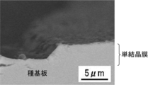
- Evaluation Results of Various Evaluation Samples 40 fields of view from the end of the film in the cross section were observed with a scanning electron microscope (SEM) at a magnification of 5000, but no pores were observed. Further, the interface between the film and the seed substrate disappeared.
- SEM scanning electron microscope
- a sharper (100) peak was detected as compared with Experimental Example 10 of Example 1. That is, in this example, it was possible to produce a single crystal having higher crystallinity as compared with Experimental Example 10 of Example 1.
- the heat treatment is performed in a state where warpage and / or undulation of the seed substrate is suppressed in the heating step, compared with the case where heat treatment is performed in a state where the warpage and / or undulation of the seed substrate is not suppressed, It carried out for the purpose of verifying that a single crystal having higher quality can be obtained.
- Example 41 and 44 those obtained by correcting the warpage and / or undulation of the seed substrate are referred to as “Experimental Examples 41 and 44”, respectively, and the warpage and / or undulation of the seed substrate is corrected. Those not present are simply referred to as “Experimental Examples 01 and 04”, respectively.
- Table 3 the seed substrates of Experimental Examples 41 and 44 in which the warpage and / or undulation of the seed substrate were corrected as described above showed warpage amounts of 2 ⁇ m and 5 ⁇ m, respectively. Furthermore, the quality (defect density) of the obtained single crystal was evaluated for each of the set of Experimental Example 01 and Experimental Example 41 and the set of Experimental Example 04 and Experimental Example 44.
- the cross section by the plane orthogonal to the main surface of a seed substrate is observed by TEM, and the defect density of the single crystal obtained in each sample Asked. More specifically, it includes an interface between at least the seed substrate and a portion where the film formed is single-crystallized (hereinafter sometimes referred to as “single-crystallized portion”) from each evaluation sample that has undergone the heating step.
- a section was cut out and processed by ion milling so that the thickness (T) of the section near the interface was 150 nm. The periphery of the interface of the section thus processed was observed with a TEM at a magnification of 50000 times, and a bright field image was taken.
- a line segment having a length (L) of 5000 nm parallel to the interface between the single crystallized part and the seed substrate is separated from the interface by 400 nm, 800 nm, 1200 nm, 1600 nm, and 2000 nm.
- a total of 5 lines were drawn at the locations, and the total number (S) of lattice defects present at positions overlapping these line segments was counted.
- a value (D) [/ cm 2 ] calculated based on the following formula (2) is calculated as the defect density (D) [/ cm 2 ] of the single crystal from the total number S of lattice defects thus obtained. did.
- the defect density (D) calculated for each sample for evaluation is also listed in Table 3.
- the amount of warpage in the seed substrate corresponding to Experimental Example 01 of Example 1 subjected to heat treatment in the heating step included in the single crystal manufacturing method according to the present invention is suppressed from 50 ⁇ m to 2 ⁇ m.
- the defect density in the resulting single crystal could be reduced from 5 ⁇ 10 8 pieces / cm 2 to 1 ⁇ 10 8 pieces / cm 2 .
- the amount of warpage in the seed substrate corresponding to Experimental Example 04 of Example 1 subjected to the heat treatment in the heating step included in the single crystal manufacturing method according to the present invention is suppressed as a result from 90 ⁇ m to 5 ⁇ m.
- the defect density in the obtained single crystal could be reduced from 7 ⁇ 10 8 pieces / cm 2 to 2 ⁇ 10 8 pieces / cm 2 .
Landscapes
- Chemical & Material Sciences (AREA)
- Engineering & Computer Science (AREA)
- Crystallography & Structural Chemistry (AREA)
- Materials Engineering (AREA)
- Metallurgy (AREA)
- Organic Chemistry (AREA)
- Physics & Mathematics (AREA)
- Thermal Sciences (AREA)
- Inorganic Chemistry (AREA)
- Manufacturing & Machinery (AREA)
- Crystals, And After-Treatments Of Crystals (AREA)
- Recrystallisation Techniques (AREA)
Abstract
先ずは所定値以下の厚みを有する膜を種基板上に成膜し、斯くして得られた膜を種基板側から所定値以上の昇温速度にて加熱することにより、単結晶を作製する。具体的には、例えば、種基板の表面上に膜を形成する成膜ステップにおいて、前記種基板の表面に直交する方向における厚みである膜厚が100μm以下である前記膜を形成し、次いで、前記種基板の表面上に形成された前記膜を加熱して単結晶を得る加熱ステップにおいて、前記膜を前記種基板の側から加熱して、30℃/分以上の昇温速度にて昇温させる。これにより、原料融液を得ることが容易な材料系のみならず、原料融液を得ることが困難な材料系においても気孔が少ない高品質な単結晶を作製可能な生産性に優れた単結晶製造方法を提供する。
Description
本発明は、単結晶製造方法に関する。より具体的には、本発明は、気孔が少なく均質な単結晶を高い生産性にて製造することができる単結晶製造方法に関する。更に、本発明は、当該方法によって製造される単結晶にも関する。
例えば、圧電ポンプ、インクジェットプリンタのインクヘッド等の種々の用途において使用される圧電アクチュエータに用いられる圧電体材料や、例えば、発光ダイオード(LED)、レーザーダイオード(LD)等の種々の半導体素子に用いられる半導体材料として、セラミックスを始めとする種々の無機材料が利用されている。かかる無機材料の性能を向上させるためには、これらの無機材料における結晶配向度を高くすることが重要であることが知られている。
例えば、圧電セラミックスにおいて、より高い圧電効果を発揮させるためには、圧電セラミックスに電界を印加することによって結晶中の電気双極子の向きを揃える処理(分極処理)が施されるが、この際、結晶配向度が高い程、より分極され易くなり、その結果、高い圧電性能を得ることができる。
ところで、単結晶膜や、結晶がある程度配向されている多結晶膜を含む配向膜(以降、「配向性多結晶膜」と称する場合がある)を形成する方法として、作製しようとする単結晶や配向性多結晶膜の原料融液を調製し、種となる単結晶上で結晶化させる方法がある。しかしながら、かかる方法において使用される酸化物(例えば、酸化亜鉛(ZnO)等)や窒化物(例えば、窒化ガリウム(GaN)等)や炭化物(例えば、炭化珪素(SiC)等)等の原料が非常に高い融点を有したり、もしくは分解し易かったりする場合がある。このような原料については原料融液を得ることが困難であり、かかる材料系に上記方法を適用することは困難であった。そこで、例えば、GaNの単結晶を作製しようとする場合において、ナトリウム(Na)をフラックスとして原料を溶解し、種に析出させて単結晶を得るNaフラックス法が提案されている(例えば、特許文献1を参照)。また、サファイア等の異種基板上にハイドライド気相成長法(Hydride Vapor Phase Epitaxy)を用いてGaN層を形成し、GaN層の成長後に異種基板を除去することにより、自立したGaNの単結晶基板を得る方法が提案されている(例えば、特許文献2を参照)。しかしながら、これらの従来技術に係る方法は、結晶の成長速度が遅いという問題を有する。
一方、固相成長法によって単結晶膜及び配向性多結晶膜を製造することもできる(例えば、特許文献3を参照)。具体的には、例えば、ペロブスカイト構造を有する酸化物からなり0.01~8体積%の気孔率を有する単結晶又は配向性多結晶が圧電材料等として優れた特性を発揮することができることが開示されている。また、特定の組成を有する酸化物粉末の成形体又は焼結体を所定の温度において熱処理することにより、配向性多結晶又は単位面積当たりに所定個数の小傾角粒界を形成する結晶粒子を含む単結晶から実質的に構成される良質な酸化物イオン伝導性結晶体を効率的に製造することが開示されている(例えば、特許文献4を参照)。
加えて、上記特許文献3及び4においては、結晶体を製造する1つの方法として、焼結体と単結晶(種基板)とを接触させた状態で、接触部分を加熱すると共にそれ以外の末端部分を冷却する温度制御を行うことにより所定の温度勾配を生じさせて、種基板を起点として多結晶の焼結体を単結晶化又は配向化することが開示されている(例えば、特許文献3の図4、特許文献4の図4を参照)。
しかしながら、かかる固相成長による結晶の配向化においては、以下に示すような問題が懸念される。先ず、上記のように焼結体と種基板とを接触させて接触部分を加熱することにより焼結体の微粒子を種基板の単結晶に取り込ませて固相成長させるためには、例えば、種基板の表面を鏡面研磨したり、焼結体と種基板とを加圧接触したり、両者の界面に空隙が生じないように、界面に液相材料を充填したりして、両者を密着させることが重要である。そのため、製造工程及び製造装置が複雑になる。特に、大面積の焼結体と種基板とを均一に密着させることは極めて困難である。
また、上記従来技術においては、多結晶の焼結体と種基板との接触部分を加熱すると共に当該焼結体の他の末端領域を冷却することにより所定の温度勾配を生じさせているが、温度勾配が小さい場合は、焼結体と種基板との界面では固相成長するものの、当該界面から離れた焼結体の内部では個々の粒子において別個に粒成長が進む。この結果、固相成長が進むにつれて種結晶に取り込まれる粒子が粗大となり、最終的には固相成長が停止する。また、粗大粒子が別個に種結晶に取り込まれるため、膜中に気孔が残留しやすい。一方、このような問題を防ぐために温度勾配を過大にするとワークそのものが破損する虞がある。
そこで、当該技術分野においては、原料の粉体(原料粉)の粒径が種基板から離れるに従って次第に大きくなるようにエアロゾルデポジション法(以降、「AD法」と称する場合がある)によって粒径の異なる原料粉を種基板上に噴射し、種基板上に堆積させ、斯くして形成された原料を含む膜を熱処理することにより、良質な単結晶膜又は配向性多結晶膜を製造する技術が開示されている(例えば、特許文献5を参照)。
しかしながら、上記従来技術に係る単結晶膜及び配向性多結晶膜の製造方法は、上記のように非常に複雑であり、且つ手間がかかる。また、固相成長の進行方向を制御して結晶粒の配向を制御するために原料粉に混入される固溶不純物及び配向化温度をより低温側にシフトさせるために原料粉の膜に添加される焼結助剤の膜内での濃度分布を狙い通りに正確に制御することは極めて困難であり、均質な結晶を得ることが難しい。また、上述した特許文献3及び4に記載の方法と同様に、膜と種基板との界面から離れた領域に存在する粒子は熱処理によって粒成長して粗大粒子となるため、固相成長には多大なエネルギーが必要となり、最終的には固相成長が停止する。また、粗大粒子が別個に取り込まれるため、膜中に気孔が残留しやすい。
以上のように、当該技術分野においては、原料融液を得ることが容易な材料系のみならず、原料融液を得ることが困難な材料系においても気孔が少ない高品質な単結晶を作製可能な生産性に優れた単結晶製造方法に対する要求が存在する。
上述のように、当該技術分野においては、原料融液を得ることが容易な材料系のみならず、原料融液を得ることが困難な材料系においても気孔が少ない高品質な単結晶を作製可能な生産性に優れた単結晶製造方法に対する要求が存在する。本発明は、かかる要求に応えるために為されたものである。即ち、本発明は、原料融液を得ることが容易な材料系のみならず、原料融液を得ることが困難な材料系においても気孔が少ない高品質な単結晶を作製可能な生産性に優れた単結晶製造方法を提供することを1つの目的とする。
本発明の上記1つの目的は、
種基板の表面上に膜を形成する成膜ステップ、及び
前記種基板の表面上に形成された前記膜を加熱して単結晶を得る加熱ステップ、
を含む単結晶製造方法であって、
前記成膜ステップにおいて形成される前記膜の前記種基板の表面に直交する方向における厚みである膜厚が100μm以下であること、
前記加熱ステップにおいて前記膜が前記種基板の側から加熱されること、及び
前記加熱ステップにおける前記膜の昇温速度が30℃/分以上であること、
を特徴とする単結晶製造方法によって達成される。
種基板の表面上に膜を形成する成膜ステップ、及び
前記種基板の表面上に形成された前記膜を加熱して単結晶を得る加熱ステップ、
を含む単結晶製造方法であって、
前記成膜ステップにおいて形成される前記膜の前記種基板の表面に直交する方向における厚みである膜厚が100μm以下であること、
前記加熱ステップにおいて前記膜が前記種基板の側から加熱されること、及び
前記加熱ステップにおける前記膜の昇温速度が30℃/分以上であること、
を特徴とする単結晶製造方法によって達成される。
本発明に係る単結晶製造方法によれば、原料融液を得ることが容易な材料系のみならず、原料融液を得ることが困難な材料系においても、気孔が少ない高品質な単結晶を高い生産性にて作製することができる。
前述のように、当該技術分野においては、原料融液を得ることが容易な材料系のみならず、原料融液を得ることが困難な材料系においても気孔が少ない高品質な単結晶を作製可能な生産性に優れた単結晶製造方法に対する要求が存在する。本発明は、かかる要求に応えるために為されたものである。即ち、本発明は、原料融液を得ることが容易な材料系のみならず、原料融液を得ることが困難な材料系においても気孔が少ない高品質な単結晶を作製可能な生産性に優れた単結晶製造方法を提供することを1つの目的とする。
本発明者は、上記目的を達成すべく鋭意研究の結果、先ずは所定値以下の厚みを有する膜を種基板上に成膜し、斯くして得られた膜を種基板側から所定値以上の昇温速度にて加熱することにより、原料融液を得ることが容易な材料系のみならず、原料融液を得ることが困難な材料系においても、気孔が少ない高品質な単結晶を高い生産性にて作製することができることを見出し、本発明を想到するに至ったものである。
即ち、本発明の第1の実施態様は、
種基板の表面上に膜を形成する成膜ステップ、及び
前記種基板の表面上に形成された前記膜を加熱して単結晶を得る加熱ステップ、
を含む単結晶製造方法であって、
前記成膜ステップにおいて形成される前記膜の前記種基板の表面に直交する方向における厚みである膜厚が100μm以下であること、
前記加熱ステップにおいて前記膜が前記種基板の側から加熱されること、及び
前記加熱ステップにおける前記膜の昇温速度が30℃/分以上であること、
を特徴とする単結晶製造方法である。
種基板の表面上に膜を形成する成膜ステップ、及び
前記種基板の表面上に形成された前記膜を加熱して単結晶を得る加熱ステップ、
を含む単結晶製造方法であって、
前記成膜ステップにおいて形成される前記膜の前記種基板の表面に直交する方向における厚みである膜厚が100μm以下であること、
前記加熱ステップにおいて前記膜が前記種基板の側から加熱されること、及び
前記加熱ステップにおける前記膜の昇温速度が30℃/分以上であること、
を特徴とする単結晶製造方法である。
上記のように、本実施態様に係る単結晶製造方法は、種基板の表面上に膜を形成する成膜ステップ、及び前記種基板の表面上に形成された前記膜を加熱して単結晶を得る加熱ステップ、を含む単結晶製造方法である。一方、当該技術分野においても、前述のように、例えば、AD法によって原料粉を噴射して種基板上に堆積させ(本実施態様に係る単結晶製造方法における成膜ステップに対応)、斯くして形成された原料を含む膜を熱処理する(本実施態様に係る単結晶製造方法における加熱ステップに対応)ことにより、単結晶膜を製造することが既に提案されている(例えば、特許文献5を参照)。しかしながら、前述のように、上記を始めとする従来技術に係る単結晶製造方法は、工程が複雑であったり、均質な結晶を得ることが困難であったり、気孔の発生を抑えることが困難であったりして、気孔が少ない高品質な単結晶を高い生産性にて作製することが難しいのが実情であった。
しかしながら、本実施態様に係る単結晶製造方法においては、先ずは所定値以下の厚みを有する膜を種基板上に成膜し、斯くして得られた膜を種基板側から所定値以上の昇温速度にて加熱する。具体的には、本実施態様に係る単結晶製造方法においては、上述のように、先ず成膜ステップにおいて、種基板の表面に直交する方向における厚みである膜厚が100μm以下である膜を種基板の表面上に形成し、次に加熱ステップにおいて、種基板の表面上に形成された膜を種基板の側から加熱して、30℃/分以上の昇温速度にて膜を昇温させる。これにより、本実施態様に係る単結晶製造方法においては、原料融液を得ることが容易な材料系のみならず、原料融液を得ることが困難な材料系においても、気孔が少ない高品質な単結晶を高い生産性にて作製することができる。尚、本実施態様に係る単結晶製造方法によって単結晶を得る物質の主成分は、特に限定されないが、例えば、種々のセラミックス、酸化亜鉛(ZnO)、酸化チタン(TiO2)等の酸化物、及び窒化ガリウム(GaN)等の窒化物等を挙げることができる(詳しくは後述する)。
ところで、上記のように所定値以下の厚みを有する膜を所定値以上の昇温速度にて加熱することにより気孔が少ない高品質な単結晶が得られる詳細なメカニズムについては未だ解明されていない。しかしながら、上記のように所定値以下の厚みを有する膜を所定値以上の昇温速度にて加熱することにより、膜内に適度な温度勾配が生じ、膜内の粒成長を抑えつつ膜と種基板との界面から固相成長が順次進むため、気孔の発生が抑制されたものと考えられる。
尚、本実施態様に係る単結晶製造方法に含まれる成膜ステップにおいて種基板の表面上に形成される膜の(種基板の表面に直交する方向における厚みである)膜厚は100μm以下であることが望ましく、より好ましくは30μm以下であることが望ましい。また、本実施態様に係る単結晶製造方法に含まれる加熱ステップにおける膜の昇温速度は30℃/分以上であることが望ましく、より好ましくは300℃/分以上であることが望ましい。
従って、本発明の第2の実施態様は、
本発明の前記第1の実施態様に係る単結晶製造方法であって、
前記成膜ステップにおいて形成される前記膜の膜厚が30μm以下であること、
を特徴とする単結晶製造方法である。
本発明の前記第1の実施態様に係る単結晶製造方法であって、
前記成膜ステップにおいて形成される前記膜の膜厚が30μm以下であること、
を特徴とする単結晶製造方法である。
また、本発明の第3の実施態様は、
本発明の前記第1又は前記第2の実施態様の何れか1つに係る単結晶製造方法であって、
前記加熱ステップにおける前記膜の昇温速度が300℃/分以上であること、
を特徴とする単結晶製造方法である。
本発明の前記第1又は前記第2の実施態様の何れか1つに係る単結晶製造方法であって、
前記加熱ステップにおける前記膜の昇温速度が300℃/分以上であること、
を特徴とする単結晶製造方法である。
更に、本発明に係る単結晶製造方法に含まれる成膜ステップにおいて種基板の表面上に膜を形成する方法は、種基板との良好な密着性を有し且つ膜内に(ミクロンオーダー(即ち大きさが1μm以上)の)気孔が生じない緻密な膜を種基板上に形成することが可能である限り、特に限定されるものではない。具体的には、本発明に係る単結晶製造方法に含まれる成膜ステップにおいては、例えば、対象となる基板等に向けて粉末を噴射して当該基板上に当該粉体を固化させることにより成膜する粉末法、膜の主成分及び/又は先駆物質を含んでなる溶液を用いて当該主成分及び/又は先駆物質を基板等の表面に析出若しくは被覆させることにより成膜する溶液法、物理蒸着(PVD)法、及び化学蒸着(CVD)法からなる群より選ばれる何れの方法によって、種基板の表面上に膜を形成してもよい。上記粉末法の具体例としては、例えば、エアロゾルデポジション法(AD法)及びパウダージェットデポジション法(PJD法)等を挙げることができる。また、上記溶液法の具体例としては、例えば、液相析出法、スピンコーティング法、及びディッピング法等を挙げることができる。更に、上記物理蒸着(PVD)法の具体例としては、例えば、スパッタ法等を挙げることができる。また更に、化学蒸着(CVD)法としては、例えば、ミストCVD法及びレーザーCVD法等を挙げることができる。
従って、本発明の第4の実施態様は、
本発明の前記第1乃至前記前記第3の実施態様の何れか1つに係る単結晶製造方法であって、
前記成膜ステップにおいて前記種基板の表面上に前記膜を形成する方法が、粉末法、溶液法、物理蒸着(PVD)法、及び化学蒸着(CVD)法からなる群より選ばれる何れかの方法であること、
を特徴とする単結晶製造方法である。
本発明の前記第1乃至前記前記第3の実施態様の何れか1つに係る単結晶製造方法であって、
前記成膜ステップにおいて前記種基板の表面上に前記膜を形成する方法が、粉末法、溶液法、物理蒸着(PVD)法、及び化学蒸着(CVD)法からなる群より選ばれる何れかの方法であること、
を特徴とする単結晶製造方法である。
また、本発明の第5の実施態様は、
本発明の前記第4の実施態様に係る単結晶製造方法であって、
前記粉末法がエアロゾルデポジション法(AD法)及びパウダージェットデポジション法(PJD法)からなる群より選ばれる何れかの方法であり、前記溶液法が、液相析出法、スピンコーティング法、及びディッピング法からなる群より選ばれる何れかの方法であり、前記物理蒸着(PVD)法がスパッタ法であり、前記化学蒸着(CVD)法がミストCVD法及びレーザーCVD法からなる群より選ばれる何れかの方法であること、
を特徴とする単結晶製造方法である。
本発明の前記第4の実施態様に係る単結晶製造方法であって、
前記粉末法がエアロゾルデポジション法(AD法)及びパウダージェットデポジション法(PJD法)からなる群より選ばれる何れかの方法であり、前記溶液法が、液相析出法、スピンコーティング法、及びディッピング法からなる群より選ばれる何れかの方法であり、前記物理蒸着(PVD)法がスパッタ法であり、前記化学蒸着(CVD)法がミストCVD法及びレーザーCVD法からなる群より選ばれる何れかの方法であること、
を特徴とする単結晶製造方法である。
上記実施態様に係る単結晶製造方法においては、前記成膜ステップにおいて前記種基板の表面上に前記膜を形成する方法として、粉末法、溶液法、物理蒸着(PVD)法、及び化学蒸着(CVD)法からなる群より選ばれる何れかの方法が採用される。その結果、本実施態様に係る単結晶製造方法によれば、種基板との良好な密着性を有し且つ膜内に(ミクロンオーダー(即ち大きさが1μm以上)の)気孔が生じない緻密な膜を種基板上に確実に形成することができる。より好ましくは、前記粉末法がエアロゾルデポジション法(AD法)及びパウダージェットデポジション法(PJD法)からなる群より選ばれる何れかの方法であり、前記溶液法が、液相析出法、スピンコーティング法、及びディッピング法からなる群より選ばれる何れかの方法であり、前記物理蒸着(PVD)法がスパッタ法であり、前記化学蒸着(CVD)法がミストCVD法及びレーザーCVD法からなる群より選ばれる何れかの方法である。尚、上記成膜方法の各々の詳細については当業者に周知であるので、本明細書においては説明を省略する。
前記粉末法としてエアロゾルデポジション法(AD法)又はパウダージェットデポジション法(PJD法)を用いる場合、膜側に圧縮応力、種基板側に引張応力が加わることが知られており、表面上に前記膜が形成(成膜)された種基板に反り及び/又はうねりが生ずる場合がある。かかる状態のままで熱処理(本発明に係る単結晶製造方法における加熱ステップに対応)を行うと、得られた単結晶中に転位等の格子欠陥が発生し易く、得られる単結晶の品質が低下する虞がある。このため、エアロゾルデポジション法(AD法)又はパウダージェットデポジション法(PJD法)を用いて成膜された種基板に限らず、反り及び/又はうねりが生じている種基板を熱処理する場合は、例えば金属製又はセラミックス製の治具を用いる等して、種基板の反り及び/又はうねりを矯正した状態で熱処理を行う方が望ましい。尚、種基板の反り及び/又はうねりを矯正するための手法は、上記のように金属製又はセラミックス製の治具を用いる手法に限定されるものではなく、例えば、真空チャック、静電チャック等を用いる手法を採用してもよい。
例えば、後述する実施例1の実験例1~10においては、成膜後の種基板202に反りが生じ、種基板202の中央部が台座から5~50μm程度、あるいはそれ以上、浮き上がっていたことが確認された。このとき種基板202の表面粗さ測定を行ったところ、断面曲線最大高さ(Pt)も5~50μm程度、あるいはそれ以上になっていたことが確認された。このように種基板に反りが生じていると、次の加熱ステップにおける熱処理が不十分及び/又は不均一となったり、上述したように単結晶中に転位等の格子欠陥が発生し易くなり、結果として得られる単結晶の品質が低下したりする虞がある。そこで、石英製の治具を用いて種基板202を白金板203及び石英製の台座204に固定し、反り量を5μm以下に矯正した状態で加熱ステップにおける熱処理を行ったところ、このように反りを矯正しない状態のままで熱処理を行った場合と比較して、単結晶中の欠陥が低減し、結晶性が向上した。尚、得られた単結晶にアニール処理を施して、単結晶中の転位等の格子欠陥を低減してもよい。例えば、酸化亜鉛(ZnO)単結晶の場合、大気中で300~900℃程度の温度範囲においてアニール処理を実施してもよい。また、酸化亜鉛(ZnO)単結晶の場合、高温においてアニール処理を実施すると酸素欠損が生じたり、酸化亜鉛(ZnO)自身が昇華したりする可能性がある。かかる場合においては、酸化亜鉛(ZnO)粉末等をアニール雰囲気中に共存させて、酸化亜鉛(ZnO)蒸気が存在する雰囲気中でアニール処理を実施してもよい。
尚、種基板の反り及び/又はうねりは、上記のように本発明に係る単結晶製造方法に含まれる加熱ステップにおける結晶成長に悪影響を及ぼすばかりでなく、成膜ステップにおいてエアロゾルデポジション法(AD法)又はパウダージェットデポジション法(PJD法)を用いて種基板の表面上に形成される膜の品質及び厚みにも悪影響を及ぼす場合がある。具体的には、成膜ステップにおいてエアロゾルデポジション法(AD法)又はパウダージェットデポジション法(PJD法)を用いて表面上に膜を形成しようとする種基板に反り及び/又はうねりがあると、種基板の表面に向かって噴射された粉末(粒子)が種基板の表面に衝突する角度が場所によって変化する。その結果、種基板の表面に形成される膜の品質及び/又は厚みが不均質となる虞がある。特に、大面積の種基板を使用する場合は、成膜に伴う種基板の反り及び/又はうねりが大きくなるため、均質な成膜を行うことがより困難となる。また、種基板の反り及び/又はうねりが生じている場合は、種基板の表面に向かって噴射された粉末が種基板の表面に衝突する際に反りやうねりの部分が変形して、衝突の衝撃を緩和してしまう。その結果、膜の形成に必要なエネルギーを確保することが困難となり、結果として種基板の表面に形成される膜の品質及び/又は厚みが不均質となる虞がある。かかる膜の品質及び/又は厚みの不均質さが次の加熱ステップにおける熱処理後に得られる単結晶の品質の均質性に影響することは言うまでもない。
上記のように、種基板の反り及び/又はうねりは、本発明に係る単結晶製造方法に含まれる加熱ステップにおける結晶成長のみならず、エアロゾルデポジション法(AD法)又はパウダージェットデポジション法(PJD法)を用いる成膜プロセスによって形成される膜の品質及び厚みの均質性にも悪影響を及ぼす場合がある。従って、本発明に係る単結晶製造方法に限らず、成膜ステップにおいてエアロゾルデポジション法(AD法)又はパウダージェットデポジション法(PJD法)を用いて膜を形成しようとする場合は、例えば、金属製又はセラミックス製の治具、あるいは真空チャック又は静電チャック等を用いて、反り及び/又はうねりを矯正した状態で種基板を台座に固定し、種基板に反り及び/又はうねりが存在しない状態で成膜を行うことが望ましい。
ところで、本発明に係る単結晶製造方法に含まれる加熱ステップにおいて膜を加熱する方法は、上述した昇温速度を実現可能である限り、特に限定されるものではない。かかる観点からは、例えば、赤外線ランプ(例えば、近赤外線ランプ等)、各種レーザー(例えば、CO2レーザー、YAGレーザー、エキシマーレーザー、半導体レーザー等)等を熱源とする光加熱や高周波加熱装置等が望ましい。
従って、本発明の第6の実施態様は、
本発明の前記第1乃至前記第5の実施態様の何れか1つに係る単結晶製造方法であって、
前記加熱ステップにおいて前記種基板の表面上に形成された前記膜を加熱する方法が、赤外線ランプ、レーザー、及び高周波加熱装置からなる群より選ばれる何れかの熱源を使用する加熱方法であること、
を特徴とする単結晶製造方法である。
本発明の前記第1乃至前記第5の実施態様の何れか1つに係る単結晶製造方法であって、
前記加熱ステップにおいて前記種基板の表面上に形成された前記膜を加熱する方法が、赤外線ランプ、レーザー、及び高周波加熱装置からなる群より選ばれる何れかの熱源を使用する加熱方法であること、
を特徴とする単結晶製造方法である。
上記のように、本実施態様に係る単結晶製造方法においては、前記加熱ステップにおいて前記種基板の表面上に形成された前記膜を加熱する方法が、赤外線ランプ、レーザー、及び高周波加熱装置からなる群より選ばれる何れかの熱源を使用する加熱方法である。これにより、本実施態様に係る単結晶製造方法においては、加熱ステップにおける膜の昇温速度を、確実且つ容易に30℃/分以上、より好ましくは300℃/分以上とすることができる。その結果、本実施態様に係る単結晶製造方法によれば、加熱ステップにおいて単結晶を得る過程における気孔の発生をより確実且つ容易に抑制することができる。
ところで、加熱ステップにおいて種基板の表面上に形成された膜を加熱する際には、加熱により膜中での物質移動が生じることにより、単結晶化が起こると考えられる。従って、単結晶化前の膜の状態としては、結晶性が低い状態にある方が、既存の結晶格子による拘束が少ないことに加えて、結晶化エネルギーを駆動力とすることができるため、単結晶化が進行し易いと考えられる。かかる観点から、本発明に係る単結晶製造方法においては、種基板の表面上に形成される膜は、結晶性が低い膜(以降、「微結晶膜」と称する場合がある)であることがより望ましく、非晶質膜であることがより一層望ましい。
従って、本発明の第7の実施態様は、
本発明の前記第1乃至前記第6の実施態様の何れか1つに係る単結晶製造方法であって、
前記成膜ステップにおいて形成される前記膜が非晶質であること、
を特徴とする単結晶製造方法である。
本発明の前記第1乃至前記第6の実施態様の何れか1つに係る単結晶製造方法であって、
前記成膜ステップにおいて形成される前記膜が非晶質であること、
を特徴とする単結晶製造方法である。
上記実施態様に係る単結晶製造方法においては、前記成膜ステップにおいて形成される前記膜が非晶質である。これにより、本実施態様に係る単結晶製造方法においては、上述したように単結晶化が進行し易くなり、原料融液を得ることが容易な材料系のみならず、原料融液を得ることが困難な材料系においても気孔が少ない高品質な単結晶をより高い生産性にて作製することが可能となる。
尚、本発明に係る単結晶製造方法に含まれる成膜ステップにおいて種基板の表面上に形成される膜の結晶性は、例えば、当該膜のXRD測定を行い、WPPD法によって結晶子サイズを算出することによって評価することができる。例えば、後述する実施例1の実験例01における成膜ステップ後の膜につき、封入管式X線回折装置(ブルカー・エイエックスエス製、D8 ADVANCE)を下記条件にて使用して測定した結晶子サイズは10.85nmであった。
・管電圧:40kV
・管電流:40mA
・ステップ幅:0.02°
・測定範囲:2θ=20~70°
・結晶子サイズの計算:WPPD法
・管電圧:40kV
・管電流:40mA
・ステップ幅:0.02°
・測定範囲:2θ=20~70°
・結晶子サイズの計算:WPPD法
本明細書においては、上記WPPD法によって算出される結晶子サイズが50nmを超えるものを多結晶膜とし、50nm以下となるものを微結晶膜とする。また、「非晶質」とは、面内ロッキングカーブ(XRC)測定において結晶に起因する回折ピークが現れない性状を指すものとする。
上記実施態様に係る単結晶製造方法に含まれる成膜ステップにおいて種基板の表面上に非晶質膜を形成する方法は、上述したように、種基板との良好な密着性を有し且つ膜内に(ミクロンオーダー(即ち大きさが1μm以上)の)気孔が生じない緻密な膜を種基板上に形成することが可能である限り、特に限定されるものではない。具体的には、本実施態様に係る単結晶製造方法に含まれる成膜ステップにおいて非晶質膜を形成する場合においても、例えば、対象となる基板等に向けて粉末を噴射して当該基板上に当該粉体を固化させることにより成膜する粉末法、膜の主成分及び/又は先駆物質を含んでなる溶液を用いて当該主成分及び/又は先駆物質を基板等の表面に析出若しくは被覆させることにより成膜する溶液法、物理蒸着(PVD)法、及び化学蒸着(CVD)法からなる群より選ばれる何れの方法によって、種基板の表面上に非晶質膜を形成することができる。上述したように、上記粉末法の具体例としては、例えば、エアロゾルデポジション法(AD法)及びパウダージェットデポジション法(PJD法)等を挙げることができる。また、上記溶液法の具体例としては、例えば、液相析出法、スピンコーティング法、及びディッピング法等を挙げることができる。更に、上記物理蒸着(PVD)法の具体例としては、例えば、スパッタ法等を挙げることができる。また更に、化学蒸着(CVD)法としては、例えば、ミストCVD法及びレーザーCVD法等を挙げることができる。
ところで、本発明に係る単結晶製造方法に含まれる成膜ステップにおいて種基板の表面上に形成される膜の主成分は、目的とする単結晶を作製することが可能である限り、特に限定されない。一般に酸化物又は窒化物(例えば、酸化亜鉛(ZnO)、酸化チタン(TiO2)、窒化ガリウム(GaN)等)を主成分とする単結晶を作製しようとする場合、加熱ステップにおいて過剰な熱エネルギーが与えられると、これらの材料の分解や昇華により、得られる結晶膜に組成ずれ及び気孔が発生し易くなる。一方、本発明に係る単結晶製造方法は、上述のように所定値以下の厚みを有する膜を所定値以上の昇温速度にて加熱することにより、膜内に適度な温度勾配が生じ、得られる結晶膜における気孔の発生を抑制することができる。即ち、本発明に係る単結晶製造方法は、酸化物又は窒化物を主成分とする単結晶を得ようとする場合に、特に好適に適用することができる。
また、本発明に係る単結晶製造方法に含まれる成膜ステップにおいて種基板の表面上に形成される膜の主成分と本発明に係る単結晶製造方法によって作製される単結晶の主成分とは、同じであっても、あるいは異なっていてもよい。例えば、上述したように成膜ステップにおいて形成される膜を非晶質としようとする際に、例えば、目的とする単結晶の主成分と同じ物質を主成分として含有する膜を(例えば、上述した各種方法の何れかによって)形成させると、形成される膜が結晶化してしまう場合がある。かかる場合には、成膜ステップにおいては最終的な単結晶とは異なる組成を有する先駆物質によって膜を形成させ、後の加熱ステップにおいて当該先駆物質を単結晶の主成分へと化学変化させて単結晶化させることにより、目的とする単結晶を得ることができる。かかる先駆物質の具体例としては、例えば、酸窒化亜鉛(ZnON)を挙げることができる。酸化亜鉛(ZnO)はスパッタ法によって成膜すると結晶化してしまう。しかしながら、スパッタ法による成膜時に窒素を導入することにより、酸化亜鉛(ZnO)の結晶核の発生が抑制され、結晶核密度の低い酸窒化亜鉛(ZnON)膜が得られる(例えば、特許文献6を参照)。その後、加熱ステップにおける熱処理により、目的とする酸化亜鉛(ZnO)の単結晶を得ることができる。
従って、本発明の第8の実施態様は、
本発明の前記第1乃至前記第7の実施態様の何れか1つに係る単結晶製造方法であって、
前記膜の主成分が、酸化物及び窒化物、並びにそれらの先駆物質からなる群より選ばれる何れか1種の材料であること、
を特徴とする単結晶製造方法である。
本発明の前記第1乃至前記第7の実施態様の何れか1つに係る単結晶製造方法であって、
前記膜の主成分が、酸化物及び窒化物、並びにそれらの先駆物質からなる群より選ばれる何れか1種の材料であること、
を特徴とする単結晶製造方法である。
尚、本実施態様に係る単結晶製造方法において種基板の表面上に形成される膜の主成分として使用することができる酸化物及び窒化物の具体例としては、上述のように、それぞれ酸化亜鉛(ZnO)、酸化チタン(TiO2)、及び窒化ガリウム(GaN)を挙げることができる。
従って、本発明の第9の実施態様は、
本発明の前記第8の実施態様に係る単結晶製造方法であって、
前記酸化物が酸化亜鉛(ZnO)及び酸化チタン(TiO2)であり、前記窒化物が窒化ガリウム(GaN)であること、
を特徴とする単結晶製造方法である。
本発明の前記第8の実施態様に係る単結晶製造方法であって、
前記酸化物が酸化亜鉛(ZnO)及び酸化チタン(TiO2)であり、前記窒化物が窒化ガリウム(GaN)であること、
を特徴とする単結晶製造方法である。
尚、上記のように、例えば、酸化亜鉛(ZnO)、酸化チタン(TiO2)、及び窒化ガリウム(GaN)等の昇華性が高い材料を膜の主成分として使用する場合、かかる材料が加熱ステップにおいて昇華して、結果として得られる単結晶に組成ずれ又は気孔が発生する等の問題を招くことを抑制することが望ましい。かかる目的を達成するための方策としては、例えば、加熱ステップにおける最高到達温度に上限を設けたり、最高到達温度での保持時間に上限を設けたりすることが挙げられる。但し、この場合、膜の主成分として使用する物質の融点、膜の厚み等を十分に考慮して、これらの上限を定める必要がある。
ところで、本発明に係る単結晶製造方法において使用される種基板として、単結晶層が表面に成膜された基板を使用してもよい。当該単結晶層は、例えば薄膜製造法によって基板上に成膜してもよい。この場合、本発明に係る単結晶製造方法によって製造される単結晶の原料を含んでなる膜は、単結晶層の表面上に形成される。
従って、本発明の第10の実施態様は、
本発明の前記第1乃至前記第9の実施態様の何れか1つに係る単結晶製造方法であって、
前記種基板が、単結晶層が表面上に成膜された基板であること、及び
前記単結晶層の表面上に前記膜が形成されること、
を特徴とする単結晶製造方法である。
本発明の前記第1乃至前記第9の実施態様の何れか1つに係る単結晶製造方法であって、
前記種基板が、単結晶層が表面上に成膜された基板であること、及び
前記単結晶層の表面上に前記膜が形成されること、
を特徴とする単結晶製造方法である。
上記のように、本実施態様に係る単結晶製造方法においては、単結晶層が表面上に成膜された基板が種基板として使用され、本発明に係る単結晶製造方法によって製造される単結晶の原料を含んでなる膜は、当該単結晶層の表面上に形成される。基板は、単結晶層をその表面上に形成することが可能であり且つ本発明に係る単結晶製造方法において悪影響を及ぼさない限り特に限定されない。
また、種基板となる単結晶層を基板の表面上に成膜する方法も特に限定されないが、具体例としては、例えば、固相エピタキシャル成長法、気相エピタキシャル成長法、液相エピタキシャル法等を挙げることができる。気相エピタキシャル成長法の具体例としては、例えば、分子線エピタキシー(MBE)法、ラジカルソース分子線エピタキシー(RS-MBE)法、有機金属気相成長法(MOCVD)法、パルスレーザーデポジション(PLD)法、スパッタリング法等を挙げることができる。液相エピタキシャル成長法の具体例としては、例えば、液相析出法、フラックス法、水熱法、スピンコート法、ディッピング法等を挙げることができる。
かかる種基板を使用する本実施態様に係る単結晶製造方法の実施形態の一例としては、例えば、上記MBE法によりサファイアからなる基板の表面上に酸化亜鉛(ZnO)の単結晶層を成膜して得られる種基板を使用し、成膜ステップにおいて当該種基板の単結晶層の表面上にAD法により酸化亜鉛(ZnO)の原料粉を含んでなる膜を成膜し、加熱ステップにおいて所定の条件下にて当該膜を加熱することにより酸化亜鉛(ZnO)の単結晶を作製するプロセスを挙げることができる。この場合、サファイアからなる基板から見れば、上記実施形態に係る単結晶製造方法による酸化亜鉛(ZnO)の単結晶の作製はヘテロエピタキシャル成長に該当するが、上述したように、当該種基板においては酸化亜鉛(ZnO)の単結晶層がその表面上に成膜されている結果、ホモエピタキシャル成長となり、より良好な結晶性を有する酸化亜鉛(ZnO)の単結晶を得ることができる。
ところで、本発明に係る単結晶製造方法によれば、成膜ステップにおいて、当該方法によって製造しようとする単結晶の原料を含む膜が種基板の表面上に形成(成膜)され、加熱ステップにおいて、斯くして種基板の表面上に形成された膜が所定の条件下にて熱処理に付され、目的とする単結晶が得られる。前述したように、加熱ステップにおいて上記膜が熱処理に付される際に種基板に反り及び/又はうねりが存在すると、単結晶中に転位等の格子欠陥が発生し易く、結果として得られる単結晶の品質が低下する虞がある。従って、本発明に係る単結晶製造方法に含まれる加熱ステップにおいて上記膜を熱処理する際には、例えば金属製又はセラミックス製の治具を用いる等して、種基板の反り及び/又はうねりが抑制された状態で熱処理を行う方が望ましい。
即ち、本発明の第11の実施態様は、
本発明の前記第1乃至前記第10の実施態様の何れか1つに係る単結晶製造方法であって、
前記加熱ステップにおいて、前記種基板の反り及び/又はうねりに対応する評価指標が予め定められた上限値以下である状態で、前記膜を加熱すること、
を特徴とする単結晶製造方法である。
本発明の前記第1乃至前記第10の実施態様の何れか1つに係る単結晶製造方法であって、
前記加熱ステップにおいて、前記種基板の反り及び/又はうねりに対応する評価指標が予め定められた上限値以下である状態で、前記膜を加熱すること、
を特徴とする単結晶製造方法である。
上記のように、本実施態様に係る単結晶製造方法においては、前記加熱ステップにおいて、前記種基板の反り及び/又はうねりに対応する評価指標が予め定められた上限値以下である状態で、前記膜を加熱する。これにより、本実施態様に係る単結晶製造方法においては、単結晶中に転位等の格子欠陥が発生し難くなり、結果として得られる単結晶の品質が向上する。尚、種基板の反り及び/又はうねりに対応する評価指標は、例えば、本実施態様に係る単結晶製造方法によって製造される単結晶の用途において求められる品質を達成し得る種基板の反り及び/又はうねりの大きさ及び周期等に応じて適宜選択することができる。かかる評価指標としては、例えば、表面形状・粗さ測定機等によって測定される種々の表面性状パラメータ等を採用することができる。
また、かかる評価指標について予め定められた上限値もまた、例えば、本実施態様に係る単結晶製造方法によって製造される単結晶の用途において求められる品質を達成し得る種基板の反り及び/又はうねりの大きさ及び周期等に応じて適宜定めることができる。より具体的には、上記予め定められた上限値は、例えば、本実施態様に係る単結晶製造方法によって製造される単結晶の用途において許容可能な格子欠陥の存在頻度(以降、「欠陥密度」と称する場合がある)を与える種基板の反り及び/又はうねりに対応する上記評価指標の最大値として定義することができる。
また、かかる評価指標について予め定められた上限値もまた、例えば、本実施態様に係る単結晶製造方法によって製造される単結晶の用途において求められる品質を達成し得る種基板の反り及び/又はうねりの大きさ及び周期等に応じて適宜定めることができる。より具体的には、上記予め定められた上限値は、例えば、本実施態様に係る単結晶製造方法によって製造される単結晶の用途において許容可能な格子欠陥の存在頻度(以降、「欠陥密度」と称する場合がある)を与える種基板の反り及び/又はうねりに対応する上記評価指標の最大値として定義することができる。
より具体的には、上記評価指標としては、例えば、表面形状・粗さ測定機等によって測定される種々の表面性状パラメータのうち、断面曲線最大高さ(Pt)を採用することができる。本発明者は鋭意研究の結果、加熱ステップにおいて、種基板の反り及び/又はうねりに対応する評価指標としての断面曲線最大高さ(Pt)の値が5μm以下である状態で当該種基板の表面上に形成された膜を加熱することにより、結果として得られる単結晶中における転位等の格子欠陥の発生を有効に低減することができることを見出した。
従って、本発明の前記第11の実施態様の第1の変形例は、
本発明の前記第11の実施態様に係る単結晶製造方法であって、
前記評価指標が断面曲線最大高さ(Pt)であること、及び
前記上限値が5μmであること、
を特徴とする単結晶製造方法である。
従って、本発明の前記第11の実施態様の第1の変形例は、
本発明の前記第11の実施態様に係る単結晶製造方法であって、
前記評価指標が断面曲線最大高さ(Pt)であること、及び
前記上限値が5μmであること、
を特徴とする単結晶製造方法である。
ところで、本発明の前記第11の実施態様に係る単結晶製造方法に含まれる加熱ステップにおいて種基板の反り及び/又はうねりが抑制された状態とするための具体的な方法としては、例えば、本発明に係る単結晶製造方法に含まれる加熱ステップの前の時点で反り及び/又はうねりが既に生じている種基板を矯正して反り及び/又はうねりが抑制された状態とする方法を挙げることができる。また、反り及び/又はうねりが既に生じている種基板を矯正するための具体的な方法としては、前述したように、例えば、治具を用いる等して種基板を平坦な面(例えば、平坦な台座の表面等)に押さえ付けたり、治具を用いる等して種基板の主面に平行な面内方向に張力を作用させたり、平坦な面(例えば、平坦な台座の表面等)に種基板を接着したりする方法を挙げることができる。平坦な面に種基板を接着する方法としては、例えば、間接接合、直接接合等を挙げることができる。間接接合の具体例としては、例えば、スピンコート法等の塗布方法により接着剤及び/又は結合剤を種基板の接合面及び平坦な面の接合面の少なくとも何れか一方に塗布して貼り付ける方法、セラミックス及び/又は金属ペースト(例えば、白金(Pt)等の貴金属を含む金属を用いる焼き付け(ろう付け)等)等によって平坦な面に種基板を貼り付ける方法等を挙げることができる。直接接合の具体例としては、例えば、種基板の接合面及び平坦な面の接合面の少なくとも何れか一方をアルゴン(Ar)ビーム等のイオンビームの照射によって活性化し、種基板の接合面と平坦な面の接合面とを密着させて加圧する方法、種基板の接合面と平坦な面の接合面とを密着させて加熱する方法(固相接合)等を挙げることができる。これらの他に、反り及び/又はうねりが既に生じている種基板を矯正するための具体的な方法としては、前述したように、例えば、真空チャック、静電チャック等を用いて種基板を平坦な面(例えば、平坦な台座の表面等)に吸着させる方法を挙げることができる。
尚、上記方法において用いられる治具、種基板が接着される平坦な面の接合面、種基板と平坦な面との間接接合に用いられる中間剤(例えば、接着剤、結合剤、セラミックス、金属ペースト等)、真空チャック、静電チャック等の少なくとも種基板に触れる部分は、本発明に係る単結晶製造方法に含まれる加熱ステップにおける環境に耐えることができるものであることが望ましい。例えば、上記治具、平坦な面の接合面、中間剤、真空チャック、静電チャック等の少なくとも種基板に触れる部分は、本発明に係る単結晶製造方法に含まれる加熱ステップにおける加熱条件に耐え得る材料によって構成されていることが望ましい。かかる材料の具体例としては、例えば、金属、セラミックス等を挙げることができる。
即ち、本発明の前記第11の実施態様の第2の変形例は、
本発明の前記第11の実施態様(第11の実施態様の前記第1の変形例を含む)に係る単結晶製造方法であって、
治具を用いて前記種基板を平坦な面に押さえ付けること、治具を用いて前記種基板の主面に平行な面内方向に張力を作用させること、平坦な面に種基板を接着すること、並びに真空チャック及び/又は静電チャックを用いて前記種基板を平坦な面に吸着させること、の何れか1つにより、前記評価指標が前記上限値以下である状態とすること、
を特徴とする単結晶製造方法である。
本発明の前記第11の実施態様(第11の実施態様の前記第1の変形例を含む)に係る単結晶製造方法であって、
治具を用いて前記種基板を平坦な面に押さえ付けること、治具を用いて前記種基板の主面に平行な面内方向に張力を作用させること、平坦な面に種基板を接着すること、並びに真空チャック及び/又は静電チャックを用いて前記種基板を平坦な面に吸着させること、の何れか1つにより、前記評価指標が前記上限値以下である状態とすること、
を特徴とする単結晶製造方法である。
ところで、前述したように、本発明に係る単結晶製造方法に含まれる成膜ステップにおいて種基板の表面上に膜を形成する際に反り及び/又はうねりが種基板に生ずる場合がある。従って、本発明の前記第11の実施態様に係る単結晶製造方法に含まれる加熱ステップにおいて種基板の反り及び/又はうねりが抑制された状態とするためには、本発明に係る単結晶製造方法に含まれる成膜ステップにおいて種基板に反り及び/又はうねりが生じないようにすることもまた有効である。
即ち、本発明の第11の実施態様の第3の変形例は、
本発明の前記第11の実施態様(第11の実施態様の前記第1の変形例を含む)に係る単結晶製造方法であって、
前記成膜ステップにおいて、保持基板と接着された種基板の表面上に膜を形成すること、
を特徴とする単結晶製造方法である。
本発明の前記第11の実施態様(第11の実施態様の前記第1の変形例を含む)に係る単結晶製造方法であって、
前記成膜ステップにおいて、保持基板と接着された種基板の表面上に膜を形成すること、
を特徴とする単結晶製造方法である。
上記変形例に係る単結晶製造方法においては、前記成膜ステップにおいて、保持基板と接着された種基板の表面上に膜を形成する。これにより、本発明に係る単結晶製造方法に含まれる成膜ステップにおいて、例えば種基板及び/又は種基板の表面上に形成される膜に作用する応力、熱等の影響により種基板に反り及び/又はうねりが生ずる虞を低減することができる。
また、種基板と保持基板とを接着するための具体的な方法は、例えば、成膜ステップ及び加熱ステップにおいて種基板及び/又は種基板の表面上に形成される膜に作用する応力、熱等の影響により保持基板と種基板との接着状態が変化する(例えば、保持基板と種基板とが剥離する等)ことが無い限り、特に限定されない。種基板と保持基板との接着方法の具体例としては、例えば、間接接合、直接接合等を挙げることができる。間接接合の具体例としては、例えば、スピンコート法等の塗布方法により接着剤及び/又は結合剤を種基板の接合面及び保持基板の接合面の少なくとも何れか一方に塗布して貼り付ける方法、セラミックス及び/又は金属ペースト(例えば、白金(Pt)等の貴金属を含む金属を用いる焼き付け(ろう付け)等)等によって種基板を保持基板に貼り付ける方法等を挙げることができる。直接接合の具体例としては、例えば、種基板の接合面及び保持基板の接合面の少なくとも何れか一方をアルゴン(Ar)ビーム等のイオンビームの照射によって活性化し、種基板の接合面と保持基板の接合面とを密着させて加圧する方法、種基板の接合面と保持基板の接合面とを密着させて加熱する方法(固相接合)等を挙げることができる。尚、種基板が接着される保持基板の接合面、種基板と保持基板との間接接合に用いられる中間剤(例えば、接着剤、結合剤、セラミックス、金属ペースト等)は、本発明に係る単結晶製造方法に含まれる成膜ステップ及び加熱ステップにおける環境に耐えることができるものであることが望ましい。尚、上記変形例に係る単結晶製造方法において、種基板と接着される保持基板は、予め定められた下限値以上の剛性及び/又は耐熱性を有することが望ましい。例えば、保持基板が有する剛性及び/又は耐熱性の予め定められた下限値は、例えば、成膜ステップにおいて種基板及び/又は種基板の表面上に形成される膜に作用する応力、熱等の程度に応じて適宜定めることができる。
ところで、本発明に係る単結晶製造方法は、エピタキシャル成長法による単結晶製造方法であるが、当該単結晶製造方法によって作製される単結晶の主成分と種基板又は種基板を構成する単結晶層の主成分とは、同じであっても、あるいは異なっていてもよい。換言すれば、本発明に係る単結晶製造方法は、ホモエピタキシャル成長法であっても、あるいはヘテロエピタキシャル成長法であってもよい。本発明に係る単結晶製造方法がホモエピタキシャル成長法である場合、当該単結晶製造方法によって作製される単結晶の主成分と種基板又は種基板を構成する単結晶層の主成分とは同じである。この場合、例えば、種基板の表面上に形成される膜の主成分が酸化亜鉛(ZnO)又は酸化チタン(TiO2)又は窒化ガリウム(GaN)であるとすると、種基板又は種基板を構成する単結晶層の主成分もまた、それぞれ酸化亜鉛(ZnO)又は酸化チタン(TiO2)又は窒化ガリウム(GaN)である。一方、本発明に係る単結晶製造方法がヘテロエピタキシャル成長法である場合、当該単結晶製造方法によって作製される単結晶の主成分と種基板又は種基板を構成する単結晶層の主成分とは異なる。この場合、例えば、種基板の表面上に形成される膜の主成分が酸化亜鉛(ZnO)又は酸化チタン(TiO2)又は窒化ガリウム(GaN)であっても、種基板又は種基板を構成する単結晶層の主成分は、それぞれ酸化亜鉛(ZnO)ではない物質又は酸化チタン(TiO2)ではない物質又は窒化ガリウム(GaN)ではない物質である。尚、種基板又は種基板を構成する単結晶層の主成分として使用可能な、酸化亜鉛(ZnO)又は酸化チタン(TiO2)又は窒化ガリウム(GaN)の何れでもない物質の具体例としては、例えば、サファイアを挙げることができる。
従って、本発明の第12の実施態様は、
本発明の前記第1乃至前記第11の実施態様の何れか1つに係る単結晶製造方法であって、
前記種基板又は前記単結晶層の主成分が、酸化亜鉛(ZnO)、窒化ガリウム(GaN)、酸化チタン(TiO2)、及びサファイアからなる群より選ばれる何れか1種の材料であること、
を特徴とする単結晶製造方法である。
本発明の前記第1乃至前記第11の実施態様の何れか1つに係る単結晶製造方法であって、
前記種基板又は前記単結晶層の主成分が、酸化亜鉛(ZnO)、窒化ガリウム(GaN)、酸化チタン(TiO2)、及びサファイアからなる群より選ばれる何れか1種の材料であること、
を特徴とする単結晶製造方法である。
上記のように、本実施態様に係る単結晶製造方法においては、前記種基板又は前記単結晶層の主成分が、酸化亜鉛(ZnO)、窒化ガリウム(GaN)、酸化チタン(TiO2)、及びサファイアからなる群より選ばれる何れか1種の材料である。従って、種基板の表面上に形成される膜の主成分及び種基板又は種基板を構成する単結晶層の主成分が何れも酸化亜鉛(ZnO)であるか又は酸化チタン(TiO2)であるか又は窒化ガリウム(GaN)である場合、本実施態様に係る単結晶製造方法はホモエピタキシャル成長法となる。一方、種基板の表面上に形成される膜の主成分と種基板又は種基板を構成する単結晶層の主成分との組み合わせが上記以外である場合、本実施態様に係る単結晶製造方法はヘテロエピタキシャル成長法となる。
ところで、詳しくは後述するように、本発明に係る単結晶製造方法によって作製される単結晶の主成分は、所謂「混晶」であってもよい。即ち、本発明に係る単結晶製造方法によって作製される単結晶の主成分は、例えば、2種類以上の金属元素を含む混晶であってもよく、2種類以上の非金属元素を含む混晶であってもよく、あるいは2種類以上の金属元素及び2種類以上の非金属元素を含む混晶であってもよい。このように混晶化することにより、例えば、本発明に係る単結晶製造方法によって作製される単結晶におけるバンドギャップの制御等を行い、例えば、当該単結晶をLEDの基板として用いるときに、当該LEDの発光波長を所望の波長とする等、所望の特性を単結晶に付与することができる。
また、種基板又は種基板を構成する単結晶層の主成分も混晶としてもよい。即ち、本発明に係る単結晶製造方法において使用される種基板又は種基板を構成する単結晶層の主成分もまた、所謂「混晶」であってもよい。即ち、本発明に係る単結晶製造方法において使用される種基板又は種基板を構成する単結晶層の主成分は、例えば、2種類以上の金属元素を含む混晶であってもよく、2種類以上の非金属元素を含む混晶であってもよく、あるいは2種類以上の金属元素及び2種類以上の非金属元素を含む混晶であってもよい。より具体的には、かかる種基板又はかかる種基板を構成する単結晶層の主成分は、例えば、酸化マグネシウム(MgO)、酸化カドミウム(CdO)、硫化亜鉛(ZnS)、及びテルル化亜鉛(ZnTe)からなる群より選ばれる1種以上と酸化亜鉛(ZnO)との混晶であってもよく、あるいは窒化アルミニウム(AlN)及び窒化インジウム(InN)からなる群より選ばれる1種以上と窒化ガリウム(GaN)との混晶であってもよい。
従って、本発明の第13の実施態様は、
本発明の前記第1乃至前記第11の実施態様の何れか1つに係る単結晶製造方法であって、
前記種基板又は前記単結晶層の主成分が、酸化マグネシウム(MgO)、酸化カドミウム(CdO)、硫化亜鉛(ZnS)、及びテルル化亜鉛(ZnTe)からなる群より選ばれる1種以上と酸化亜鉛(ZnO)との混晶、又は窒化アルミニウム(AlN)及び窒化インジウム(InN)からなる群より選ばれる1種以上と窒化ガリウム(GaN)との混晶、であること、
を特徴とする単結晶製造方法である。
本発明の前記第1乃至前記第11の実施態様の何れか1つに係る単結晶製造方法であって、
前記種基板又は前記単結晶層の主成分が、酸化マグネシウム(MgO)、酸化カドミウム(CdO)、硫化亜鉛(ZnS)、及びテルル化亜鉛(ZnTe)からなる群より選ばれる1種以上と酸化亜鉛(ZnO)との混晶、又は窒化アルミニウム(AlN)及び窒化インジウム(InN)からなる群より選ばれる1種以上と窒化ガリウム(GaN)との混晶、であること、
を特徴とする単結晶製造方法である。
上記のように、本実施態様に係る単結晶製造方法においては、前記種基板又は前記単結晶層の主成分が、酸化マグネシウム(MgO)、酸化カドミウム(CdO)、硫化亜鉛(ZnS)、及びテルル化亜鉛(ZnTe)からなる群より選ばれる1種以上と酸化亜鉛(ZnO)との混晶、又は窒化アルミニウム(AlN)及び窒化インジウム(InN)からなる群より選ばれる1種以上と窒化ガリウム(GaN)との混晶、である。従って、上述したように、例えば、本発明に係る単結晶製造方法によって作製される単結晶の主成分を混晶として当該単結晶におけるバンドギャップを制御しようとする場合において、混晶化による所期の効果(例えば、所望の特性の付与等)を達成しつつ、当該単結晶の結晶性を高めることができる。
また、本発明に係る単結晶製造方法において、種基板の表面上に形成される膜は、結果として得られる単結晶の特性等に悪影響を及ぼさない限りにおいて、上述した種々の主成分の他に、不純物(ドーパント)を含有していてもよい。具体的には、膜を構成する成分として、例えば、アルミニウム(Al)、ガリウム(Ga)、インジウム(In)、窒素(N)、硼素(B)、リン(P)、砒素(As)、フッ素(F)、塩素(Cl)、臭素(Br)、ヨウ素(I)、カーボン(C)、シリコン(Si)、硫黄(S)、リチウム(Li)、ナトリウム(Na)、カリウム(K)、マグネシウム(Mg)、カドミウム(Cd)、セレン(Se)、テルル(Te)、銀(Ag)、ニオブ(Nb)、及び銅(Cu)からなる群より選ばれる少なくとも何れか1種以上の元素を酸化亜鉛(ZnO)等の主成分にドープした材料等を使用してもよい。
即ち、本発明の第14の実施態様は、
本発明の前記第1乃至前記第13の実施態様の何れか1つに係る単結晶製造方法であって、
前記膜が、アルミニウム(Al)、ガリウム(Ga)、インジウム(In)、窒素(N)、硼素(B)、リン(P)、砒素(As)、フッ素(F)、塩素(Cl)、臭素(Br)、ヨウ素(I)、カーボン(C)、シリコン(Si)、硫黄(S)、リチウム(Li)、ナトリウム(Na)、カリウム(K)、マグネシウム(Mg)、カドミウム(Cd)、セレン(Se)、テルル(Te)、銀(Ag)、ニオブ(Nb)、及び銅(Cu)からなる群より選ばれる少なくとも何れか1種以上の元素を不純物として含むこと、
を特徴とする単結晶製造方法である。
本発明の前記第1乃至前記第13の実施態様の何れか1つに係る単結晶製造方法であって、
前記膜が、アルミニウム(Al)、ガリウム(Ga)、インジウム(In)、窒素(N)、硼素(B)、リン(P)、砒素(As)、フッ素(F)、塩素(Cl)、臭素(Br)、ヨウ素(I)、カーボン(C)、シリコン(Si)、硫黄(S)、リチウム(Li)、ナトリウム(Na)、カリウム(K)、マグネシウム(Mg)、カドミウム(Cd)、セレン(Se)、テルル(Te)、銀(Ag)、ニオブ(Nb)、及び銅(Cu)からなる群より選ばれる少なくとも何れか1種以上の元素を不純物として含むこと、
を特徴とする単結晶製造方法である。
上記のように、本実施態様に係る単結晶製造方法においては、前記膜が、アルミニウム(Al)、ガリウム(Ga)、インジウム(In)、窒素(N)、硼素(B)、リン(P)、砒素(As)、フッ素(F)、塩素(Cl)、臭素(Br)、ヨウ素(I)、カーボン(C)、シリコン(Si)、硫黄(S)、リチウム(Li)、ナトリウム(Na)、カリウム(K)、マグネシウム(Mg)、カドミウム(Cd)、セレン(Se)、テルル(Te)、銀(Ag)、ニオブ(Nb)、及び銅(Cu)からなる群より選ばれる少なくとも何れか1種以上の元素を不純物として含む。これにより、本実施態様に係る単結晶製造方法においては、例えば、結果として得られる単結晶の電気特性、圧電・電歪特性等を所望のレベルに調整することができる。尚、本実施態様に係る単結晶製造方法において、種基板の表面上に形成される膜の主成分としてアルミニウム(Al)又はガリウム(Ga)を含有する物質を使用する場合は、それぞれアルミニウム(Al)又はガリウム(Ga)を不純物(ドーパント)として含有することはできないことは言うまでもない。但し、一般的には、不純物が混入すると単結晶の結晶性及び/又は欠陥密度に悪影響が及ぶ可能性がある。従って、上述したように例えば導電性等の所望の特性を得る目的がある場合等を除き、膜の純度は高いほど望ましい。また、必要な不純物(ドーパント)を膜に含有させる場合であっても、例えば酸化亜鉛(ZnO)等の膜の主成分に対する固溶限界を超える量の不純物(ドーパント)を添加すると、エピタキシャル成長が阻害され、単結晶の結晶性及び/又は欠陥密度に悪影響が及ぶため、好ましくない。
ところで、前述したように、本発明に係る単結晶製造方法によって作製される単結晶の主成分は、所謂「混晶」であってもよい。即ち、本発明に係る単結晶製造方法によって作製される単結晶の主成分は、例えば、2種類以上の金属元素を含む混晶であってもよく、2種類以上の非金属元素を含む混晶であってもよく、あるいは2種類以上の金属元素及び2種類以上の非金属元素を含む混晶であってもよい。このように混晶化することにより、例えば、本発明に係る単結晶製造方法によって作製される単結晶におけるバンドギャップの制御等を行い、例えば、当該単結晶をLEDの基板として用いるときに、当該LEDの発光波長を所望の波長とする等、所望の特性を単結晶に付与することができる。より具体的には、かかる単結晶の主成分は、例えば、酸化マグネシウム(MgO)、酸化カドミウム(CdO)、硫化亜鉛(ZnS)、及びテルル化亜鉛(ZnTe)からなる群より選ばれる1種以上と酸化亜鉛(ZnO)との混晶であってもよく、あるいは窒化アルミニウム(AlN)及び窒化インジウム(InN)からなる群より選ばれる1種以上と窒化ガリウム(GaN)との混晶であってもよい。
従って、本発明の第15の実施態様は、
本発明の前記第1乃至前記第14の実施態様の何れか1つに係る単結晶製造方法であって、
前記膜が、酸化マグネシウム(MgO)、酸化カドミウム(CdO)、硫化亜鉛(ZnS)、及びテルル化亜鉛(ZnTe)からなる群より選ばれる1種以上と酸化亜鉛(ZnO)との混晶及び/又は混合物、あるいは窒化アルミニウム(AlN)及び窒化インジウム(InN)からなる群より選ばれる1種以上と窒化ガリウム(GaN)との混晶及び/又は混合物、を含んでなること、
を特徴とする単結晶製造方法である。
本発明の前記第1乃至前記第14の実施態様の何れか1つに係る単結晶製造方法であって、
前記膜が、酸化マグネシウム(MgO)、酸化カドミウム(CdO)、硫化亜鉛(ZnS)、及びテルル化亜鉛(ZnTe)からなる群より選ばれる1種以上と酸化亜鉛(ZnO)との混晶及び/又は混合物、あるいは窒化アルミニウム(AlN)及び窒化インジウム(InN)からなる群より選ばれる1種以上と窒化ガリウム(GaN)との混晶及び/又は混合物、を含んでなること、
を特徴とする単結晶製造方法である。
上記のように、本実施態様に係る単結晶製造方法においては、前記膜が、酸化マグネシウム(MgO)、酸化カドミウム(CdO)、硫化亜鉛(ZnS)、及びテルル化亜鉛(ZnTe)からなる群より選ばれる1種以上と酸化亜鉛(ZnO)との混晶及び/又は混合物、あるいは窒化アルミニウム(AlN)及び窒化インジウム(InN)からなる群より選ばれる1種以上と窒化ガリウム(GaN)との混晶及び/又は混合物、を含んでなる。これにより、本実施態様に係る単結晶製造方法によれば、酸化マグネシウム(MgO)、酸化カドミウム(CdO)、硫化亜鉛(ZnS)、及びテルル化亜鉛(ZnTe)からなる群より選ばれる1種以上と酸化亜鉛(ZnO)との混晶、あるいは窒化アルミニウム(AlN)及び窒化インジウム(InN)からなる群より選ばれる1種以上と窒化ガリウム(GaN)との混晶を作製することができる。
上述したように、このように混晶化することにより、例えば、本発明に係る単結晶製造方法によって作製される単結晶におけるバンドギャップの制御等を行い、例えば、当該単結晶をLEDの基板として用いるときに、当該LEDの発光波長を所望の波長とする等、所望の特性を単結晶に付与することができる。例えば、本実施態様に係る単結晶製造方法によって作製される混晶の一例である酸化マグネシウム(MgO)と酸化亜鉛(ZnO)との混晶は、組成式MgxZn1-xOによって表すことができる。式中、xは当該混晶に含まれる金属元素におけるマグネシウム(Mg)の比率を表し、例えば0<x≦0.4となるように構成することができる。
ところで、本発明に係る単結晶製造方法は、前述のように、種基板の表面上に膜を形成する成膜ステップにおいて、前記種基板の表面に直交する方向における厚みである膜厚が100μm以下である前記膜を形成し、次いで、前記種基板の表面上に形成された前記膜を加熱して単結晶を得る加熱ステップにおいて、前記膜を前記種基板の側から加熱して、30℃/分以上の昇温速度にて昇温させることにより、原料融液を得ることが容易な材料系のみならず、原料融液を得ることが困難な材料系においても気孔が少ない高品質な単結晶を高い生産性にて作製することを可能とする。
即ち、上記のように、本発明に係る単結晶製造方法を1サイクルのみ実行する場合は、得られる単結晶膜の厚みは100μm以下、より好ましくは30μm以下となる。従って、例えば、単結晶ウェハー等、より大きい厚みを有する単結晶を作製しようとする場合には、本発明に係る単結晶製造方法を複数サイクルに亘って繰り返し実行することが必要である。
即ち、本発明の第16の実施態様は、
本発明の前記第1乃至前記第15の実施態様の何れか1つに係る単結晶製造方法を繰り返し実行することによって単結晶を得ること、
を特徴とする単結晶製造方法である。
本発明の前記第1乃至前記第15の実施態様の何れか1つに係る単結晶製造方法を繰り返し実行することによって単結晶を得ること、
を特徴とする単結晶製造方法である。
上記のように、本実施態様に係る単結晶製造方法によれば、これまで説明してきた種々の実施態様を始めとする本発明に係る単結晶製造方法を複数サイクルに亘って繰り返し実行することにより、所望の厚みを有する単結晶を得ることができる。
ところで、前述のように、本発明は、本発明に係る単結晶製造方法によって製造される単結晶にも関する。また、本実施態様に係る単結晶製造方法によって単結晶を得る物質の主成分は、特に限定されないが、例えば、種々のセラミックス、酸化亜鉛(ZnO)等の酸化物、及び窒化ガリウム(GaN)等の窒化物等を挙げることができる。これらの中でも、酸化亜鉛(ZnO)及び窒化ガリウム(GaN)の単結晶化に、本発明に係る単結晶製造方法を適用することが望ましく、特に酸化亜鉛(ZnO)の単結晶化に、本発明に係る単結晶製造方法を適用することが望ましい。
即ち、本発明の第17の実施態様は、
本発明の前記第1乃至前記第14の実施態様及び前記第16の実施態様の何れか1つに係る単結晶製造方法によって得られること、
を特徴とする酸化亜鉛(ZnO)単結晶である。
本発明の前記第1乃至前記第14の実施態様及び前記第16の実施態様の何れか1つに係る単結晶製造方法によって得られること、
を特徴とする酸化亜鉛(ZnO)単結晶である。
また、前述のように、本発明に係る単結晶製造方法を1サイクルのみ実行する場合は、得られる単結晶膜の厚みは概して100μm以下、より好ましくは30μm以下となる。しかしながら、用途によっては、30μmを超える厚みを有する単結晶が望ましい場合もある。
従って、本発明の第18の実施態様は、
本発明の前記第17の実施態様に係る酸化亜鉛(ZnO)単結晶であって、
前記成膜ステップにおいて形成される前記膜の前記種基板の表面に直交する方向における当該結晶の厚みである結晶厚が30μmを超えること、
を特徴とする酸化亜鉛(ZnO)単結晶である。
本発明の前記第17の実施態様に係る酸化亜鉛(ZnO)単結晶であって、
前記成膜ステップにおいて形成される前記膜の前記種基板の表面に直交する方向における当該結晶の厚みである結晶厚が30μmを超えること、
を特徴とする酸化亜鉛(ZnO)単結晶である。
更に、用途によっては、100μmを超える厚みを有する単結晶が望ましい場合もある。しかしながら、前述のように、本発明に係る単結晶製造方法を1サイクルのみ実行する場合は、得られる単結晶膜の厚みは概して100μm以下となる。従って、例えば、単結晶ウェハー等、より大きい厚みを有する単結晶を作製しようとする場合には、本発明に係る単結晶製造方法を複数サイクルに亘って繰り返し実行することが必要である。
即ち、本発明の第19の実施態様は、
本発明の前記第18の実施態様に係る酸化亜鉛(ZnO)単結晶であって、
請求項16に記載の単結晶製造方法によって得られること、及び
前記成膜ステップにおいて形成される前記膜の前記種基板の表面に直交する方向における当該結晶の厚みである結晶厚が100μmを超えること、
を特徴とする酸化亜鉛(ZnO)単結晶である。
本発明の前記第18の実施態様に係る酸化亜鉛(ZnO)単結晶であって、
請求項16に記載の単結晶製造方法によって得られること、及び
前記成膜ステップにおいて形成される前記膜の前記種基板の表面に直交する方向における当該結晶の厚みである結晶厚が100μmを超えること、
を特徴とする酸化亜鉛(ZnO)単結晶である。
更に、前述のように、本発明に係る単結晶製造方法において、種基板の表面上に形成される膜は、結果として得られる単結晶の特性等に悪影響を及ぼさない限りにおいて、前述した種々の主成分の他に、不純物(ドーパント)を含有していてもよい。具体的には、膜を構成する成分として、例えば、アルミニウム(Al)、ガリウム(Ga)、インジウム(In)、窒素(N)、硼素(B)、リン(P)、砒素(As)、フッ素(F)、塩素(Cl)、臭素(Br)、ヨウ素(I)、カーボン(C)、シリコン(Si)、硫黄(S)、リチウム(Li)、ナトリウム(Na)、カリウム(K)、マグネシウム(Mg)、カドミウム(Cd)、セレン(Se)、テルル(Te)、銀(Ag)、ニオブ(Nb)、及び銅(Cu)からなる群より選ばれる少なくとも何れか1種以上の元素を酸化亜鉛(ZnO)等の主成分にドープした材料等を使用してもよい。これらのドーパントを含有させることにより、例えば、n型化、p型化、又はバンドギャップ制御等、所望の特性を単結晶に付与することができる。
これらの中では、n型ドーパントとしてアルミニウム(Al)、ガリウム(Ga)、インジウム(In)、硼素(B)、フッ素(F)、塩素(Cl)、臭素(Br)、ヨウ素(I)、及びシリコン(Si)が望ましく、アルミニウム(Al)、ガリウム(Ga)、及びインジウム(In)が特に望ましい。尚、これらの不純物(ドーパント)の含有率は0.02at%以上、より好ましくは0.1at%以上であることが望ましい。これらの不純物(ドーパント)の含有率が0.02at%未満である場合、例えば、高い導電性(低い電気抵抗)等、目的とする所望の特性を達成する効果を得ることが困難となるので望ましくない。
従って、本発明の第20の実施態様は、
本発明の前記第17乃至前記第19の実施態様の何れか1つに係る酸化亜鉛(ZnO)単結晶であって、
アルミニウム(Al)、ガリウム(Ga)、及びインジウム(In)からなる群より選ばれる少なくとも何れか1種以上の元素を不純物として含むこと、並びに
前記不純物の含有率が0.02at%以上であること、
を特徴とする酸化亜鉛(ZnO)単結晶である。
本発明の前記第17乃至前記第19の実施態様の何れか1つに係る酸化亜鉛(ZnO)単結晶であって、
アルミニウム(Al)、ガリウム(Ga)、及びインジウム(In)からなる群より選ばれる少なくとも何れか1種以上の元素を不純物として含むこと、並びに
前記不純物の含有率が0.02at%以上であること、
を特徴とする酸化亜鉛(ZnO)単結晶である。
また、本発明の第21の実施態様は、
本発明の前記第20の実施態様に係る酸化亜鉛(ZnO)単結晶であって、
前記不純物の含有率が0.1at%以上であること、
を特徴とする酸化亜鉛(ZnO)単結晶である。
本発明の前記第20の実施態様に係る酸化亜鉛(ZnO)単結晶であって、
前記不純物の含有率が0.1at%以上であること、
を特徴とする酸化亜鉛(ZnO)単結晶である。
ところで、上述したように、本発明に係る単結晶を構成する主成分にn型ドーパントを含有させることによって達成することができる特性としては、例えば、高い導電性(低い電気抵抗)等を挙げることができる。この場合、例えば、LED等のp-n接合を用いる電子デバイスの基板として酸化亜鉛単結晶を用いるときに、単結晶自体をn型層側の電極(カソード)として使用するには、結果として得られる単結晶が有する抵抗率は1×10⁻³Ω・cm以下であることが望ましい。このように基材として導電性の酸化亜鉛単結晶を用いることによりカソードが不要となるばかりでなく、LED等の発光素子において縦型構造を実現することができる。
即ち、本発明の第22の実施態様は、
本発明の前記第17乃至前記第21の実施態様の何れか1つに係る酸化亜鉛(ZnO)単結晶であって、
抵抗率が1×10⁻³Ω・cm以下であること、
を特徴とする酸化亜鉛(ZnO)単結晶である。
本発明の前記第17乃至前記第21の実施態様の何れか1つに係る酸化亜鉛(ZnO)単結晶であって、
抵抗率が1×10⁻³Ω・cm以下であること、
を特徴とする酸化亜鉛(ZnO)単結晶である。
ところで、前述したように、本発明に係る単結晶製造方法によって作製される単結晶の主成分は、所謂「混晶」であってもよい。このように本発明に係る単結晶製造方法によって作製される単結晶を混晶化することにより、例えば、当該単結晶におけるバンドギャップの制御等を行い、例えば、当該単結晶をLEDの基板として用いるときに、当該LEDの発光波長を所望の波長とする等、所望の特性を単結晶に付与することができる。より具体的には、かかる単結晶の主成分は、例えば、酸化マグネシウム(MgO)、酸化カドミウム(CdO)、硫化亜鉛(ZnS)、及びテルル化亜鉛(ZnTe)からなる群より選ばれる1種以上と酸化亜鉛(ZnO)との混晶であってもよく、あるいは窒化アルミニウム(AlN)及び窒化インジウム(InN)からなる群より選ばれる1種以上と窒化ガリウム(GaN)との混晶であってもよい。
従って、本発明の第23の実施態様は、
本発明の前記第15又は前記第16の実施態様の何れか1つに記載の単結晶製造方法によって得られること、並びに
酸化マグネシウム(MgO)、酸化カドミウム(CdO)、硫化亜鉛(ZnS)、及びテルル化亜鉛(ZnTe)からなる群より選ばれる1種以上と酸化亜鉛(ZnO)との混晶であるか、又は窒化アルミニウム(AlN)及び窒化インジウム(InN)からなる群より選ばれる1種以上と窒化ガリウム(GaN)との混晶であること、
を特徴とする単結晶である。
本発明の前記第15又は前記第16の実施態様の何れか1つに記載の単結晶製造方法によって得られること、並びに
酸化マグネシウム(MgO)、酸化カドミウム(CdO)、硫化亜鉛(ZnS)、及びテルル化亜鉛(ZnTe)からなる群より選ばれる1種以上と酸化亜鉛(ZnO)との混晶であるか、又は窒化アルミニウム(AlN)及び窒化インジウム(InN)からなる群より選ばれる1種以上と窒化ガリウム(GaN)との混晶であること、
を特徴とする単結晶である。
上記のように、本実施態様に係る単結晶は、本発明の前記第15又は前記第16の実施態様の何れか1つに記載の単結晶製造方法によって得ることができる。即ち、本実施態様に係る単結晶は、酸化マグネシウム(MgO)、酸化カドミウム(CdO)、硫化亜鉛(ZnS)、及びテルル化亜鉛(ZnTe)からなる群より選ばれる1種以上と酸化亜鉛(ZnO)との混晶及び/又は混合物、あるいは窒化アルミニウム(AlN)及び窒化インジウム(InN)からなる群より選ばれる1種以上と窒化ガリウム(GaN)との混晶及び/又は混合物、を主成分として含んでなる膜を種基板の表面上に成膜し、当該膜を所定の条件下にて加熱することにより得ることができる。また、かかる単結晶製造方法を必要に応じて複数サイクルに亘って繰り返し実行することにより、所望の厚みを有する単結晶を得ることができる。
更に、本実施態様に係る単結晶は、上記のように、酸化マグネシウム(MgO)、酸化カドミウム(CdO)、硫化亜鉛(ZnS)、及びテルル化亜鉛(ZnTe)からなる群より選ばれる1種以上と酸化亜鉛(ZnO)との混晶であるか、又は窒化アルミニウム(AlN)及び窒化インジウム(InN)からなる群より選ばれる1種以上と窒化ガリウム(GaN)との混晶である。これにより、本実施態様に係る単結晶においては、例えば、当該単結晶におけるバンドギャップの制御等を行い、例えば、当該単結晶をLEDの基板として用いるときに、当該LEDの発光波長を所望の波長とする等、所望の特性を達成することができる。例えば、本実施態様に係る単結晶の一例である酸化マグネシウム(MgO)と酸化亜鉛(ZnO)との混晶は、組成式MgxZn1-xOによって表すことができる。式中、xは当該混晶に含まれる金属元素におけるマグネシウム(Mg)の比率を表し、例えば0<x≦0.4となるように構成することができる。
以下、本発明の幾つかの実施態様に係る単結晶製造方法の構成等につき更に詳しく説明する。但し、以下に述べる説明はあくまでも例示を目的とするものであり、本発明の範囲が以下の説明に限定されるものと解釈されるべきではない。
1.各種評価用試料の作製
(1)膜及び種基板の材料
本実施例においては、以下に示す表1に列挙した各種成膜用原料粉(成膜粉)及び種基板を使用して、各種評価用試料を作製した。尚、本実施例においては、何れの実験例についても、種基板としては、ZnO単結晶基板(10mm×10mm平方、厚さ0.5mm、c面)、GaN単結晶基板(10mm×10mm平方、厚さ0.5mm、c面)、又はサファイア基板(10mm×10mm平方、厚さ0.5mm、c面)を用いた。
(1)膜及び種基板の材料
本実施例においては、以下に示す表1に列挙した各種成膜用原料粉(成膜粉)及び種基板を使用して、各種評価用試料を作製した。尚、本実施例においては、何れの実験例についても、種基板としては、ZnO単結晶基板(10mm×10mm平方、厚さ0.5mm、c面)、GaN単結晶基板(10mm×10mm平方、厚さ0.5mm、c面)、又はサファイア基板(10mm×10mm平方、厚さ0.5mm、c面)を用いた。

(2)成膜用原料粉の調製
実験例01及び02、実験例04乃至07、並びに実験例09乃至13において成膜用原料粉(成膜粉)として使用したアルミニウム(Al)が固溶している酸化亜鉛(ZnO)は、以下のようにして調製した。先ず、酸化亜鉛(ZnO)粉末(体積基準メジアン径(D50)=0.8μm)と酸化アルミニウム(Al2O3)粉末(体積基準D50=0.5μm)とを、アルミニウム(Al)の原子モル比率が0.2at%となるように秤量し、混合した。斯くして得られた混合粉末を、ポットミルにて湿式混合した。
実験例01及び02、実験例04乃至07、並びに実験例09乃至13において成膜用原料粉(成膜粉)として使用したアルミニウム(Al)が固溶している酸化亜鉛(ZnO)は、以下のようにして調製した。先ず、酸化亜鉛(ZnO)粉末(体積基準メジアン径(D50)=0.8μm)と酸化アルミニウム(Al2O3)粉末(体積基準D50=0.5μm)とを、アルミニウム(Al)の原子モル比率が0.2at%となるように秤量し、混合した。斯くして得られた混合粉末を、ポットミルにて湿式混合した。
このようにして湿式混合した粉末を、大気中で1400℃において5時間に亘って焼成して、アルミニウム(Al)が固溶している酸化亜鉛(ZnO)粉末を合成した。斯くして得られた合成粉末を、体積基準D50が2.6μmとなるように、ポットミル中で、ジルコニアボールを用いて、5時間に亘って湿式粉砕した。以上のようにして得られた、アルミニウム(Al)が0.2at%固溶している酸化亜鉛(ZnO)を、実験例01及び02、実験例04乃至07、並びに実験例09乃至13において、成膜用原料粉(成膜粉)として使用した。
また、実験例03においては、上記酸化亜鉛(ZnO)粉末(体積基準メジアン径(D50)=0.8μm)を、混合、粉砕、熱処理等を行うこと無く、そのまま成膜用原料粉(成膜粉)として使用した。更に、実験例08においては、窒化ガリウム(GaN)粉体(体積基準メジアン径(D50)=0.2μm)を成膜用原料粉(成膜粉)として使用した。
(3)成膜ステップ
本実施例においては、何れの実験例についても、図1に示す成膜装置20を使用して、AD法により、上記各種成膜用粉体をそれぞれの種基板上に堆積させた。図1は、前述のように、本発明の1つの実施態様に係る単結晶製造方法において使用される成膜装置の構成を表す模式図である。この成膜装置20は、原料成分を含む原料粉末のエアロゾルを生成するエアロゾル生成部22と、成膜粉を種基板21に噴射して原料成分を含む膜を形成する成膜部30とを備えている。
本実施例においては、何れの実験例についても、図1に示す成膜装置20を使用して、AD法により、上記各種成膜用粉体をそれぞれの種基板上に堆積させた。図1は、前述のように、本発明の1つの実施態様に係る単結晶製造方法において使用される成膜装置の構成を表す模式図である。この成膜装置20は、原料成分を含む原料粉末のエアロゾルを生成するエアロゾル生成部22と、成膜粉を種基板21に噴射して原料成分を含む膜を形成する成膜部30とを備えている。
エアロゾル生成部22は、成膜粉12を収容しガスボンベ(図示せず)からのキャリアガス11の供給を受けてエアロゾルを生成するエアロゾル生成室23と、生成したエアロゾルを成膜部30へ供給する原料供給管24と、エアロゾル生成室23及びその中のエアロゾルに10~100Hzの振動数で振動を付与する加振器25とを備えている。成膜部30は、種基板21にエアロゾルを噴射する成膜チャンバ32と、成膜チャンバ32の内部に配設され種基板21を固定する種基板ホルダ34と、種基板ホルダ34をX軸-Y軸方向に移動するX-Yステージ33とを備えている。また、成膜部30は、先端にスリット37が形成されエアロゾルを種基板21へ噴射する噴射ノズル36と、成膜チャンバ32を減圧する真空ポンプ38とを備えている。
図1に示す成膜装置20においては、窒素(N2)ガスを6L/分の流量にてキャリアガス11として流し、エアロゾル生成室23の圧力は50~70kPaとし、成膜チャンバ32内の圧力は0.1kPa以下とし、成膜用粉体の噴射ノズル36に備えられたスリット37の開口サイズは10mm×0.8mmとした。但し、実験例03についてのみ、スリット37の開口サイズを10mm×0.4mmとした。また、成膜時のノズルの走査方法としては、12mmの走査距離を、表1に列挙した走査速度及び走査回数にて、成膜と同時に走査した。
斯くして得られた各種膜の厚みは、成膜の際に基板の一部にマスキングを施すことにより基板上に成膜部と非成膜部とを形成させ、成膜部と非成膜部との段差を測定することにより膜の厚みを求めた。尚、膜の厚みの測定には、小型形状粗さ測定機(Taylor-Hobson社製、「Form Talysurf plus」)を使用した。各実験例に係る各種膜の厚みもまた表1に列挙した。
(4)加熱ステップ
本実施例においては、何れの実験例についても、図2に示す加熱装置を使用して、上記各種膜を加熱した。図2は、前述のように、本発明の1つの実施態様に係る単結晶製造方法において使用される加熱装置の構成を表す模式図である。図2に示す加熱装置においては、光加熱のための光源として近赤外線ランプ206を使用した。尚、上記各種膜は近赤外線の吸収係数が低いため、種基板202の膜201が堆積した面とは反対側の面に白金板203を配設し、種基板202の膜201が堆積した面と同じ側から近赤外線を照射して、当該近赤外線を上記白金板203に吸収させることにより、膜201を種基板202側から加熱した。種基板202及び白金板203は石英製台座204上に設置し、熱電対205にて膜201の温度を計測した。
本実施例においては、何れの実験例についても、図2に示す加熱装置を使用して、上記各種膜を加熱した。図2は、前述のように、本発明の1つの実施態様に係る単結晶製造方法において使用される加熱装置の構成を表す模式図である。図2に示す加熱装置においては、光加熱のための光源として近赤外線ランプ206を使用した。尚、上記各種膜は近赤外線の吸収係数が低いため、種基板202の膜201が堆積した面とは反対側の面に白金板203を配設し、種基板202の膜201が堆積した面と同じ側から近赤外線を照射して、当該近赤外線を上記白金板203に吸収させることにより、膜201を種基板202側から加熱した。種基板202及び白金板203は石英製台座204上に設置し、熱電対205にて膜201の温度を計測した。
尚、加熱温度、昇温速度、及び保持時間については、表1に列挙した通りである。但し、実験例02においては、種基板202の膜が堆積した面とは反対側から近赤外線を照射して膜を種基板側から加熱した。また、実験例13については、加熱手段として電気炉を採用し、当該電気炉により、加熱チャンバ全体の温度を加熱した。また、何れの試料においても、加熱ステップの前後での膜厚の変化は認められなかった。尚、実験例9及び10については、成膜ステップ及び加熱ステップを100回繰り返すことにより、種基板の表面に直交する方向における厚みが250μmである単結晶を形成した。
2.各種評価用試料の評価方法
(1)断面SEM観察
上記加熱ステップを経た各種評価用試料を種基板の主面に直交する面に沿って研磨し、当該研磨面(断面)における膜の端部から40視野を、走査型電子顕微鏡(日本電子株式会社製、JSM-6390)を使用して、5000倍の倍率にて観察した。かかる断面SEM観察の結果、例えば、図3に示すSEM写真のように、ミクロンオーダー(即ち、大きさが1μm以上)の気孔が無く、サブミクロンオーダー(即ち、大きさが1μm未満)の気孔が検出された箇所が10箇所未満であり、且つ膜と種基板との間の界面が加熱ステップ後に消失している場合、緻密な単結晶膜が良好に得られたと判断した。尚、加熱ステップ前の膜の状態を同様の手法によって観察したところ、全ての実験例において、ミクロンオーダー(即ち大きさが1μm以上)の気孔は観察されず、アルキメデス法によって測定された相対密度は95%以上であった。
(2)面内ロッキングカーブ(XRC)測定
上記加熱ステップを経た各種評価用試料のC面につき、多機能高分解能X線回折装置(ブルカー・エイエックスエス株式会社製、D8 DISCOVER)を、以下の条件下において使用して、面内ロッキングカーブ(XRC)測定を行った。(100)ピークが検出された場合、緻密な単結晶膜が良好に得られたと判断した。
上記加熱ステップを経た各種評価用試料のC面につき、多機能高分解能X線回折装置(ブルカー・エイエックスエス株式会社製、D8 DISCOVER)を、以下の条件下において使用して、面内ロッキングカーブ(XRC)測定を行った。(100)ピークが検出された場合、緻密な単結晶膜が良好に得られたと判断した。
・管電圧:40kV
・管電流:40mA
・アンチスキャッタリングスリット:3°
・ステップ幅:0.001°
・スキャンスピード:0.5秒/ステップ
・入射角:1°
・管電流:40mA
・アンチスキャッタリングスリット:3°
・ステップ幅:0.001°
・スキャンスピード:0.5秒/ステップ
・入射角:1°
(3)二次イオン質量分析(D-SIMS)
上記加熱ステップを経た各種評価用試料につき、二次イオン質量分析計(アメテック株式会社カメカ事業部製、IMS-6f)を以下の条件下において使用して、単結晶化膜内における不純物(ドーパント)としてのアルミニウム(Al)の濃度及び分布状態を評価した。分布状態については、膜内のAl濃度が0.1~0.3at%の範囲にあれば均質とした。但し、アルミニウム(Al)をドープしていない実験例03及び08については、当該分析は実施しなかった。
上記加熱ステップを経た各種評価用試料につき、二次イオン質量分析計(アメテック株式会社カメカ事業部製、IMS-6f)を以下の条件下において使用して、単結晶化膜内における不純物(ドーパント)としてのアルミニウム(Al)の濃度及び分布状態を評価した。分布状態については、膜内のAl濃度が0.1~0.3at%の範囲にあれば均質とした。但し、アルミニウム(Al)をドープしていない実験例03及び08については、当該分析は実施しなかった。
・イオン種:Cs+
・イオンエネルギー14.5keV
・帯電補償:白金(Pt)コート
・イオンエネルギー14.5keV
・帯電補償:白金(Pt)コート
(4)四探針法による抵抗率測定
上記加熱ステップを経た各種評価試料につき、低抵抗率計(株式会社三菱化学アナリテック製、ロレスタ-AX、ロレスタ用四探針PSPプローブ(MCP-TP06P))を用いて四探針法による抵抗率測定を行った。JIS K 7194に概ね準拠して測定を行ったが、電極間隔は1.5mm、試料面積は10mm×10mmとし、測定箇所は試料中央部のみとした。抵抗率は以下の式(1)に基づいて算出した。
上記加熱ステップを経た各種評価試料につき、低抵抗率計(株式会社三菱化学アナリテック製、ロレスタ-AX、ロレスタ用四探針PSPプローブ(MCP-TP06P))を用いて四探針法による抵抗率測定を行った。JIS K 7194に概ね準拠して測定を行ったが、電極間隔は1.5mm、試料面積は10mm×10mmとし、測定箇所は試料中央部のみとした。抵抗率は以下の式(1)に基づいて算出した。

上式中、ρは抵抗率[Ω・cm]、Fは抵抗率補正係数、tは膜厚[cm]、及びRは抵抗[Ω]をそれぞれ表す。尚、抵抗率補正係数Fは、JIS K 7194に記載されている式を用いて計算した。
3.各種評価用試料の評価結果
上記加熱ステップを経た各種評価用試料についての上記評価方法(1)乃至(3)の結果を、以下の表2に列挙する。
上記加熱ステップを経た各種評価用試料についての上記評価方法(1)乃至(3)の結果を、以下の表2に列挙する。
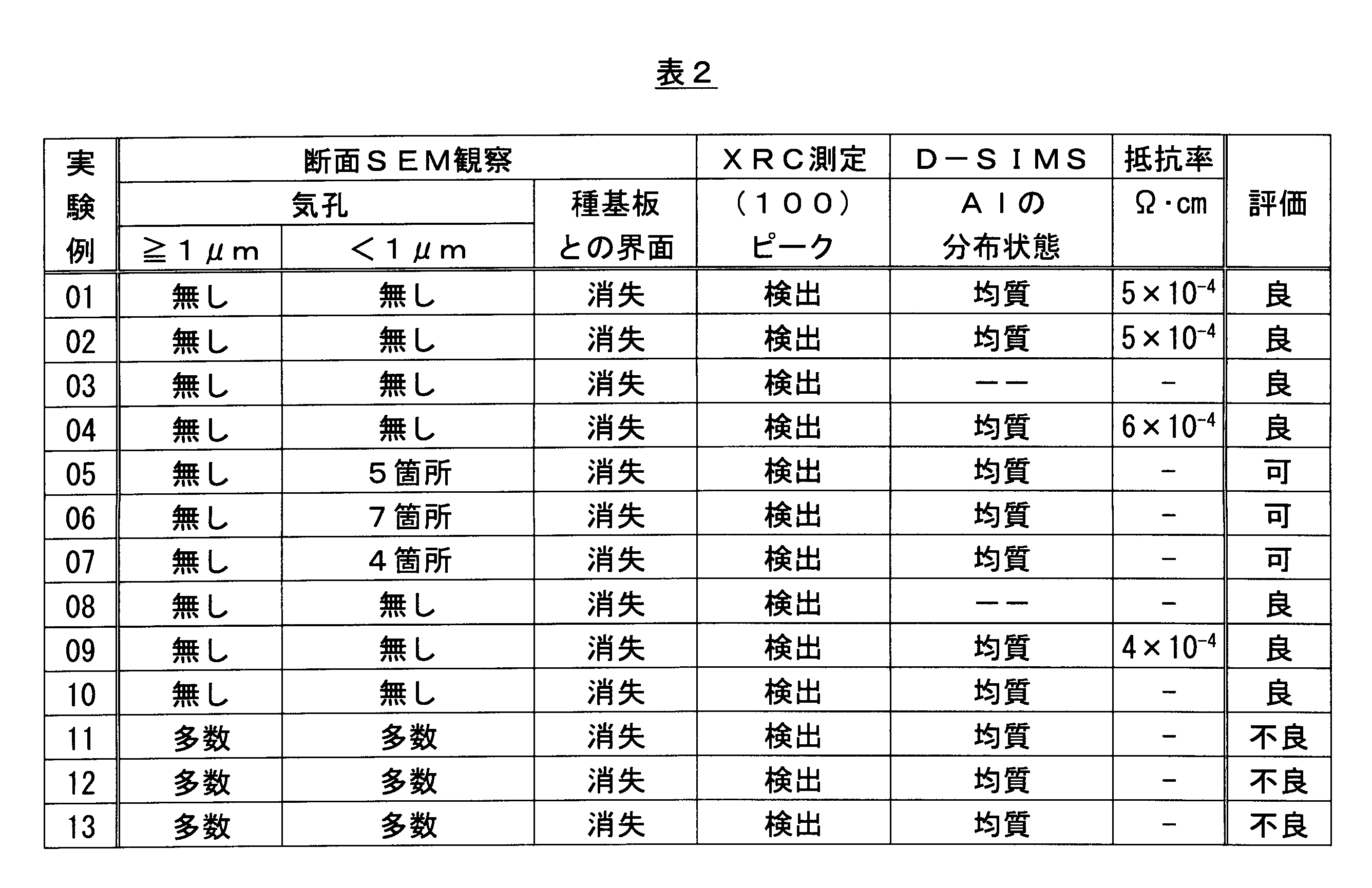
表2に示された評価結果からも明らかであるように、種基板上に堆積された膜の厚みが100μmを超えていたり(実験例11)、加熱ステップにおける昇温速度が30℃/分未満であったり(実験例12)、加熱ステップにおいて膜全体が緩やかに且つ均質に加熱されたり(実験例13)する場合には、多数の気孔が膜内に発生し、緻密な単結晶膜を得ることができないことが確認された。即ち、本発明に係る単結晶製造方法の要件が満たされない場合は、良好な単結晶膜を得ることは困難である。尚、実験例03及び08を除く全ての実験例において、不純物としてのアルミニウム(Al)が0.1~0.3at%の濃度範囲にて膜内に均質に含まれることが確認され、1×10-3Ω・cm以下の非常に低い抵抗率を有する単結晶を得ることができた。
一方、種基板上に堆積された膜の厚みが100μm以下であり、加熱ステップにおける昇温速度が30℃/分以上であり、且つ加熱ステップにおいて膜が種基板の側から加熱されるという本発明に係る単結晶製造方法の要件が満たされる場合は、膜内における気孔の抑制、単結晶化の促進、及び不純物(ドーパント)の均質な分布という観点から見て、許容可能な品質を有する単結晶膜を得ることができた(例えば、実験例05乃至07を参照)。
更に、種基板上に堆積された膜の厚みが30μm以下であり、加熱ステップにおける昇温速度が300℃/分以上であり、且つ加熱ステップにおいて膜が種基板の側から加熱されるという本発明に係る単結晶製造方法のより好ましい要件が満たされる場合は、膜内における気孔の抑制、単結晶化の促進、及び不純物(ドーパント)の均質な分布という観点から見て、極めて良好な品質を有する単結晶膜を得ることができた(例えば、実験例01乃至04、並びに実験例08乃至10を参照)。
本実施例は、成膜ステップにおいて非晶質膜を形成することにより、加熱ステップにおける単結晶化を進行し易くして、原料融液を得ることが容易な材料系のみならず、原料融液を得ることが困難な材料系においても気孔が少ない高品質な単結晶をより高い生産性にて作製することが可能であることを検証することを目的として実施した。
1.評価用試料の作製
(1)成膜ステップ
RFマグネトロンスパッタ装置にて、酸化チタン(TiO2)の単結晶基板(ルチル、10mm×10mm平方、厚さ0.5mm、(100)面)上に、1.5μmの厚みを有する酸化チタン(TiO2)の非晶質層を成膜した。成膜においては、市販の酸化チタン(TiO2)焼結体ターゲットを使用した。また、成膜条件は、純Ar雰囲気中、1Paの圧力及び室温において、投入電力は120W、成膜時間は120分間とした。
(1)成膜ステップ
RFマグネトロンスパッタ装置にて、酸化チタン(TiO2)の単結晶基板(ルチル、10mm×10mm平方、厚さ0.5mm、(100)面)上に、1.5μmの厚みを有する酸化チタン(TiO2)の非晶質層を成膜した。成膜においては、市販の酸化チタン(TiO2)焼結体ターゲットを使用した。また、成膜条件は、純Ar雰囲気中、1Paの圧力及び室温において、投入電力は120W、成膜時間は120分間とした。
(2)加熱ステップ
本実施例においても、上述した実施例1と同様に、図2に示す加熱装置を使用して、上記非晶質膜を加熱した。より詳しくは、種基板202の膜が堆積した面とは反対側から近赤外線を照射して、非晶質膜を種基板側から加熱した。加熱条件は、純Ar雰囲気中にて、1000℃の加熱温度、400℃/分の昇温速度、及び10分の保持時間とした。本実施例に係る試料においても、加熱ステップの前後での膜厚の変化は認められなかった。
本実施例においても、上述した実施例1と同様に、図2に示す加熱装置を使用して、上記非晶質膜を加熱した。より詳しくは、種基板202の膜が堆積した面とは反対側から近赤外線を照射して、非晶質膜を種基板側から加熱した。加熱条件は、純Ar雰囲気中にて、1000℃の加熱温度、400℃/分の昇温速度、及び10分の保持時間とした。本実施例に係る試料においても、加熱ステップの前後での膜厚の変化は認められなかった。
2.各種評価用試料の評価方法
(1)断面SEM観察
上記加熱ステップを経た上記評価用試料につき、上述した実施例1と同様に断面SEM観察を行い、気孔の有無、界面状態について評価した。
(1)断面SEM観察
上記加熱ステップを経た上記評価用試料につき、上述した実施例1と同様に断面SEM観察を行い、気孔の有無、界面状態について評価した。
(2)面内ロッキングカーブ(XRC)測定
上記加熱ステップを経た上記評価用試料につき、上述した実施例1と同様に、面内ロッキングカーブ(XRC)測定を行った。但し、本実施例においては、(001)ピークが検出された場合、緻密な単結晶膜が良好に得られたと判断した。
上記加熱ステップを経た上記評価用試料につき、上述した実施例1と同様に、面内ロッキングカーブ(XRC)測定を行った。但し、本実施例においては、(001)ピークが検出された場合、緻密な単結晶膜が良好に得られたと判断した。
3.各種評価用試料の評価結果
上記加熱ステップを経た上記評価用試料につき、上記評価方法(1)において、研磨断面における膜の端部から40視野を5000倍の倍率にて走査型電子顕微鏡(SEM)観察を行ったが気孔は認められなかった。また、膜と種基板との間の界面が消失していることから、緻密な単結晶膜が良好に得られたと判断された。一方、上記評価方法(2)においては、(001)ピークが検出されたことから、緻密な単結晶膜が良好に得られたと判断された。
上記加熱ステップを経た上記評価用試料につき、上記評価方法(1)において、研磨断面における膜の端部から40視野を5000倍の倍率にて走査型電子顕微鏡(SEM)観察を行ったが気孔は認められなかった。また、膜と種基板との間の界面が消失していることから、緻密な単結晶膜が良好に得られたと判断された。一方、上記評価方法(2)においては、(001)ピークが検出されたことから、緻密な単結晶膜が良好に得られたと判断された。
本実施例における以上の評価結果から、成膜ステップにおいて非晶質膜を形成することにより、加熱ステップにおける単結晶化を進行し易くして、原料融液を得ることが容易な材料系のみならず、原料融液を得ることが困難な材料系においても気孔が少ない高品質な単結晶をより高い生産性にて作製することが可能であることが確認された。
本実施例は、サファイア(Al2O3)基板上に酸化亜鉛(ZnO)の単結晶が成膜された種基板の表面上に、アルミニウム(Al)がドープされた酸化亜鉛(ZnO)の単結晶層を作製することにより、サファイアを種基板として使用した場合と比較して、より高い結晶性を有する単結晶を得ることができることを検証することを目的として実施した。
1.評価用試料の作製
(1)種基板の作製
RS-MBE(ラジカルソース分子線エピタキシー)装置を用いてサファイア基板(10mm×10mm平方、厚さ0.5mm、c面)の表面上に酸化亜鉛(ZnO)の単結晶膜を成膜した。この際、金属材料である亜鉛(Zn)は、クヌーセンセルにおいて照射して支持基板に供給した。ガス材料である酸素(O)は、RFラジカル発生装置において酸素ガス(O2)を原料として用いて、酸素ラジカルとして供給した。それぞれの原料の純度については、亜鉛(Zn)は7N、酸素ガス(O2)は6Nのものを用いた。また、支持基板は抵抗加熱ヒータを用いて700℃に加熱し、亜鉛(Zn)と酸素(O)とが量論比となるようにガスソースのフラックスを制御しながら、厚さ100nmの酸化亜鉛(ZnO)の単結晶層を成膜し、種基板とした。
(2)成膜ステップ及び加熱ステップ
上記(1)において作製した種基板を用いた点を除き、実施例1の実験例10と同様の手順により、アルミニウム(Al)がドープされた酸化亜鉛(ZnO)の単結晶を作製した。具体的には、成膜ステップにおいては、アルミニウム(Al)が固溶している酸化亜鉛(ZnO)粉末をAD法により上記種基板の表面上に成膜し、加熱ステップにおいては、図2に示した加熱装置を使用して、表1に記載した実施例1の実験例10と同じ条件下にて上記膜を加熱した。尚、1サイクルの成膜ステップ及び加熱ステップにより、厚さ2.4μmのアルミニウム(Al)がドープされた酸化亜鉛(ZnO)の単結晶膜が成膜された。同サイクルを100回繰り返すことにより、厚さ240μmのアルミニウム(Al)がドープされた酸化亜鉛(ZnO)の単結晶を作製することができた。
上記(1)において作製した種基板を用いた点を除き、実施例1の実験例10と同様の手順により、アルミニウム(Al)がドープされた酸化亜鉛(ZnO)の単結晶を作製した。具体的には、成膜ステップにおいては、アルミニウム(Al)が固溶している酸化亜鉛(ZnO)粉末をAD法により上記種基板の表面上に成膜し、加熱ステップにおいては、図2に示した加熱装置を使用して、表1に記載した実施例1の実験例10と同じ条件下にて上記膜を加熱した。尚、1サイクルの成膜ステップ及び加熱ステップにより、厚さ2.4μmのアルミニウム(Al)がドープされた酸化亜鉛(ZnO)の単結晶膜が成膜された。同サイクルを100回繰り返すことにより、厚さ240μmのアルミニウム(Al)がドープされた酸化亜鉛(ZnO)の単結晶を作製することができた。
2.評価用試料の評価方法
本実施例においても、実施例1と同様に、以下の評価方法を用いた。
(1)断面SEM観察
得られた単結晶の断面をSEMによって観察し、当該断面における気孔の有無及び単結晶と種基板との界面の状況を評価した。
(2)面内ロッキングカーブ(XRC)測定
面内ロッキングカーブ(XRC)測定により検出された(100)ピークを評価した。
本実施例においても、実施例1と同様に、以下の評価方法を用いた。
(1)断面SEM観察
得られた単結晶の断面をSEMによって観察し、当該断面における気孔の有無及び単結晶と種基板との界面の状況を評価した。
(2)面内ロッキングカーブ(XRC)測定
面内ロッキングカーブ(XRC)測定により検出された(100)ピークを評価した。
3.各種評価用試料の評価結果
上記評価方法(1)において、断面における膜の端部から40視野を5000倍の倍率にて走査型電子顕微鏡(SEM)観察を行ったが気孔は認められなかった。また、膜と種基板との間の界面が消失していた。また、上記評価方法(2)においては、実施例1の実験例10と比較して、よりシャープな(100)ピークが検出された。即ち、本実施例において、実施例1の実験例10と比較して、より高い結晶性を有する単結晶を作製することができた。
上記評価方法(1)において、断面における膜の端部から40視野を5000倍の倍率にて走査型電子顕微鏡(SEM)観察を行ったが気孔は認められなかった。また、膜と種基板との間の界面が消失していた。また、上記評価方法(2)においては、実施例1の実験例10と比較して、よりシャープな(100)ピークが検出された。即ち、本実施例において、実施例1の実験例10と比較して、より高い結晶性を有する単結晶を作製することができた。
本実施例における以上の評価結果から、サファイア(Al2O3)基板上に酸化亜鉛(ZnO)の単結晶層が成膜された種基板を使用することにより、サファイアを種基板として使用した場合と比較して、より高い結晶性を有する単結晶を得ることができることが確認された。
本実施例は、加熱ステップにおいて種基板の反り及び/又はうねりが抑制された状態で熱処理を行うことにより、種基板の反り及び/又はうねりが抑制されない状態で熱処理を行う場合と比較して、より高い品質を有する単結晶を得ることができることを検証することを目的として実施した。
1.評価用試料の作製
(1)種基板の作製及び成膜ステップ
本実施例においては、前述した実施例1の実験例01及び04において使用した種基板及び成膜粉を使用し、それぞれ実施例1の実験例01及び04と同じ条件にて成膜ステップを実施し、種基板の表面上に膜を形成させた。尚、本実施例においては、図4に示されているように、1.5mmの幅を有する市販の固定用テープ40(例えば、カプトン(登録商標)テープ)を使用して、種基板21の周縁部を種基板ホルダ34の表面上に固定し、当該基板の表面上の7mm×7mm平方の領域に対して成膜を行った。斯くして得られた実施例1の実験例01及び04に対応する種基板は、それぞれ50μm及び90μmの反り量(種基板の中央部における浮き上がり)を示した(反り量の測定方法については後述する)。
(2)加熱ステップ
上記(1)において作製した実施例1の実験例01及び04に対応する種基板のそれぞれにつき、前述した実施例1と同様に、図2に示す加熱装置を使用して、加熱ステップを実施し、アルミニウム(Al)がドープされた酸化亜鉛(ZnO)の単結晶を作製した。但し、実験例01及び04に対応する種基板のそれぞれにつき、成膜ステップ後の種基板をセラミックス製の治具を用いて台座に押さえ付けることにより種基板の反り及び/又はうねりを矯正した試料と、かかる矯正を施さない試料とを作製し、それぞれについて加熱ステップを実施した。以降、実験例01及び04に対応する試料のそれぞれにつき、種基板の反り及び/又はうねりを矯正したものを「実験例41及び44」とそれぞれ称し、種基板の反り及び/又はうねりを矯正しなかったものについては単に「実験例01及び04」とそれぞれ称することとする。尚、斯くして種基板の反り及び/又はうねりを矯正した実験例41及び44の種基板は、表3に示すように、それぞれ2μm及び5μmの反り量を示した。更に、実験例01と実験例41との組、及び実験例04と実験例44との組のそれぞれについて、得られた単結晶の品質(欠陥密度)を評価した。
上記(1)において作製した実施例1の実験例01及び04に対応する種基板のそれぞれにつき、前述した実施例1と同様に、図2に示す加熱装置を使用して、加熱ステップを実施し、アルミニウム(Al)がドープされた酸化亜鉛(ZnO)の単結晶を作製した。但し、実験例01及び04に対応する種基板のそれぞれにつき、成膜ステップ後の種基板をセラミックス製の治具を用いて台座に押さえ付けることにより種基板の反り及び/又はうねりを矯正した試料と、かかる矯正を施さない試料とを作製し、それぞれについて加熱ステップを実施した。以降、実験例01及び04に対応する試料のそれぞれにつき、種基板の反り及び/又はうねりを矯正したものを「実験例41及び44」とそれぞれ称し、種基板の反り及び/又はうねりを矯正しなかったものについては単に「実験例01及び04」とそれぞれ称することとする。尚、斯くして種基板の反り及び/又はうねりを矯正した実験例41及び44の種基板は、表3に示すように、それぞれ2μm及び5μmの反り量を示した。更に、実験例01と実験例41との組、及び実験例04と実験例44との組のそれぞれについて、得られた単結晶の品質(欠陥密度)を評価した。
2.各種評価用試料の評価方法
(1)種基板の反り量の測定
上述した成膜ステップを経た各評価用試料につき、小型形状粗さ測定機(Taylor-Hobson社製、「Form Talysurf plus」)を使用して、種基板の反り量を測定した。より詳細には、各種評価用試料の正方形の基板の直交する1組の辺のそれぞれに平行であり且つそれぞれの辺から1mm離れている長さ8mmの線分(図5に示されている両矢印を参照)に沿って基板の裏面(膜が形成された面とは反対側の面)を走査し、それぞれの線分について得られた断面曲線最大高さ(Pt)の平均値を求め、反り量として定義した。
(1)種基板の反り量の測定
上述した成膜ステップを経た各評価用試料につき、小型形状粗さ測定機(Taylor-Hobson社製、「Form Talysurf plus」)を使用して、種基板の反り量を測定した。より詳細には、各種評価用試料の正方形の基板の直交する1組の辺のそれぞれに平行であり且つそれぞれの辺から1mm離れている長さ8mmの線分(図5に示されている両矢印を参照)に沿って基板の裏面(膜が形成された面とは反対側の面)を走査し、それぞれの線分について得られた断面曲線最大高さ(Pt)の平均値を求め、反り量として定義した。
(2)欠陥密度の測定
上述した加熱ステップを経た各評価用試料につき、種基板の主面に直交する平面による断面をTEMによって観察することにより、それぞれの試料において得られた単結晶の欠陥密度を求めた。より詳しくは、上記加熱ステップを経た各評価用試料から、少なくとも種基板と成膜された膜が単結晶化した部分(以降、「単結晶化部」と称する場合がある)との界面を含む切片を切り出し、当該界面付近における切片の厚み(T)が150nmとなるようにイオンミリングによって加工した。斯くして加工された切片の上記界面の周辺を50000倍の倍率にてTEM観察を行い、明視野像を撮影した。
上述した加熱ステップを経た各評価用試料につき、種基板の主面に直交する平面による断面をTEMによって観察することにより、それぞれの試料において得られた単結晶の欠陥密度を求めた。より詳しくは、上記加熱ステップを経た各評価用試料から、少なくとも種基板と成膜された膜が単結晶化した部分(以降、「単結晶化部」と称する場合がある)との界面を含む切片を切り出し、当該界面付近における切片の厚み(T)が150nmとなるようにイオンミリングによって加工した。斯くして加工された切片の上記界面の周辺を50000倍の倍率にてTEM観察を行い、明視野像を撮影した。
上記明視野像中の単結晶化部において、単結晶化部と種基板との界面に平行な長さ(L)5000nmの線分を、上記界面から400nm、800nm、1200nm、1600nm、及び2000nm離れた箇所に計5本引き、これらの線分と重なる位置に存在する格子欠陥の総数(S)をカウントした。斯くして得られた格子欠陥の総数Sから、以下の式(2)に基づいて計算した値(D)[/cm2]を単結晶の欠陥密度(D)[/cm2]としてそれぞれ算出した。各評価用試料について算出された欠陥密度(D)もまた、表3に列挙する。

3.各種評価用試料の評価結果
上記各種評価用試料についての上記評価方法(1)及び(2)の結果を、以下の表3に列挙する。
上記各種評価用試料についての上記評価方法(1)及び(2)の結果を、以下の表3に列挙する。
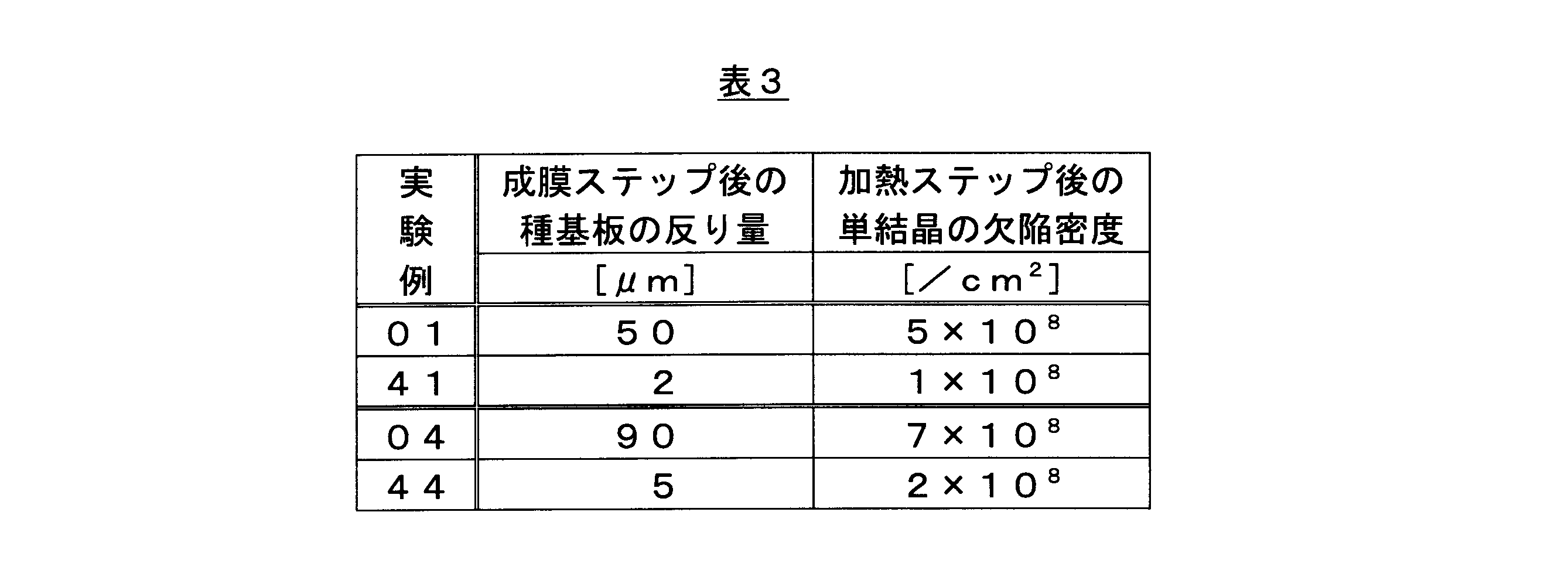
表3に示されているように、本発明に係る単結晶製造方法に含まれる加熱ステップにおいて熱処理に付される実施例1の実験例01に対応する種基板における反り量を50μmから2μmに抑制することにより、結果として得られる単結晶における欠陥密度を5×10⁸個/cm2から1×108個/cm2に低減することができた。同様に、本発明に係る単結晶製造方法に含まれる加熱ステップにおいて熱処理に付される実施例1の実験例04に対応する種基板における反り量を90μmから5μmに抑制することにより、結果として得られる単結晶における欠陥密度を7×108個/cm2から2×108個/cm2に低減することができた。
本実施例における以上の評価結果から、本発明に係る単結晶製造方法に含まれる加熱ステップにおいて当該方法によって得ようとする単結晶の原料を含む膜が表面上に形成された種基板の反り及び/又はうねりを低減することにより、結果として得られる単結晶における格子欠陥を有効に低減して、結果として得られる単結晶の品質を向上させることができることが確認された。
以上、本発明を説明することを目的として、特定の構成を有する幾つかの実施態様について説明してきたが、本発明の範囲は、これらの例示的な実施態様に限定されるものではなく、特許請求の範囲及び明細書に記載された事項の範囲内で、適宜修正を加えることができることは言うまでも無い。
11…キャリアガス、12…成膜粉、20…成膜装置、21…種基板、22…エアロゾル生成部、23…エアロゾル生成室、24…原料供給管、25…加振器、30…成膜部、32…成膜チャンバ、33…X-Yステージ、34…種基板ホルダ、36…噴射ノズル、37…スリット、38…真空ポンプ、40…固定用テープ、201…膜、202…種基板、203…白金板、204…石英製台座、205…熱電対、及び206…近赤外線ランプ。
Claims (23)
- 種基板の表面上に膜を形成する成膜ステップ、及び
前記種基板の表面上に形成された前記膜を加熱して単結晶を得る加熱ステップ、
を含む単結晶製造方法であって、
前記成膜ステップにおいて形成される前記膜の前記種基板の表面に直交する方向における厚みである膜厚が100μm以下であること、
前記加熱ステップにおいて前記膜が前記種基板の側から加熱されること、及び
前記加熱ステップにおける前記膜の昇温速度が30℃/分以上であること、
を特徴とする単結晶製造方法。 - 請求項1に記載の単結晶製造方法であって、
前記成膜ステップにおいて形成される前記膜の膜厚が30μm以下であること、
を特徴とする単結晶製造方法。 - 請求項1又は2の何れか1項に記載の単結晶製造方法であって、
前記加熱ステップにおける前記膜の昇温速度が300℃/分以上であること、
を特徴とする単結晶製造方法。 - 請求項1乃至3の何れか1項に記載の単結晶製造方法であって、
前記成膜ステップにおいて前記種基板の表面上に前記膜を形成する方法が、粉末法、溶液法、物理蒸着(PVD)法、及び化学蒸着(CVD)法からなる群より選ばれる何れかの方法であること、
を特徴とする単結晶製造方法。 - 請求項4に記載の単結晶製造方法であって、
前記粉末法がエアロゾルデポジション法(AD法)及びパウダージェットデポジション法(PJD法)からなる群より選ばれる何れかの方法であり、前記溶液法が、液相析出法、スピンコーティング法、及びディッピング法からなる群より選ばれる何れかの方法であり、前記物理蒸着(PVD)法がスパッタ法であり、前記化学蒸着(CVD)法がミストCVD法及びレーザーCVD法からなる群より選ばれる何れかの方法であること、
を特徴とする単結晶製造方法。 - 請求項1乃至5の何れか1項に記載の単結晶製造方法であって、
前記加熱ステップにおいて前記種基板の表面上に形成された前記膜を加熱する方法が、赤外線ランプ、レーザー、高周波電磁波からなる群より選ばれる何れかの熱源を使用する加熱方法であること、
を特徴とする単結晶製造方法。 - 請求項1乃至6の何れか1項に記載の単結晶製造方法であって、
前記成膜ステップにおいて形成される前記膜が非晶質であること、
を特徴とする単結晶製造方法。 - 請求項1乃至7の何れか1項に記載の単結晶製造方法であって、
前記膜の主成分が、酸化物及び窒化物、並びにそれらの先駆物質からなる群より選ばれる何れか1種の材料であること、
を特徴とする単結晶製造方法。 - 請求項8に記載の単結晶製造方法であって、
前記酸化物が酸化亜鉛(ZnO)及び酸化チタン(TiO2)であり、前記窒化物が窒化ガリウム(GaN)であること、
を特徴とする単結晶製造方法。 - 請求項1乃至9の何れか1項に記載の単結晶製造方法であって、
前記種基板が、単結晶層が表面上に成膜された基板であること、及び
前記単結晶層の表面上に前記膜が形成されること、
を特徴とする単結晶製造方法。 - 請求項1乃10の何れか1項に記載の単結晶製造方法であって、
前記加熱ステップにおいて、前記種基板の断面曲線最大高さ(Pt)が5μm以下である状態で、前記膜を加熱すること、
を特徴とする単結晶製造方法。 - 請求項1乃至11の何れか1項に記載の単結晶製造方法であって、
前記種基板又は前記単結晶層の主成分が、酸化亜鉛(ZnO)、窒化ガリウム(GaN)、酸化チタン(TiO2)、及びサファイアからなる群より選ばれる何れか1種の材料であること、
を特徴とする単結晶製造方法。 - 請求項1乃至11の何れか1項に記載の単結晶製造方法であって、
前記種基板又は前記単結晶層の主成分が、酸化マグネシウム(MgO)、酸化カドミウム(CdO)、硫化亜鉛(ZnS)、及びテルル化亜鉛(ZnTe)からなる群より選ばれる1種以上と酸化亜鉛(ZnO)との混晶、又は窒化アルミニウム(AlN)及び窒化インジウム(InN)からなる群より選ばれる1種以上と窒化ガリウム(GaN)との混晶、であること、
を特徴とする単結晶製造方法。 - 請求項1乃至13の何れか1項に記載の単結晶製造方法であって、
前記膜が、アルミニウム(Al)、ガリウム(Ga)、インジウム(In)、窒素(N)、硼素(B)、リン(P)、砒素(As)、フッ素(F)、塩素(Cl)、臭素(Br)、ヨウ素(I)、カーボン(C)、シリコン(Si)、硫黄(S)、リチウム(Li)、ナトリウム(Na)、カリウム(K)、マグネシウム(Mg)、カドミウム(Cd)、セレン(Se)、テルル(Te)、銀(Ag)、ニオブ(Nb)、及び銅(Cu)からなる群より選ばれる少なくとも何れか1種以上の元素を不純物として含むこと、
を特徴とする単結晶製造方法。 - 請求項1乃至14の何れか1項に記載の単結晶製造方法であって、
前記膜が、酸化マグネシウム(MgO)、酸化カドミウム(CdO)、硫化亜鉛(ZnS)、及びテルル化亜鉛(ZnTe)からなる群より選ばれる1種以上と酸化亜鉛(ZnO)との混晶及び/又は混合物、あるいは窒化アルミニウム(AlN)及び窒化インジウム(InN)からなる群より選ばれる1種以上と窒化ガリウム(GaN)との混晶及び/又は混合物、を含んでなること、
を特徴とする単結晶製造方法。 - 請求項1乃至15の何れか1項に記載の単結晶製造方法を繰り返し実行することによって単結晶を得ること、
を特徴とする単結晶製造方法。 - 請求項1乃至14及び請求項16の何れか1項に記載の単結晶製造方法によって得られること、
を特徴とする酸化亜鉛(ZnO)単結晶。 - 請求項17に記載の酸化亜鉛(ZnO)単結晶であって、
前記成膜ステップにおいて形成される前記膜の前記種基板の表面に直交する方向における当該結晶の厚みである結晶厚が30μmを超えること、
を特徴とする酸化亜鉛(ZnO)単結晶。 - 請求項18に記載の酸化亜鉛(ZnO)単結晶であって、
請求項16に記載の単結晶製造方法によって得られること、及び
前記成膜ステップにおいて形成される前記膜の前記種基板の表面に直交する方向における当該結晶の厚みである結晶厚が100μmを超えること、
を特徴とする酸化亜鉛(ZnO)単結晶。 - 請求項17乃至19の何れか1項に記載の酸化亜鉛(ZnO)単結晶であって、
アルミニウム(Al)、ガリウム(Ga)、及びインジウム(In)からなる群より選ばれる少なくとも何れか1種以上の元素を不純物として含むこと、並びに
前記不純物の含有率が0.02at%以上であること、
を特徴とする酸化亜鉛(ZnO)単結晶。 - 請求項20に記載の酸化亜鉛(ZnO)単結晶であって、
前記不純物の含有率が0.1at%以上であること、
を特徴とする酸化亜鉛(ZnO)単結晶。 - 請求項17乃至21の何れか1項に記載の酸化亜鉛(ZnO)単結晶であって、
抵抗率が1×10⁻³Ω・cm以下であること、
を特徴とする酸化亜鉛(ZnO)単結晶。 - 請求項15又は16の何れか1項に記載の単結晶製造方法によって得られること、並びに
酸化マグネシウム(MgO)、酸化カドミウム(CdO)、硫化亜鉛(ZnS)、及びテルル化亜鉛(ZnTe)からなる群より選ばれる1種以上と酸化亜鉛(ZnO)との混晶であるか、又は窒化アルミニウム(AlN)及び窒化インジウム(InN)からなる群より選ばれる1種以上と窒化ガリウム(GaN)との混晶であること、
を特徴とする単結晶。
Priority Applications (1)
| Application Number | Priority Date | Filing Date | Title |
|---|---|---|---|
| JP2014551993A JPWO2014091968A1 (ja) | 2012-12-14 | 2013-12-03 | 単結晶製造方法、及び当該方法によって製造される単結晶 |
Applications Claiming Priority (8)
| Application Number | Priority Date | Filing Date | Title |
|---|---|---|---|
| JP2012273556 | 2012-12-14 | ||
| JP2012-273556 | 2012-12-14 | ||
| JP2013040277 | 2013-03-01 | ||
| JP2013-040277 | 2013-03-01 | ||
| JP2013-128184 | 2013-06-19 | ||
| JP2013128184 | 2013-06-19 | ||
| JP2013205550 | 2013-09-30 | ||
| JP2013-205550 | 2013-09-30 |
Publications (1)
| Publication Number | Publication Date |
|---|---|
| WO2014091968A1 true WO2014091968A1 (ja) | 2014-06-19 |
Family
ID=50934260
Family Applications (1)
| Application Number | Title | Priority Date | Filing Date |
|---|---|---|---|
| PCT/JP2013/082493 Ceased WO2014091968A1 (ja) | 2012-12-14 | 2013-12-03 | 単結晶製造方法、及び当該方法によって製造される単結晶 |
Country Status (2)
| Country | Link |
|---|---|
| JP (1) | JPWO2014091968A1 (ja) |
| WO (1) | WO2014091968A1 (ja) |
Cited By (7)
| Publication number | Priority date | Publication date | Assignee | Title |
|---|---|---|---|---|
| JP2016130350A (ja) * | 2015-01-14 | 2016-07-21 | サムソン エレクトロ−メカニックス カンパニーリミテッド. | コーティング膜を備える構造体およびその製造方法 |
| KR20200102266A (ko) * | 2019-02-21 | 2020-08-31 | 광운대학교 산학협력단 | 에어로졸 증착을 통한 니어 제로 TCR 및 고 접합 강도를 갖는 TiO2/Cu 복합 합성 필름의 제조 방법 |
| CN113279058A (zh) * | 2021-04-13 | 2021-08-20 | 中国科学院上海技术物理研究所 | 一种低对称性层状材料Te的可控制备方法 |
| JP2022513852A (ja) * | 2018-12-21 | 2022-02-09 | アールエフ360・ヨーロップ・ゲーエムベーハー | 圧電材料および圧電デバイス |
| JPWO2022215621A1 (ja) * | 2021-04-07 | 2022-10-13 | ||
| CN115198356A (zh) * | 2022-07-15 | 2022-10-18 | 郑州大学 | 一种特定取向的大规格金属单晶及其制备方法 |
| KR20230102576A (ko) * | 2021-12-30 | 2023-07-07 | 주식회사 하이퍼머티리얼즈 | 에피택셜 막 형성 방법 및 이에 따른 에피택셜 막 구조 |
Citations (8)
| Publication number | Priority date | Publication date | Assignee | Title |
|---|---|---|---|---|
| JPH07138094A (ja) * | 1993-11-16 | 1995-05-30 | Ngk Insulators Ltd | 酸化亜鉛単結晶の育成方法 |
| JPH09249962A (ja) * | 1996-03-14 | 1997-09-22 | Toshiba Corp | 酸化物薄膜の形成方法および酸化物薄膜 |
| JPH11199393A (ja) * | 1998-01-16 | 1999-07-27 | Fuji Xerox Co Ltd | 強誘電体薄膜素子の作製方法 |
| JP2004292239A (ja) * | 2003-03-27 | 2004-10-21 | Murata Mfg Co Ltd | 強誘電体薄膜素子の製造方法 |
| JP2006188046A (ja) * | 2004-12-09 | 2006-07-20 | Fuji Photo Film Co Ltd | セラミックス膜の製造方法及びセラミックス膜を含む構造物 |
| JP2006298747A (ja) * | 2005-03-22 | 2006-11-02 | Fuji Photo Film Co Ltd | 配向膜の製造方法、及び、液体吐出ヘッドの製造方法 |
| JP2009234824A (ja) * | 2008-03-26 | 2009-10-15 | Mitsubishi Gas Chem Co Inc | 自立Mg含有ZnO系混晶単結晶ウエファーおよびそれに用いるMg含有ZnO系混晶単結晶の製造方法 |
| WO2012060309A1 (ja) * | 2010-11-02 | 2012-05-10 | 日本碍子株式会社 | 結晶製造方法 |
-
2013
- 2013-12-03 JP JP2014551993A patent/JPWO2014091968A1/ja active Pending
- 2013-12-03 WO PCT/JP2013/082493 patent/WO2014091968A1/ja not_active Ceased
Patent Citations (8)
| Publication number | Priority date | Publication date | Assignee | Title |
|---|---|---|---|---|
| JPH07138094A (ja) * | 1993-11-16 | 1995-05-30 | Ngk Insulators Ltd | 酸化亜鉛単結晶の育成方法 |
| JPH09249962A (ja) * | 1996-03-14 | 1997-09-22 | Toshiba Corp | 酸化物薄膜の形成方法および酸化物薄膜 |
| JPH11199393A (ja) * | 1998-01-16 | 1999-07-27 | Fuji Xerox Co Ltd | 強誘電体薄膜素子の作製方法 |
| JP2004292239A (ja) * | 2003-03-27 | 2004-10-21 | Murata Mfg Co Ltd | 強誘電体薄膜素子の製造方法 |
| JP2006188046A (ja) * | 2004-12-09 | 2006-07-20 | Fuji Photo Film Co Ltd | セラミックス膜の製造方法及びセラミックス膜を含む構造物 |
| JP2006298747A (ja) * | 2005-03-22 | 2006-11-02 | Fuji Photo Film Co Ltd | 配向膜の製造方法、及び、液体吐出ヘッドの製造方法 |
| JP2009234824A (ja) * | 2008-03-26 | 2009-10-15 | Mitsubishi Gas Chem Co Inc | 自立Mg含有ZnO系混晶単結晶ウエファーおよびそれに用いるMg含有ZnO系混晶単結晶の製造方法 |
| WO2012060309A1 (ja) * | 2010-11-02 | 2012-05-10 | 日本碍子株式会社 | 結晶製造方法 |
Cited By (12)
| Publication number | Priority date | Publication date | Assignee | Title |
|---|---|---|---|---|
| JP2016130350A (ja) * | 2015-01-14 | 2016-07-21 | サムソン エレクトロ−メカニックス カンパニーリミテッド. | コーティング膜を備える構造体およびその製造方法 |
| JP2022513852A (ja) * | 2018-12-21 | 2022-02-09 | アールエフ360・ヨーロップ・ゲーエムベーハー | 圧電材料および圧電デバイス |
| KR20200102266A (ko) * | 2019-02-21 | 2020-08-31 | 광운대학교 산학협력단 | 에어로졸 증착을 통한 니어 제로 TCR 및 고 접합 강도를 갖는 TiO2/Cu 복합 합성 필름의 제조 방법 |
| KR102207355B1 (ko) * | 2019-02-21 | 2021-01-22 | 광운대학교 산학협력단 | 에어로졸 증착을 통한 니어 제로 TCR 및 고 접합 강도를 갖는 TiO2/Cu 복합 합성 필름의 제조 방법 |
| JPWO2022215621A1 (ja) * | 2021-04-07 | 2022-10-13 | ||
| WO2022215621A1 (ja) * | 2021-04-07 | 2022-10-13 | 信越化学工業株式会社 | 積層体の製造方法、積層体の製造装置、積層体及び半導体装置 |
| JP7614336B2 (ja) | 2021-04-07 | 2025-01-15 | 信越化学工業株式会社 | 積層体の製造方法、積層体の製造装置、積層体及び半導体装置 |
| US12660520B2 (en) | 2021-04-07 | 2026-06-16 | Shin-Etsu Chemical Co., Ltd. | Method for producing laminate, producing apparatus for laminate, laminate, and semiconductor device |
| CN113279058A (zh) * | 2021-04-13 | 2021-08-20 | 中国科学院上海技术物理研究所 | 一种低对称性层状材料Te的可控制备方法 |
| KR20230102576A (ko) * | 2021-12-30 | 2023-07-07 | 주식회사 하이퍼머티리얼즈 | 에피택셜 막 형성 방법 및 이에 따른 에피택셜 막 구조 |
| KR102725129B1 (ko) * | 2021-12-30 | 2024-11-04 | 박재혁 | 에피택셜 막 형성 방법 및 이에 따른 에피택셜 막 구조 |
| CN115198356A (zh) * | 2022-07-15 | 2022-10-18 | 郑州大学 | 一种特定取向的大规格金属单晶及其制备方法 |
Also Published As
| Publication number | Publication date |
|---|---|
| JPWO2014091968A1 (ja) | 2017-01-12 |
Similar Documents
| Publication | Publication Date | Title |
|---|---|---|
| JPWO2014091968A1 (ja) | 単結晶製造方法、及び当該方法によって製造される単結晶 | |
| Hong et al. | Room-temperature, texture-controlled growth of ZnO thin films and their application for growing aligned ZnO nanowire arrays | |
| JP7461851B2 (ja) | 半導体膜 | |
| US12159907B2 (en) | Semiconductor film | |
| CN114761629B (zh) | 双轴取向SiC复合基板以及半导体器件用复合基板 | |
| US20210408242A1 (en) | Semiconductor film | |
| US11942520B2 (en) | Semiconductor film | |
| EP3929336A1 (en) | Gan crystal and substrate | |
| US12421621B2 (en) | Underlying substrate | |
| WO2009131063A1 (ja) | Si(1-v-w-x)CwAlxNv基材の製造方法、エピタキシャルウエハの製造方法、Si(1-v-w-x)CwAlxNv基材およびエピタキシャルウエハ | |
| JP7439117B2 (ja) | 下地基板及びその製造方法 | |
| Fan et al. | A low-temperature evaporation route for ZnO nanoneedles and nanosaws | |
| WO2020261574A1 (ja) | 半導体膜 | |
| WO2014091969A1 (ja) | 単結晶製造装置、当該装置を用いる単結晶製造方法、及び当該方法によって製造される単結晶 | |
| TW202210669A (zh) | GaN結晶及GaN基板 | |
| JP7108783B2 (ja) | 半導体膜 | |
| Nakamura et al. | Influence of Sb on a controlled-growth of aligned ZnO nanowires in nanoparticle-assisted pulsed-laser deposition | |
| JP4919401B2 (ja) | 素子基板とその製造方法 | |
| Zhao et al. | Structural and optical properties of nanostructured ZnO thin films deposited on quartz glass | |
| Adawiah et al. | Study the Effect of Annealing Temperature on Optical and Structural Properties of Zinc Oxide Thin Film Prepared by Thermal Chemical Vapor Deposition |
Legal Events
| Date | Code | Title | Description |
|---|---|---|---|
| 121 | Ep: the epo has been informed by wipo that ep was designated in this application |
Ref document number: 13862015 Country of ref document: EP Kind code of ref document: A1 |
|
| ENP | Entry into the national phase |
Ref document number: 2014551993 Country of ref document: JP Kind code of ref document: A |
|
| NENP | Non-entry into the national phase |
Ref country code: DE |
|
| 122 | Ep: pct application non-entry in european phase |
Ref document number: 13862015 Country of ref document: EP Kind code of ref document: A1 |