WO2014091843A1 - コンバータ装置 - Google Patents
コンバータ装置 Download PDFInfo
- Publication number
- WO2014091843A1 WO2014091843A1 PCT/JP2013/080162 JP2013080162W WO2014091843A1 WO 2014091843 A1 WO2014091843 A1 WO 2014091843A1 JP 2013080162 W JP2013080162 W JP 2013080162W WO 2014091843 A1 WO2014091843 A1 WO 2014091843A1
- Authority
- WO
- WIPO (PCT)
- Prior art keywords
- duty
- current
- timing
- sampling
- reactor
- Prior art date
- Legal status (The legal status is an assumption and is not a legal conclusion. Google has not performed a legal analysis and makes no representation as to the accuracy of the status listed.)
- Ceased
Links
Images




Classifications
-
- H—ELECTRICITY
- H02—GENERATION; CONVERSION OR DISTRIBUTION OF ELECTRIC POWER
- H02M—APPARATUS FOR CONVERSION BETWEEN AC AND AC, BETWEEN AC AND DC, OR BETWEEN DC AND DC, AND FOR USE WITH MAINS OR SIMILAR POWER SUPPLY SYSTEMS; CONVERSION OF DC OR AC INPUT POWER INTO SURGE OUTPUT POWER; CONTROL OR REGULATION THEREOF
- H02M7/00—Conversion of AC power input into DC power output; Conversion of DC power input into AC power output
- H02M7/42—Conversion of DC power input into AC power output without possibility of reversal
- H02M7/44—Conversion of DC power input into AC power output without possibility of reversal by static converters
- H02M7/48—Conversion of DC power input into AC power output without possibility of reversal by static converters using discharge tubes with control electrode or semiconductor devices with control electrode
- H02M7/53—Conversion of DC power input into AC power output without possibility of reversal by static converters using discharge tubes with control electrode or semiconductor devices with control electrode using devices of a triode or transistor type requiring continuous application of a control signal
- H02M7/537—Conversion of DC power input into AC power output without possibility of reversal by static converters using discharge tubes with control electrode or semiconductor devices with control electrode using devices of a triode or transistor type requiring continuous application of a control signal using semiconductor devices only, e.g. single switched pulse inverters
-
- H—ELECTRICITY
- H02—GENERATION; CONVERSION OR DISTRIBUTION OF ELECTRIC POWER
- H02M—APPARATUS FOR CONVERSION BETWEEN AC AND AC, BETWEEN AC AND DC, OR BETWEEN DC AND DC, AND FOR USE WITH MAINS OR SIMILAR POWER SUPPLY SYSTEMS; CONVERSION OF DC OR AC INPUT POWER INTO SURGE OUTPUT POWER; CONTROL OR REGULATION THEREOF
- H02M3/00—Conversion of DC power input into DC power output
- H02M3/02—Conversion of DC power input into DC power output without intermediate conversion into AC
- H02M3/04—Conversion of DC power input into DC power output without intermediate conversion into AC by static converters
- H02M3/10—Conversion of DC power input into DC power output without intermediate conversion into AC by static converters using discharge tubes with control electrode or semiconductor devices with control electrode
- H02M3/145—Conversion of DC power input into DC power output without intermediate conversion into AC by static converters using discharge tubes with control electrode or semiconductor devices with control electrode using devices of a triode or transistor type requiring continuous application of a control signal
- H02M3/155—Conversion of DC power input into DC power output without intermediate conversion into AC by static converters using discharge tubes with control electrode or semiconductor devices with control electrode using devices of a triode or transistor type requiring continuous application of a control signal using semiconductor devices only
- H02M3/156—Conversion of DC power input into DC power output without intermediate conversion into AC by static converters using discharge tubes with control electrode or semiconductor devices with control electrode using devices of a triode or transistor type requiring continuous application of a control signal using semiconductor devices only with automatic control of output voltage or current, e.g. switching regulators
-
- H—ELECTRICITY
- H02—GENERATION; CONVERSION OR DISTRIBUTION OF ELECTRIC POWER
- H02M—APPARATUS FOR CONVERSION BETWEEN AC AND AC, BETWEEN AC AND DC, OR BETWEEN DC AND DC, AND FOR USE WITH MAINS OR SIMILAR POWER SUPPLY SYSTEMS; CONVERSION OF DC OR AC INPUT POWER INTO SURGE OUTPUT POWER; CONTROL OR REGULATION THEREOF
- H02M1/00—Details of apparatus for conversion
- H02M1/0003—Details of control, feedback or regulation circuits
- H02M1/0009—Devices or circuits for detecting current in a converter
Definitions
- This disclosure relates to a converter device.
- regulates the timing of ON / OFF switching of the switching element of a converter apparatus is determined based on the reactor current etc. which flow into a reactor, suitable sampling timing of the reactor current for calculating the duty of the next period Depends on the duty of the current cycle. Therefore, depending on the duty set in the current cycle, the appropriate sampling timing of the reactor current may be delayed. In such a case, the duty of the next cycle cannot be calculated based on the sampled reactor current until the next duty setting timing. there is a possibility.
- An object of the present invention is to provide a converter device capable of performing the above.
- a converter having a switching element and a reactor; A duty is set for each predetermined duty setting period corresponding to a half cycle of the carrier signal, and ON / OFF switching of the switching element of the converter is executed at a switching timing corresponding to the relationship between the set duty and the carrier signal.
- a control device The control device completes sampling the current value flowing through the reactor by the next duty setting timing and calculating the duty set at the next duty setting timing based on the sampled current value.
- a converter device characterized by determining a duty to be set in the current duty setting cycle is provided.
- the current value of the reactor is sampled at an appropriate sampling timing by the next duty setting timing, and can be set at the next duty setting timing based on the sampled current value.
- a converter device capable of calculating is obtained.
- FIG. 3 is a diagram illustrating an example of a control block 500 of the DC / DC converter 20 in the semiconductor drive device 50.
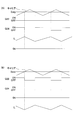
- FIG. It is a figure which shows an example of the time series of the ON / OFF state of switching element Q22, Q24 which switches by the relationship between a carrier signal and a duty.
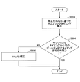
- It is explanatory drawing which shows an example of the correction method of the duty in the duty correction part 512.
- FIG. It is explanatory drawing of FIG.
- FIG. 1 is a diagram showing an example of the overall configuration of a motor drive system 1 for an electric vehicle.
- the motor drive system 1 is a system that drives a vehicle by driving a traveling motor 40 using electric power of a battery 10.
- the electric vehicle typically includes a hybrid vehicle (HV) whose power source is an engine and a traveling motor 40, and an electric vehicle whose power source is only the traveling motor 40.
- HV hybrid vehicle
- the motor drive system 1 includes a battery 10, a DC / DC converter 20, an inverter 30, a travel motor 40, and a semiconductor drive device 50, as shown in FIG.
- the battery 10 is an arbitrary power storage device that stores electric power and outputs a DC voltage, and may be composed of a capacitive element such as a nickel metal hydride battery, a lithium ion battery, or an electric double layer capacitor.
- the DC / DC converter 20 may be a bidirectional DC / DC converter (a reversible chopper type step-up DC / DC converter).
- the DC / DC converter 20 may be capable of step-up conversion from 200 V to 650 V and step-down conversion from 650 V to 200 V, for example.
- a smoothing capacitor C1 may be connected between the input side of the reactor L1 of the DC / DC converter 20 and the negative electrode line.
- the DC / DC converter 20 includes two switching elements Q22 and Q24 and a reactor L1.
- the two switching elements Q22 and Q24 are connected in series between the positive electrode line and the negative electrode line of the inverter 30.
- Reactor L1 is connected in series to the positive electrode side of battery 10.
- Reactor L1 has an output side connected to a connection portion between two switching elements Q22 and Q24.
- the two switching elements Q22 and Q24 of the DC / DC converter 20 are IGBTs (Insulated Gate Bipolar). Transistor).
- the switching elements Q22 and Q24 may be normal IGBTs using diodes (for example, freewheeling diodes) D22 and 24 as external elements, or reverse conducting IGBTs (RC (Reverse Conducting) with diodes D22 and 24 incorporated therein. ) -IGBT).
- the collector of the switching element Q22 of the upper arm is connected to the positive line of the inverter 30, and the emitter of the switching element Q22 of the upper arm is connected to the collector of the switching element Q24 of the lower arm.
- the emitter of the switching element Q24 in the lower arm is connected to the negative electrode line of the inverter 30 and the negative electrode of the battery 10.
- the switching elements Q22 and Q24 may be switching elements other than the IGBT, such as a MOSFET (Metal Oxide Semiconductor Field-Effect Transistor).
- the inverter 30 includes U-phase, V-phase, and W-phase arms arranged in parallel with each other between the positive electrode line and the negative electrode line.
- the U-phase arm consists of a series connection of switching elements (IGBTs) Q1 and Q2
- the V-phase arm consists of a series connection of switching elements (IGBTs in this example) Q3 and Q4, and the W-phase arm
- IGBT switching elements
- diodes D1 to D6 are arranged between the collectors and emitters of the switching elements Q1 to Q6 so that current flows from the emitter side to the collector side, respectively.
- Switching elements Q1 to Q6 may be switching elements other than IGBTs such as MOSFETs.
- the traveling motor 40 is a three-phase permanent magnet motor, and one end of three coils of U, V, and W phases are commonly connected at a midpoint.
- the other end of the U-phase coil is connected to the midpoint M1 of the switching elements Q1 and Q2
- the other end of the V-phase coil is connected to the midpoint M2 of the switching elements Q3 and Q4
- the other end of the W-phase coil is Connected to midpoint M3 of switching elements Q5, Q6.
- a smoothing capacitor C2 is connected between the collector of the switching element Q1 and the negative electrode line.
- the traveling motor 40 may be a hybrid three-phase motor in which an electromagnet and a permanent magnet are combined.
- a second travel motor or generator may be added in parallel.
- a corresponding inverter may be added in parallel.
- the semiconductor drive device 50 controls the DC / DC converter 20.
- the semiconductor drive device 50 may control the inverter 30 in addition to the DC / DC converter 20.
- the semiconductor drive device 50 may be embodied as an ECU (electronic control unit) including a microcomputer.
- ECU electronic control unit
- various functions (including functions described below) of the semiconductor drive device 50 may be realized by arbitrary hardware, software, firmware, or a combination thereof.
- the various functions of the semiconductor drive device 50 are ASIC (application-specific for specific applications) integrated circuit) or FPGA (Field Programmable Gate Array).
- Various functions of the semiconductor drive device 50 may be realized in cooperation with a plurality of ECUs.
- the outline of the control method of the DC / DC converter 20 may be arbitrary.
- the semiconductor drive device 50 controls the DC / DC converter 20 according to the operation (power running or regeneration) of the inverter 30. For example, during power running, the semiconductor drive device 50 switches on / off only the switching element Q24 of the lower arm of the DC / DC converter 20 (one arm drive by the lower arm), boosts the voltage of the battery 10, and increases the inverter 30. Output to the side.
- the switching element Q24 of the lower arm may be controlled by PWM (Pulse Width Modulation).
- the switching element Q22 of the upper arm of the DC / DC converter 20 is switched on / off (one arm drive by the upper arm), and the voltage on the inverter 30 side is stepped down and output to the battery 10 side.
- the switching element Q22 of the upper arm may be PWM controlled.
- the semiconductor drive device 50 may drive the two switching elements Q22 and Q24 on / off in opposite phases (both arm drive).
- FIG. 2 is a diagram illustrating an example of a control block 500 of the DC / DC converter 20 in the semiconductor drive device 50. 2 also shows parts (motor control unit 540 and travel control unit 560) related to the control block 500 of the DC / DC converter 20.
- the motor control unit 540 and the travel control unit 560 may be realized by an ECU that realizes the control block 500, or may be realized by an ECU different from the ECU that realizes the control block 500.
- the traveling control unit 560 may determine a motor torque command value (target drive torque) based on, for example, the accelerator opening and the vehicle speed, and supply the motor torque command value to the motor control unit 540.
- the motor control unit 540 determines the switching elements Q1 to Q6 of the inverter 30 based on the motor torque command value, various sensor values, etc. (for example, the detected value of each phase current by the current sensor or the detected value of the motor rotation speed by the resolver).
- a gate signal (motor gate signal) for on / off switching may be generated.
- the motor gate signal may be applied to the gates of the switching elements Q1 to Q6.
- the control block 500 of the DC / DC converter 20 includes a filter 502, an ADC (Analog-to-Digital Converter) 504, a current control unit 506, a voltage control unit 508, a motor target voltage calculation unit 510, and a duty correction unit. 512, a carrier generation unit 513, a gate signal generation unit 514, and a sampling timing calculation unit 516 may be included.
- ADC Analog-to-Digital Converter
- the filter 502 receives a detection signal (analog signal) from a current sensor (not shown) that detects a current flowing through the reactor L1 (hereinafter also referred to as a reactor current IL).
- the filter 502 filters the detection signal and outputs it to the ADC 504.
- the ADC 504 is activated in accordance with the sampling timing generated by the sampling timing calculation unit 516, samples the detection signal from the filter 502, and obtains a sampling value (digital value) of the reactor current IL.
- the sampling value of the reactor current IL is supplied to the current control unit 506.
- the current control unit 506 drives the switching elements Q22 and Q24 of the DC / DC converter 20 based on the sampling value of the reactor current IL from the ADC 504 and the target value IL * of the reactor current IL from the voltage control unit 508 ( Calculate the duty for switching on / off.
- PI Proportional Integral
- PID Proportional Integral Derivative
- the calculated duty is supplied to the duty correction unit 512.
- the target value IL * of the reactor current IL may be calculated by the voltage control unit 508 based on the motor target voltage VH * and the detected value (VH sensor value) of the voltage VH across the smoothing capacitor C2.
- the motor target voltage VH * is a target value of the voltage VH across the smoothing capacitor C2 (see FIG. 1).
- the motor target voltage VH * may be calculated based on the motor rotational speed and the motor torque command value from the motor control unit 540.
- the duty correction unit 512 corrects the duty from the current control unit 506 and calculates a final duty (after-duty). An example of a correction method by the duty correction unit 512 will be described later.
- the final duty is supplied to the sampling timing calculation unit 516.
- the carrier generation unit 513 generates a reference signal having a predetermined frequency as a carrier signal.
- the carrier signal may have a triangular wave or rectangular wave waveform.
- the frequency of the carrier signal may be constant or variable.
- the frequency of the carrier signal may be varied in a manner that decreases when the temperature of the DC / DC converter 20 increases.
- the carrier signal is supplied to the gate signal generation unit 514 and the sampling timing calculation unit 516.
- the gate signal generation unit 514 is a gate signal for on / off switching of the switching elements Q22 and Q24 of the DC / DC converter 20 based on the carrier signal from the carrier generation unit 513 and the duty from the duty correction unit 512. Is generated.
- the gate signal is applied to each gate of switching elements Q22 and Q24.
- the sampling timing calculation unit 516 determines the sampling timing for sampling (detecting) the reactor current IL based on the carrier signal from the carrier generation unit 513 and the duty from the duty correction unit 512, and the determined sampling A signal indicating timing is transmitted to the ADC 504.
- the sampling timing is determined so that sampling is performed once every on / off switching period of the switching elements Q22 and Q24. At this time, the sampling timing is determined so that the average value of the reactor current IL during the on / off period is sampled.
- An example of a sampling timing determination method will be described later.
- FIG. 3 is a diagram illustrating an example of a time series of the on / off states of the switching elements Q22 and Q24 that are switched depending on the relationship between the carrier signal and the duty.
- FIG. 3A illustrates the relationship between the carrier signal and the duty from the upper stage.
- FIG. 3 is a diagram schematically showing an example of the on / off state of switching elements Q22 and Q24 during powering and the waveform of reactor current IL, and
- FIG. 3B shows the relationship between the carrier signal and the duty, It is a figure which shows roughly an example of the waveform of the ON / OFF state of switching elements Q22 and Q24 at the time of regeneration, and the reactor current IL.
- the reactor current IL is smaller than a predetermined value Th2, as shown in FIG. 3B, only the upper arm switching element Q22 is turned on / off, and the lower arm switching element Q24 is turned off. It may be maintained in a state (one arm drive by the upper arm).
- the predetermined value Th2 is negative, and may be, for example, -Th1.
- the switching element Q22 of the upper arm is switched from on to off when the carrier signal level exceeds the duty level, and the carrier signal level falls below the duty level. And switched from off to on.
- both-arm driving may be executed.
- both arms are driven, the two switching elements Q22 and Q24 are turned on / off in opposite phases while having an appropriate dead time.
- Both-arm driving may be executed, for example, when the absolute value of the reactor current IL is a predetermined value (for example, Th1) or less, or may be executed in other cases.
- the duty is constant, but the duty is changed (set) every predetermined duty setting period corresponding to the half period of the carrier signal. At this time, the duty may be changed between a peak (upper vertex) and a valley (lower vertex) of the carrier signal.
- the description will be continued assuming that the duty is changed between peaks and valleys of the carrier signal.
- the duty set for each duty setting cycle the duty calculated by the above-described current control unit 506 and the duty correction unit 512 is used. Therefore, the calculation of the duty by the above-described current control unit 506 and the duty correction unit 512 is performed. Is executed once every cycle corresponding to the duty setting cycle, that is, every half cycle of the carrier signal. Further, as a matter of course, the duty set for each duty setting cycle may be temporarily constant depending on the calculation result of the duty by the current control unit 506 and the duty correction unit 512 described above.
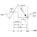
- FIG. 4 is a diagram illustrating an example of a sampling timing determination method.
- FIG. 4 shows levels according to the carrier signal and the duties (duty 0, duty 1, duty 2, duty 3) calculated by the current control unit 506 and the duty correction unit 512.
- switching element Q22 will be described as an example (although it will be described at the time of regeneration in FIG. 3B), but switching element Q24 (at the time of powering in FIG. 3A) may be the same. Incidentally, when both arms are driven, the same may be applied to any one of the switching elements Q22, Q24.
- the switching element Q22 is turned off, and the off period starts.
- the duty is changed (set) from duty 1 to duty 2 in response to the occurrence of a carrier signal peak.
- the switching element Q22 is turned on, and the off period from time t1 ends (the on period begins).
- the duty is changed (set) from duty 2 to duty 3 in response to the occurrence of a trough in the carrier signal.
- the sampling timing is determined so that the average value of the reactor current IL during the on / off period is sampled as described above. Specifically, the sampling timing is set at an intermediate point in the on / off period. In the example shown in FIG. 4, the intermediate time point of the off period in the current off period (the period from time t0 to time t3) is time t2. In FIG. 4, the positions corresponding to the sampling timing on the carrier signal are indicated by white circles.
- the sampling timing is The time “(a + b) / 2” has elapsed since the start of the off period (time t0).
- the intermediate time point in the ON / OFF period may be an intermediate time point based on the inversion timing of the gate signals of the switching elements Q22 and Q24, or a strict intermediate time point based on the conduction state of the switching elements Q22 and Q24. Also good.
- the sampling timing may be offset back and forth with respect to the intermediate point in the on / off period.
- the sampling timing may be set to a time point after a predetermined delay time ⁇ with respect to the intermediate time point in the on / off period.
- the positions corresponding to the sampling timing with the predetermined delay time ⁇ added are indicated by black circles on the carrier signal.
- the predetermined delay time ⁇ may correspond to a delay time generated in the filter 502. That is, since the detection signal of the current sensor is passed through the filter 502, a delay time is generated. Therefore, the sampling timing may be delayed by a predetermined delay time ⁇ so that the influence of the delay time is compensated. .
- FIG. 5 is a diagram illustrating the relationship between each sampling timing and the duty set based on the sampling value of the reactor current IL acquired at each sampling timing.
- FIG. 5 shows the sampling timings P1, P2, and P3.
- the duty calculated based on the sampling value of the reactor current IL acquired at the sampling timing P1 in the off period OFF1 is from the middle of the next on period ON1 (carrier signal valley) as shown by the arrow in the figure. It is set as duty2.
- the duty2 is maintained until the next off period OFF2 (the peak of the carrier signal).
- the duty calculated based on the sampling value of the reactor current IL acquired at the sampling timing P2 in the ON period ON1 is the middle of the next OFF period OFF2 (the peak of the carrier signal) as shown by the arrow in the figure. )
- the duty3 is maintained until the next ON period ON2 (the trough of the carrier signal).
- the duty calculated based on the sampling value of the reactor current IL acquired at the sampling timing P3 in the off period OFF2 is the middle of the next on period ON2 (carrier signal valley) as shown by an arrow in the figure. ) To duty4.
- the sampling value of reactor current IL sampled in each on / off period is used to calculate the duty set from the peak / valley of the carrier signal in the next off / on period.
- FIG. 6 is a flowchart showing an example of a duty correction method in the duty correction unit 512. 6 may be realized in cooperation with the sampling timing calculation unit 516.
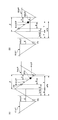
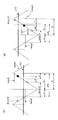
- FIG. 7 is an explanatory diagram of FIG. 6 and is a schematic diagram in which a part of FIG. 5 is extracted. Here, the correction of duty 3 will be described.
- FIG. 7A shows the duty 3 before correction (duty calculated by the current control unit 506)
- FIG. 7B shows the duty 3 after correction (duty correction unit). (Duty corrected by 512).
- the time ⁇ corresponds to the time required for processing from the sampling timing P3 to the final setting of duty 4, and hereinafter, “duty setting required time ⁇ ”. That's it.
- the duty setting required time ⁇ occupies most of the duty calculation processing time required from the sampling timing P3 to the final calculation of duty4 by the duty correction unit 512.
- the duty 3 before correction is calculated based on the sampling value of the reactor current IL acquired at the sampling timing P2, as described above.
- the current control unit 506 calculates the duty 3 before correction based on the reactor current IL acquired at the sampling timing P2 and the target value IL * of the reactor current IL from the voltage control unit 508.
- the process shown in FIG. 6 is executed at or after the time when the duty before correction (duty 3 before correction in this example) is calculated by the current control unit 506, and this duty setting timing (in this example, the carrier signal) It is executed to complete until the next mountain).
- this duty setting timing in this example, the carrier signal
- the process shown in FIG. 6 is described in a mode realized by software. However, as described above, part or all of the process shown in FIG. 6 may be realized by hardware or the like. Good.
- the most recent sampling timing P3 is calculated based on the duty 3 before correction calculated by the current control unit 506, the currently set duty 2, and the current carrier signal frequency. Specifically, “a” (see FIG. 7A, etc.) is calculated based on the currently set duty 2 and the current carrier signal frequency, and before the correction calculated by the current control unit 506. “B” (see FIG. 7A, etc.) is calculated based on the current duty 3 and the frequency of the current carrier signal (or the frequency of the carrier signal after the change if it changes from the next peak). (A + b) / 2 ′′ (see FIG. 7A and the like) is calculated (see white circle P3 in FIG. 7). As described above, when the delay time is considered, the sampling timing may be calculated as “(a + b) / 2 + ⁇ ” (see the black circle P3 in FIG. 7).
- step 604 it is determined whether the time from the latest sampling timing P3 to the next duty setting timing (next trough of the carrier signal) is equal to or longer than the duty setting required time ⁇ .
- the sampling timing is determined as “(a + b) / 2” (see the white circle P3 in FIG. 7)
- Formula (1) Note that ⁇ (a + b) / 2 ⁇ a ⁇ represents the time from the peak of the carrier signal to the latest sampling timing P3, and ⁇ represents the time from the peak of the carrier signal to the valley.
- ⁇ changes according to the frequency of the carrier signal, it may be varied according to the current carrier signal frequency (or the changed carrier signal frequency when changing from the next peak).
- the sampling timing is determined as “(a + b) / 2 + ⁇ ” (see the black circle P3 in FIG. 7)
- step 604 if the time from the latest sampling timing P3 to the next duty setting timing is equal to or longer than the duty setting required time ⁇ , the processing ends. That is, in this case, it is determined that the correction of the duty 3 before the correction is unnecessary, and the process ends without performing the correction of the duty 3 before the correction.
- the duty 3 before correction is set as it is at the next duty setting timing (next trough of the carrier signal).
- the process proceeds to step 606.
- step 606 the duty 3 before correction is corrected. That is, the duty 3 before correction is corrected so that the time from the latest sampling timing P3 to the next duty setting timing is equal to or longer than the duty setting required time ⁇ .
- the sampling timing is determined as “(a + b) / 2” (see the white circle P3 in FIG. 7) (see the white circle P3 in FIG. 7)
- the duty corresponding to the maximum value of “b” that satisfies the relationship of the above equation (1) is corrected. You may determine as duty3 after.
- the sampling timing is determined as “(a + b) / 2 + ⁇ ” (see black circle P3 in FIG. 7)
- the duty corresponding to the maximum value of “b” that satisfies the relationship of the above equation (2) is corrected. You may determine as duty3 after.
- the next duty setting timing (carrier) from the latest sampling timing P3 (see black circle P3 in FIG. 7). Since the time until the next valley of the signal is shorter than the duty setting required time ⁇ , the process proceeds to step 606, where the duty 3 before correction is corrected. As a result of this correction, as shown in FIG. 7B, the time from the latest sampling timing P3 (see black circle P3 in FIG. 7) to the next duty setting timing (next trough of the carrier signal) is set to the duty setting. The required time is ⁇ or more.
- the duty set in the current duty setting cycle is finally determined so that the time until the duty setting timing is equal to or longer than the duty setting required time ⁇ .
- the duty (duty 4 in this example) calculated based on the sampling value of the reactor current IL sampled at the latest sampling timing P3, and the duty set in the next duty setting timing (duty 4 in this example) Can be completed (to be settable) by the next duty setting timing.
- the duty correction method set when the carrier signal becomes a peak has been described, but the duty correction method set when the carrier signal becomes a valley is the same. Good.
- the same applies to the duty (duty 4) calculated based on the sampling value of the reactor current IL sampled at the sampling timing P3.
- the duty correction may be performed in consideration of the upper limit value or the lower limit value of the duty. Good.
- FIG. 8 is an explanatory diagram of a duty correction method considering the lower limit value ⁇ 1 of the duty with respect to the duty set when the carrier signal becomes a peak.
- the duty corresponding to the maximum value of “b” that satisfies the relationship of the above formula (1) or (2) is referred to as “critical point duty”.
- FIG. 8A shows a case where the lower limit value ⁇ 1 of the duty is larger than the critical point duty
- FIG. 8B shows a case where the lower limit value ⁇ 1 of the duty is smaller than the critical point duty.
- the lower limit value ⁇ 1 of the duty is a physical limit value necessary for preventing a short circuit, and may be changed according to the dead time, the frequency of the carrier signal, or the like.
- the duty when the lower limit value ⁇ 1 of the duty is larger than the critical point duty, the duty may be corrected so as to be equal to or higher than the lower limit value ⁇ 1 of the duty.
- the lower limit value ⁇ 1 of the duty when the lower limit value ⁇ 1 of the duty is smaller than the critical point duty, the duty may be corrected so as to be equal to or higher than the critical point duty.
- FIG. 9 is an explanatory diagram of a duty correction method considering the upper limit value ⁇ 2 of the duty with respect to the duty set when the carrier signal becomes a valley.
- FIG. 9A shows a case where the upper limit value ⁇ 2 of the duty is smaller than the critical point duty
- FIG. 9B shows a case where the upper limit value ⁇ 2 of the duty is larger than the critical point duty.
- the upper limit value ⁇ 2 of the duty is a physical limit value necessary for preventing a short circuit, and may change according to the dead time, the frequency of the carrier signal, and the like.
- the duty when the upper limit value ⁇ 2 of the duty is smaller than the critical point duty, the duty may be corrected so as to be equal to or lower than the upper limit value ⁇ 2 of the duty.
- the duty when the upper limit value ⁇ 2 of the duty is larger than the critical point duty, the duty may be corrected so as to be equal to or lower than the critical point duty.
- the time from the most recent sampling timing P3 to the next duty setting timing is less than the duty setting required time ⁇
- the duty (critical point duty) corresponding to the maximum value of “b” that satisfies the relationship of the above formula (1) or (2) is set so as to be the duty setting required time ⁇ .
- a duty different from the critical point duty may be set so that the time from the timing P3 to the next duty setting timing becomes longer than the duty setting required time ⁇ . For example, when correcting the duty set when the carrier signal becomes a peak, the duty may be corrected to a duty slightly larger than the critical point duty. Further, when correcting the duty set when the carrier signal becomes a valley, it may be corrected to a duty slightly smaller than the critical point duty.
- the duty is set for each peak (peak and valley) of the carrier signal.
- the duty may be set for each timing shifted by a predetermined phase from the peak of the carrier signal.
- the DC / DC converter 20 is a bidirectional DC / DC converter, but the type of the converter is arbitrary.
- the DC / DC converter 20 may be a converter that can only step up or can only step down.
- the upper arm may be configured to have only the diode D22 without the switching element 22.
- the lower arm may be configured to have only the diode D24 without the switching element 24.
- the final duty is determined by correcting the duty calculated by the current control unit 506 by the duty correction unit 512, but the current control unit 506 is a function of the duty correction unit 512. May be included.
- the current control unit 506 sets the critical point duty as the upper limit value or the lower limit value, based on the sampling value of the reactor current IL from the ADC 504 and the target value IL * of the reactor current IL from the voltage control unit 508, The duty may be determined.
- the DC / DC converter 20 is used for a vehicle, but may be used for other purposes (for example, a power supply device of another electric device). Further, the DC / DC converter 20 may be used for other purposes (for example, for an electric steering device) for a vehicle.
Landscapes
- Engineering & Computer Science (AREA)
- Power Engineering (AREA)
- Dc-Dc Converters (AREA)
Abstract
Description
キャリア信号の半周期に対応した所定のデューティ設定周期毎にデューティを設定し、設定したデューティと前記キャリア信号との関係に応じた切換タイミングで、前記コンバータのスイッチング素子のオン/オフ切換を実行する制御装置とを備え、
前記制御装置は、次回のデューティ設定タイミングまでに、前記リアクトルを流れる電流値をサンプリングし且つ前記サンプリングした電流値に基づいて次回のデューティ設定タイミングで設定するデューティを演算することを、完了するように、今回のデューティ設定周期で設定するデューティを決定することを特徴とする、コンバータ装置が提供される。
Transistor)である。尚、スイッチング素子Q22,Q24は、ダイオード(例えばフリーホイールダイオード)D22,24を外付け素子と用いる通常のIGBTであってもよいし、ダイオードD22,24を内蔵した逆導通IGBT(RC(Reverse Conducting)-IGBT)であってもよい。いずれの場合も、上アームのスイッチング素子Q22のコレクタはインバータ30の正極ラインに接続されており、上アームのスイッチング素子Q22のエミッタは下アームのスイッチング素子Q24のコレクタに接続されている。また、下アームのスイッチング素子Q24のエミッタは、インバータ30の負極ライン及びバッテリ10の負極に接続されている。尚、スイッチング素子Q22、Q24は、MOSFET(Metal Oxide Semiconductor Field-Effect Transistor)のような、IGBT以外の他のスイッチング素子であってもよい。
integrated circuit)やFPGA(Field Programmable Gate Array)により実現されてもよい。また、半導体駆動装置50の各種機能は、複数のECUにより協動して実現されてもよい。
β-{(a+b)/2-a}≧γ 式(1)
尚、{(a+b)/2-a}は、キャリア信号の山から直近のサンプリングタイミングP3までの時間を表し、βは、キャリア信号の山から谷までの時間を表す。βは、キャリア信号の周波数に応じて変化するため、現在のキャリア信号の周波数(又は次の山から変化する場合は変化後のキャリア信号の周波数)に応じて可変されてもよい。
尚、サンプリングタイミングが“(a+b)/2+α”として決定される場合(図7中の黒丸P3参照)、次の関係式が満たされるか否かが判定される。
β-{(a+b)/2-a+α}≧γ 式(2)
本ステップ604において、直近のサンプリングタイミングP3から次回のデューティ設定タイミングまでの時間が、duty設定必要時間γ以上である場合は、そのまま終了する。即ち、この場合、補正前のduty3の補正が不要であると判断して、補正前のduty3の補正を行うことなく終了する。この場合、デューティは、補正前のduty3がそのまま次回のデューティ設定タイミング(キャリア信号の次の谷)で設定されることになる。他方、直近のサンプリングタイミングP3から次回のデューティ設定タイミングまでの時間が、duty設定必要時間γ以上でない場合は、ステップ606に進む。
10 バッテリ
20 DC/DCコンバータ
30 インバータ
40 走行用モータ
50 半導体駆動装置
Q1,Q2 U相に係るスイッチング素子
Q3,Q4 V相に係るスイッチング素子
Q5,Q6 W相に係るスイッチング素子
Q22 上アームのスイッチング素子
Q24 下アームのスイッチング素子
502 フィルタ
504 ADC
506 電流制御部
508 電圧制御部
510 モータ目標電圧算出部
512 デューティ補正部
513 キャリア生成部
514 ゲート信号生成部
516 サンプリングタイミング算出部
540 モータ制御部
560 走行制御部
Claims (6)
- スイッチング素子及びリアクトルを有するコンバータと、
キャリア信号の半周期に対応した所定のデューティ設定周期毎にデューティを設定し、設定したデューティと前記キャリア信号との関係に応じた切換タイミングで、前記コンバータのスイッチング素子のオン/オフ切換を実行する制御装置とを備え、
前記制御装置は、次回のデューティ設定タイミングまでに、前記リアクトルを流れる電流値をサンプリングし且つ前記サンプリングした電流値に基づいて次回のデューティ設定タイミングで設定するデューティを演算することを、完了するように、今回のデューティ設定周期で設定するデューティを決定することを特徴とする、コンバータ装置。 - 前記制御装置は、前記リアクトルを流れる電流値をサンプリングするサンプリングタイミングから次回のデューティ設定タイミングまでの時間が所定時間以上になるように、今回のデューティ設定周期で設定するデューティを決定する、請求項1に記載のコンバータ装置。
- 前記リアクトルを流れる電流値をサンプリングするサンプリングタイミングは、前記スイッチング素子の1回のオン期間又はオフ期間における前記リアクトルを流れる電流の平均値がサンプルされるように決定される、請求項1又は2に記載のコンバータ装置。
- 前記リアクトルを流れる電流値をサンプリングするサンプリングタイミングは、前回のデューティ設定周期で設定したデューティと、今回のデューティ設定周期で設定するデューティとに基づいて決定される、請求項1~3のうちのいずれか1項に記載のコンバータ装置。
- 前記リアクトルを流れる電流値をサンプリングするサンプリングタイミングは、前回のデューティ設定周期で設定したデューティに応じた前回の切換タイミングと、今回のデューティ設定周期で設定するデューティに応じた今回の切換タイミングとの間の中間時点に対応する、請求項4に記載のコンバータ装置。
- 前記リアクトルを流れる電流値をサンプリングするサンプリングタイミングは、前回のデューティ設定周期で設定したデューティに応じた前回の切換タイミングと、今回のデューティ設定周期で設定するデューティに応じた今回の切換タイミングとの間の中間時点に対して所定の遅延時間後に対応する、請求項4に記載のコンバータ装置。
Priority Applications (3)
| Application Number | Priority Date | Filing Date | Title |
|---|---|---|---|
| DE112013005939.8T DE112013005939T5 (de) | 2012-12-12 | 2013-11-07 | Wandlergerät |
| US14/441,953 US20150318793A1 (en) | 2012-12-12 | 2013-11-07 | Converter apparatus |
| CN201380065372.6A CN104885350A (zh) | 2012-12-12 | 2013-11-07 | 转换器装置 |
Applications Claiming Priority (2)
| Application Number | Priority Date | Filing Date | Title |
|---|---|---|---|
| JP2012271390A JP5617909B2 (ja) | 2012-12-12 | 2012-12-12 | コンバータ装置 |
| JP2012-271390 | 2012-12-12 |
Publications (1)
| Publication Number | Publication Date |
|---|---|
| WO2014091843A1 true WO2014091843A1 (ja) | 2014-06-19 |
Family
ID=50934141
Family Applications (1)
| Application Number | Title | Priority Date | Filing Date |
|---|---|---|---|
| PCT/JP2013/080162 Ceased WO2014091843A1 (ja) | 2012-12-12 | 2013-11-07 | コンバータ装置 |
Country Status (5)
| Country | Link |
|---|---|
| US (1) | US20150318793A1 (ja) |
| JP (1) | JP5617909B2 (ja) |
| CN (1) | CN104885350A (ja) |
| DE (1) | DE112013005939T5 (ja) |
| WO (1) | WO2014091843A1 (ja) |
Families Citing this family (8)
| Publication number | Priority date | Publication date | Assignee | Title |
|---|---|---|---|---|
| JP6458684B2 (ja) * | 2015-08-28 | 2019-01-30 | 日産自動車株式会社 | 電力制御方法、及び、電力制御装置 |
| DE102016205300B4 (de) | 2016-03-31 | 2019-08-08 | Wago Verwaltungsgesellschaft Mbh | Stromregelung eines pulsweitenmodulierten Stromrichters |
| DE102016014093A1 (de) | 2016-07-01 | 2018-01-04 | Sew-Eurodrive Gmbh & Co Kg | Verfahren zum Betreiben eines Antriebs mit Wechselrichter, insbesondere eines Umrichters und Antrieb mit Wechselrichter |
| EP3270497B1 (en) * | 2016-07-14 | 2018-12-12 | Nxp B.V. | A controller for a power converter |
| JP6702852B2 (ja) * | 2016-12-26 | 2020-06-03 | 株式会社ケーヒン | パワーコントロールユニット |
| KR102686893B1 (ko) * | 2017-02-15 | 2024-07-19 | 에이치엘만도 주식회사 | 전동식 조향 장치의 모터 제어 장치 및 모터 제어 방법 |
| JP7230735B2 (ja) * | 2018-08-10 | 2023-03-01 | 株式会社デンソー | 車両用電力変換装置 |
| CN114362495B (zh) * | 2022-01-28 | 2025-12-30 | 北京小米移动软件有限公司 | 电路保护方法、装置、电器设备及存储介质 |
Citations (2)
| Publication number | Priority date | Publication date | Assignee | Title |
|---|---|---|---|---|
| JP2009100607A (ja) * | 2007-10-19 | 2009-05-07 | Hitachi Computer Peripherals Co Ltd | デジタル制御電源装置 |
| JP2011091981A (ja) * | 2009-10-26 | 2011-05-06 | Hitachi Computer Peripherals Co Ltd | 力率改善装置及びその制御方法 |
Family Cites Families (5)
| Publication number | Priority date | Publication date | Assignee | Title |
|---|---|---|---|---|
| US6404655B1 (en) * | 1999-12-07 | 2002-06-11 | Semikron, Inc. | Transformerless 3 phase power inverter |
| JP2008035609A (ja) * | 2006-07-28 | 2008-02-14 | Sharp Corp | スイッチング電源回路 |
| US9379643B2 (en) * | 2010-12-23 | 2016-06-28 | The Regents Of The University Of Colorado, A Body Corporate | Electrosurgical generator controller for regulation of electrosurgical generator output power |
| JP2012161222A (ja) * | 2011-02-03 | 2012-08-23 | Meidensha Corp | 並列多重チョッパ装置 |
| US9270202B2 (en) * | 2013-03-11 | 2016-02-23 | Covidien Lp | Constant power inverter with crest factor control |
-
2012
- 2012-12-12 JP JP2012271390A patent/JP5617909B2/ja active Active
-
2013
- 2013-11-07 CN CN201380065372.6A patent/CN104885350A/zh active Pending
- 2013-11-07 US US14/441,953 patent/US20150318793A1/en not_active Abandoned
- 2013-11-07 WO PCT/JP2013/080162 patent/WO2014091843A1/ja not_active Ceased
- 2013-11-07 DE DE112013005939.8T patent/DE112013005939T5/de not_active Withdrawn
Patent Citations (2)
| Publication number | Priority date | Publication date | Assignee | Title |
|---|---|---|---|---|
| JP2009100607A (ja) * | 2007-10-19 | 2009-05-07 | Hitachi Computer Peripherals Co Ltd | デジタル制御電源装置 |
| JP2011091981A (ja) * | 2009-10-26 | 2011-05-06 | Hitachi Computer Peripherals Co Ltd | 力率改善装置及びその制御方法 |
Also Published As
| Publication number | Publication date |
|---|---|
| JP5617909B2 (ja) | 2014-11-05 |
| JP2014117122A (ja) | 2014-06-26 |
| US20150318793A1 (en) | 2015-11-05 |
| DE112013005939T5 (de) | 2015-09-10 |
| CN104885350A (zh) | 2015-09-02 |
Similar Documents
| Publication | Publication Date | Title |
|---|---|---|
| JP5617909B2 (ja) | コンバータ装置 | |
| JP6040800B2 (ja) | コンバータ装置 | |
| JP5737309B2 (ja) | 電力変換装置 | |
| US10027262B2 (en) | Pseudorandom PWM variation based on motor operating point | |
| JP6233178B2 (ja) | 昇圧コンバータ装置 | |
| US9866156B2 (en) | Motor control device and motor control method | |
| JP6089978B2 (ja) | スイッチトリラクタンスモータのpam駆動装置 | |
| WO2008007723A1 (en) | Load drive device and vehicle using the same | |
| CN105896967B (zh) | 升压控制装置以及升压控制方法 | |
| JPWO2010137128A1 (ja) | コンバータの制御装置およびそれを備える電動車両 | |
| CN105896968B (zh) | 升压控制装置 | |
| CN109687696B (zh) | 电源系统 | |
| JP6040787B2 (ja) | 電力変換装置 | |
| US9960726B1 (en) | Electric drive power converter with low distortion dead-time insertion | |
| JP2011223701A (ja) | コンバータの電圧推定装置および電圧推定方法 | |
| US9543877B2 (en) | Control apparatus for a switched reluctance motor | |
| US11689133B1 (en) | Inverter switching frequency control systems and methods | |
| JP2011223674A (ja) | コンバータの制御装置およびそれを備える電動車両 | |
| JP5991212B2 (ja) | 電力変換装置 | |
| JP5987777B2 (ja) | 電力変換装置 | |
| JP2011182515A (ja) | 電動機駆動システムおよびそれを備える電動車両 | |
| JP2011155787A (ja) | 回転電機制御システム | |
| JP2010220306A (ja) | モータの制御装置 | |
| JP2014138537A (ja) | 電力変換装置 | |
| JP7716890B2 (ja) | 昇圧制御装置及び昇圧装置 |
Legal Events
| Date | Code | Title | Description |
|---|---|---|---|
| 121 | Ep: the epo has been informed by wipo that ep was designated in this application |
Ref document number: 13861729 Country of ref document: EP Kind code of ref document: A1 |
|
| WWE | Wipo information: entry into national phase |
Ref document number: 14441953 Country of ref document: US |
|
| WWE | Wipo information: entry into national phase |
Ref document number: 1120130059398 Country of ref document: DE Ref document number: 112013005939 Country of ref document: DE |
|
| 122 | Ep: pct application non-entry in european phase |
Ref document number: 13861729 Country of ref document: EP Kind code of ref document: A1 |