WO2014087840A1 - 動き検出用固体撮像装置及び動き検出システム - Google Patents
動き検出用固体撮像装置及び動き検出システム Download PDFInfo
- Publication number
- WO2014087840A1 WO2014087840A1 PCT/JP2013/081220 JP2013081220W WO2014087840A1 WO 2014087840 A1 WO2014087840 A1 WO 2014087840A1 JP 2013081220 W JP2013081220 W JP 2013081220W WO 2014087840 A1 WO2014087840 A1 WO 2014087840A1
- Authority
- WO
- WIPO (PCT)
- Prior art keywords
- pixel
- motion detection
- signal
- pixels
- motion
- Prior art date
- Legal status (The legal status is an assumption and is not a legal conclusion. Google has not performed a legal analysis and makes no representation as to the accuracy of the status listed.)
- Ceased
Links
Images


Classifications
-
- H—ELECTRICITY
- H04—ELECTRIC COMMUNICATION TECHNIQUE
- H04N—PICTORIAL COMMUNICATION, e.g. TELEVISION
- H04N23/00—Cameras or camera modules comprising electronic image sensors; Control thereof
- H04N23/60—Control of cameras or camera modules
- H04N23/68—Control of cameras or camera modules for stable pick-up of the scene, e.g. compensating for camera body vibrations
- H04N23/681—Motion detection
- H04N23/6811—Motion detection based on the image signal
-
- H—ELECTRICITY
- H04—ELECTRIC COMMUNICATION TECHNIQUE
- H04N—PICTORIAL COMMUNICATION, e.g. TELEVISION
- H04N25/00—Circuitry of solid-state image sensors [SSIS]; Control thereof
- H04N25/10—Circuitry of solid-state image sensors [SSIS]; Control thereof for transforming different wavelengths into image signals
- H04N25/11—Arrangement of colour filter arrays [CFA]; Filter mosaics
- H04N25/13—Arrangement of colour filter arrays [CFA]; Filter mosaics characterised by the spectral characteristics of the filter elements
- H04N25/134—Arrangement of colour filter arrays [CFA]; Filter mosaics characterised by the spectral characteristics of the filter elements based on three different wavelength filter elements
-
- H—ELECTRICITY
- H04—ELECTRIC COMMUNICATION TECHNIQUE
- H04N—PICTORIAL COMMUNICATION, e.g. TELEVISION
- H04N25/00—Circuitry of solid-state image sensors [SSIS]; Control thereof
- H04N25/50—Control of the SSIS exposure
- H04N25/53—Control of the integration time
- H04N25/533—Control of the integration time by using differing integration times for different sensor regions
-
- H—ELECTRICITY
- H04—ELECTRIC COMMUNICATION TECHNIQUE
- H04N—PICTORIAL COMMUNICATION, e.g. TELEVISION
- H04N25/00—Circuitry of solid-state image sensors [SSIS]; Control thereof
- H04N25/50—Control of the SSIS exposure
- H04N25/57—Control of the dynamic range
- H04N25/58—Control of the dynamic range involving two or more exposures
- H04N25/581—Control of the dynamic range involving two or more exposures acquired simultaneously
- H04N25/583—Control of the dynamic range involving two or more exposures acquired simultaneously with different integration times
-
- H—ELECTRICITY
- H04—ELECTRIC COMMUNICATION TECHNIQUE
- H04N—PICTORIAL COMMUNICATION, e.g. TELEVISION
- H04N25/00—Circuitry of solid-state image sensors [SSIS]; Control thereof
- H04N25/70—SSIS architectures; Circuits associated therewith
-
- H—ELECTRICITY
- H04—ELECTRIC COMMUNICATION TECHNIQUE
- H04N—PICTORIAL COMMUNICATION, e.g. TELEVISION
- H04N25/00—Circuitry of solid-state image sensors [SSIS]; Control thereof
- H04N25/70—SSIS architectures; Circuits associated therewith
- H04N25/703—SSIS architectures incorporating pixels for producing signals other than image signals
- H04N25/704—Pixels specially adapted for focusing, e.g. phase difference pixel sets
-
- H—ELECTRICITY
- H04—ELECTRIC COMMUNICATION TECHNIQUE
- H04N—PICTORIAL COMMUNICATION, e.g. TELEVISION
- H04N25/00—Circuitry of solid-state image sensors [SSIS]; Control thereof
- H04N25/70—SSIS architectures; Circuits associated therewith
- H04N25/76—Addressed sensors, e.g. MOS or CMOS sensors
- H04N25/78—Readout circuits for addressed sensors, e.g. output amplifiers or A/D converters
-
- H—ELECTRICITY
- H10—SEMICONDUCTOR DEVICES; ELECTRIC SOLID-STATE DEVICES NOT OTHERWISE PROVIDED FOR
- H10F—INORGANIC SEMICONDUCTOR DEVICES SENSITIVE TO INFRARED RADIATION, LIGHT, ELECTROMAGNETIC RADIATION OF SHORTER WAVELENGTH OR CORPUSCULAR RADIATION
- H10F39/00—Integrated devices, or assemblies of multiple devices, comprising at least one element covered by group H10F30/00, e.g. radiation detectors comprising photodiode arrays
- H10F39/80—Constructional details of image sensors
- H10F39/813—Electronic components shared by multiple pixels, e.g. one amplifier shared by two pixels
-
- H—ELECTRICITY
- H04—ELECTRIC COMMUNICATION TECHNIQUE
- H04N—PICTORIAL COMMUNICATION, e.g. TELEVISION
- H04N25/00—Circuitry of solid-state image sensors [SSIS]; Control thereof
- H04N25/70—SSIS architectures; Circuits associated therewith
- H04N25/76—Addressed sensors, e.g. MOS or CMOS sensors
- H04N25/77—Pixel circuitry, e.g. memories, A/D converters, pixel amplifiers, shared circuits or shared components
- H04N25/778—Pixel circuitry, e.g. memories, A/D converters, pixel amplifiers, shared circuits or shared components comprising amplifiers shared between a plurality of pixels, i.e. at least one part of the amplifier must be on the sensor array itself
Definitions
- the present invention relates to a solid-state imaging device for motion detection that detects a motion of an object on an imaging screen, and a motion detection system.
- CMOS sensor types for mobile phone cameras have been rapidly increasing in recent years.
- Each pixel cell of the CMOS sensor type solid-state imaging device has a photoelectric conversion unit (hereinafter referred to as a pixel) that generates a signal charge corresponding to incident light, and an amplification that converts the signal charge of the photoelectric conversion unit into a signal voltage and amplifies it.
- a photoelectric conversion unit hereinafter referred to as a pixel
- the solid-state imaging device may not only capture an object (subject) but also detect the movement of the object on the imaging screen of the solid-state imaging device. For example, the same field of view is continuously imaged, and it is detected that a person has entered the field of view, and various devices are controlled in response to the person's intrusion, or the intrusion of this person is notified. Record.
- the apparatus Since the former method 1 requires a frame memory, the apparatus becomes larger due to an increase in power consumption and an increase in circuit scale. In addition, costs will increase.
- the first and second pixels that are spatially adjacent to each other are treated as one set, and these pixel sets are treated as one sensing unit.
- the photoelectric conversion time of the second pixel is set as the photoelectric conversion time of the first pixel.
- the conversion time is doubled, and the motion of the object on the imaging screen is detected based on the difference between the signal of the first pixel and the signal of 1/2 of the second pixel.
- Method 2 can perform motion detection without requiring a frame memory.
- the difference does not become 0 for a normal stationary object as described above. This is because the difference signal does not become 0 because the signal amount of the two pixels in the pair is different at the end of the photographed object, and the object is erroneously recognized as moving.
- the difference signal does not become 0 because the signal amount of the two pixels in the pair is different at the end of the photographed object, and the object is erroneously recognized as moving.
- the Bayer method which is a typical color filter arrangement
- the present invention is a solid-state imaging device for motion detection that detects the motion of an object on an imaging screen, and provides a pixel configuration and a calculation system that suppress an error signal (noise signal) generated in the contour of a subject. Accordingly, it is an object of the present invention to provide a motion detection solid-state imaging device that not only simplifies subsequent signal processing but also improves the motion detection capability of a moving object.
- the solid-state imaging device for motion detection includes two 2 ⁇ 2 pixels arranged in the vertical and horizontal directions as one set, and two adjacent pixels in the diagonal direction as one set, and an oblique direction perpendicular thereto. The remaining two pixels are set as one set, and the photoelectric conversion time between the two sets is changed. Next, the output signal amount of the set on one side is adjusted by the ratio of the two photoelectric conversion times, and the difference between the two is detected to detect the motion, and the contour of the subject is averaged. Suppresses generated noise. Further, the adjustment of the signal amount due to the difference in photoelectric conversion time may be performed by adjusting the pixel size of each of the two sets.
- the present invention it is possible to provide a solid-state imaging device that suppresses the generation of noise at the contour and performs motion detection. Since noise at the contour can be suppressed, the detection capability of a moving object can be improved, and a motion detection imaging system with low power consumption can be provided.
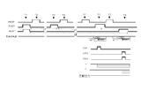
- FIG. 3 is a diagram for explaining a cell layout, a motion detection circuit configuration and a driving method according to the present invention.
- FIG. 6 is a diagram illustrating a photoelectric conversion time change of an output level of a pair of pixels. These are diagrams explaining the driving method of the present invention, and are diagrams showing timing charts generated in each signal line and pulse line. These are the figures explaining the circuit structure for obtaining a normal captured image, performing the motion detection of this invention. These are figures explaining another motion detection circuit configuration and driving method of the present invention.
- FIG. 6 is a diagram illustrating a photoelectric conversion time change of an output level of a pair of pixels.
- FIG. 8 is a diagram for explaining a driving method, and is a diagram illustrating a timing chart generated in each signal line and pulse line.
- FIG. 4 is a specific pixel cell configuration of the present invention, and is a diagram showing the positional relationship of the pattern edge with respect to the pixel when the pattern edge position moves in the vertical direction of the pixel arrangement from the vertical pixel gap. is there.
- FIG. 5 is a diagram showing a signal output pattern generated in a pixel and a motion detection signal pattern after the pixel signal processing of the present invention at the timing shown in FIG. Is a specific pixel cell configuration of the present invention, and in the three cases where the pattern edge position and the pixel are displaced in the vertical direction while the pattern edge position exists in the vertical pixel gap.
- FIG. 6 is a diagram showing a signal output pattern generated in a pixel and a motion detection signal pattern after undergoing the pixel signal processing of the present invention in the case of the positional relationship shown in FIG.
- FIG. 6 is a diagram showing a signal output pattern generated in a pixel and a motion detection signal pattern after undergoing the pixel signal processing of the present invention in the case of the positional relationship shown in FIG.
- FIG. 8 is a diagram showing a signal output pattern generated in a pixel and a motion detection signal pattern after the pixel signal processing of the present invention at the timing shown in FIG. Is a configuration of a pixel cell in which the specific color filter of the present invention is arranged, and the positional relationship between the pattern end and the pixel is shifted in the vertical direction in a state where the position of the pattern end exists in the center of the pixel in the vertical direction. It is the figure which shows the positional relationship in three cases.
- FIG. 9 is a diagram showing a signal output pattern generated in a pixel and a motion detection signal pattern after the pixel signal processing according to the present invention in the case of the positional relationship shown in FIG.
- FIG. 10 is a diagram showing a specific cell configuration of a 4-pixel 1-cell in the embodiment of FIG. 9; These are still another embodiments of the present invention, and are a diagram illustrating a configuration of a 4-pixel 1 cell sharing an output circuit and a configuration of an output circuit at the end of a vertical signal line.
- FIG. 4 is a diagram for explaining a driving method, and is a diagram showing a photoelectric conversion time change of an output level of a pair of pixels. These are diagrams explaining the driving method of the present invention, and are diagrams showing timing charts generated in each signal line and pulse line.
- FIG. 10 is a diagram showing a specific cell configuration of a 4-pixel 1-cell in the embodiment of FIG. 9; These are still another embodiments of the present invention, and are a diagram illustrating a configuration of a 4-pixel 1 cell sharing an output circuit and a configuration of an output circuit at the end of a vertical signal line.
- FIG. 4 is a diagram for explaining a driving method, and is a diagram showing a photoelectric conversion
- FIG. 5 is still another embodiment of the present invention, and is a diagram showing a configuration diagram of a 4-pixel 1-cell in which the size of a pixel in a cell is changed and sensitivity is changed, and a configuration of an output circuit at the end of a vertical signal line.
- FIG. 4 is a diagram for explaining a driving method, and is a diagram showing a photoelectric conversion time change of an output level of a pair of pixels. These are diagrams explaining the driving method of the present invention, and are diagrams showing timing charts generated in each signal line and pulse line.
- FIG. 13 is a diagram showing a repetitive cell arrangement of pixels and output circuits when color filters are arranged in the cell having the configuration shown in FIG. FIG.
- FIG. 13 is a diagram showing an embodiment in which pixels and output cell repetitive cells are arranged efficiently when the color filter is arranged in the cell having the configuration shown in FIG. Is a specific pixel cell configuration of the present invention, and is a configuration diagram of a 4-pixel 1-cell in which the size of the pixel in the cell is changed and the sensitivity is changed, corresponding to FIG. It is a figure which shows the positional relationship of the pattern edge part with respect to a pixel in three timings shown in below-mentioned FIG.15 (b) at the time of moving to.
- FIG. 4 is a diagram for explaining a driving method, and is a diagram showing a photoelectric conversion time change of an output level of a pair of pixels.
- FIG. 4 is a diagram for explaining a driving method, and is a diagram showing a photoelectric conversion time change of an output level of a pair of pixels.
- FIGS. 15B and 15C are diagram showing a signal output pattern generated in a pixel at two timings shown in FIGS. 15B and 15C and a motion detection signal pattern after the pixel signal processing of the present invention. is there.
- figures which show the whole structure of the motion detection system to which this invention is applied are the whole block diagrams which show the modification of the motion detection system to which this invention is applied.
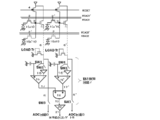
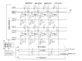
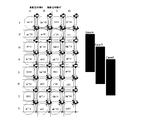
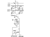
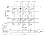
- FIG. 1 is a diagram showing the overall configuration of a solid-state imaging device for motion detection according to the present invention.
- the solid-state imaging device for motion detection includes a timing generation circuit 24 for controlling the overall timing, an accumulation time control circuit 25 for controlling the photoelectric conversion time (accumulation time) of a pixel with two different accumulation times, and vertical scanning.
- the circuit 14 includes a motion detection circuit 7, an ADC circuit 8, a horizontal scanning circuit 13, and a pixel group 10.
- the pixel arrangement for the motion detection operation is 2 ⁇ 2 4 pixels to form one cell.
- pixel 1 (a11), pixel 1 (a'11), pixel 1 (b'11), and pixel 1 (b11) are one cell.
- Different read wirings READ1, READ1 '
- the electric charge photoelectrically converted and accumulated in the pixel for a certain period of time is transferred under the gates of the read transistors 2 and 2 ′ and flows into the floating junction 3.
- the potential of the floating junction 3 modulates the gate of the amplification transistor 5.
- the pixel 1 (a11) and the pixel 1 (a'11) are connected to different vertical signal lines 6 and 6 ', respectively, and are read out as potential changes via the vertical signal lines 6 and 6'.
- the floating junction 3 is reset (RESET) to a constant voltage via the gate of the reset transistor 4 before the signal charge is transferred.
- the pixel 1 (b′11) and the pixel 1 (b11) which are paired in the horizontal direction of the second row of one cell have different readout wirings (READ2 ′ and READ2) in the readout gates 2 ′ and 2 of the pixel 1 (b11), respectively. Applied.
- the pixel 1 (b′11) and the pixel 1 (b11) are connected to different vertical signal lines 6 and 6 ′, respectively. It is read out as a potential change through lines 6 and 6 '.
- the vertical signal lines 6, 6 ′ are connected to the motion detection circuit 7 at their ends, and are further connected to an ADC (Analog to Digital Converter) circuit 8. From the ADC circuit 8, the ADC output corresponding to the vertical signal lines 6 and 6 ′ is sequentially read out by the horizontal scanning circuit 13 as a 10-bit digital signal.
- the motion detection circuit 7 outputs one motion detection signal from the pair of vertical signal lines 6 and 6 ′.
- the motion detection signal is output to the horizontal signal line 12 via the horizontal readout gate 11.
- Pulses applied to the horizontal readout gate 11 are generated by the horizontal scanning circuit 13 and sequentially read out cell by cell in the horizontal direction.
- a pulse for example, READ1, 1 ′
- a pulse (RESET) applied to the gate of the reset transistor 4 for reading the cells in the vertical direction are: Generated by the vertical scanning circuit 14 and sequentially read out line by line in the vertical direction.
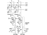
- FIG. 2A is a view for explaining the layout of the unit cell of the present invention shown in FIG. 1, the configuration of the motion detection circuit, and the driving method.
- components having the same function are denoted by the same number.
- the arrangement of the pixels is 2 ⁇ 2 four pixels (pixel 1 (a11), pixel 1 (a′11), pixel 1 (b′11), pixel 1 (b11)).
- the cell is configured.
- Different readout wirings are applied to the readout gates 2, 2 ′ of the pixel 1 (a11) and the pixel 1 (a′11) which are paired in the horizontal direction, respectively, and the remaining horizontal direction Separate read wirings (READ2 ′, READ2) are applied to the gates of the read transistors 2 ′, 2 of the pixel 1 (b′11) and pixel 1 (b11) which are paired with each other. Further, the pixel 1 (a11) and the pixel 1 (b′11) adjacent in the vertical direction are connected to the vertical signal line 6, and the other pixel 1 (a′11) and the pixel 1 (b11) adjacent to each other in the vertical direction are connected. Reading is performed by being connected to another vertical signal line 6 ′.
- LOAD Tr load transistor
- the potential of Tr is connected to the positive side of the capacitor and the differential amplifier circuit 15 via the switch circuit (SW1).
- the potential of LOAD Tr is also connected to the negative side of the differential amplifier circuit 15 through the amplifier 16 via the switch circuit (SW2).
- the output of the differential amplifier 15 is referred to as a differential output 17. If the amplifier 16 is removed from this circuit configuration, it is a CDS (Correlated Double Sampling) circuit configuration generally employed in conventional CMOS sensors.
- CDS Correlated Double Sampling
- the addition output 19 enters the noise removal circuit 20, and the noise removal addition output 21 is connected to the input side of the horizontal readout gate 11 connected to the horizontal signal line 12.
- the noise removal circuit 20 can be replaced by the above-described CDS circuit configuration.
- the noise removal addition output 21 may be connected to the input side of the horizontal readout gate 11 after passing through the ADC circuit 8 in the same manner as the vertical signal lines 6 and 6 ′.
- LOAD The potential of Tr extends to the vertical signal lines 6 and 6 ′ and is connected to the ADC circuit 8 through the switch circuit (SW 3).
- SW 3 switch circuit
- a normal CDS circuit configuration is inserted between the switch circuit (SW 3) and the ADC circuit 8.
- the CDS operation can be performed by ADC digital processing.
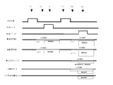
- FIG. 2B shows the photoelectric conversion time change of the output level of the pair of pixel 1 (a11), pixel 1 (a′11), and another pair of pixel 1 (b′11) and pixel 1 (b11).
- FIG. 2B shows the photoelectric conversion time change of the output level of the pair of pixel 1 (a11), pixel 1 (a′11), and another pair of pixel 1 (b′11) and pixel 1 (b11).
- the photoelectric conversion efficiency (referred to as sensitivity in the following description and corresponding to the slope of the graph in the figure) of the pixel is different from that of the pair of pixel 1 (a11) and pixel 1 (a'11).
- the same pixel 4 (b'11) and pixel 1 (b11) have the same four pixels.
- the photoelectric conversion times (referred to as first photoelectric conversion times) of the first pixel 1 (a11) and the pixel 1 (b11) adjacent in the oblique direction are made the same.
- the remaining photoelectric conversion times (referred to as second photoelectric conversion times) of the second pixel (a11 ′) and pixel 1 (b′11) adjacent in the diagonal direction are also set to be the same, and the second photoelectric conversion time is set to the first photoelectric conversion time. It is longer than the time t1 (in the figure, the photoelectric conversion time is doubled).
- READ1 and 2 pulses for discarding the pixel signal are applied to the gate of the read transistor 2 for controlling the photoelectric conversion time of the first pixel 1 (a11) and the pixel 1 (b11), and the potential of the floating junction 3 is applied.
- a reset pulse (indicated by RS in the figure) is applied to the gate of the reset transistor 4.
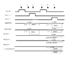
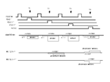
- FIG. 2C is a diagram for explaining the driving method of the present invention, and in particular, a diagram for explaining a sequence of reading out signal output from the pixels at the end of two substantially identical photoelectric conversion times. It is. A timing chart generated in each signal line and pulse line is shown.
- the floating junction 3 is reset (RESET) to a constant voltage via the gate of the reset transistor 4 before the signal charge is transferred (timing T1; hereinafter abbreviated as T1).
- T1 timing T1; hereinafter abbreviated as T1
- the induction of the reset pulse is superimposed on the floating junction 3 as noise, and noise components appear on the vertical signal lines 6 and 6 '(T2).
- the charges that are photoelectrically converted and accumulated in the first pixel 1 (a11) and the pixel 1 (b11) in the first photoelectric conversion time t1 are applied to the readout gate 2 by applying pulses of the readout wirings (READ1, 2). Thus, it flows into the floating junction 3 (T3).
- the signal components of the pixel 1 (a11) and the pixel 1 (b11) are superimposed on the vertical signal lines 6 and 6 'where the noise component is output.
- SW1 is closed (ON), and the output levels of the vertical signal lines 6 and 6 'are held in the capacitors.
- SW1 is opened (OFF)
- the floating junction 3 is reset (T4). In this case as well, the induction of the reset pulse is superimposed as noise, and noise components appear on the vertical signal lines 6 and 6 '(T5).
- the electric charges photoelectrically converted and accumulated in the second pixel (a11 ′) and the pixel 1 (b′11) in the second photoelectric conversion time t2 (2 ⁇ t1) are read out wirings (READ1 ′, 2 ′). Is applied to the read gate 2 ′, and flows into the floating junction 3 (T6).
- the signal components of the pixel 1 (a'11) and the pixel 1 (b'11) are superimposed on the vertical signal lines 6 and 6 'where noise components are output.
- SW2 is closed (ON)
- the output level of the vertical signal lines 6 and 6 ′ is amplified by the amplifier 16, and the differential amplifier circuit 15 is brought to the negative side. input.
- the gain of this amplifier is 1 ⁇ 2, which is the ratio of the first photoelectric conversion time and the second photoelectric conversion time in the above case.
- the signal components of the pixel 1 (a11) and the pixel 1 (b11), which are stored in the capacitors, are input to the plus side of the differential amplifier circuits 15 and 15 ', respectively.
- the signal components of the pixel 1 (a′11) and the pixel 1 (b′11) multiplied by the gain are input to the minus side of the differential amplifier circuits 15 and 15 ′. Therefore, the differential outputs 17 and 17 ′, which are the outputs of the differential amplifiers 15 and 15 ′, are the difference between the pixel 1 (a11) and the pixel 1 (b′11), the pixel 1 (b11), and the pixel, respectively. A difference of 1 (a′11) is output.
- a plurality of pixels are arranged in a matrix to form an imaging screen, and the first and second pixels that are spatially close to each other are taken as one set, and the first pixel 1 photoelectric conversion time t1 is made shorter than the second photoelectric conversion time t2 of the second pixel, the end points of the first and second photoelectric conversion times are substantially matched, and after the first and second photoelectric conversion times, Both the signals of the first and second pixels are read out, the product of the ratio of the first photoelectric conversion time to the second photoelectric conversion time and the signal of the second pixel is obtained, and based on the difference between this product and the signal of the first pixel The movement of the object on the imaging screen can be detected.
- the outputs of the vertical signal lines 6 and 6 ′ are input to the ADC circuit 8 through the CDS circuit (not shown) by closing (ON) the switch circuit (SW3), and converted into, for example, a 10-bit digital signal. Output.
- pixel 1 (a11) and pixel 1 (b11) are combined as the first pixel
- pixel 1 (a′11) is combined as the second pixel. Since the pixels 1 (b′11) are combined, the horizontal scanning lines come out in a zigzag pattern shifted by one line even if they are said sequentially.
- it is output as a composite image of images that are two times different from the output. This is an image output in a mode with an expanded dynamic range. In order to output in the same way as usual, it is necessary to slightly change the circuit as shown below.
- FIG. 2 (d) is related to a method for preventing the output from being output as a composite image of images that differ by twice the output.
- the vertical signal lines 6 and 6 ' are provided with a switch circuit (SW3).
- a switch circuit (SW4) is installed, and an amplifier 22 is installed at the end. Connect the tip to the tip of SW3.
- SW3 When reading the second pixel (for example, pixel 1 (a′11), pixel 1 (b′11)) of the second photoelectric conversion time, SW3 is opened (OFF), SW4 is closed (ON), and SW4 By setting the gain of the previous amplifier to 1 ⁇ 2, in the case of imaging a subject with the same brightness, the output of each pixel can be made the same.
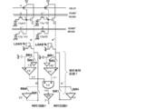
- 3 (a) is similar to FIG. 2 (d), the difference being the LOAD at the end of the vertical signal line 6 ′.
- This is a circuit after Tr, and an amplifier 16 'is inserted between the switch circuit (SW1) and the positive side of the capacitor and the differential amplifier circuit 15, and is connected to the negative side of the differential amplifier 15', and is connected to the switch circuit SW2 side. Is connected to the positive side of the differential amplifier 15 'without being inserted.
- FIG. 3B shows the photoelectric conversion time change of the output level of the pair of pixel 1 (a11) and pixel 1 (a′11) and another pair of pixel 1 (b′11) and pixel 1 (b11). It is a figure and is the same as FIG.2 (b).
- READ1 and 1 ' are read at the same timing, and the pixels 1 (a11) and 1 (a'11) adjacent in the horizontal direction are simultaneously transferred to the vertical signal lines 6 and 6'.
- SW2 is opened (OFF), SW1 is closed (ON), and the capacitor holds the potential of the vertical signal line.
- READ2 and 2 ' are read out at the same timing at the next timing, and pixel 1 (b'11) and pixel 1 (b11) adjacent in the horizontal direction are simultaneously transferred to the vertical signal lines 6 and 6'.
- SW1 is opened (OFF), SW2 is closed (ON), and the differential amplifiers 15 and 15 'take the difference.
- the signal component of the pixel 1 (a11) stored in the capacitor is on the plus side of the differential amplifier circuit 15, and the pixel 1 (a′11) stored in the capacitor is on the minus side of the differential amplifier circuit 15 ′. ) Is multiplied by the gain of the amplifier 16 '. On the negative side of the differential amplifier circuit 15, the signal component of the pixel 1 (b'11) multiplied by the gain is provided. On the positive side of the differential amplifier circuit 15 ', the signal component of the pixel 1 (b11) is provided. Have been entered.
- the differential outputs 17 and 17 ′ which are the outputs of the differential amplifiers 15 and 15 ′, are the difference between the pixel 1 (a11) and the pixel 1 (b′11), the pixel 1 (b11), and the pixel, respectively.
- a difference of 1 (a′11) is output.
- the difference from 1 ⁇ 2 of the pixel 1 (b′11) is the summed output 19 of the summing circuit 18.
- An output obtained by processing this with the noise removal circuit 20 having the CDS circuit configuration is output as a noise removal addition output 21. This is the same as the description of FIG.
- the second pixel for example, pixel 1 (a′11), pixel 1 (b′11) in the second photoelectric conversion time. Is gained by the amplifier 22, and is input to the ADC circuit with the same output as the first pixel (for example, the pixel 1 (a11) and the pixel 1 (b11)) in the first photoelectric conversion time. Reading from the pair of pixels 1 (a11) and 1 (a'11) on the same horizontal scanning line simultaneously with READ1 and 1 'is performed in the ADC circuit, which is the same as the line sequential reading in a normal CMOS sensor. You can do it.
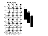
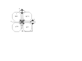
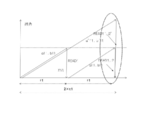
- FIG. 4A is a diagram showing the repetitive arrangement of unit cells in the motion detection imaging apparatus according to the present invention shown in FIGS. 2A and 3A.
- FIG. 4A shows coordinate positions of A, B, C, and D in the horizontal direction and 1, 2, 3, 4, 5, 6, 7, and 8 in the vertical direction as pixel coordinates.
- a diagram in which the positions of the object end portion of the subject and the pixel arrangement are changed is also attached.
- the object end of the black pattern subject extends in the horizontal direction, and the end position in the vertical direction is at the boundary between coordinates 2 and 3 on the upper side and coordinates 5 and coordinates on the lower side.
- the state at the boundary of 6 is defined as an initial state.
- Timing 1 is a timing immediately after resetting of pixels (for example, a11, a12, b11, and b12) to which movement for one pixel is completed and no '(dash) is added.
- Timing2 A case in which the object of the subject moves further downward by one pixel during the next first photoelectric conversion time t1 is indicated by Timing2.
- the movement for two pixels is completed in the movement period of 2 ⁇ t1, and the timing immediately before the reading from the pixel is Timing2. It is assumed that the movement of the subject is performed at a constant speed.
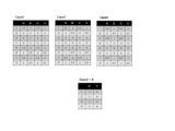
- FIG. 4 (b) shows what kind of output is obtained at each pixel at each coordinate at the three timings (Initial, Timing1, Timing2) shown in FIG. 4 (a), and motion detection is performed by calculating them.
- the table shows how the signal looks.
- the second photoelectric conversion time t2 is twice as long as the first photoelectric conversion time t1
- the pixel output is zero in the black pattern portion
- the second photoelectric conversion time corresponds to the second photoelectric conversion time in the portion other than the black pattern.
- the output of all the pixels (pixels marked with ') is 1, and the output of the pixels corresponding to the first photoelectric conversion time (pixels not marked with') is 0.5.
- the black pattern end moves from the upper end to the lower end of the pixel (coordinates) during the first photoelectric conversion time, or when the entire surface is exposed during the first photoelectric conversion time
- the corresponding pixel output is set to half of 0.5.
- the incident intensity to the pixel when the end of the black pattern comes to the center of the pixel (coordinates) is half that when the entire surface is exposed.
- the initial timing is immediately after the start of photoelectric conversion, so the output of all the pixels is zero.
- the pixel corresponding to the first photoelectric conversion time is 0.5 for a pixel that is exposed on the entire surface, and is 0 for a pixel that corresponds to a black pattern and is not exposed.
- the output is 0.25.
- the pixel corresponding to the second photoelectric conversion time it is 1 for the pixel that is exposed to the whole surface during the second photoelectric conversion time, and 0 for the pixel that corresponds to the black pattern and is not exposed.
- the output is 0.75.
- the edge of the black pattern is moved at Timing 1 and the output becomes 0.25 in the darkened pixels (b′31 and b′32).
- the edge of the black pattern is moved and brightened at Timing 2.
- the pixel (b′21, b′22) is 0.25, and the darkened pixel (a′41, a′42) is 0.75.
- the calculation method is a method of calculating a difference after converting the sum of the multiplying pixels and the sum of the remaining multiplying pixels into a photoelectric conversion time.
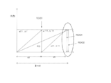
- FIG. 5A is a diagram showing the repetitive arrangement of unit cells in the same motion detection imaging apparatus according to the present invention as in FIG. FIG. 5A also shows the coordinate positions of A, B, C, and D in the horizontal direction and 1, 2, 3, 4, 5, 6, 7, and 8 in the vertical direction as pixel coordinates.
- the output position of the motion detection signal when the object of the subject does not move is determined, and the object position of the subject is set one pixel up and down around the initial position in FIG. Estimate the 3 cases that have moved.
- FIG. 5A also includes a diagram in which the relative position between the object end of the subject and the pixel arrangement is changed.
- Case 1 the end of the black pattern extends in the horizontal direction, and the position of the end of the vertical direction is the boundary between the coordinates 1 and 2 on the upper side and the boundary between the coordinates 4 and 5 on the lower side. If you come to. Cases 2 and 3 were obtained when the black pattern was sequentially shifted downward by one pixel from Case 1. In Cases 1, 2 and 3, the black object remains stationary.
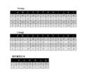
- FIG. 5 (b) is a table showing the output of each pixel at each coordinate in the case of Cases 1, 2, and 3, and the motion detection signal obtained by calculating them. Yes.
- the preconditions for calculating this output are the same as those in FIG.
- FIG. 5B shows a table showing output values generated in pixels of each coordinate for each case (Case1, Case2, Case3) of the black pattern position of the subject.
- a motion detection signal is calculated from Cases 1, 2, and 3.
- this calculation is applied to all the pixel blocks, all are 0.
- other Cases are 0, and these results are shown in Cases 1, 2, and 3 at the bottom of FIG. Since only one motion signal is output to each pixel block (2 ⁇ 2 pixels), the table of motion signal output is halved both in the horizontal direction and in the vertical direction. It becomes a table
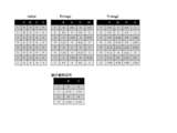
- a Bayer arrangement method that is usually used is a basic arrangement of 2 (horizontal) ⁇ 2 (vertical) pixels, and the color filter has two adjacent green (G) pixels in the diagonal direction and the remaining red (R ) And blue (B) pixels.
- the two G are distinguished by changing the horizontal line of R with Gr and the horizontal line of B with Gb.
- FIG. 6 is a diagram showing the overall configuration of a motion detection color imaging apparatus according to the present invention.
- the feature of the arrangement of the solid-state imaging device pixels for motion detection according to the present invention in which 2 ⁇ 2 4 pixels form one cell is also advantageous in color imaging.
- color filters of the same color are arranged.
- Green hereinafter abbreviated as G, g, Red line on Gr, gr, and Blue line on Gb, gb
- G Green
- G Green
- G′11 Green
- pixel 1 (gr′11) Green
- gr′11 Green
- pixel 1 (gr′11) Green
- gr′11 Green
- gr′11 Green
- gr11 Green
- Blue corresponds to each of the pixel cells, and is indicated by pixel 1 (B11), pixel 1 (B′11), pixel 1 (b′11), and pixel 1 (b11).
- Green on the remaining Blue line is also indicated as pixel 1 (Gb11), pixel 1 (Gb′11), pixel 1 (gb′11), and pixel 1 (gb11).
- the pixel arrangement in FIG. 6 is arranged in the vertical and horizontal directions in units of 16 pixels in which 2 ⁇ 2 pixels and one color block are Bayer arranged in 2 ⁇ 2. This color filter is called Quad Bayer.
- FIGS. 1 to 5 the motion detection method has been described by not considering the color filter arrangement. However, in the color filter arrangement of FIG. 6, the processing is performed in the pixel block of the same color. The results of motion detection 1 to 5 can be similarly applied to FIG.
- the pixel 1 (Gr11), the pixel 1 (Gr′11), the pixel 1 (R11), and the pixel 1 (R′11) that are paired in the horizontal direction have different readouts for the readout gates 2 and 2 ′.
- Wirings (READ1, READ1 ′) are applied to change the photoelectric conversion time within the same color pixel (for example, Gr11, Gr′11).
- the pixel 1 (gr′11), the pixel 1 (gr11), the pixel 1 (r′11), and the pixel 1 (r11), which are paired in the horizontal direction of the next line have different readout wirings.
- the photoelectric conversion time is changed within the same color pixel (for example, gr′11, gr11).
- the first photoelectric conversion times of the first pixel 1 (Gr11) and the pixel 1 (gr11) adjacent in the oblique direction are made the same.
- the second photoelectric conversion time of the second pixel 1 (gr′11) and the pixel 1 (Gr′11) adjacent in the remaining diagonal direction is also made the same, and the second photoelectric conversion time is made longer than the first photoelectric conversion time. (For example, the photoelectric conversion time is doubled). This situation is the same as in FIG. Similarly, the photoelectric conversion time of 2 ⁇ 2 pixels in the other color blocks is also changed.
- the circuit configuration at the lower ends of the vertical signal lines 6 and 6 ' is the same as that shown in FIG.
- the driving method of the motion detection color imaging apparatus according to the present invention shown in FIG. 4 is the same as that shown in FIG. 1, and a color digital signal is output from the ADC circuit 8 and a motion detection signal is output from the horizontal signal line 12.
- FIGS. 7A and 7B are diagrams illustrating how the motion detection signal changes when the object position of the subject changes in the motion detection color imaging apparatus according to the present invention.
- FIG. 7A is a diagram showing a repetitive arrangement of color blocks based on a specific component drawing of the motion detection color imaging apparatus according to the present invention shown in FIG.
- the pixel 1, the gate of the readout transistor 2, the floating junction 3, the gate of the reset transistor 4, the gate of the amplification transistor 5, and the vertical signal lines 6 and 6 ', which are the basic configuration of FIG. 6, are shown with reference to an actual layout diagram. .
- One pixel cell in FIG. 1 corresponds to a color block.
- Corresponding color blocks (Gr11, Gr′11, gr′11, gr11).
- FIG. 6A shows coordinate positions of A, B, C, and D in the horizontal direction and 1, 2, 3, 4, 5, 6, 7, and 8 in the vertical direction as pixel coordinates.
- FIG. 7A also includes a diagram in which the relative position between the object end of the subject and the pixel arrangement is changed.
- Case 1 the black object end portion extends in the horizontal direction, and the vertical end portion position is at the center of coordinate 3 on the upper side and at the center of coordinate 6 on the lower side. Is in the initial state.
- Timing1 is the timing immediately after the movement for one pixel is completed and reset.
- Timing2 is the timing immediately after the movement for one pixel is completed and reset.
- Timing2 A case in which the object moves further downward by one pixel during the next first photoelectric conversion time t1 is indicated by Timing2.
- FIG. 4A the movement for two pixels is completed in the movement period of 2 ⁇ t1, and the timing immediately before the reading from the pixel is Timing2. It is assumed that the object movement of the subject is performed at a constant speed.
- FIG. 7 (b) shows the output of each pixel at each coordinate at the three timings (Initial, Timing1, and Timing2) shown in FIG.
- the table shows how the signal looks. In calculating this output, the same preconditions as in FIG. Details are obtained by the same calculation method as in FIG. 4B, and only the result is described as a table corresponding to three timings (Initial, Timing1, and Timing2).
- a motion detection signal is generated at the contour portion of the moving object.
- the motion detection signal output pattern table is halved in both the horizontal and vertical directions, and is a 2 ⁇ 4 table in FIG. 7B.
- FIG. 8A is a diagram showing the repetitive arrangement of unit cells in the same motion detection imaging apparatus according to the present invention as in FIG. 7A.
- FIG. 8A also shows the coordinate positions of A, B, C, and D in the horizontal direction and 1, 2, 3, 4, 5, 6, 7, and 8 in the vertical direction as pixel coordinates.
- the output pattern of the motion detection signal when the object of the subject does not move is determined, and the object position of the subject is set one pixel up and down around the initial position in FIG. 7A. Estimated for 3 cases moved.
- FIG. 8A also includes a diagram in which the relative position between the object end of the subject and the pixel arrangement is changed.
- Case 4 the end of the black object extends in the horizontal direction, and the end position in the vertical direction comes to the center of coordinate 2 on the upper side and to the center of coordinate 5 on the lower side. If you are. Cases 5 and 6 were obtained when the black object was sequentially shifted downward by one pixel from Case 4. The black objects in both Cases 4, 5, and 6 remain stationary.
- FIG. 8B is a table showing what kind of output is obtained in each pixel at each coordinate in the case 4, 5, 6, and what the motion detection signal obtained by calculating them is. Yes.
- the preconditions for calculating this output are the same as those in FIG. Details are obtained by the same calculation method as in FIG. 5B, and only the result is described.
- the output pattern table of the motion detection signal is half in both the horizontal and vertical directions.
- FIG. 8B shows a 2 ⁇ 4 table. The calculation results are all 0 for every color block.
- the object of the subject is a black object whose end extends in the left-right direction, and when the black object is moved in the up-down direction and the relative position in the up-down direction with respect to the pixel is changed.
- the calculation result was as follows. The same calculation is possible even when the object end of the subject extends in the vertical direction and moves in the horizontal direction with respect to the pixel array.
- the multiplication operation is performed with 2 ⁇ 2 pixel cells in the pixel block, and the result is equivalent.
- FIG. 9 is a diagram showing an overall configuration of a motion detection color imaging apparatus according to another embodiment of the present invention.
- the arrangement of the solid-state imaging device pixels for motion detection of the present invention is a configuration in which the floating junction 3, the amplifying transistor 5, and the reset transistor 4 are shared by the four pixels while maintaining the characteristic that one cell is formed by 2 ⁇ 2 pixels. It is.
- the color filter arrangement for each color block is the same as in FIG.
- the upper left block includes pixel 1 (Gr11), pixel 1 (Gr′11), pixel 1 (gr′11), and pixel 1 (gr11) corresponding to each pixel cell.
- the pixel 1 (Gr11), the pixel 1 (Gr′11), the pixel 1 (R11), and the pixel 1 (R′11) that are paired in the horizontal direction have different readouts for the readout gates 2 and 2 ′.
- Wirings (READ1, READ1 ′) are applied, and the photoelectric conversion time is changed within the same color pixel (for example, Gr11, Gr′11) as in FIG.
- the pixel 1 (gr′11), the pixel 1 (gr11), the pixel 1 (r′11), and the pixel 1 (r11), which are paired in the horizontal direction of the next line have different readout wirings.
- the 2 ⁇ 2 pixel photoelectric conversion time in other color blocks is similarly changed.
- the circuit configuration at the lower end of FIG. 9 is slightly different from that of FIG. However, this is a difference in configuration in the motion detection circuit 7 and the ADC circuit 8, and the horizontal scanning circuit 13, the vertical scanning circuit 14, the horizontal readout gate 11, and the horizontal readout line 12 are the same as those in FIG.
- a color digital signal is output from the ADC circuit 8 and a motion detection signal is output from the horizontal signal line 12.
- FIG. 10 is a diagram showing the basic unit configuration of the color block based on the specific component drawing of the motion detection color imaging apparatus of the present invention of FIG.
- the pixel 1 of the Green color block shown as an example is composed of four pixels Gr11, Gr′11, gr′11, and gr11.
- the read gates 2 and 2 ', the floating junction 3, the gate of the reset transistor 4 and the gate of the amplification transistor 5 are arranged as shown in FIG.
- the output circuit portion can be shared by four pixels, and the degree of integration can be improved.
- FIGS. 11A, 11B, and 11C are diagrams for explaining the 2 ⁇ 2 basic pixel block and the circuit ahead of the vertical signal line in FIG. 9 and driving. As a general form, the figure is described with a configuration without a color filter in contrast to FIG.
- FIG. 11A is a diagram for explaining the unit cell layout, motion detection circuit configuration, and driving method according to another embodiment of the present invention shown in FIG.
- the arrangement of the pixels is 2 ⁇ 2 four pixels (pixel 1 (a11), pixel 1 (a′11), pixel 1 (b′11), pixel 1 (b11)) to form one cell.
- Different readout wirings are applied to the readout gates 2, 2 ′ of the pixel 1 (a11) and the pixel 1 (a′11) which are paired in the horizontal direction, respectively, and the remaining horizontal direction
- Different readout wirings (READ2 ′, READ2) are applied to the readout gates 2 ′, 2 of the pixel 1 (b′11) and the pixel 1 (b11) which are paired with each other.
- the charges of the four pixels flow into one floating junction 3 and are read out by the vertical signal line 6.
- a branch is made to several circuits from the junction of the end of the vertical signal line 6 to the LOAD Tr (load transistor).
- LOAD The potential of Tr is connected to the positive side of the capacitor and the differential amplifier circuit 15 through the switch circuit (SW1).
- the potential of LOAD Tr is also connected to the negative side of the differential amplifier circuit 15 through the amplifier 16 via the switch circuit (SW2).
- the output of the differential amplifier 15 is referred to as a differential output 17. This differential output constitutes a motion detection signal.
- the amplifier 22 performs a function of aligning pixel outputs having different photoelectric conversion times. Specifically, since pixel outputs having different photoelectric conversion times alternately appear, in synchronization with this, SW3 and SW4 are changed, and pixels having a long photoelectric conversion time (a′11 and b′11 in the figure). Is half the output through amplifier 22.
- FIG. 11B shows the photoelectric conversion time change of the output level of the pair of pixel 1 (a11) and pixel 1 (a′11) and another pair of pixel 1 (b′11) and pixel 1 (b11).
- FIG. 11C is a diagram for explaining the timing of RESET, READ1, 1 ′, READ2, 2 ′, output change appearing on the vertical signal line, and differential output.
- the pixel 1 (a11) and the pixel 1 (a′11) adjacent in the horizontal direction are sequentially applied to READ1, 1 ′, and a read pulse is applied (timing T1, T2), and transferred to the vertical signal line 6.
- the output of the vertical signal line 6 and the output of the vertical signal line 6 ′ at the point of joining after passing through the amplifier 22 are shown in the figure. Since the difference in photoelectric conversion time is corrected, normal imaging output is obtained, and serial input to the ADC circuit.
- the ADC circuit sequentially outputs a11 and a′11.
- the waveform of the differential output 17 in FIG. 11A is as shown in FIG. 11C, but by taking the difference between the two (a circuit is not shown), a motion signal is output.
- the noise component is added to the differential output 17 ', the noise component can be easily removed through a normal CDS circuit (not shown).
- the present invention is effective even in the 4-pixel 1-cell configuration in which the output circuits shown in FIGS. 9 and 10 are shared, and both the normal image signal and the motion detection signal can be output.
- the pixel sizes described above are all the same, and the sensitivity is assumed to be the same for the same color.
- the output difference changes twice. For this reason, the signal is reduced to 1 ⁇ 2 with an amplifier, and the output is made uniform to obtain a difference signal to obtain a motion detection signal.
- Providing an amplifier for each column not only complicates the configuration of the motion detection circuit, but also increases power consumption.
- FIGS. 12A, 12B, and 12C are diagrams illustrating the layout of a unit cell, the configuration of a motion detection circuit, and a driving method according to another embodiment of the present invention.
- the arrangement of the pixels is 2 ⁇ 2 four pixels (pixel 1 (a11), pixel 1 (a′11), pixel 1 (b′11), pixel 1 (b11)) to form one cell.
- Different readout wirings (READ1, READ1 ′) are applied to the gates of the readout transistors 2 and 2 ′ of the pixel 1 (a11) and the pixel 1 (a′11) which are paired in the horizontal direction, respectively.
- the first pixel set (pixel 1 (a11), pixel 1 (b11)) of the first photoelectric conversion time and the second pixel set (pixel 1 (b) of the second photoelectric conversion time. '11), the pixel size of the pixel 1 (a'11)) is changed, and the sensitivity is changed.
- the sensitivity of the second pixel group is set to 1 ⁇ 2 times the sensitivity of the first pixel group while the second photoelectric conversion time is set to twice the first photoelectric conversion time will be described. .
- FIG. 12B is a diagram illustrating the photoelectric conversion time change of the output level of the pixel 1 (a11), the pixel 1 (a′11), the pixel 1 (b′11), and the pixel 1 (b11).
- the sensitivity of the first pixel group (pixel 1 (a11), pixel 1 (b11)) is high, and reset (RS) is performed halfway.
- the first pixel group has a double sensitivity, but has a feature that the photoelectric conversion time is halved. For this reason, the output of the first pixel group and the second pixel group is the same at the readout timing.
- FIG. 12C shows the driving method of the embodiment shown in FIGS. 12A and 12B, and is a diagram for explaining the timing of RESET, READ1, 1 ′, the change in output appearing on the vertical signal line, and the differential output. It is.
- the pixel 1 (a11) and the pixel 1 (a'11) adjacent in the horizontal direction are sequentially applied to READ1, 1 ', and a read pulse is applied (timing T6, T8), and transferred to the vertical signal line 6. Since the difference between the output of the vertical signal line 6 and the photoelectric conversion time is originally corrected by the sensitivity of the pixel, it becomes a normal imaging output and enters the ADC circuit serially.
- the ADC circuit sequentially outputs a11 and a′11.
- the motion detection signal processing circuit at the end of the vertical signal line 6 is composed of a circuit similar to the CDS circuit. This is because the difference in photoelectric conversion time is not the difference in output, so that an amplifier is unnecessary and the circuit is simplified.
- the waveform of the differential output 17 is as shown in FIG. This is because the amplifier is no longer necessary, and the reset noise components are the same and can be eliminated by the difference.
- the same processing is performed at b′11 and b11, and the motion detection circuit signal of the present invention can be obtained by combining with the calculation results of a11 and a′11. As described above, even in the 4-pixel 1-cell configuration in which the output circuit shown in FIG. 12 is shared, the present invention is effective and can output both a normal image signal and a motion detection signal.
- FIG. 13 is a diagram showing a repetitive arrangement of color blocks based on a specific component drawing of the motion detection color imaging apparatus having a 4-pixel 1-cell configuration sharing the output circuit shown in FIG.
- the 4-pixel 1-cell configuration sharing the output circuit is based on FIG. 10, and the sensitivity difference between the pixels of FIG. 13 is expressed by changing the pixel size.
- the size of the normal pixel size is controlled by the size of the microlens on the top surface of the pixel.
- the arrangement of the color filters is the same as in FIG.
- FIG. 14 is a repetitive configuration in which an output circuit is efficiently arranged based on a specific component drawing of the motion detection color imaging device having a 4-pixel 1-cell configuration in which the output circuit shown in FIG. 13 is shared.
- FIG. The driving method and the like are the same as in FIG.
- FIG. 15A is a diagram showing the repetitive arrangement of unit cells in the detection imaging apparatus according to the present invention shown in FIG. The fact that the direction of movement can be easily determined according to the present invention will be described below.
- the coordinates of the pixel are A, B, C, D, E, F, G, H, I, J, K, L in the horizontal direction, 1, 2, 3, 4 in the vertical direction. The coordinate position is shown.
- FIG. 15A also includes a diagram in which the positions of the black object end of the subject and the pixel arrangement are changed.
- the end of the black object extends in the vertical direction
- the horizontal end position is at the boundary between the B coordinate and the C coordinate on the left side
- the boundary between the H coordinate and the I coordinate on the right side is indicated by Timing1.
- Timing 1 is the timing when the movement for two pixels is completed.
- Timing2 a case where the object further moves to the right side by two pixels.
- the timing when the movement of 4 pixels is completed in the 2 ⁇ t1 movement period is Timing2. It is assumed that the movement of the object is performed at a constant speed.
- FIG. 15 (c) shows the output of each pixel at each coordinate at the three timings (Initial, Timing1, Timing2) shown in FIG.
- the table shows how the signal looks.
- the second photoelectric conversion time is set to be twice as long as the first photoelectric conversion time
- the pixel output of the black object is zero
- the pixel corresponding to the second photoelectric conversion time (other than the black object)
- the output of the pixel marked with ' is set to 1.
- Other preconditions are the same as those in FIG.
- the pixels corresponding to the first photoelectric conversion time (a11, a12, a13,..., B11, b12, b13%) are immediately read out and reset in Timing1. 0.
- the pixels corresponding to the second photoelectric conversion time (a′11, a′12, a′13, b′11, b′12, b′13.
- Timing 1 and Timing 2 are as shown in the table of FIG.
- the motion detection signal is calculated from this Timing 2, the detailed description is omitted, but the table of the motion detection signal is obtained.
- the direction of movement is expressed by a sign of ⁇ .
- the sign of the head part of the movement is minus, and the sign of the tail part of the movement is plus.
- the sign plus and minus are reversed. That is, in the present application, at the same time as the motion detection information appears in the peripheral portion of the moving object, the direction of motion can be detected by the code.
- the code for the direction of movement of the subject was confirmed in the actual imaging state, and as expected, the difference in the calculated code was confirmed at the edge of the moving subject.
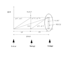
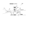
- FIG. 16 is a diagram showing the overall configuration of a motion detection system to which the present invention is applied.
- the motion detection system 30a of the present invention includes an imaging device 32a including an imaging lens 31, a motion determination circuit 33a, a motion determination threshold setting circuit 34 for setting a determination level for determining motion, and an imaging signal of the imaging device 32a.
- a color signal processing circuit 35 for processing the video signal to be reproduced on the monitor, a video signal output circuit 37 for outputting the video signal 1, and a motion determination signal output circuit for outputting the determination result of the motion determination 36 or the like.
- the motion determination threshold value setting circuit 34 sets the level threshold value 1 for counting so as not to count the difference signal of the noise level, and sets the count number to be the threshold value 2. When the count number exceeds this threshold value 2, it is determined that there is a moving object.
- the motion determination circuit 33a counts the number of times that the level of the motion detection signal output from the imaging device 32a is greater than the threshold value 1. If the count number exceeds the threshold 2, it is determined that there is a moving object, and the determination signal ON / OFF is set to the HI level. When there is no movement, the LO level is set.
- the circuit operation and signal processing operation of the color signal processing circuit 35 and the video signal output circuit 37 are stopped. By doing so, the power consumption of the motion detection system 30a can be reduced. Similarly, the power consumption of the imaging device 32a can be reduced by controlling the timing circuit of the imaging device 32a.
- an input signal for color signal processing is cut off. For example, the 10-bit digital value of the input signal is switched to all zeros. Since the signal after the color signal processing circuit becomes zero and the switching operation (0 ⁇ 1 switching) of the digital circuit stops, the power consumption of the circuit operation can be reduced.
- each circuit or device is provided with a reset switch for returning to the original state when a malfunction occurs. By keeping the reset switch in the ON state, the circuit processing of each circuit or device is kept stopped, so that power consumption can be reduced.
- FIG. 17 is an overall configuration diagram showing a modified example of the motion detection system to which the present invention is applied.
- the motion detection system 30b has an advantage that a conventional transmission cable can be used by reducing the motion determination signal output circuit 36 of FIG.
- the motion determination circuit 33b outputs a motion determination signal (ON / OFF) and also outputs a determination code.
- the motion determination signal (ON / OFF) stops the circuit operation and signal processing operation of the color signal processing circuit 35 and the video signal output circuit 37 as in FIG.
- the determination code obtained by coding the ON / OFF signal of the determination signal is embedded in the video signal using the motion determination signal addition circuit 38.
- shooting information different from a video signal is embedded in a blanking period in which a valid video signal is not included.
- the motion determination signal is encoded and embedded in the blanking period to output the video signal 2.
- FIG. 18 is a configuration diagram in which a determination circuit 33a is provided on the horizontal signal line 12 from which a motion detection signal is output in the overall configuration diagram of the motion detection imaging apparatus according to the present invention shown in FIG.
- the determination output signal ON / OFF of the determination circuit 33a is input to the timing generation circuit 24.
- the timing generation circuit 24 By controlling the timing generation circuit 24, it is possible to add a function for changing the driving method of the vertical scanning circuit 14, the horizontal scanning circuit 13, the motion detection circuit 7, the ADC circuit 8, and the like.
- the determination output signal ON / OFF can also be output to the outside. Specific driving methods that can be performed by adding the determination circuit 33a shown in FIG. 18 will be sequentially described below.
- the vertical scanning circuit 14 and the horizontal scanning circuit 13 are controlled by controlling the timing generation circuit based on information from the determination circuit 33a.
- the entire screen is imaged to detect the presence or absence of a moving object.
- the number of scanning lines is thinned out, and the thinned state is maintained until the moving object appears. Since the thinning interval changes depending on the situation, several thinning patterns may be prepared and which one to select may be changed depending on the pattern of the motion detection signal. When a moving object appears, it is sufficient to return to the all-pixel imaging mode again. If the area where the moving object is present is biased, the entire image is divided into blocks, the number of scanning lines is increased only in the area where the moving object exists, and a drive mode is prepared in which the other areas are reduced. It is also possible to select a pattern in the existing area.
- the power source of the signal processing system in the subsequent stage is set to the standby state, and the motion detection signal appears significantly.
- it may be used as an ON / OFF signal for a subsequent power supply that is turned on again. In this way, when there is no movement, a significant energy saving can be achieved by turning off the power of the signal processing circuit in the subsequent stage, in addition to setting the energy saving mode by thinning-out operation of the imaging device.
- the latter stage power is turned on only when there is movement compared to the conventional system that always requires the latter stage processing, and usually only the thinning drive of the imaging apparatus of the present invention is required.
- a large (for example, 1/1000 to 1/100000) energy saving can be realized. This feature is a great advantage when the present invention is applied to a monitoring system in a place where the power supply of the mountainous area does not reach, and reaches a level that can be sufficiently driven by a power supply of a compact solar battery and capacitor set.
- the dynamic range may be expanded by changing the conversion level of the ADC based on the information of the motion detection signal.
- the method of increasing the motion detection signal by changing the photoelectric conversion accumulation period and changing the gain of the amplifier accordingly is described.
- the dynamic range of the normal image can be expanded in the region where the motion detection signal is output. Specifically, by adding two pixels having different photoelectric conversion accumulation times, the dynamic range can be expanded, and the ADC can be set appropriately. The same applies to the method of achieving a high dynamic range by adding pixels having different pixel sizes shown in FIG.
- the motion detection imaging apparatus As described above, it is possible to obtain normal pixel imaging information simultaneously with the motion detection signal, and to determine that normal pixel imaging information is not output to the outside based on the motion information.
- Functions can be provided.
- the function of outputting only the imaging information of the portion with the movement to the outside and not outputting the image information without the movement to the outside is very useful for the surveillance camera application.
- monitoring by a conventional surveillance camera has been a heavy load on the surveillance staff. However, only a camera with motion or only a portion with motion is displayed. This greatly reduces the burden on the observer.
- the ratio of the photoelectric conversion time is not limited to 1: 2, and the ratio can be changed according to the movement of the subject.
- the gain of the amplifier may be changed (amplified or reduced) correspondingly.
- the layouts of the pixel cells in FIGS. 13 and 14 may be arranged rotated by 90 degrees or 45 degrees.
- 2 ⁇ 2 pixels adjacent to each other as a pixel block are set as a cell unit.
- the same calculation process is performed on a 2 ⁇ 2 pixel block of the same color every other pixel. Also good.
- background noise without movement increases, but a conventional Bayer color filter can be used as it is.
- the background noise can be reduced as compared with the conventional calculation only in the horizontal direction.
Landscapes
- Engineering & Computer Science (AREA)
- Multimedia (AREA)
- Signal Processing (AREA)
- Physics & Mathematics (AREA)
- Spectroscopy & Molecular Physics (AREA)
- Solid State Image Pick-Up Elements (AREA)
- Transforming Light Signals Into Electric Signals (AREA)
Applications Claiming Priority (2)
| Application Number | Priority Date | Filing Date | Title |
|---|---|---|---|
| JP2012268874A JP5747238B2 (ja) | 2012-12-07 | 2012-12-07 | 動き検出用固体撮像装置及び動き検出システム |
| JP2012-268874 | 2012-12-07 |
Publications (1)
| Publication Number | Publication Date |
|---|---|
| WO2014087840A1 true WO2014087840A1 (ja) | 2014-06-12 |
Family
ID=50883265
Family Applications (1)
| Application Number | Title | Priority Date | Filing Date |
|---|---|---|---|
| PCT/JP2013/081220 Ceased WO2014087840A1 (ja) | 2012-12-07 | 2013-11-20 | 動き検出用固体撮像装置及び動き検出システム |
Country Status (2)
| Country | Link |
|---|---|
| JP (1) | JP5747238B2 (enExample) |
| WO (1) | WO2014087840A1 (enExample) |
Cited By (3)
| Publication number | Priority date | Publication date | Assignee | Title |
|---|---|---|---|---|
| US10536657B2 (en) | 2016-03-18 | 2020-01-14 | Semiconductor Energy Laboratory Co., Ltd. | Imaging device and electronic device |
| WO2023276564A1 (ja) * | 2021-06-28 | 2023-01-05 | 株式会社SEtech | 動き情報撮像装置 |
| WO2023065197A1 (zh) * | 2021-10-21 | 2023-04-27 | 华为技术有限公司 | 运动目标检测方法、装置以及检测设备 |
Families Citing this family (4)
| Publication number | Priority date | Publication date | Assignee | Title |
|---|---|---|---|---|
| JP6555956B2 (ja) * | 2014-07-31 | 2019-08-07 | 株式会社半導体エネルギー研究所 | 撮像装置、監視装置、及び電子機器 |
| US10348991B2 (en) | 2015-03-17 | 2019-07-09 | Sony Corporation | Solid-state image pickup device with load transistors, method for controlling the same, and electronic apparatus |
| KR102553553B1 (ko) * | 2015-06-12 | 2023-07-10 | 가부시키가이샤 한도오따이 에네루기 켄큐쇼 | 촬상 장치, 및 그 동작 방법 및 전자 기기 |
| US11405535B2 (en) | 2019-02-28 | 2022-08-02 | Qualcomm Incorporated | Quad color filter array camera sensor configurations |
Citations (3)
| Publication number | Priority date | Publication date | Assignee | Title |
|---|---|---|---|---|
| WO2012008143A1 (ja) * | 2010-07-12 | 2012-01-19 | パナソニック株式会社 | 画像生成装置 |
| JP2012094984A (ja) * | 2010-10-25 | 2012-05-17 | Nikon Corp | 撮像装置 |
| JP2012175621A (ja) * | 2011-02-24 | 2012-09-10 | Sony Corp | 画像処理装置、および画像処理方法、並びにプログラム |
Family Cites Families (3)
| Publication number | Priority date | Publication date | Assignee | Title |
|---|---|---|---|---|
| US7583305B2 (en) * | 2004-07-07 | 2009-09-01 | Eastman Kodak Company | Extended dynamic range imaging system |
| JP4246244B2 (ja) * | 2007-09-14 | 2009-04-02 | オリンパス株式会社 | 撮像装置 |
| JP4582198B2 (ja) * | 2008-05-30 | 2010-11-17 | ソニー株式会社 | 固体撮像装置、撮像装置、固体撮像装置の駆動方法 |
-
2012
- 2012-12-07 JP JP2012268874A patent/JP5747238B2/ja not_active Expired - Fee Related
-
2013
- 2013-11-20 WO PCT/JP2013/081220 patent/WO2014087840A1/ja not_active Ceased
Patent Citations (3)
| Publication number | Priority date | Publication date | Assignee | Title |
|---|---|---|---|---|
| WO2012008143A1 (ja) * | 2010-07-12 | 2012-01-19 | パナソニック株式会社 | 画像生成装置 |
| JP2012094984A (ja) * | 2010-10-25 | 2012-05-17 | Nikon Corp | 撮像装置 |
| JP2012175621A (ja) * | 2011-02-24 | 2012-09-10 | Sony Corp | 画像処理装置、および画像処理方法、並びにプログラム |
Cited By (4)
| Publication number | Priority date | Publication date | Assignee | Title |
|---|---|---|---|---|
| US10536657B2 (en) | 2016-03-18 | 2020-01-14 | Semiconductor Energy Laboratory Co., Ltd. | Imaging device and electronic device |
| US11330213B2 (en) | 2016-03-18 | 2022-05-10 | Semiconductor Energy Laboratory Co., Ltd. | Imaging device and electronic device |
| WO2023276564A1 (ja) * | 2021-06-28 | 2023-01-05 | 株式会社SEtech | 動き情報撮像装置 |
| WO2023065197A1 (zh) * | 2021-10-21 | 2023-04-27 | 华为技术有限公司 | 运动目标检测方法、装置以及检测设备 |
Also Published As
| Publication number | Publication date |
|---|---|
| JP2014116762A (ja) | 2014-06-26 |
| JP5747238B2 (ja) | 2015-07-08 |
Similar Documents
| Publication | Publication Date | Title |
|---|---|---|
| US8405750B2 (en) | Image sensors and image reconstruction methods for capturing high dynamic range images | |
| JP5747238B2 (ja) | 動き検出用固体撮像装置及び動き検出システム | |
| KR101128540B1 (ko) | 촬상 장치 | |
| US6734905B2 (en) | Dynamic range extension for CMOS image sensors | |
| JP4290066B2 (ja) | 固体撮像装置および撮像システム | |
| US20080218598A1 (en) | Imaging method, imaging apparatus, and driving device | |
| JP6440844B2 (ja) | 固体撮像装置 | |
| US20060158541A1 (en) | Solid State Image Pickup Apparatus, Camera and Driving Method of Solid State Image Pickup Apparatus | |
| KR102241072B1 (ko) | 고체 촬상 소자 및 전자 기기 | |
| US8890986B2 (en) | Method and apparatus for capturing high dynamic range images using multi-frame interlaced exposure images | |
| KR20190029615A (ko) | 촬상 장치 및 촬상 장치의 제어 방법 | |
| US7710483B2 (en) | Solid-state imaging apparatus, driving method thereof, and camera | |
| JP2015195235A (ja) | 固体撮像素子、電子機器、および撮像方法 | |
| JP2019134202A (ja) | 撮像装置および撮像素子の制御方法 | |
| US20090040353A1 (en) | Imaging apparatus and method of driving solid-state imaging device | |
| US11412168B2 (en) | Imaging element and method of controlling the same, and imaging device | |
| JP2006157600A (ja) | デジタルカメラ | |
| US7277128B2 (en) | Image-sensing device having a plurality of output channels | |
| JP2019140528A (ja) | 撮像装置、及び電子機器 | |
| US7633536B2 (en) | Image capturing apparatus | |
| JP2001024948A (ja) | 固体撮像装置及びそれを用いた撮像システム | |
| JP6303689B2 (ja) | 電子機器 | |
| JP6137539B2 (ja) | 固体撮像素子及びその駆動方法、並びに電子機器 | |
| CN114128251B (zh) | 成像装置及其控制方法 | |
| TWI633790B (zh) | Solid-state imaging device and driving method thereof and electronic device |
Legal Events
| Date | Code | Title | Description |
|---|---|---|---|
| 121 | Ep: the epo has been informed by wipo that ep was designated in this application |
Ref document number: 13860082 Country of ref document: EP Kind code of ref document: A1 |
|
| DPE1 | Request for preliminary examination filed after expiration of 19th month from priority date (pct application filed from 20040101) | ||
| NENP | Non-entry into the national phase |
Ref country code: DE |
|
| 122 | Ep: pct application non-entry in european phase |
Ref document number: 13860082 Country of ref document: EP Kind code of ref document: A1 |