WO2014084003A1 - 導通部材及び導通部材の製造方法 - Google Patents
導通部材及び導通部材の製造方法 Download PDFInfo
- Publication number
- WO2014084003A1 WO2014084003A1 PCT/JP2013/079763 JP2013079763W WO2014084003A1 WO 2014084003 A1 WO2014084003 A1 WO 2014084003A1 JP 2013079763 W JP2013079763 W JP 2013079763W WO 2014084003 A1 WO2014084003 A1 WO 2014084003A1
- Authority
- WO
- WIPO (PCT)
- Prior art keywords
- bus bar
- insulating material
- conductive member
- manufacturing
- conductive
- Prior art date
- Legal status (The legal status is an assumption and is not a legal conclusion. Google has not performed a legal analysis and makes no representation as to the accuracy of the status listed.)
- Ceased
Links
Images




Classifications
-
- H—ELECTRICITY
- H01—ELECTRIC ELEMENTS
- H01B—CABLES; CONDUCTORS; INSULATORS; SELECTION OF MATERIALS FOR THEIR CONDUCTIVE, INSULATING OR DIELECTRIC PROPERTIES
- H01B13/00—Apparatus or processes specially adapted for manufacturing conductors or cables
- H01B13/06—Insulating conductors or cables
- H01B13/18—Applying discontinuous insulation, e.g. discs, beads
-
- H—ELECTRICITY
- H01—ELECTRIC ELEMENTS
- H01B—CABLES; CONDUCTORS; INSULATORS; SELECTION OF MATERIALS FOR THEIR CONDUCTIVE, INSULATING OR DIELECTRIC PROPERTIES
- H01B13/00—Apparatus or processes specially adapted for manufacturing conductors or cables
- H01B13/06—Insulating conductors or cables
- H01B13/065—Insulating conductors with lacquers or enamels
-
- H—ELECTRICITY
- H01—ELECTRIC ELEMENTS
- H01M—PROCESSES OR MEANS, e.g. BATTERIES, FOR THE DIRECT CONVERSION OF CHEMICAL ENERGY INTO ELECTRICAL ENERGY
- H01M50/00—Constructional details or processes of manufacture of the non-active parts of electrochemical cells other than fuel cells, e.g. hybrid cells
- H01M50/50—Current conducting connections for cells or batteries
-
- H—ELECTRICITY
- H01—ELECTRIC ELEMENTS
- H01B—CABLES; CONDUCTORS; INSULATORS; SELECTION OF MATERIALS FOR THEIR CONDUCTIVE, INSULATING OR DIELECTRIC PROPERTIES
- H01B13/00—Apparatus or processes specially adapted for manufacturing conductors or cables
- H01B13/003—Apparatus or processes specially adapted for manufacturing conductors or cables using irradiation
-
- Y—GENERAL TAGGING OF NEW TECHNOLOGICAL DEVELOPMENTS; GENERAL TAGGING OF CROSS-SECTIONAL TECHNOLOGIES SPANNING OVER SEVERAL SECTIONS OF THE IPC; TECHNICAL SUBJECTS COVERED BY FORMER USPC CROSS-REFERENCE ART COLLECTIONS [XRACs] AND DIGESTS
- Y02—TECHNOLOGIES OR APPLICATIONS FOR MITIGATION OR ADAPTATION AGAINST CLIMATE CHANGE
- Y02E—REDUCTION OF GREENHOUSE GAS [GHG] EMISSIONS, RELATED TO ENERGY GENERATION, TRANSMISSION OR DISTRIBUTION
- Y02E60/00—Enabling technologies; Technologies with a potential or indirect contribution to GHG emissions mitigation
- Y02E60/10—Energy storage using batteries
Definitions
- the present invention relates to a conductive member that is connected to a power source such as a battery and supplies electricity to an electrical component and the like, and a method for manufacturing the conductive member.
- a conductive member also referred to as a bus bar module
- a power source such as a battery and supplies electricity to an electrical component or the like
- This type of conducting member includes a bus bar made of a plate-like conductive material (for example, copper, copper alloy, or aluminum).
- a plurality of bus bars are arranged in the plate thickness direction. Each bus bar is stamped by a press, and both ends are provided with connecting portions.
- a technique for insulating the bus bar B with an insulating material D such as a resin cassette, insulating paper, insulating tape, resin mold, etc.
- a technique for painting the periphery of the bus bar B with an insulating material is also known (see Patent Document 2).
- An object of the present invention is to provide a conductive member and a method for manufacturing the conductive member that can reduce the manufacturing cost while being light in weight and having a small installation space while ensuring insulation performance.
- a gist of a first aspect of the present invention is a conductive member, comprising a bus bar made of a conductive material and an insulating material formed of a resin that is cured by ultraviolet rays and covers the bus bar.
- the present invention includes a step of applying an insulating material formed of a resin to be cured, and a step of curing the insulating material by irradiating the insulating material applied to the surface of the bus bar with ultraviolet rays.
- the method for manufacturing a conductive member according to the second aspect may further include a step of forming a bus bar continuous body in which the bus bar is continuous in the longitudinal direction, which is performed before the step of applying the insulating material.
- the insulating material may be applied to the bus bar continuum at predetermined intervals.
- the present invention it is possible to provide a conductive member and a method of manufacturing the conductive member that can reduce the manufacturing cost while being light in weight while ensuring insulation performance.
- FIG. 1 is a perspective view showing a conducting member according to an embodiment of the present invention.
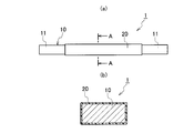
- FIG. 2A is a side view showing the conducting member according to this embodiment, and
- FIG. 2B is a cross-sectional view taken along the line AA in FIG.
- FIG. 3 is a schematic diagram showing various devices used in the method for manufacturing a conductive member according to the present embodiment.
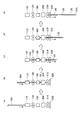
- FIG. 4 is a schematic diagram illustrating a method for manufacturing a conductive member according to the present embodiment (part 1).
- FIG. 5 is a schematic diagram illustrating a method for manufacturing a conductive member according to the present embodiment (part 2).
- FIG. 6 is a schematic view showing a method for manufacturing a conductive member according to another embodiment of the present invention.
- FIG. 7 is a cross-sectional view showing a conducting member according to a first conventional example.
- FIG. 1 is a perspective view showing a conducting member 1 according to the present embodiment.
- FIG. 2A is a side view showing the conducting member 1 according to this embodiment, and
- FIG. 2B is a cross-sectional view taken along the line AA in FIG.
- the conducting member 1 is preferably applied to a power supply circuit or the like in which insulation is a problem due to a relatively large voltage applied thereto, but can also be applied to other electric circuits that conduct current.
- the conductive member 1 includes a bus bar 10 and an insulating material 20 that covers each bus bar 10.
- bus bars 10 are arranged in the plate thickness direction. In the drawing, only one bus bar 10 is shown, and other bus bars 10 are omitted.
- the bus bar 10 is formed of a conductive material having a plate shape in cross section. Examples of the conductive material include copper, a copper alloy, and aluminum. At both ends of the bus bar 10, connection portions 11 connected to a power source such as a battery or various electric components are provided.
- the insulating material 20 is provided in the whole area except the connection part 11 among the bus bars 10.
- the insulating material 20 is formed of a resin that is cured by ultraviolet rays.
- a resin that is cured by ultraviolet rays.
- the insulating material 20 covers other than the connection portion 11 of the bus bar 10.
- the film thickness of the insulating material 20 is only required to ensure the insulating properties of the bus bar 10 and is appropriately determined according to the type of the insulating material 20 and is, for example, several ⁇ m to several hundred ⁇ m.
- the insulating material 20 is formed of a composite of epoxy acrylate, urethane acrylate, and acrylate monomer, and the film thickness is set to about 100 ⁇ m to 800 ⁇ m.
- FIG. 3 is a schematic diagram showing various devices used in the method for manufacturing the conductive member 1 according to the present embodiment.
- 4 and 5 are schematic views showing a method for manufacturing the conductive member 1 according to this embodiment.
- the method of manufacturing the conductive member 1 includes a step A in which a bus bar continuous body 10A in which the bus bar 10 is continuous in the longitudinal direction is formed by punching with a press, and an insulating material on the surface of the bus bar continuous body 10A (bus bar 10).
- Step B for applying
- step A a press device (not shown) for punching the conductive material to mold the bus bar continuous body 10A is used.
- a coating apparatus 100 that applies the insulating material 20 to the surface of the bus bar continuous body 10 ⁇ / b> A is used.
- step C as shown in FIGS. 3 and 4, an ultraviolet irradiation device 200 that irradiates the insulating material 20 with ultraviolet rays is used.
- a cutting device (not shown) for cutting the bus bar continuous body 10A is used.
- the bus bar continuous body 10 ⁇ / b> A formed from a conductive material by a press device is applied by a guide 110 or a roller 120. Guided to apparatus 100.
- the bus bar continuum 10 ⁇ / b> A is coated with the insulating material 20 on the surface by passing through the coating device 100.
- the insulating material 20 is sent from the tank 130 in which the insulating material 20 is stored by the liquid feed pump 140 every predetermined time.
- the power source of the liquid feed pump 140 is intermittently switched, or the inlet or outlet of the liquid feed pump 140 is intermittently connected by a shutter or the like. And the like that are obstructed.
- the insulating material 20 is applied to the bus bar continuous body 10A at predetermined intervals (so-called intermittent).
- the bus bar continuum 10 ⁇ / b> A to which the insulating material 20 is applied passes through the ultraviolet irradiation device 200, whereby the insulating material 20 is cured.
- the bus bar continuum 10 ⁇ / b> A having the cured insulating material 20 passes through the take-up roller 210, the wire diameter monitor 220, and the like.
- the cutting device (not shown) cuts the portion of the bus bar continuous body 10A where the insulating material 20 is not applied (that is, the connecting portion 11).
- the conductive member 1 is manufactured.
- the insulating material 20 is formed of a resin that is cured by ultraviolet rays. Thereby, there is no possibility that a void is generated unlike the conventional resin mold, and a predetermined insulating performance can be stably obtained according to the type and film thickness of the insulating material 20. Further, it can be manufactured with high productivity and at a low cost as compared with the case where a conventional insulating tape or the like is wound manually.
- the insulating material 20 can set the film thickness of the resin curable by ultraviolet rays, that is, the insulating material 20 to be thin. Therefore, the volume is smaller than that of a conventional resin cassette or resin mold, and it is not necessary to secure a creepage distance. Therefore, the arrangement space can be greatly reduced and the conductive member 1 can be reduced in weight.
- the bus bars 10 covered with the insulating material 20 can be integrally fixed by an adhesive means in a state where they are overlapped with each other, and the arrangement work for the electric circuit or the like is facilitated, and the space is reduced. It can be arranged compactly.
- the insulating material 20 is immediately cured by the ultraviolet irradiation device 200. Therefore, it can prevent that insulation performance falls, without the coating film of the edge part of the terminal of the insulating material 20 becoming thin.
- the insulating material 20 can be applied to the bus bar continuum 10A at predetermined intervals. Therefore, as compared with a method such as electrostatic powder coating, masking for not covering the connection portion 11 with the insulating material 20 is unnecessary, and the conductive member 1 can be formed continuously. Therefore, it is possible to reduce the manufacturing cost and the manufacturing time of the conductive member 1.
- the embodiment of the present invention can be modified as follows.
- the conductive member 1 is not limited to the manufacturing method described in the embodiment, and may be manufactured by other manufacturing methods.
- the conductive member 1 may be manufactured by a transparent mold 300 (upper mold 310 and lower mold 320).
- the insulating material 20 is cured by being irradiated with ultraviolet rays from the outside of the transparent mold 300.
- the bus bar continuous body 10 ⁇ / b> A is formed by being punched by a press.
- the present invention is not limited to this.
- the bus bar continuous body 10A may be molded by being applied.
- the shape of the bus bar 10 and the film thickness of the insulating material 20 are not limited to those described in the embodiment, and can be set as appropriate.
- the bus bar 10 has been described as being plate-shaped in cross section, but is not limited thereto, and may be circular or triangular in cross section.
- the insulating material 20 is provided so that the whole area
Landscapes
- Engineering & Computer Science (AREA)
- Manufacturing & Machinery (AREA)
- Chemical & Material Sciences (AREA)
- Chemical Kinetics & Catalysis (AREA)
- Electrochemistry (AREA)
- General Chemical & Material Sciences (AREA)
- Insulated Conductors (AREA)
- Battery Mounting, Suspending (AREA)
- Insulating Bodies (AREA)
- Connection Of Batteries Or Terminals (AREA)
Abstract
導通部材(1)は、板状の導電材からなるバスバー(10)と、バスバー(10)を被覆する絶縁材(20)とによって構成される。絶縁材(20)は、紫外線によって硬化する樹脂で形成される。
Description
本発明は、バッテリなどの電源に接続されて電気部品等に電気を供給する導通部材及び導通部材の製造方法に関する。
従来から、電源回路等には、バッテリなどの電源に接続されて電気部品等に電気を供給する導通部材(バスバーモジュールとも称する)が使用されている。この種の導通部材は、板状の導電材(例えば、銅や銅合金、アルミニウム)からなるバスバーを備える。バスバーは、その板厚方向に複数配設されている。各バスバーは、プレスによる打ち抜き加工が施されており、両端部にはそれぞれ接続部が設けられている。
導通部材は、省スペース化のためにできるだけ近接して配設することが望まれる一方、相互のバスバーの絶縁性を確保する必要がある。例えば、図7(a)~図7(d)に示すように、樹脂カセットや絶縁紙、絶縁テープ、樹脂モールドなどの絶縁材DによってバスバーBを絶縁する技術(以下、第1の従来例)が知られている(特許文献1参照)。また、バスバーBの周囲を絶縁材により塗装する技術(以下、第2の従来例)も知られている(特許文献2参照)。
しかしながら、上述した第1の従来例では、図7(a)に示すように、樹脂カセットによってバスバーBを絶縁する場合、バスバーBを挿入するための開口部Vを設ける必要がある。そのため、その開口部V側に所定の空間(沿面距離)を確保せざるを得なく、配設スペースが大きくなる。
また、図7(b)及び図7(c)に示すように、絶縁紙或いは絶縁テープによってバスバーBを絶縁する場合、当該絶縁紙或いは絶縁テープを作業者が装着したり巻き付けたりする必要がある。そのため、導通部材の製造が煩雑となることに伴い、導通部材の製造コストが増大してしまう。
また、図7(d)に示すように、樹脂モールドによってバスバーBを絶縁する場合、インサート成形する際にボイドが発生して絶縁性能が低下する恐れがあるとともに、金型費がかかってしまい、導通部材の製造コストが増大してしまう。
さらに、図7(a)及び図7(d)に示すように、樹脂カセットや樹脂モールドによってバスバーBを絶縁する場合、絶縁材Dの容積が大きいため、配設スペースが大きくなるとともに、導通部材の重量が増大してしまう。
また、上述した第2の従来例では、図示は省略しているが、塗装に使用する設備が大型化してしまうため、初期設備費用が増大してしまい、導通部材の製造コストが増大してしまう。
本発明は、絶縁性能を確保しつつ、軽量でかつ配設スペースを小さくでき、製造コストを低減できる導通部材及び導通部材の製造方法の提供を目的とする。
本発明の第1の態様は導通部材であって、導電材からなるバスバーと、紫外線によって硬化する樹脂で形成され、前記バスバーを被覆する絶縁材とを備えることを要旨とする。
本発明の第2の態様は、導電材からなるバスバーと、前記バスバーを被覆する絶縁材とによって構成される導通部材を製造する導通部材の製造方法であって、前記バスバーの表面に、紫外線によって硬化する樹脂で形成される絶縁材を塗布する工程と、前記バスバーの表面に塗布された前記絶縁材に紫外線を照射することによって前記絶縁材を硬化する工程とを含むことを要旨とする。
第2の態様に係る導通部材の製造方法は、前記絶縁材を塗布する工程の前に行われ、前記バスバーが長手方向に連続したバスバー連続体を成形する工程をさらに含んでもよい。前記絶縁材は、前記バスバー連続体に所定間隔おきに塗布されてもよい。
本発明によれば、絶縁性能を確保しつつ、軽量でかつ配設スペースを小さくでき、製造コストを低減できる導通部材及び導通部材の製造方法を提供することができる。
本発明の一実施形態に係る導通部材及び導通部材の製造方法について、図面を参照しながら説明する。以下の図面の記載において、同一または類似の部分には、同一または類似の符号を付している。ただし、図面は模式的なものであり、各寸法の比率などは現実のものとは異なることに留意すべきである。したがって、具体的な寸法などは以下の説明を参酌して判断すべきである。また、図面相互間においても互いの寸法の関係や比率が異なる部分が含まれ得る。
(導通部材の構成)
本実施形態に係る導通部材1の構成について、図面を参照しながら説明する。図1は、本実施形態に係る導通部材1を示す斜視図である。図2(a)は、本実施形態に係る導通部材1を示す側面図であり、図2(b)は、図2(a)のA-A断面図である。なお、導通部材1は、比較的大きな電圧が印加されて絶縁性が問題となる電源回路等に好適に適用されるが、電流を通電する他の電気回路にも適用され得る。
本実施形態に係る導通部材1の構成について、図面を参照しながら説明する。図1は、本実施形態に係る導通部材1を示す斜視図である。図2(a)は、本実施形態に係る導通部材1を示す側面図であり、図2(b)は、図2(a)のA-A断面図である。なお、導通部材1は、比較的大きな電圧が印加されて絶縁性が問題となる電源回路等に好適に適用されるが、電流を通電する他の電気回路にも適用され得る。
図1及び図2に示すように、導通部材1は、バスバー10と、各バスバー10を被覆する絶縁材20とによって構成される。
バスバー10は、その板厚方向に複数配設される。なお、図面では、バスバー10は、1個のみ記載されており、他のバスバー10が省略されている。バスバー10は、断面で板状からなる導電材によって形成される。この導電材としては、銅や銅合金、アルミニウムなどが挙げられる。バスバー10の両端には、バッテリなどの電源或いは各種電気部品等に接続される接続部11が設けられている。
絶縁材20は、バスバー10のうち接続部11を除く全域に設けられている。絶縁材20は、紫外線によって硬化する樹脂によって形成される。この樹脂としては、エポキシアクリレートやウレタンアクリレート、ポリエステルアクリレート、共重合系アクリレート、ポリブタジエンアクリレート、シリコンアクリレート、アミノ樹脂アクリレート、脂環式エポキシ樹脂、グリシジルエーテルエポキシ樹脂、ウレタンビニルエーテル、ポリエステルビニルエーテル、アクリレートモノマー、これらの複合材などが挙げられる。
絶縁材20は、バスバー10の接続部11以外を被覆している。絶縁材20の膜厚は、バスバー10の絶縁性を確保できればよく、絶縁材20の種類に応じて適宜定められ、例えば数μm~数百μmである。例えば、絶縁材20は、エポキシアクリレートやウレタンアクリレート、アクリレートモノマーの複合体によって形成されており、その膜厚は100μm~800μm程度に設定されている。
(導通部材の製造方法)
次に、上述した導通部材1の製造方法について、図面を参照しながら説明する。図3は、本実施形態に係る導通部材1の製造方法で使用される各種装置を示す模式図である。図4及び図5は、本実施形態に係る導通部材1の製造方法を示す模式図である。
次に、上述した導通部材1の製造方法について、図面を参照しながら説明する。図3は、本実施形態に係る導通部材1の製造方法で使用される各種装置を示す模式図である。図4及び図5は、本実施形態に係る導通部材1の製造方法を示す模式図である。
導通部材1の製造方法は、プレスによる打ち抜き加工が施されることによってバスバー10が長手方向に連続したバスバー連続体10Aを成型する工程Aと、バスバー連続体10A(バスバー10)の表面に絶縁材20を塗布する工程Bと、バスバー連続体10Aの表面に塗布された絶縁材20に紫外線を照射することによって絶縁材20を硬化する工程Cと、バスバー連続体10Aを切断してバスバー10を製造する工程Dとを含んでいる。
工程Aでは、導電材に打ち抜き加工を施してバスバー連続体10Aを成型するプレス装置(不図示)が使用される。工程Bでは、図3及び図4に示すように、バスバー連続体10Aの表面に絶縁材20を塗布する塗布装置100が使用される。工程Cでは、図3及び図4に示すように、絶縁材20に紫外線を照射する紫外線照射装置200が使用される。工程Dでは、バスバー連続体10Aを切断する切断装置(不図示)が使用される。
具体的には、図3、図4(a)及び図4(b)に示すように、プレス装置(不図示)により導電材から成型されたバスバー連続体10Aは、ガイド110やローラ120によって塗布装置100に案内される。そして、バスバー連続体10Aは、塗布装置100を通過することによって表面に絶縁材20を塗布される。
このとき、図3に示すように、絶縁材20が貯められたタンク130から液送ポンプ140によって絶縁材20を所定時間おきに送り込まれる。なお、液送ポンプ140から塗布装置100に絶縁材20を所定時間おき送り込む方法としては、液送ポンプ140の電源を断続的に切り替えることや、液送ポンプ140の入口又は出口をシャッターなどで断続的に閉塞するもの等が挙げられる。これにより、バスバー連続体10Aには、所定間隔おき(いわゆる、間欠的)に絶縁材20が塗布される。
次いで、図3、図4(b)及び図4(c)に示すように、絶縁材20が塗布されたバスバー連続体10Aは、紫外線照射装置200を通過することによって絶縁材20が硬化される。図3、図4(d)及び図4(e)に示すように、絶縁材20が硬化したバスバー連続体10Aは、引き取りローラ210や線径モニタ220等を通過する。その後、図5(a)~図5(c)に示すように、切断装置(不図示)によってバスバー連続体10Aにおける絶縁材20が塗布されていない部分(すなわち、接続部11)が切断されて、導通部材1が製造される。
(作用・効果)
以上説明した本実施形態では、絶縁材20は、紫外線によって硬化する樹脂で形成される。これにより、従来の樹脂モールドのようにボイドが生じる恐れがなく、絶縁材20の種類や膜厚に応じて所定の絶縁性能が安定して得られる。また、従来の絶縁テープなどを手作業で巻き付ける場合に比較して、高い生産性で安価に製造できる。
以上説明した本実施形態では、絶縁材20は、紫外線によって硬化する樹脂で形成される。これにより、従来の樹脂モールドのようにボイドが生じる恐れがなく、絶縁材20の種類や膜厚に応じて所定の絶縁性能が安定して得られる。また、従来の絶縁テープなどを手作業で巻き付ける場合に比較して、高い生産性で安価に製造できる。
本実施形態では、絶縁材20は、紫外線によって硬化する樹脂、すなわち、絶縁材20の膜厚を薄く設定できる。そのため、従来の樹脂カセットや樹脂モールドに比較して容積が小さくなり、沿面距離を確保する必要がない・従って、配設スペースを大幅に節減できるとともに、導通部材1の軽量化にも寄与する。
本実施形態では、絶縁材20で被覆されたバスバー10が互いに重ね合わされた状態で接着手段により一体的に固着することも可能となり、電気回路等に対する配設作業が容易になるとともに、小さなスペースにコンパクトに配設することができる。
本実施形態では、バスバー連続体10Aに絶縁材20が塗布された後、即座に絶縁材20が紫外線照射装置200によって硬化される。そのため、絶縁材20の端末のエッジ部分の塗膜が薄くなることなく、絶縁性能が低下してしまうことを防止できる。
加えて、バスバー連続体10Aに所定間隔おきに絶縁材20を塗布できる。そのため、静電粉体塗装等の工法と比較して、接続部11に絶縁材20を被覆しないためのマスキングが不要となり、導通部材1を連続的に形成できる。従って、導通部材1の製造コストの低減及び製造時間の短縮をも実現できる。
(その他の実施形態)
上述したように、本発明の実施形態を通じて本発明の内容を開示したが、この開示の一部をなす論述及び図面は、本発明を限定するものであると理解すべきではない。この開示から当業者には様々な代替実施の形態、実施例及び運用技術が明らかとなる。
上述したように、本発明の実施形態を通じて本発明の内容を開示したが、この開示の一部をなす論述及び図面は、本発明を限定するものであると理解すべきではない。この開示から当業者には様々な代替実施の形態、実施例及び運用技術が明らかとなる。
例えば、本発明の実施形態は、次のように変更することができる。具体的には、導通部材1は、実施形態で説明した製造方法に限定されるものではなく、その他の製造方法によって製造されてもよい。例えば、図6に示すように、導通部材1は、透明金型300(上側金型310及び下側金型320)によって製造されてもよい。このとき、絶縁材20は、透明金型300の外部から紫外線が照射されることによって硬化される。
また、導通部材1の製造方法における工程Aでは、プレスによる打ち抜き加工が施されることによってバスバー連続体10Aを成型するものとして説明したが、これに限定されるものではなく、例えば、スリット加工が施されることによってバスバー連続体10Aを成型するものであってもよい。
また、バスバー10の形状や絶縁材20の膜厚などについては、実施形態で説明したものに限定されるものではなく、適宜設定できることは勿論である。例えば、バスバー10は、断面で板状であるとして説明したが、これに限定されるものではなく、断面で円形状や三角状であってもよい。
また、絶縁材20は、バスバー10の表面のうち接続部11を除く全域を被覆するように設けられるが、これに限定されるものではなく、絶縁性能が問題にならない部分については必ずしも絶縁材20で被覆する必要はない。
このように、本発明は、ここでは記載していない様々な実施の形態などを含むことは勿論である。したがって、本発明の技術的範囲は、上述の説明から妥当な特許請求の範囲に係る発明特定事項によってのみ定められる。
Claims (3)
- 導通部材であって、
導電材からなるバスバーと、
紫外線によって硬化する樹脂で形成され、前記バスバーを被覆する絶縁材とを備えることを特徴とする導通部材。 - 導電材からなるバスバーと、前記バスバーを被覆する絶縁材とによって構成される導通部材を製造する導通部材の製造方法であって、
前記バスバーの表面に、紫外線によって硬化する樹脂で形成される前記絶縁材を塗布する工程と、
前記バスバーの表面に塗布された前記絶縁材に紫外線を照射することによって前記絶縁材を硬化する工程とを含むことを特徴とする導通部材の製造方法。 - 請求項2に記載の導通部材の製造方法であって、
前記絶縁材を塗布する工程の前に行われ、前記バスバーが長手方向に連続したバスバー連続体を成形する工程をさらに含み、
前記絶縁材を塗布する工程では、前記バスバー連続体に所定間隔おきに前記絶縁材を塗布することを特徴とする導通部材の製造方法。
Priority Applications (3)
| Application Number | Priority Date | Filing Date | Title |
|---|---|---|---|
| DE112013005709.3T DE112013005709T5 (de) | 2012-11-29 | 2013-11-01 | Leitfähiges Element und Leitfähiges-Element-Herstellungsverfahren |
| CN201380062131.6A CN104813416A (zh) | 2012-11-29 | 2013-11-01 | 导电部件,以及导电部件制造方法 |
| US14/723,600 US20150279520A1 (en) | 2012-11-29 | 2015-05-28 | Conductive member, and conductive member manufacturing method |
Applications Claiming Priority (2)
| Application Number | Priority Date | Filing Date | Title |
|---|---|---|---|
| JP2012-260898 | 2012-11-29 | ||
| JP2012260898A JP2014107201A (ja) | 2012-11-29 | 2012-11-29 | 導通部材及び導通部材の製造方法 |
Related Child Applications (1)
| Application Number | Title | Priority Date | Filing Date |
|---|---|---|---|
| US14/723,600 Continuation US20150279520A1 (en) | 2012-11-29 | 2015-05-28 | Conductive member, and conductive member manufacturing method |
Publications (1)
| Publication Number | Publication Date |
|---|---|
| WO2014084003A1 true WO2014084003A1 (ja) | 2014-06-05 |
Family
ID=50827649
Family Applications (1)
| Application Number | Title | Priority Date | Filing Date |
|---|---|---|---|
| PCT/JP2013/079763 Ceased WO2014084003A1 (ja) | 2012-11-29 | 2013-11-01 | 導通部材及び導通部材の製造方法 |
Country Status (5)
| Country | Link |
|---|---|
| US (1) | US20150279520A1 (ja) |
| JP (1) | JP2014107201A (ja) |
| CN (1) | CN104813416A (ja) |
| DE (1) | DE112013005709T5 (ja) |
| WO (1) | WO2014084003A1 (ja) |
Cited By (1)
| Publication number | Priority date | Publication date | Assignee | Title |
|---|---|---|---|---|
| CN110311083A (zh) * | 2019-07-24 | 2019-10-08 | 宁波市叶兴汽车零部件有限公司 | 车用电池连接件加工工艺 |
Families Citing this family (22)
| Publication number | Priority date | Publication date | Assignee | Title |
|---|---|---|---|---|
| JP2016066435A (ja) | 2014-09-24 | 2016-04-28 | 矢崎総業株式会社 | バスバー及びバスバーの製造方法 |
| JP2016081732A (ja) * | 2014-10-17 | 2016-05-16 | 矢崎総業株式会社 | 電線及び電線の製造方法 |
| JP2016081731A (ja) * | 2014-10-17 | 2016-05-16 | 矢崎総業株式会社 | 平角電線及び平角電線の製造方法 |
| JP2016085822A (ja) * | 2014-10-24 | 2016-05-19 | 矢崎総業株式会社 | 導通部材の製造方法、ワイヤハーネスおよびその製造方法 |
| JP6350309B2 (ja) * | 2015-01-28 | 2018-07-04 | アイシン・エィ・ダブリュ株式会社 | 平角線の製造方法及び回転電機用ステータの製造方法 |
| JP6592284B2 (ja) * | 2015-06-18 | 2019-10-16 | 矢崎総業株式会社 | 給電リング及び給電リングの製造方法 |
| JP6592285B2 (ja) * | 2015-06-18 | 2019-10-16 | 矢崎総業株式会社 | 給電リング |
| JP6585395B2 (ja) * | 2015-06-18 | 2019-10-02 | 矢崎総業株式会社 | 給電リング及び給電リングの製造方法 |
| CN105098106A (zh) * | 2015-08-31 | 2015-11-25 | 王新峰 | 电池的金属外壳结构及其绝缘处理方法 |
| JP6290165B2 (ja) | 2015-12-18 | 2018-03-07 | 矢崎総業株式会社 | バスバーモジュールの製造方法及び電池パックの製造方法 |
| JP6298842B2 (ja) * | 2016-03-10 | 2018-03-20 | 株式会社オートネットワーク技術研究所 | 接続モジュール |
| US11189887B2 (en) | 2017-03-16 | 2021-11-30 | Ford Global Technologies, Llc | Busbar assembly for an electrified vehicle and method of forming the same |
| JP6637002B2 (ja) * | 2017-09-04 | 2020-01-29 | サンコール株式会社 | バスバーアッセンブリの製造方法 |
| JP7006051B2 (ja) * | 2017-09-08 | 2022-02-10 | 日産自動車株式会社 | 電池パック、導電部材および保護部材 |
| CN109637751B (zh) * | 2017-10-06 | 2022-07-29 | 力特有限公司 | 用于制造被绝缘的汇流条的方法 |
| US11508495B2 (en) * | 2017-12-14 | 2022-11-22 | Schneider Electric USA, Inc. | Method of preparing epoxy coated bus bars for use in electrical distribution equipment |
| JP6820292B2 (ja) | 2018-06-19 | 2021-01-27 | 矢崎総業株式会社 | 導通部材 |
| KR102819127B1 (ko) | 2020-03-31 | 2025-06-12 | 주식회사 엘지에너지솔루션 | 이종금속으로 이루어진 hv 버스 바 및 이의 제조 방법 |
| JP7123514B2 (ja) * | 2020-06-17 | 2022-08-23 | 矢崎総業株式会社 | 導電構造体 |
| JP7663013B2 (ja) * | 2021-04-23 | 2025-04-16 | 株式会社オートネットワーク技術研究所 | バスバー部材の製造方法 |
| JP7518133B2 (ja) * | 2022-07-29 | 2024-07-17 | イビデン株式会社 | バスバー及びその製造方法、並びに蓄電装置 |
| KR20240059428A (ko) * | 2022-10-27 | 2024-05-07 | 주식회사 엘지에너지솔루션 | 버스바를 일체로 구비하는 단자 구조체 어셈블리 |
Citations (3)
| Publication number | Priority date | Publication date | Assignee | Title |
|---|---|---|---|---|
| JPH0274113A (ja) * | 1988-09-07 | 1990-03-14 | Yazaki Corp | ブスバー回路板の製造方法 |
| JP2005251673A (ja) * | 2004-03-08 | 2005-09-15 | Toyota Motor Corp | バスバー製造方法、バスバー |
| JP2008270290A (ja) * | 2007-04-16 | 2008-11-06 | Sumitomo Electric Ind Ltd | パワーモジュール、その製造方法および素子接続用バスバー |
Family Cites Families (4)
| Publication number | Priority date | Publication date | Assignee | Title |
|---|---|---|---|---|
| JPS5426496B1 (ja) * | 1968-11-02 | 1979-09-04 | ||
| JP2660680B2 (ja) * | 1995-05-09 | 1997-10-08 | 智 小野寺 | 導体のラッピング接続法とラッピング用具 |
| JP4506818B2 (ja) * | 2007-11-15 | 2010-07-21 | 住友電気工業株式会社 | シールドフラットケーブルの製造方法 |
| CN101451257A (zh) * | 2007-11-29 | 2009-06-10 | 住友电气工业株式会社 | 扁平电缆的电镀方法及包含该方法的扁平电缆制造方法 |
-
2012
- 2012-11-29 JP JP2012260898A patent/JP2014107201A/ja not_active Abandoned
-
2013
- 2013-11-01 CN CN201380062131.6A patent/CN104813416A/zh active Pending
- 2013-11-01 WO PCT/JP2013/079763 patent/WO2014084003A1/ja not_active Ceased
- 2013-11-01 DE DE112013005709.3T patent/DE112013005709T5/de not_active Withdrawn
-
2015
- 2015-05-28 US US14/723,600 patent/US20150279520A1/en not_active Abandoned
Patent Citations (3)
| Publication number | Priority date | Publication date | Assignee | Title |
|---|---|---|---|---|
| JPH0274113A (ja) * | 1988-09-07 | 1990-03-14 | Yazaki Corp | ブスバー回路板の製造方法 |
| JP2005251673A (ja) * | 2004-03-08 | 2005-09-15 | Toyota Motor Corp | バスバー製造方法、バスバー |
| JP2008270290A (ja) * | 2007-04-16 | 2008-11-06 | Sumitomo Electric Ind Ltd | パワーモジュール、その製造方法および素子接続用バスバー |
Cited By (1)
| Publication number | Priority date | Publication date | Assignee | Title |
|---|---|---|---|---|
| CN110311083A (zh) * | 2019-07-24 | 2019-10-08 | 宁波市叶兴汽车零部件有限公司 | 车用电池连接件加工工艺 |
Also Published As
| Publication number | Publication date |
|---|---|
| US20150279520A1 (en) | 2015-10-01 |
| DE112013005709T5 (de) | 2015-09-10 |
| JP2014107201A (ja) | 2014-06-09 |
| CN104813416A (zh) | 2015-07-29 |
Similar Documents
| Publication | Publication Date | Title |
|---|---|---|
| JP2014107201A (ja) | 導通部材及び導通部材の製造方法 | |
| CN109643940B (zh) | 层叠铁芯、层叠铁芯的制造方法及使用层叠铁芯的电枢 | |
| EP2683040A1 (en) | Bus-bar set and manufacturing method therefor | |
| JP2016081731A (ja) | 平角電線及び平角電線の製造方法 | |
| US10553331B2 (en) | Edge insulation structure for electrical cable | |
| CN106463249B (zh) | 电抗器 | |
| US11128191B2 (en) | Wire bonding device of stator of motor | |
| US20150022045A1 (en) | Electrical Rotating Machine | |
| EP3611827A1 (en) | Coil and motor using same | |
| CN102725931A (zh) | 配电安装部件及使用配电安装部件的逆变器装置 | |
| CN103384955A (zh) | 旋转电机的定子及其制造方法 | |
| JP4992767B2 (ja) | コンデンサ装置。 | |
| US10715031B2 (en) | Power converter | |
| JP2013187004A (ja) | コネクタ付電線 | |
| KR20170090157A (ko) | 이차전지용 파우치필름을 제조하기 위한 복합 라미네이션 장치 | |
| JP6175043B2 (ja) | 印刷回路体 | |
| WO2016047634A1 (ja) | バスバー及びバスバーの製造方法 | |
| JP6973341B2 (ja) | ワイヤハーネス | |
| US20170103831A1 (en) | Methods for Manufacturing an Insulated Busbar | |
| CN106876644A (zh) | 一种电连接板 | |
| EP3608923B1 (en) | Apparatus and method for applying an insulation material onto a conductor | |
| JP2000215735A (ja) | 積層バスバ― | |
| JP2006024449A (ja) | バスバーおよび通電装置 | |
| JP2014229659A (ja) | インダクタとその製造方法 | |
| JP2016085822A (ja) | 導通部材の製造方法、ワイヤハーネスおよびその製造方法 |
Legal Events
| Date | Code | Title | Description |
|---|---|---|---|
| 121 | Ep: the epo has been informed by wipo that ep was designated in this application |
Ref document number: 13858637 Country of ref document: EP Kind code of ref document: A1 |
|
| WWE | Wipo information: entry into national phase |
Ref document number: 1120130057093 Country of ref document: DE Ref document number: 112013005709 Country of ref document: DE |
|
| 122 | Ep: pct application non-entry in european phase |
Ref document number: 13858637 Country of ref document: EP Kind code of ref document: A1 |