WO2014080688A1 - 静電チャック及び給電システム - Google Patents
静電チャック及び給電システム Download PDFInfo
- Publication number
- WO2014080688A1 WO2014080688A1 PCT/JP2013/075602 JP2013075602W WO2014080688A1 WO 2014080688 A1 WO2014080688 A1 WO 2014080688A1 JP 2013075602 W JP2013075602 W JP 2013075602W WO 2014080688 A1 WO2014080688 A1 WO 2014080688A1
- Authority
- WO
- WIPO (PCT)
- Prior art keywords
- electrostatic chuck
- low voltage
- booster circuit
- vacuum chamber
- electrode
- Prior art date
- Legal status (The legal status is an assumption and is not a legal conclusion. Google has not performed a legal analysis and makes no representation as to the accuracy of the status listed.)
- Ceased
Links
Images




Classifications
-
- H—ELECTRICITY
- H02—GENERATION; CONVERSION OR DISTRIBUTION OF ELECTRIC POWER
- H02N—ELECTRIC MACHINES NOT OTHERWISE PROVIDED FOR
- H02N13/00—Clutches or holding devices using electrostatic attraction, e.g. using Johnson-Rahbek effect
-
- H—ELECTRICITY
- H10—SEMICONDUCTOR DEVICES; ELECTRIC SOLID-STATE DEVICES NOT OTHERWISE PROVIDED FOR
- H10P—GENERIC PROCESSES OR APPARATUS FOR THE MANUFACTURE OR TREATMENT OF DEVICES COVERED BY CLASS H10
- H10P72/00—Handling or holding of wafers, substrates or devices during manufacture or treatment thereof
- H10P72/70—Handling or holding of wafers, substrates or devices during manufacture or treatment thereof for supporting or gripping
- H10P72/72—Handling or holding of wafers, substrates or devices during manufacture or treatment thereof for supporting or gripping using electrostatic chucks
- H10P72/722—Details of electrostatic chucks
Definitions
- the present invention relates to an electrostatic chuck and a power feeding system for adsorbing a workpiece such as a glass substrate.
- the electrostatic chuck 100 is normally fixed to the bottom of the vacuum chamber 200 of the processing apparatus. Then, a driving power supply voltage or an electric signal is supplied from the power supply 210 outside the vacuum chamber 200 to the electrostatic chuck 100, and the workpiece plate W is attracted to the electrostatic chuck 100 (see, for example, Patent Document 1). .
- the processed plate body W cannot be moved to a predetermined position in the apparatus 200 or the processed plate body W cannot be reversed. The adaptability to processing work was poor.
- the electrostatic chuck 100 is movably installed in the vacuum chamber 200 of the processing apparatus. As shown in FIG. 9, the electrostatic chuck 100 is slidably disposed on a stage 150. As a result, the electrostatic chuck 100 is conveyed to a predetermined location in the vacuum chamber 200 with the workpiece W being sucked, and the workpiece plate W is arranged at that location.
- the power source 210 is disposed outside the vacuum chamber 200, and the power source 210 and the power supply pins 131 and 131 extending from the adsorption electrode 130 are connected through the voltage cables 220 and 220. .
- the inside of the vacuum chamber 200 is in a vacuum atmosphere, and there is a high possibility that discharge will occur between the voltage cables 220 and 220. For this reason, high voltage cables are used as the voltage cables 220 and 220, and discharge in the cable portion in the apparatus 200 is prevented in consideration of Paschen's easy discharge region. This is achieved by sealing the portion where the conductor portion tends to be exposed with silicone or epoxy rubber resin. Specifically, the connection portions between the in-device cable portions 221 and 221 of the voltage cables 220 and 220 and the feeding pins 131 and 131 are sealed with the sealing materials 231 and 231, and the in-device cable portions 221 and 221 and the device are connected. Connection portions with the outer cable portions 222 and 222 are sealed with sealing materials 232 and 232.
- the conventional techniques described above have the following problems. That is, by repeating the movement of the electrostatic chuck 100 for many years, the connection portions between the in-device cable portions 221 and 221 and the power supply pins 131 and 131 and the connection between the in-device cable portions 221 and 221 and the external cable portions 222 and 222 are connected. A load may be applied to the portion, and the sealing materials 231 and 232 may be deteriorated. As a result, these connecting portions are exposed, which may cause discharge. Further, since it is necessary to arrange the long cable portions 221 and 221 in the vacuum chamber 200, to provide cable piping, and to provide the sealing materials 231 and 232, the structure of the power feeding system to the electrostatic chuck becomes complicated.
- the present invention has been made to solve the above-described problems, and enables high-voltage driving without generating a discharge even in a vacuum atmosphere, and simplifies the structure of a power feeding system to an electrostatic chuck. It is an object of the present invention to provide an electrostatic chuck and a power feeding system that can be realized.
- the invention of claim 1 is directed to a dielectric having a surface having an adsorption surface of a plate to be processed, an electrostatic adsorption layer having an adsorption electrode disposed inside the dielectric, A substrate having an adsorption layer disposed on the upper surface, a low voltage input terminal for inputting a low voltage from an external power source, and a high voltage for supplying a high voltage obtained by boosting the low voltage to the adsorption electrode
- An electrostatic chuck including a booster circuit having a voltage output terminal, the end of the wiring that is attached to the base material and is pulled out from the adsorption electrode through the dielectric body and the base material in an unexposed state And the high voltage output terminal are placed in a base material in a non-exposed state.
- the electrostatic chuck when the electrostatic chuck is arranged in the vacuum chamber and a low voltage is sent from the external power supply outside the vacuum chamber to the electrostatic chuck side, the low voltage is input to the booster circuit through the low voltage input terminal. . Then, this low voltage is boosted to a high voltage by the boosting circuit, and the high voltage is output from the high voltage output terminal to the suction electrode, and an electrostatic force is generated on the workpiece plate and the electrostatic suction layer surface. Thereby, a to-be-processed board body is adsorb
- the low voltage from the external power source is input from the external power source to the low voltage input terminal of the booster circuit through the cable introduced into the vacuum chamber. Accordingly, since a low voltage is supplied from the cable to the booster circuit, no discharge occurs in the cable itself. Further, even when the connection portion between the cable and the low voltage input terminal is exposed, no discharge occurs. However, since a high voltage is supplied between the high voltage output terminal of the booster circuit and the adsorption electrode, the discharge is caused by the wiring itself between the booster circuit and the adsorption electrode, or the high voltage output terminal and the wiring end. There is a possibility that it may occur at the connection part with the part.
- the wiring passes from the attracting electrode through the dielectric and the base material, and the electrical connection portion between the end of the wiring and the high voltage output terminal is accommodated in the base material. Therefore, even if a high voltage is supplied between the high voltage output terminal and the adsorption electrode of the booster circuit, the discharge is not generated in the wiring itself or the high voltage output terminal and the wiring end. There is no possibility that it will occur in the connection part.
- the low voltage input terminal of the booster circuit inputs a voltage within the range of 5 to 100 volts, and the high voltage output terminal is 300 volts.
- the voltage output is in the range of volt to 10,000 volts.
- a power feeding system in which the electrostatic chuck according to the first or second aspect and a fixed electrode fixed in the vacuum chamber are connected to an external power source.
- the movable electrode that moves together with the electrostatic chuck is connected to the low voltage input terminal of the booster circuit, and the low voltage from the external power source is applied to the low voltage input terminal of the booster circuit by the contact between the fixed electrode and the movable electrode.
- An input electrical contact mechanism is provided.
- the length of the cable is sufficient up to the fixed electrode and should be very short. Can do.
- a low voltage is supplied to the cable, it is not necessary to seal the connection portion between the cable and the fixed electrode.
- the fixed electrode of the electrical contact mechanism is formed of a conductive rail disposed in parallel to the transport direction in the state of being close to the electrostatic chuck.
- the movable electrode is formed of a conductive flexible contact attached to the electrostatic chuck in contact with the rail.
- the transport mechanism includes a plurality of conductive rollers arranged in the transport direction and a pair of parallel lanes that rotatably support these rollers.
- the fixed electrode of the electrical contact mechanism is formed of a plurality of conductive rollers
- the movable electrode is formed of an electrode plate that moves together with the electrostatic chuck in contact with the rollers.
- a power feeding system in which the electrostatic chuck according to the first or second aspect and a stationary coil fixed in the vacuum chamber are connected to an external power source.
- a movable coil that moves together with the electrostatic chuck in a non-contact state with the fixed coil is connected to the low voltage input terminal of the booster circuit, and a low voltage from an external power source is reduced by electromagnetic induction from the fixed coil to the movable coil.
- an electromagnetic induction device for inputting to the low voltage input terminal of the booster circuit.
- a low voltage is generated in the movable coil by electromagnetic induction from the fixed coil to the movable coil, and is input to the low voltage input terminal of the booster circuit.
- the high voltage boosted by the booster circuit is supplied to the adsorption electrode through the high voltage output terminal and the wiring. That is, during the conveyance of the electrostatic chuck, the low voltage from the external power source continues to be supplied to the low voltage input terminal of the booster circuit through the electrically non-contact electromagnetic induction device.
- the fixed coil of the electromagnetic induction device is fixed in the vacuum chamber, and the movable coil is attached to the electrostatic chuck.
- a power feeding system according to the first or second aspect, wherein the power supply system is transported by a transport mechanism in the vacuum chamber, and at least an upper surface of the vacuum chamber. And a solar cell that converts light introduced into the vacuum chamber through the transparent top plate into low voltage electricity and inputs it to the low voltage input terminal of the booster circuit of the electrostatic chuck And a device.
- the converted low voltage is input to the low voltage input terminal of the booster circuit, and the high voltage boosted by the booster circuit is supplied to the adsorption electrode through the high voltage output terminal and the wiring. That is, during the conveyance of the electrostatic chuck, the electrostatic chuck is continuously driven by the light from the external light source.
- the invention of claim 9 is the power supply system according to claim 8, wherein the solar cell device is attached to the electrostatic chuck.
- the electrostatic chuck of the invention of claim 1 and claim 2 in the vacuum chamber, only the low voltage supply portion between the external power supply and the booster circuit is exposed,
- the high voltage supply part such as the wiring itself between the booster circuit and the adsorption electrode and the connection part between the high voltage output terminal and the wiring end is configured to be in an unexposed state.
- the electrical breakdown mode arcing
- the breakdown of the insulating part due to the drive can be avoided. That is, according to the present invention, there is an excellent effect of enabling high voltage driving without generating discharge even in a vacuum atmosphere.
- the cable from the external power source is connected to the fixed electrode fixed in the vacuum chamber, the cable length is up to the fixed electrode.
- the length is sufficient and can be very short.
- a low voltage is supplied to the cable, it is not necessary to seal the connection portion between the cable and the fixed electrode. Therefore, it is possible to reduce the cable disadvantageous to the vacuum atmosphere, the piping for the cable, the sealing mechanism, and the like. As a result, the structure of the power feeding system to the electrostatic chuck can be simplified. effective.
- the low voltage from the external power source passes through the electrically non-contact electromagnetic induction device and the low voltage of the booster circuit. Therefore, the effect of preventing discharge in a vacuum atmosphere can be further enhanced.
- the electrostatic chuck is continuously driven by the light from the external light source during the conveyance of the electrostatic chuck.
- Cable, piping, etc. can be eliminated completely, and as a result, there is an excellent effect that the structure of the power feeding system can be further simplified.
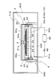
- FIG. 1 is a schematic sectional view showing an electrostatic chuck and a power feeding system according to a first embodiment of the present invention.
- a power supply system 1-1 exemplified in this embodiment is a system for supplying an external power source to an electrostatic chuck 2 in a vacuum chamber 200 of a vapor deposition apparatus, and is transported by a transport mechanism 300.
- the electrostatic chuck 2 and the electrical contact mechanism 4 are provided.
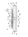
- FIG. 2 is a cross-sectional view showing the electrostatic chuck 2.
- the electrostatic chuck 2 includes a base material 20, an electrostatic adsorption layer 21, and a booster circuit 3.
- the substrate 20 is made of aluminum, SUS, iron, copper, titanium, ceramic (including ALN, SiC, Al2O3, SiN, zirconia, BN, TiC, TiN), etc. It is affixed on the base material 20.
- the electrostatic adsorption layer 21 includes a dielectric 22 and an adsorption electrode 23, and the surface 21 a is an adsorption surface of a plate W to be processed such as a glass substrate.
- the dielectric 22 is made of a polyimide film or ceramic.
- the adsorption electrode 23 is made of a conductive material (foil or paste) containing carbon ink, Cu, SUS, iron, nickel, silver, platinum, or the like as a main component or mixed therein, and is boosted through wirings 24 and 25. It is electrically connected to the circuit 3.
- the booster circuit 3 is a device that boosts a low voltage input from the low voltage input terminals 31a and 32a to a high voltage and outputs the boosted voltage from the high voltage output terminals 31b and 32b, for example, a DC-DC converter, an AC-DC, and the like. Converter or AC-AC converter.
- Such a booster circuit 3 is mounted in a state of being embedded in the base material 20. Specifically, the low voltage input terminals 31 a and 32 a are exposed to the outside, and the high voltage output terminals 31 b and 32 b are accommodated in the base material 20.
- the high voltage output terminals 31b and 32b are connected to the ends of the wirings 24 and 25 drawn from the adsorption electrode 23 through the dielectric 22 and the base material 20, and these electrical connection portions P1. , P2 are in an unexposed state.
- FIG. 3 is a schematic plan view showing the power feeding system 1-1.
- the transport mechanism 300 includes a pair of lanes 301 and 302, a plurality of pairs of rollers 311 and 312 that are rotatably supported by the lanes 301 and 302, and rollers 311 and 312. And a drive mechanism (not shown) for driving and rotating the motor.
- the vapor deposition material 230a needs to be sprayed from the vapor deposition source 230 on the floor of the vacuum chamber 200 to the upper plate W to be processed to deposit the plate W to be processed.
- the electrostatic chuck 2 is placed on the rollers 311 and 312 of the transport mechanism 300 in a state of being directed downward. Specifically, the electrostatic chuck 2 on which the mask 5 is placed on the rollers 311 and 312 and attracts the processed plate body W is assembled on the mask 5 with the processed plate body W facing downward. ing. Thereby, the vapor deposition material 230a sprayed from the lower vapor deposition source 230 is vapor-deposited on the surface of the plate W to be processed in a shape corresponding to the pattern of the mask 5.
- the electrical contact mechanism 4 is a mechanism for inputting a low voltage from the external power supply 40 to the low voltage input terminals 31 a and 32 a of the booster circuit 3.
- the electrical contact mechanism 4 includes conductive rails 41 and 42 as fixed electrodes and conductive flexible contacts 43 and 44 as movable electrodes.
- the rails 41 and 42 are disposed in parallel with the transport direction (the front and back direction in FIG. 1, the up and down direction in FIG. 3) in the state of being close to the electrostatic chuck 2, and are fixed in the vacuum chamber 200. ing.
- the rail 41 is connected to one terminal of the external power supply 40 through the cable 41a, and the rail 42 is connected to the other terminal of the external power supply 40 through the cable 42a. As shown in FIG.
- the conductive plate 45 is attached to the left side surface of the substrate 20 of the electrostatic chuck 2 via an insulating film (not shown), and the flexible contact 43 is connected to the conductive plate 45. There are several plants in the area.
- a conductive plate 46 is attached to the right side surface of the substrate 20 via an insulating film (not shown), and a plurality of flexible contacts 44 are implanted in the conductive plate 46. As shown in FIG. 1, the tip portions of the flexible contacts 43 and 44 are in pressure contact with the rails 41 and 42, respectively. The flexible contacts 43 and 44 are in contact with the rails 41 and 42. In the state, it moves together with the electrostatic chuck 2 in the transport direction.
- the conductive plate 45 in which the flexible contact 43 is implanted is connected to the low voltage input terminal 31a of the booster circuit 3 through the cable 45a, and the conductive plate 46 in which the flexible contact 44 is implanted is The low voltage input terminal 32a of the booster circuit 3 is connected through the cable 46a.
- the external power supply 40 is connected to the low voltage input terminals 31a and 32a of the booster circuit 3 through the contact between the rails 41 and 42 and the flexible contacts 43 and 44, and the high voltage of the booster circuit 3 is connected.
- the output terminals 31b and 32b are connected to the suction electrode 23 through wirings 24 and 25.
- the low voltage from the external power supply 40 can be set to a voltage in the range of 5 volts to 100 volts
- the high voltage from the booster circuit 3 can be set to a voltage in the range of 300 volts to 10000 volts.
- +24 volts was applied to the low voltage input terminal 31a of the booster circuit 3, and the low voltage input terminal 32a was grounded.
- +2000 volts and -2000 volts were output from the high voltage output terminals 31b and 32b, respectively, and a high voltage of 4000 volts was applied to the adsorption electrode 23.
- FIG. 1 when the switch 49 is closed, the low voltage +24 volts from the external power supply 40 is applied to the low voltage input terminals 31a and 32a of the booster circuit 3 through the cables 41a and 42a, the electrical contact mechanism 4 and the cables 45a and 46a. Entered. Then, high voltages +2000 volts and ⁇ 2000 volts are output from the high voltage output terminals 31 b and 32 b of the booster circuit 3, and a high voltage of 4000 volts is applied to the adsorption electrode 23 through the wirings 24 and 25.
- the discharge is caused by the wiring 24 between the booster circuit 3 and the suction electrode 23. , 25 itself, and connection portions P1, P2 between the high voltage output terminals 31b, 32b and the ends of the wirings 24, 25.
- the wires 24 and 25 are drawn from the attracting electrode 23 through the dielectric 22 and the base material 20 in an unexposed state, and the ends of the wires 24 and 25 and the high voltage are used. Electrical connection portions P1 and P2 with the output terminals 31b and 32b are housed in the base material 20 and are not exposed.
- the vapor deposition material 230a is passed when the workpiece plate W passes just above the vapor deposition source 230. Is sprayed, and the vapor deposition process to the workpiece plate W is executed.
- the flexible contacts 43 and 44 of the electrical contact mechanism 4 are kept in contact with the rails 41 and 42 even when the electrostatic chuck 2 is being transported, the low voltage +24 from the external power source 40 can be obtained.
- FIG. 4 is a sectional view showing a power feeding system according to a second embodiment of the present invention
- FIG. 5 is a schematic plan view showing the power feeding system.
- the structure of the electric contact mechanism is different from that of the electric contact mechanism 4 of the power supply system 1-1 of the first embodiment.
- reference numeral 6 denotes an electrical contact mechanism, and the electrical contact mechanism 6 has a structure using a roller of the transport mechanism 300.
- a plurality of pairs of rollers 311 and 312 (see FIG. 1) of the transport mechanism 300 in the first embodiment are formed by conductive rollers 61 and 62, and these rollers 61 and 62 are electrically contacted. 6 fixed electrodes.
- the rollers 61 and 62 were connected to both terminals of the external power supply 40 through cables 61a and 62a, respectively. As shown in FIG. 5, these rollers 61 and 62 are attached to both ends of each roller 6a-1 (6a-2 to 6a-10), and a plurality of rollers 6a-1 to 6a-10 are connected to the lane 301, 302 is rotatably attached.
- both terminals of the external power supply 40 are connected to the rollers 61 and 62 of all the rollers 6a-1 to 6a-10.
- the low voltage of the external power supply 40 is supplied only to the rollers 61 and 62 of the rollers 6a-1 to 6a-6 in a certain area, or, for example, every third roller 6a-1, 6a-4, A low voltage may be supplied only to the rollers 61 and 62 of 6a-7 and 6a-10.
- the movable electrode of the electrical contact mechanism 6 was formed by electrode plates 63 and 64 attached to the mask 5 as shown in FIG. These electrode plates 63 and 64 were brought into contact with the rollers 61 and 62 and connected to the low voltage input terminals 31a and 32a of the booster circuit 3 through the cables 63a and 64a.
- the electrode plates 63 and 64 attached to the mask 5 move together with the electrostatic chuck 2.
- the low voltage +24 volts from the external power supply 40 is electrically The voltage is input to the low voltage input terminals 31 a and 32 a of the booster circuit 3 through the contact mechanism 6.
- the high voltages +2000 volts and ⁇ 2000 volts boosted by the booster circuit 3 are supplied to the adsorption electrode 23 through the wirings 24 and 25. Since other configurations, operations, and effects are the same as those in the first embodiment, description thereof is omitted.
- FIG. 6 is a schematic plan view showing a power feeding system according to the third embodiment of the present invention.
- the power supply system 1-3 of this embodiment is different from the power supply systems of the first and second embodiments in that an electromagnetic induction device is provided instead of the electrical contact mechanism of the above embodiment.
- symbol 7 is an electromagnetic induction apparatus.
- the electromagnetic induction device 7 includes a fixed coil 71 fixed in the vacuum chamber 200 and a movable coil 72 attached to the electrostatic chuck 2.
- the length of the fixed coil 71 is set substantially equal to the conveyance range of the electrostatic chuck 2, and both ends thereof are connected to both terminals of the external power supply 40 through cables 71 a and 71 b.
- the external power supply 40 inputs an alternating low voltage to the fixed coil 71.
- the movable coil 72 is attached on the base material 20 of the electrostatic chuck 2 in a state close to the fixed coil 71, and both ends thereof are connected to the low voltage input terminals 31 a and 32 a of the booster circuit 3.
- the movable coil 72 moves together with the electrostatic chuck 2 in a non-contact state with the fixed coil 71.
- a low voltage alternating current is input from the external power supply 40 to the fixed coil 71
- the voltage induced by electromagnetic induction from the fixed coil 71 to the movable coil 72 is applied to the low voltage of the booster circuit 3 from the movable coil 72. It is output to the input terminals 31a and 32a.
- the high voltage boosted by the booster circuit 3 is continuously supplied to the adsorption electrode 23 (see FIG. 1) through the wirings 24 and 25 (see FIG. 1). Since other configurations, operations, and effects are the same as those in the first and second embodiments, description thereof is omitted.
- FIG. 7 is a sectional view showing a power feeding system according to the fourth embodiment of the present invention.
- the power feeding system 1-4 of this embodiment is different from the power feeding systems of the first to third embodiments in that power is supplied to the electrostatic chuck using light.
- the power feeding system 1-4 of this embodiment includes a glass top plate 81 as a transparent top plate and a solar cell device 82.
- the glass top plate 81 is attached almost to the front surface of the upper surface 201 of the vacuum chamber 200, and light L from an external light source such as the sun or an electric lamp can be introduced into the vacuum chamber 200.
- the solar cell device 82 is a well-known device that converts received light L into electricity of a predetermined voltage by a large number of solar cell elements (not shown), and is attached on the base material 20 of the electrostatic chuck 2. Yes.
- Output terminals 82 a and 82 b of the solar cell device 82 are electrically connected to low voltage input terminals 31 a and 32 a of the booster circuit 3. In this example, the output voltage of the solar cell device 82 was set to a low voltage of +24 volts.
- the power feeding system 1-4 of this embodiment it is possible to completely eliminate cables, piping, and the like from the external power supply 40 to the electrostatic chuck 2. Further, since a large mechanism such as the electrical contact mechanisms 4 and 6 applied in the first and second embodiments is not required, the structure of the entire power feeding system can be extremely simplified. Other configurations, operations, and effects are the same as those in the first to third embodiments, and therefore their descriptions are omitted.
- this invention is not limited to the said Example, A various deformation
- the power supply system 1-1 to 1-4 supplies power to the electrostatic chuck 2 conveyed in the vacuum chamber 200 of the vapor deposition apparatus. Therefore, an example in which the electrostatic chuck 2 is placed on the rollers 311 and 312 of the transport mechanism 300 with the electrostatic chuck 2 facing downward has been described. However, in apparatuses other than the vapor deposition apparatus, the electrostatic chuck 2 may be placed on the rollers 311 and 312 of the transport mechanism 300 facing upward. Of course, the power supply system in such a case is also included in the scope of the present invention.
- the booster circuit 3 is embedded in the substrate 20 and only the low voltage input terminals 31a and 32a are exposed to the outside.
- the low voltage input terminals 31a and 32a and the booster circuit 3 are described.
- the case where the main body is exposed and only the high voltage output terminals 31b and 32b are embedded in the base member 20 is also included in the scope of the present invention.
- Electromagnetic induction device 20 ... base material, 21 ... electrostatic adsorption layer, 21a ... surface, 22 ... dielectric, 23 ... adsorption electrode, 24, 25 ... wiring, 31a, 32a ... low voltage input terminal, 31b, 32b ... high voltage use Output terminal, 40 ... external power supply, 41,42 ... rail, 41a, 42a, 45a, 46a, 61a-64a, 71a, 71b ... cable, 43,44 ... flexible contact, 45,46 ...
Landscapes
- Container, Conveyance, Adherence, Positioning, Of Wafer (AREA)
- Jigs For Machine Tools (AREA)
Abstract
Description
しかし、このように静電チャック100が装置200に固定されたシステムでは、被加工板体Wを装置200内で所定箇所まで移動させたり、被加工板体Wを反転させたりすることができず、処理作業に対する適応性が劣っていた。
図9に示すように、この静電チャック100は、ステージ150上にスライド自在に配置されている。これにより、静電チャック100は、被加工板体Wを吸着した状態で真空チャンバ200内の所定箇所まで搬送され、被加工板体Wがその箇所に配置されるようになっている。
通常、このようなシステムでは、電源210が真空チャンバ200の外部に配置され、この電源210と吸着電極130から延出された給電ピン131,131とが、電圧ケーブル220,220を通じて接続されている。
ところで、近年、ディスプレイの大型化や作業時間の短縮化の観点から、ガラス基板等、大型で重量のある被加工板体Wを静電チャック100で吸着搬送する必要性が生じてきた。
このように大型で重量のある被加工板体Wを吸着させるためには、静電チャック100の吸着電極130に供給する電圧を高電圧にして、静電チャック100の吸着力を高めなければならない。特に、蒸着装置で使用される静電チャック100のように、重い被加工板体Wを下側にして吸着する必要があるチャックでは、非常に高い吸着力が必要になる。
しかし、真空チャンバ200内は、真空雰囲気にあり、放電が電圧ケーブル220,220間で発生するおそれが高い。
このため、電圧ケーブル220,220として、高耐圧ケーブルを用いると共に、パッシェンの易放電領域を考慮して、装置200内のケーブル部分における放電を防止している。これは、導体部分が露出しがちな箇所を、シリコーンやエポキシゴム系の樹脂で封止することで達成している。具体的には、電圧ケーブル220,220の装置内ケーブル部分221,221と給電ピン131,131との接続部分を封止材231,231で封止すると共に、装置内ケーブル部分221,221と装置外ケーブル部分222,222との接続部分を封止材232,232で封止している。
すなわち、静電チャック100の移動を長年繰り返すことにより、装置内ケーブル部分221,221と給電ピン131,131との接続部分や装置内ケーブル部分221,221と装置外ケーブル部分222,222との接続部分に負荷がかかり、封止材231,232が劣化するおそれがある。この結果、これらの接続部分が露出することにより、放電を起こすおそれがある。
さらに、長いケーブル部分221,221を真空チャンバ200内に配したり、ケーブル用の配管を設けたり、封止材231,232を設けたりする必要があるので、静電チャックへの給電システムの構造が複雑になってしまう。
かかる構成により、静電チャックを真空チャンバ内に配し、低電圧を真空チャンバ外の外部電源から静電チャック側に送ると、当該低電圧が、低電圧用入力端子を通じて昇圧回路に入力される。すると、この低電圧は、昇圧回路で高電圧に昇圧され、高電圧が高電圧用出力端子から吸着電極に出力され、静電気力が、被加工板体と静電吸着層表面に発生する。これにより、被加工板体が静電気力によって静電吸着層表面に吸着される。この状態で、被加工板体を、真空チャンバ内で、静電チャックと共に搬送することができる。
ところで、外部電源からの低電圧は、外部電源から真空チャンバ内に導入されたケーブルを通って昇圧回路の低電圧用入力端子に入力される。したがって、ケーブルから昇圧回路までの間では、低電圧が供給されているので、ケーブル自体での放電は生じない。また、ケーブルと低電圧用入力端子との接続部分が露出していた場合であっても、放電は生じない。
しかし、昇圧回路の高電圧用出力端子と吸着電極との間では、高電圧が供給されるので、放電が、昇圧回路と吸着電極との間の配線自体や、高電圧用出力端子と配線端部との接続部分に生じるおそれがある。
しかしながら、この発明の静電チャックでは、配線が吸着電極から誘電体内及び基材内を通って、その配線の端部と高電圧用出力端子との電気的接続部分が、基材内に納められて非露出状態にされているので、高電圧が、昇圧回路の高電圧用出力端子と吸着電極との間に供給されていても、放電が、配線自体や高電圧用出力端子と配線端部との接続部分に生じるおそれはない。
かかる構成により、静電チャックが、真空チャンバ内で搬送機構によって、搬送されている際に、真空チャンバ外の外部電源からの低電圧が、真空チャンバ内に固定された固定電極に供給される。このとき、静電チャックと共に動く可動電極が固定電極と接触しているので、外部電源からの低電圧が、固定電極及び可動電極を通じて、昇圧回路の低電圧用入力端子に入力される。そして、昇圧回路で昇圧された高電圧が高電圧用出力端子及び配線を通じて吸着電極に供給される。
つまり、静電チャックの搬送中は、外部電源からの低電圧が電気的接触機構を通じて、昇圧回路の低電圧用入力端子に供給され続ける。
一般には、搬送される静電チャックに給電する場合には、外部電源から静電チャックまでのケーブルを長くする必要がある。
しかし、この発明の給電システムでは、真空チャンバ内に固定された固定電極に外部電源からのケーブルを接続する構成であるので、ケーブル長さは固定電極までの長さで足り、非常に短くすることができる。また、低電圧が、ケーブルに供給されるので、ケーブルと固定電極との接続部分を封止する必要もない。
かかる構成により、静電チャックに取り付けられた導体性の可撓性接触子がレールと接触しているので、外部電源からの低電圧は、これらレール及び可撓性接触子を通じて、昇圧回路の低電圧用入力端子に入力される。そして、昇圧回路で昇圧された高電圧が高電圧用出力端子及び配線を通じて吸着電極に供給される。このため、外部電源からのケーブル長さはレールまでの長さで足り、また、封止も不要である。
かかる構成により、静電チャックと共に動く電極板が、複数の導電性のローラに接触しているので、外部電源からの低電圧は、これらローラ及び電極板を通じて、昇圧回路の低電圧用入力端子に入力される。そして、昇圧回路で昇圧された高電圧が高電圧用出力端子及び配線を通じて吸着電極に供給される。このため、外部電源からのケーブル長さはローラまでの長さで足り、また、封止も不要である。
かかる構成により、静電チャックが、真空チャンバ内で搬送機構によって、搬送されている際に、真空チャンバ外の外部電源からの低電圧が、真空チャンバ内に固定された電磁誘導装置の固定コイルに供給される。これにより、固定コイルから可動コイルへの電磁誘導によって、低電圧が、可動コイルに生じ、昇圧回路の低電圧用入力端子に入力される。そして、昇圧回路で昇圧された高電圧が高電圧用出力端子及び配線を通じて吸着電極に供給される。
つまり、静電チャックの搬送中は、外部電源からの低電圧が電気的に無接触の電磁誘導装置を通じて、昇圧回路の低電圧用入力端子に供給され続ける。
かかる構成により、静電チャックが、真空チャンバ内で搬送機構によって、搬送されている際に、外部光源からの光が透明天板を通じて真空チャンバ内に導入され、これらの光が、太陽電池装置によって、低電圧の電気に変換される。そして、変換された低電圧は、昇圧回路の低電圧用入力端子に入力され、昇圧回路で昇圧された高電圧が高電圧用出力端子及び配線を通じて吸着電極に供給される。
つまり、静電チャックの搬送中は、外部光源からの光によって、静電チャックが駆動され続ける。
図1は、この発明の第1実施例に係る静電チャック及び給電システムを示す概略断面図である。
図1に示すように、この実施例で例示する給電システム1-1は、外部電源を蒸着装置の真空チャンバ200内の静電チャック2に給電するためのシステムであり、搬送機構300によって搬送される静電チャック2と、電気的接触機構4とを備えている。
図2に示すように、静電チャック2は、基材20と、静電吸着層21と、昇圧回路3とを有している。
基材20は、アルミニュウム、SUS、鉄、銅、チタン、セラミック(ALN、SiC、Al2O3、SiN、ジルコニア、BN、TiC、TiNを含む)等で形成されており、静電吸着層21は、この基材20上に貼り付けられている。
静電吸着層21は、誘電体22と吸着電極23とで成り、その表面21aをガラス基板等の被加工板体Wの吸着面としている。
誘電体22は、ポリイミドフィルムやセラミックで形成されている。
吸着電極23は、カーボンインク、Cu、SUS、鉄、ニッケル、銀、白金等を主成分とした若しくは混ぜ込んだ導電性物質(箔又はペースト)等で形成されており、配線24,25を通じて昇圧回路3に電気的に接続されている。
このような昇圧回路3は、基材20に埋め込まれた状態で装着されている。
具体的には、低電圧用入力端子31a,32aが、外部に露出され、高電圧用出力端子31b,32bが、基材20内に納められている。そして、高電圧用出力端子31b,32bが、吸着電極23から誘電体22及び基材20内を通って引き出された配線24,25の端部に接続されており、これらの電気的接続部分P1,P2が、非露出状態にされている。
図3は、給電システム1-1を示す概略平面図である。
図1及び図3に示すように、搬送機構300は、1対のレーン301,302と、これらレーン301,302によって回転自在に支持されている複数対のローラ311,312と、ローラ311,312を駆動回転させるための図示しない駆動機構とを備えている。
蒸着装置においては、蒸着材料230aを真空チャンバ200の床上の蒸着源230から上方の被加工板体Wに噴射して、被加工板体Wを蒸着させる必要がある。このため、図1に示すように、静電チャック2は、下側に向けられた状態で、搬送機構300のローラ311,312上に載置されている。
具体的には、マスク5が、ローラ311,312上に載置され、被加工板体Wを吸着した静電チャック2が、被加工板体Wを下側に向けてマスク5上に組み付けられている。これにより、下方の蒸着源230から噴射された蒸着材料230aが、マスク5の紋様に対応した形状で、被加工板体Wの表面に蒸着される。
電気的接触機構4は、固定電極としての導電性のレール41,42と、可動電極としての導電性の可撓性接触子43,44とで構成されている。
具体的には、レール41,42が、静電チャック2に近接した状態で搬送方向(図1の紙面表裏方向、図3の上下方向)に平行に配設され、真空チャンバ200内で固定されている。そして、レール41が、ケーブル41aを通じて外部電源40の一方端子に接続され、レール42が、ケーブル42aを通じて外部電源40の他方端子に接続されている。
また、図3に示すように、導電板45が、静電チャック2の基材20の左側面に絶縁膜(図示省略)を介して取り付けられ、可撓性接触子43は、この導電板45に複数植設されている。そして、導電板46が、基材20の右側面に絶縁膜(図示省略)を介して取り付けられ、可撓性接触子44は、この導電板46に複数植設されている。
これら可撓性接触子43,44の先端部は、図1にも示すように、レール41,42にそれぞれ圧接されており、可撓性接触子43,44は、レール41,42に接触した状態で、静電チャック2と共に搬送方向に移動する。
また、可撓性接触子43が植設された導電板45は、ケーブル45aを通じて昇圧回路3の低電圧用入力端子31aに接続され、可撓性接触子44が植設された導電板46は、ケーブル46aを通じて昇圧回路3の低電圧用入力端子32aに接続されている。
これにより、外部電源40の低電圧が、電気的接触機構4を通じて昇圧回路3に入力され、昇圧回路3からの高電圧が、配線24,25を通じて、吸着電極23に供給されるようになっている。
外部電源40からの低電圧は、5ボルト~100ボルトの範囲の電圧に設定可能であり、昇圧回路3からの高電圧は、300ボルト~10000ボルトの範囲の電圧に設定可能である。
この実施例では、+24ボルトを昇圧回路3の低電圧用入力端子31aに印加し、低電圧用入力端子32aを接地した。そして、高電圧用出力端子31b,32bから+2000ボルト,-2000ボルトをそれぞれ出力させ、4000ボルトの高電圧を吸着電極23に印加するように設定した。
図1において、スイッチ49を閉じると、外部電源40からの低電圧+24ボルトが、ケーブル41a,42a、電気的接触機構4及びケーブル45a,46aを通じて昇圧回路3の低電圧用入力端子31a,32aに入力される。すると、高電圧+2000ボルト,-2000ボルトが、昇圧回路3の高電圧用出力端子31b,32bから出力され、4000ボルトという高電圧が、配線24,25を通じて吸着電極23に印加される。
これにより、強力な静電気力が、被加工板体Wと静電吸着層表面21aに発生し、被加工板体Wが強い静電気力によって静電吸着層表面21aに吸着される。
ところで、ケーブル41a,42aから昇圧回路3までの間では、外部電源40からの低電圧+24ボルトが供給されているので、ケーブル41a,42a自体での放電は生じない。また、ケーブル41a,42aと低電圧用入力端子31a,32aとの接続部分P3,P4が露出していた場合であっても、放電は生じない。
しかし、昇圧回路3の高電圧用出力端子31b,32bと吸着電極23との間では、4000ボルトという高電圧が供給されるので、放電が、昇圧回路3と吸着電極23との間の配線24,25自体や、高電圧用出力端子31b,32bと配線24,25端部との接続部分P1,P2に生じるおそれがある。
しかしながら、この実施例の静電チャック2では、配線24,25を、吸着電極23から誘電体22内及び基材20内を通して非露出状態で引き出し、この配線24,25の端部と高電圧用出力端子31b,32bとの電気的接続部分P1,P2を、基材20内に納めて非露出状態にしている。したがって、高電圧が、昇圧回路3の高電圧用出力端子31b,32bと吸着電極23との間に供給されていても、放電が、配線24,25自体や、高電圧用出力端子31b,32bと配線24,25端部との接続部分P1,P2に生じるおそれはない。
このように、静電チャック2を搬送している際にも、電気的接触機構4の可撓性接触子43,44がレール41,42と接触し続けるので、外部電源40からの低電圧+24は、レール41,42及び可撓性接触子43,44を通じて、昇圧回路3の低電圧用入力端子31a,32aに入力され続ける。この結果、昇圧回路3からの高電圧+2000ボルト,-2000ボルトが配線24,25を通じて吸着電極23に供給され続けることとなる。
上記のように、静電チャック2を搬送機構300で搬送する場合には、一般に、外部電源40からのケーブル41a,42aを静電チャック2に接続する構成をとるため、ケーブル41aを非常に長くする必要がある。
しかし、この実施例の給電システム1-1では、レール41,42を真空チャンバ200内に固定し、外部電源40からのケーブル41a,42aを、これらレール41,42に接続する構成であるので、ケーブル長さは、レール41,42までの長さで足り、ケーブル長を非常に短くすることができる。また、+24ボルトという低電圧が、ケーブル41a,42aに供給されるので、ケーブル41a,42aとレール41,42との接続部分を封止する必要もない。
次に、この発明の第2実施例について説明する。
図4は、この発明の第2実施例に係る給電システムを示す断面図であり、図5は、給電システムを示す概略平面図である。
この実施例の給電システム1-2では、電気的接触機構の構造が上記第1実施例の給電システム1-1の電気的接触機構4と異なる。
図4において、符号6が電気的接触機構であり、この電気的接触機構6は、搬送機構300のローラを利用した構造になっている。
図5に示すように、これらローラ61,62は、各コロ6a-1(6a-2~6a-10)の両端部に取り付けられ、複数のコロ6a-1~6a-10は、レーン301,302に回転自在に取り付けられている。
この実施例では、外部電源40の両端子を、すべてのコロ6a-1~6a-10のローラ61,62に接続する構成とした。しかし、例えば、一定のエリアのコロ6a-1~6a-6のローラ61,62にのみ、外部電源40の低電圧を供給したり、例えば、3本置きのコロ6a-1,6a-4,6a-7,6a-10のローラ61,62にのみ、低電圧を供給するようにしても良い。
その他の構成、作用及び効果は、上記第1実施例と同様であるので、それらの記載は省略する。
次に、この発明の第3実施例について説明する。
図6は、この発明の第3実施例に係る給電システムを示す概略平面図である。
この実施例の給電システム1-3では、上記実施例の電気的接触機構の代わりに、電磁誘導装置を備えている点が、上記第1及び第2実施例の給電システムと異なる。
この電磁誘導装置7は、真空チャンバ200内に固定された固定コイル71と静電チャック2に取り付けられた可動コイル72とで構成されている。
固定コイル71の長さは、静電チャック2の搬送範囲にほぼ等しく設定されており、その両端は、ケーブル71a,71bを通じて、外部電源40の両端子に接続されている。この実施例では、外部電源40は、交流の低電圧を固定コイル71に入力する。
一方、可動コイル72は、固定コイル71に近接した状態で静電チャック2の基材20上に取り付けられ、その両端が、昇圧回路3の低電圧用入力端子31a,32aに接続されている。
その他の構成、作用及び効果は、上記第1及び第2実施例と同様であるので、それらの記載は省略する。
最後に、この発明の第4実施例について説明する。
図7は、この発明の第4実施例に係る給電システムを示す断面図である。
この実施例の給電システム1-4は、光を利用して、静電チャックに給電する点が、上記第1~第3実施例の給電システムと異なる。
ガラス天板81は、真空チャンバ200の上面201のほぼ前面に取り付けられており、太陽や電灯等の外部光源からの光Lを、真空チャンバ200内に導入することができる。
太陽電池装置82は、受光した光Lを多数の太陽電池素子(図示省略)によって所定電圧の電気に変換して出力する周知の装置であり、静電チャック2の基材20上に取り付けられている。この太陽電池装置82の出力端82a,82bは、昇圧回路3の低電圧用入力端子31a,32aに電気的に接続されている。なお、この実施例では、太陽電池装置82の出力電圧を+24ボルトという低電圧に設定した。
つまり、静電チャック2の搬送中は、静電チャック2が、外部光源からの光Lによって駆動され続ける。
したがって、この実施例の給電システム1-4を採用することにより、外部電源40から静電チャック2へのケーブルや配管等を完全に無くすことができる。また、上記第1及び第2実施例で適用された電気的接触機構4,6のような大きな機構を必要としないので、給電システム全体の構造を極めてシンプルにすることができる。
その他の構成、作用及び効果は、上記第1~第3実施例と同様であるので、それらの記載は省略する。
例えば、上記実施例では、図1等で示したように、給電システム1-1~1-4が、電源を蒸着装置の真空チャンバ200内で搬送される静電チャック2に給電するためのシステムであっため、静電チャック2を、下側に向けて、搬送機構300のローラ311,312上に載置した例をについて説明した。しかし、蒸着装置以外の装置においては、静電チャック2を、上側に向けて、搬送機構300のローラ311,312上に載置する場合がある。このような場合における給電システムも、この発明の範囲に含まれることは勿論である。
Claims (9)
- 表面を被加工板体の吸着面とする誘電体及びこの誘電体内部に配置された吸着電極を有する静電吸着層と、この静電吸着層が上面に配設された基材と、外部電源からの低電圧を入力するための低電圧用入力端子及び当該低電圧を昇圧して得た高電圧を上記吸着電極に供給するための高電圧用出力端子を有する昇圧回路とを備える静電チャックであって、
上記昇圧回路を上記基材に装着し、
上記吸着電極から上記誘電体内及び上記基材内を通って非露出状態で引き出された配線の端部と上記高電圧用出力端子との電気的接続部分を、上記基材内に納めて非露出状態にした、
ことを特徴とする静電チャック。 - 請求項1に記載の静電チャックにおいて、
上記昇圧回路の低電圧用入力端子は、5ボルト~100ボルトの範囲内の電圧を入力し、高電圧用出力端子は、300ボルト~10000ボルトの範囲内の電圧を出力するものである、
ことを特徴とする静電チャック。 - 真空チャンバ内の搬送機構によって搬送される請求項1又は請求項2に記載の静電チャックと、
真空チャンバ内に固定された固定電極が上記外部電源に接続されると共に、静電チャックと共に動く可動電極が上記昇圧回路の低電圧用入力端子に接続され、これら固定電極と可動電極との接触によって、上記外部電源からの低電圧を上記昇圧回路の低電圧用入力端子に入力する電気的接触機構と
を備えることを特徴とする給電システム。 - 請求項3に記載の給電システムにおいて、
上記電気的接触機構の固定電極を、静電チャックに近接した状態で搬送方向に平行に配設された導電性のレールで形成し、可動電極を、当該レールに接触した状態で静電チャックに取り付けられた導体性の可撓性接触子で形成した、
ことを特徴とする給電システム。 - 請求項3に記載の給電システムにおいて、
上記搬送機構を、搬送方向に並べられた複数の導電性のローラと、これらのローラを回転可能に支持する平行な1対のレーンとで構成し、
上記電気的接触機構の固定電極を、上記複数の導電性のローラで形成し、可動電極を、ローラと接触した状態で静電チャックと共に動く電極板で形成した、
ことを特徴とする給電システム。 - 真空チャンバ内の搬送機構によって搬送される請求項1又は請求項2に記載の静電チャックと、
真空チャンバ内に固定された固定コイルが上記外部電源に接続されると共に、当該固定コイルと非接触状態で静電チャックと共に動く可動コイルが上記昇圧回路の低電圧用入力端子に接続され、固定コイルから可動コイルへの電磁誘導によって、外部電源からの低電圧を上記昇圧回路の低電圧用入力端子に入力する電磁誘導装置と
を備えることを特徴とする給電システム。 - 請求項6に給電システムにおいて、
上記電磁誘導装置の固定コイルを上記真空チャンバ内に固定すると共に、可動コイルを上記静電チャックに取り付けた、
ことを特徴とする給電システム。 - 真空チャンバ内の搬送機構によって搬送される請求項1又は請求項2に記載の静電チャックと、
真空チャンバの少なくとも上面に設けられ、外部光源からの光を真空チャンバ内に導入する透明天板と、
上記透明天板を通じて真空チャンバ内に導入された光を低電圧の電気に変換して上記静電チャックの昇圧回路の低電圧用入力端子に入力する太陽電池装置と
を備えることを特徴とする給電システム。 - 請求項8に記載の給電システムにおいて、
上記太陽電池装置を、上記静電チャックに取り付けた、
ことを特徴とする給電システム。
Priority Applications (3)
| Application Number | Priority Date | Filing Date | Title |
|---|---|---|---|
| CN201380059697.3A CN104838484B (zh) | 2012-11-22 | 2013-09-24 | 供电系统 |
| US14/441,957 US20150295521A1 (en) | 2012-11-22 | 2013-09-24 | Electrostatic chuck and power supply system |
| JP2014548488A JP6425184B2 (ja) | 2012-11-22 | 2013-09-24 | 給電システム |
Applications Claiming Priority (2)
| Application Number | Priority Date | Filing Date | Title |
|---|---|---|---|
| JP2012-256154 | 2012-11-22 | ||
| JP2012256154 | 2012-11-22 |
Publications (1)
| Publication Number | Publication Date |
|---|---|
| WO2014080688A1 true WO2014080688A1 (ja) | 2014-05-30 |
Family
ID=50775878
Family Applications (1)
| Application Number | Title | Priority Date | Filing Date |
|---|---|---|---|
| PCT/JP2013/075602 Ceased WO2014080688A1 (ja) | 2012-11-22 | 2013-09-24 | 静電チャック及び給電システム |
Country Status (6)
| Country | Link |
|---|---|
| US (1) | US20150295521A1 (ja) |
| JP (1) | JP6425184B2 (ja) |
| KR (1) | KR20150087216A (ja) |
| CN (1) | CN104838484B (ja) |
| TW (1) | TWI591755B (ja) |
| WO (1) | WO2014080688A1 (ja) |
Cited By (2)
| Publication number | Priority date | Publication date | Assignee | Title |
|---|---|---|---|---|
| JP2019140208A (ja) * | 2018-02-08 | 2019-08-22 | トヨタ自動車株式会社 | 静電吸着搬送装置およびその方法 |
| JP2021145096A (ja) * | 2020-03-13 | 2021-09-24 | キヤノントッキ株式会社 | 基板キャリア、成膜装置、基板キャリアの搬送方法、及び成膜方法 |
Families Citing this family (6)
| Publication number | Priority date | Publication date | Assignee | Title |
|---|---|---|---|---|
| JP6308871B2 (ja) * | 2014-05-28 | 2018-04-11 | 新光電気工業株式会社 | 静電チャック及び半導体・液晶製造装置 |
| CN111918605B (zh) * | 2018-03-29 | 2024-07-26 | 创意科技股份有限公司 | 吸着垫与吸着方法 |
| JP2021095609A (ja) * | 2019-12-18 | 2021-06-24 | キヤノントッキ株式会社 | 成膜装置、成膜方法及び電子デバイスの製造方法 |
| CN111203767A (zh) * | 2020-01-19 | 2020-05-29 | 芜湖精锋园林机械科技有限公司 | 一种自动上下料的链条刀片快速打磨设备 |
| KR102787867B1 (ko) * | 2020-07-03 | 2025-04-01 | 삼성디스플레이 주식회사 | 표시 장치의 제조 장치 및 표시 장치의 제조 방법 |
| CN119171749A (zh) * | 2024-08-21 | 2024-12-20 | 深圳市华芯半导体装备技术有限公司 | 一种用于静电卡盘供电系统的升压装置 |
Citations (5)
| Publication number | Priority date | Publication date | Assignee | Title |
|---|---|---|---|---|
| JP2005245106A (ja) * | 2004-02-25 | 2005-09-08 | Kyocera Corp | 静電チャック |
| JP2007242931A (ja) * | 2006-03-09 | 2007-09-20 | Tsukuba Seiko Co Ltd | 静電保持装置及びそれを用いた真空環境装置並びにアライメント装置又は貼り合わせ装置 |
| JP2007305938A (ja) * | 2006-05-15 | 2007-11-22 | Tomoegawa Paper Co Ltd | 静電吸着装置 |
| JP2011103762A (ja) * | 2009-10-14 | 2011-05-26 | Creative Technology:Kk | 静電チャック用の高電圧発生装置 |
| JP2011238934A (ja) * | 1998-04-03 | 2011-11-24 | Applied Materials Inc | 静電チャック電源 |
Family Cites Families (3)
| Publication number | Priority date | Publication date | Assignee | Title |
|---|---|---|---|---|
| CN102160165B (zh) * | 2008-09-17 | 2012-12-12 | 创意科技股份有限公司 | 静电吸盘 |
| US20120227886A1 (en) * | 2011-03-10 | 2012-09-13 | Taipei Semiconductor Manufacturing Company, Ltd. | Substrate Assembly Carrier Using Electrostatic Force |
| TW201334213A (zh) * | 2011-11-01 | 2013-08-16 | 因特瓦克公司 | 處理太陽能電池晶圓的靜電吸盤 |
-
2013
- 2013-09-24 CN CN201380059697.3A patent/CN104838484B/zh active Active
- 2013-09-24 KR KR1020157012049A patent/KR20150087216A/ko not_active Withdrawn
- 2013-09-24 US US14/441,957 patent/US20150295521A1/en not_active Abandoned
- 2013-09-24 WO PCT/JP2013/075602 patent/WO2014080688A1/ja not_active Ceased
- 2013-09-24 JP JP2014548488A patent/JP6425184B2/ja active Active
- 2013-10-07 TW TW102136166A patent/TWI591755B/zh active
Patent Citations (5)
| Publication number | Priority date | Publication date | Assignee | Title |
|---|---|---|---|---|
| JP2011238934A (ja) * | 1998-04-03 | 2011-11-24 | Applied Materials Inc | 静電チャック電源 |
| JP2005245106A (ja) * | 2004-02-25 | 2005-09-08 | Kyocera Corp | 静電チャック |
| JP2007242931A (ja) * | 2006-03-09 | 2007-09-20 | Tsukuba Seiko Co Ltd | 静電保持装置及びそれを用いた真空環境装置並びにアライメント装置又は貼り合わせ装置 |
| JP2007305938A (ja) * | 2006-05-15 | 2007-11-22 | Tomoegawa Paper Co Ltd | 静電吸着装置 |
| JP2011103762A (ja) * | 2009-10-14 | 2011-05-26 | Creative Technology:Kk | 静電チャック用の高電圧発生装置 |
Cited By (3)
| Publication number | Priority date | Publication date | Assignee | Title |
|---|---|---|---|---|
| JP2019140208A (ja) * | 2018-02-08 | 2019-08-22 | トヨタ自動車株式会社 | 静電吸着搬送装置およびその方法 |
| JP2021145096A (ja) * | 2020-03-13 | 2021-09-24 | キヤノントッキ株式会社 | 基板キャリア、成膜装置、基板キャリアの搬送方法、及び成膜方法 |
| JP7162631B2 (ja) | 2020-03-13 | 2022-10-28 | キヤノントッキ株式会社 | 基板キャリア、成膜装置、基板キャリアの搬送方法、及び成膜方法 |
Also Published As
| Publication number | Publication date |
|---|---|
| CN104838484B (zh) | 2019-04-16 |
| KR20150087216A (ko) | 2015-07-29 |
| TW201430991A (zh) | 2014-08-01 |
| JP6425184B2 (ja) | 2018-11-21 |
| TWI591755B (zh) | 2017-07-11 |
| US20150295521A1 (en) | 2015-10-15 |
| JPWO2014080688A1 (ja) | 2017-01-05 |
| CN104838484A (zh) | 2015-08-12 |
Similar Documents
| Publication | Publication Date | Title |
|---|---|---|
| JP6425184B2 (ja) | 給電システム | |
| KR101692568B1 (ko) | 자성 재료를 갖는 전극을 포함하는 oled 조명 소자 | |
| KR20080013740A (ko) | 정전 척 | |
| JP5283704B2 (ja) | 静電チャック | |
| JP4989394B2 (ja) | 面発光照明装置 | |
| KR20170129940A (ko) | 흡착 장치, 진공 처리 장치 | |
| CN104472030A (zh) | 非接触供电装置 | |
| US20160223151A1 (en) | Light emitting diode rail and light curing apparatus comprising same | |
| CN104995818B (zh) | 静电耦合式非接触供电装置 | |
| CN105264715B (zh) | 用于各种类型的物品的经改进的支撑件 | |
| US11121649B2 (en) | Electrostatic workpiece-holding method and electrostatic workpiece-holding system | |
| CN113005422A (zh) | 成膜装置 | |
| KR101684281B1 (ko) | 기판처리장치의 기판캐리어 | |
| CN112217099B (zh) | 放电装置以及电气设备 | |
| CN105097625A (zh) | 一种传输装置及半导体加工设备 | |
| KR20160125327A (ko) | 기판처리장치의 기판캐리어 | |
| JP6592662B1 (ja) | ワーク運搬装置 | |
| JP6104231B2 (ja) | 静電結合方式非接触給電装置 | |
| CN116936438A (zh) | 巨量转移系统和巨量转移方法 | |
| CN109496386A (zh) | 载板与电路板之间布置有器件的电路板设施、带有该电路板设施的逆变器和机动车驱动系统 | |
| US10607842B2 (en) | Electrolytic plating apparatus | |
| JP2017011819A (ja) | 非接触式の給電システム | |
| DE502008001346D1 (de) | Elektrische Schaltung mit selbstleitendem Halbleiterschalter | |
| JP2007305938A (ja) | 静電吸着装置 | |
| CN218947459U (zh) | 一种应用于大尺寸面板吸附的静电吸盘 |
Legal Events
| Date | Code | Title | Description |
|---|---|---|---|
| 121 | Ep: the epo has been informed by wipo that ep was designated in this application |
Ref document number: 13856867 Country of ref document: EP Kind code of ref document: A1 |
|
| ENP | Entry into the national phase |
Ref document number: 2014548488 Country of ref document: JP Kind code of ref document: A |
|
| ENP | Entry into the national phase |
Ref document number: 20157012049 Country of ref document: KR Kind code of ref document: A |
|
| WWE | Wipo information: entry into national phase |
Ref document number: 14441957 Country of ref document: US |
|
| NENP | Non-entry into the national phase |
Ref country code: DE |
|
| 122 | Ep: pct application non-entry in european phase |
Ref document number: 13856867 Country of ref document: EP Kind code of ref document: A1 |