WO2014061692A1 - 窒化物半導体発光素子 - Google Patents
窒化物半導体発光素子 Download PDFInfo
- Publication number
- WO2014061692A1 WO2014061692A1 PCT/JP2013/078042 JP2013078042W WO2014061692A1 WO 2014061692 A1 WO2014061692 A1 WO 2014061692A1 JP 2013078042 W JP2013078042 W JP 2013078042W WO 2014061692 A1 WO2014061692 A1 WO 2014061692A1
- Authority
- WO
- WIPO (PCT)
- Prior art keywords
- layer
- nitride semiconductor
- quantum well
- light emitting
- type
- Prior art date
- Legal status (The legal status is an assumption and is not a legal conclusion. Google has not performed a legal analysis and makes no representation as to the accuracy of the status listed.)
- Ceased
Links
Images



Classifications
-
- H—ELECTRICITY
- H10—SEMICONDUCTOR DEVICES; ELECTRIC SOLID-STATE DEVICES NOT OTHERWISE PROVIDED FOR
- H10H—INORGANIC LIGHT-EMITTING SEMICONDUCTOR DEVICES HAVING POTENTIAL BARRIERS
- H10H20/00—Individual inorganic light-emitting semiconductor devices having potential barriers, e.g. light-emitting diodes [LED]
- H10H20/80—Constructional details
- H10H20/81—Bodies
- H10H20/811—Bodies having quantum effect structures or superlattices, e.g. tunnel junctions
-
- H—ELECTRICITY
- H10—SEMICONDUCTOR DEVICES; ELECTRIC SOLID-STATE DEVICES NOT OTHERWISE PROVIDED FOR
- H10H—INORGANIC LIGHT-EMITTING SEMICONDUCTOR DEVICES HAVING POTENTIAL BARRIERS
- H10H20/00—Individual inorganic light-emitting semiconductor devices having potential barriers, e.g. light-emitting diodes [LED]
- H10H20/80—Constructional details
- H10H20/81—Bodies
- H10H20/811—Bodies having quantum effect structures or superlattices, e.g. tunnel junctions
- H10H20/812—Bodies having quantum effect structures or superlattices, e.g. tunnel junctions within the light-emitting regions, e.g. having quantum confinement structures
-
- H—ELECTRICITY
- H10—SEMICONDUCTOR DEVICES; ELECTRIC SOLID-STATE DEVICES NOT OTHERWISE PROVIDED FOR
- H10H—INORGANIC LIGHT-EMITTING SEMICONDUCTOR DEVICES HAVING POTENTIAL BARRIERS
- H10H20/00—Individual inorganic light-emitting semiconductor devices having potential barriers, e.g. light-emitting diodes [LED]
- H10H20/80—Constructional details
- H10H20/81—Bodies
- H10H20/822—Materials of the light-emitting regions
- H10H20/824—Materials of the light-emitting regions comprising only Group III-V materials, e.g. GaP
-
- H—ELECTRICITY
- H10—SEMICONDUCTOR DEVICES; ELECTRIC SOLID-STATE DEVICES NOT OTHERWISE PROVIDED FOR
- H10H—INORGANIC LIGHT-EMITTING SEMICONDUCTOR DEVICES HAVING POTENTIAL BARRIERS
- H10H20/00—Individual inorganic light-emitting semiconductor devices having potential barriers, e.g. light-emitting diodes [LED]
- H10H20/80—Constructional details
- H10H20/81—Bodies
- H10H20/822—Materials of the light-emitting regions
- H10H20/824—Materials of the light-emitting regions comprising only Group III-V materials, e.g. GaP
- H10H20/825—Materials of the light-emitting regions comprising only Group III-V materials, e.g. GaP containing nitrogen, e.g. GaN
-
- H—ELECTRICITY
- H10—SEMICONDUCTOR DEVICES; ELECTRIC SOLID-STATE DEVICES NOT OTHERWISE PROVIDED FOR
- H10H—INORGANIC LIGHT-EMITTING SEMICONDUCTOR DEVICES HAVING POTENTIAL BARRIERS
- H10H20/00—Individual inorganic light-emitting semiconductor devices having potential barriers, e.g. light-emitting diodes [LED]
- H10H20/80—Constructional details
- H10H20/81—Bodies
- H10H20/815—Bodies having stress relaxation structures, e.g. buffer layers
-
- H—ELECTRICITY
- H10—SEMICONDUCTOR DEVICES; ELECTRIC SOLID-STATE DEVICES NOT OTHERWISE PROVIDED FOR
- H10H—INORGANIC LIGHT-EMITTING SEMICONDUCTOR DEVICES HAVING POTENTIAL BARRIERS
- H10H20/00—Individual inorganic light-emitting semiconductor devices having potential barriers, e.g. light-emitting diodes [LED]
- H10H20/80—Constructional details
- H10H20/81—Bodies
- H10H20/819—Bodies characterised by their shape, e.g. curved or truncated substrates
Definitions
- the present invention relates to a nitride semiconductor light emitting device.
- the group III-V compound semiconductor material containing nitrogen (hereinafter referred to as “nitride semiconductor material”) has a band gap corresponding to the energy of light having a wavelength in the infrared region to the ultraviolet region. Therefore, the nitride semiconductor material is useful as a material for a light emitting element that emits light having a wavelength in the infrared region to the ultraviolet region, a material for a light receiving element that receives light having a wavelength in that region, and the like.
- nitride semiconductor materials have strong interatomic bonding strength, high dielectric breakdown voltage, and high saturation electron velocity. Therefore, the nitride semiconductor material is also useful as a material for electronic devices such as high-frequency transistors with high temperature resistance and high output. Furthermore, the nitride semiconductor material has attracted attention as an easy-to-handle material that hardly harms the environment.
- a quantum well structure is generally adopted for the light emitting layer.
- a voltage is applied to the nitride semiconductor light emitting device that employs a quantum well structure in the light emitting layer, light is generated by recombination of electrons and holes in the quantum well layer of the light emitting layer.
- the light-emitting layer having a quantum well structure may be a single quantum well (SQW) structure, but a multiple quantum well in which quantum well layers and barrier layers are alternately stacked (Multiple Quantum Well; MQW) structure is often used.
- Patent Document 1 includes a light emitting portion having an MQW structure including first to eighth well layers from the n-type first semiconductor layer 10 side, and the first to fourth well layers include An undoped In 0.12 Ga 0.88 N layer with a thickness of 2.5 nm is used, and an undoped In 0.15 Ga 0.85 N layer with a thickness of 2.5 nm is used for the fifth to eighth well layers.
- a semiconductor light emitting device is disclosed. In such a semiconductor light-emitting device described in Patent Document 1, it is possible to adjust crystal distortion while suppressing dislocations and defects propagating from the substrate to the light-emitting portion, thereby providing a highly efficient semiconductor light-emitting device. It is supposed to be possible.
- an active layer having an MQW structure having first to third quantum well layers QW1, QW2, and QW3 is provided on an n-type contact layer, and an energy band gap of each quantum well layer is an n-type contact.
- a semiconductor light emitting device is disclosed that becomes larger as it is closer to the layer, or thinner as the thickness of each quantum well layer is closer to the n-type contact layer. In such a semiconductor light emitting device described in Patent Document 2, light absorption between the quantum well layers QW1, QW2, and QW3 is reduced to improve light emission efficiency.
- Patent Document 3 includes MQW having first to fourth pair layers from the n-AlGaN layer side, and the first to fourth well layers constituting the MQW have the same emission wavelengths.
- a group III nitride semiconductor light-emitting device formed under such growth conditions is disclosed.
- Si is added as an impurity to the first to fourth well layers, and the addition amount of Si is set to an addition amount that gradually increases from the n-semiconductor layer side to the p-semiconductor layer side.
- the thicknesses of the first to fourth well layers are set to dimensions that gradually decrease from the n-semiconductor layer side toward the p-semiconductor layer side.
- In x (X composition ratio) is set to a composition ratio that gradually decreases from the n-semiconductor layer side toward the p-semiconductor layer side.
- X composition ratio a composition ratio that gradually decreases from the n-semiconductor layer side toward the p-semiconductor layer side.
- Patent Document 4 includes a thin first well layer (5 layers) that efficiently emits light at a low current density and a thick second well layer (1 layer) that efficiently emits light at a high current density, Disclosed is a nitride semiconductor light emitting device including a light emitting region 17 having an MQW structure in which a second well layer whose crystallinity is likely to deteriorate is located between the first well layer and the p-type gallium nitride based semiconductor region. Yes. In such a nitride semiconductor light emitting device described in Patent Document 4, it is said that the dependency of the light emission efficiency on the current density can be adjusted.
- JP 2012-69901 A JP 2008-103711 A JP 2007-281257 A Japanese Patent Laid-Open No. 2007-115753
- an object of the present invention is to provide a nitride semiconductor light emitting device capable of improving the light emission efficiency during driving at a large current density.
- the present invention includes an n-type nitride semiconductor layer, a p-type nitride semiconductor layer, and a multiple quantum well light-emitting layer provided between the n-type nitride semiconductor layer and the p-type nitride semiconductor layer.
- the quantum well light-emitting layer includes a second light-emitting layer, a third barrier layer, and a first light-emitting layer from the side close to the p-type nitride semiconductor layer, and the first light-emitting layer includes a plurality of first quantum well layers and And a first barrier layer provided between the plurality of first quantum well layers, and the second light emitting layer is provided between the plurality of second quantum well layers and the plurality of second quantum well layers.
- a nitride semiconductor light emitting device having a second barrier layer, wherein the second quantum well layer is thicker than the first quantum well layer By adopting such a configuration, it is possible to provide a nitride semiconductor light emitting device capable of improving the light emission efficiency during driving at a large current density.
- the number of second quantum well layers is preferably two. In this case, the light emission efficiency during driving at a large current density can be further improved.
- a nitride semiconductor light emitting device capable of improving the light emission efficiency during driving at a large current density.
- FIG. 2 is a schematic plan view of the nitride semiconductor light emitting device of the embodiment shown in FIG. 1 as viewed from above. It is a band gap energy figure of an example of the multiple quantum well light emitting layer used for the nitride semiconductor light emitting element of embodiment. It is drawing which illustrates typically the injection
- carrier layer refers to a layer sandwiched between quantum well layers.
- a layer that is not sandwiched between quantum well layers is referred to as a “first barrier layer” or a “last barrier layer”, and the representation is different from a layer sandwiched between quantum well layers.
- dopant concentration and the term “carrier concentration”, which is the concentration of electrons and holes generated by doping with an n-type dopant or a p-type dopant, are used. Will be described later.
- the “carrier gas” is a gas other than the group III source gas, the group V source gas, and the dopant source gas.
- the atoms constituting the carrier gas are not taken into the nitride semiconductor layer or the like.
- n-type nitride semiconductor layer may include a low carrier concentration n-type layer or an undoped layer having a thickness that does not impede practically the flow of electrons.
- the “p-side nitride semiconductor layer” may include a p-type layer or an undoped layer having a low carrier concentration with a thickness that does not impede the flow of holes in practice. “Not practically hindered” means that the operating voltage of the nitride semiconductor light emitting device is at a practical level.
- FIG. 1 is a schematic cross-sectional view of a nitride semiconductor light emitting device according to an embodiment which is an example of the nitride semiconductor light emitting device of the present invention.
- FIG. 2 is a schematic plan view of the nitride semiconductor light emitting device of the embodiment shown in FIG.
- the nitride semiconductor light emitting device of the embodiment includes a substrate 101, a buffer layer 102, a nitride semiconductor base layer 107, a lower n-type nitride semiconductor layer 108, and an n-type, which are sequentially provided on the substrate 101.
- Nitride semiconductor modulation doped layer 109 low-temperature n-type nitride semiconductor layer 110, n-type nitride semiconductor multilayer structure 121, n-type nitride semiconductor intermediate layer (superlattice layer) 122, multiple quantum well light emitting layer 114, a p-type nitride semiconductor layer 116, a p-type nitride semiconductor layer 117, and a p-type nitride semiconductor layer 118.
- a transparent electrode layer 123 is provided on the p-type nitride semiconductor layer 118, and a p-electrode 125 is provided on the transparent electrode layer 123.
- An n electrode 124 is provided on the p-type nitride semiconductor layer 118. Furthermore, the surface of the nitride semiconductor light emitting element is covered with a transparent insulating protective film 127 so that a part of the surface of n electrode 121 and a part of the surface of p electrode 125 are exposed.
- the substrate 101 for example, an insulating substrate such as sapphire or a conductive substrate such as GaN, SiC, or ZnO can be used.
- the thickness of the substrate 101 is not particularly limited, but the thickness of the substrate 101 during the growth of the nitride semiconductor layer is preferably 900 ⁇ m or more and 1200 ⁇ m, and the thickness of the substrate 101 when using the nitride semiconductor light emitting element is 50 ⁇ m or more and 300 ⁇ m or less is preferable.
- a convex portion 101a and a concave portion 101b are formed on the upper surface of the substrate 101, and an uneven shape is formed.
- the shape of the convex portion 101a and the concave portion 101b is not particularly limited, but the convex portion 101a is preferably a substantially circular shape arranged at the vertex of a substantially equilateral triangle in plan view, and the interval between the vertices of adjacent convex portions 101a is 1 ⁇ m.
- the thickness is preferably 5 ⁇ m or less.
- the cross-sectional shape of the convex part 101a may be trapezoidal, and it is more preferable that the vertex part of the trapezoid is rounded.
- the nitride semiconductor light emitting device of the present invention may be a nitride semiconductor light emitting device that does not have the substrate 101 by removing the substrate 101 after the growth of the nitride semiconductor layer on the substrate 101.
- buffer layer for example, a nitride semiconductor layer represented by an equation consisting of Al s0 Ga t0 O u0 N 1-u0 (0 ⁇ s0 ⁇ 1, 0 ⁇ t0 ⁇ 1, 0 ⁇ u0 ⁇ 1, s0 + t0 ⁇ 0) Is preferable, and an AlN layer or an AlON layer is more preferable.
- the AlON layer constituting the buffer layer 102 it is preferable that a small part of N (0.5 atomic% or more and 2 atomic% or less) is replaced with oxygen.
- the buffer layer 102 since the buffer layer 102 is formed so as to extend in the normal direction of the growth surface of the substrate 101, the buffer layer 102 made of an aggregate of columnar crystals with uniform crystal grains can be obtained.
- the thickness of the buffer layer 102 is not particularly limited, but is preferably 3 nm or more and 100 nm or less, and more preferably 5 nm or more and 50 nm or less.
- the buffer layer 102 In order to improve the half width of the X-ray rocking curve of the nitride semiconductor underlayer 107 described later, it is preferable to use an AlON layer formed by a known sputtering method as the buffer layer 102.
- the nitride semiconductor underlayer 107 can be formed on the surface of the buffer layer 102 by, for example, MOCVD (Metal Organic Chemical Vapor Deposition).
- the nitride semiconductor underlayer 107 is, for example, a group III nitride represented by the formula of Al x0 Ga y0 In z0 N (0 ⁇ x0 ⁇ 1, 0 ⁇ y0 ⁇ 1, 0 ⁇ z0 ⁇ 1, x0 + y0 + z0 ⁇ 0).
- a layer made of a semiconductor can be used.
- nitride semiconductor underlayer 107 a nitride semiconductor layer containing Ga as a group III element is used so as not to inherit crystal defects such as dislocations in the buffer layer 102 made of an aggregate of columnar crystals. preferable.
- Nitride semiconductor underlayer 107 may be doped, for example, with an n-type dopant in the range of 1 ⁇ 10 17 atoms / cm 3 to 1 ⁇ 10 19 atoms / cm 3 . However, from the viewpoint of maintaining good crystallinity of nitride semiconductor underlayer 107, nitride semiconductor underlayer 107 is preferably undoped.
- n-type dopant doped in the nitride semiconductor underlayer 107 for example, at least one selected from the group consisting of Si, Ge, and Sn can be used. Especially, it is preferable to use Si as an n-type dopant. When Si is used as the n-type dopant doped into the nitride semiconductor underlayer 107, it is preferable to use silane or disilane as the n-type doping gas.
- the temperature of the substrate 101 during the growth of the nitride semiconductor underlayer 107 is preferably 800 ° C. or higher and 1250 ° C. or lower, and more preferably 900 ° C. or higher and 1150 ° C. or lower.
- the temperature of the substrate 1 during the growth of the nitride semiconductor underlayer 107 is 800 ° C. or higher and 1250 ° C. or lower, particularly when the temperature is 900 ° C. or higher and 1150 ° C. or lower, the nitride semiconductor having excellent crystallinity with few crystal defects.
- the underlayer 107 can be grown.
- the thickness of the nitride semiconductor underlayer 107 is preferably 1 ⁇ m or more and 8 ⁇ m or less, and more preferably 3 ⁇ m or more and 5 ⁇ m or less.
- the lower n-type nitride semiconductor layer 108 is, for example, a group III represented by the formula of Al x1 Ga y1 In z1 N (0 ⁇ x1 ⁇ 1, 0 ⁇ y1 ⁇ 1, 0 ⁇ z1 ⁇ 1, x1 + y1 + z1 ⁇ 0).
- a layer in which an n-type dopant is doped in a layer made of a nitride semiconductor can be used.
- the lower n-type nitride semiconductor layer 108 is an Al x2 Ga 1 -x2 N (0 ⁇ x2 ⁇ 1, preferably 0 ⁇ x2 ⁇ 0.5, more preferably 0 ⁇ x2 ⁇ 0.1) layer. It is more preferable to use a layer doped with an n-type dopant.
- the n-type dopant doped in the lower n-type nitride semiconductor layer 108 is not particularly limited, and for example, at least one selected from the group consisting of Si, P, As, and Sb can be used. Especially, it is preferable to use Si as an n-type dopant. The same is true for the layers described below.
- the n-type dopant concentration of the lower n-type nitride semiconductor layer 108 is not particularly limited, but is preferably 1 ⁇ 10 19 atoms / cm 3 or less.
- the thickness of the lower n-type nitride semiconductor layer 108 is as thick as possible, the resistance of the lower n-type nitride semiconductor layer 108 decreases.
- the thickness of the lower n-type nitride semiconductor layer 108 is increased, the manufacturing cost of the nitride semiconductor light emitting device is increased.
- the thickness of the lower n-type nitride semiconductor layer 108 is preferably not less than 1 ⁇ m and not more than 10 ⁇ m, but is not particularly limited.
- the lower n-type nitride semiconductor layer 108 is formed by two growth processes in which the growth of the n-type GaN layer is temporarily stopped and then the same n-type GaN layer is grown again. Yes.
- the configuration of the lower n-type nitride semiconductor layer 108 is not particularly limited.
- the lower n-type nitride semiconductor layer 108 may be a single layer or a plurality of two or more layers.
- each layer may have the same composition, or at least one layer may have a different composition.
- each layer may have the same thickness, or at least one layer may have a different thickness.
- N-type nitride semiconductor layers N-type nitride semiconductor layers other than the lower n-type nitride semiconductor layer 108 (n-type nitride semiconductor modulation doped layer 109, low-temperature n-type nitride semiconductor layer 110, n-type nitride semiconductor multilayer structure 121, n-type nitride
- the semiconductor intermediate layer (superlattice layer) 122) may be a single layer or a plurality of layers having different compositions and / or dopant concentrations.
- an n-type nitride semiconductor layer other than the lower n-type nitride semiconductor layer 108 an n-type nitride semiconductor modulation doped layer 109, a low-temperature n-type nitride semiconductor layer 110, an n-type nitride semiconductor multilayer
- the structure 121 and the n-type nitride semiconductor intermediate layer (superlattice layer) 122 are used, it is needless to say that the layers are not limited to these layers.
- n-type nitride semiconductor modulation doped layer 109 the low-temperature n-type nitride semiconductor layer 110, the n-type nitride semiconductor multilayer structure 121, and the n-type nitride semiconductor intermediate layer (superlattice layer) 122, Since it is the same as the description of the n-type nitride semiconductor layer 108, the description thereof is omitted here.
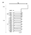
- FIG. 3 shows a band gap energy diagram of an example of the multiple quantum well light emitting layer 114 used in the nitride semiconductor light emitting device of the embodiment.
- the vertical axis in FIG. 3 indicates the thickness in the stacking direction, and the upper direction means the side closer to the p-type nitride semiconductor layer. Further, the horizontal axis of FIG. 3 indicates the magnitude of the band gap energy, and the right direction means that the band gap energy is large.
- the multiple quantum well light-emitting layer 114 includes a second light-emitting layer 142, a third barrier layer 14U, and a first light-emitting layer 141 from the side close to the p-type nitride semiconductor layer. .
- the first light emitting layer 141 includes a plurality of first quantum well layers 14W (14W1, 14W2, 14W3, 14W4, 14W5, 14W6) and a plurality of first barrier layers 14A (14A1, 14A2, 14A3, 14A4, 14A5). I have.
- the first quantum well layers 14W and the first barrier layers 14A are alternately stacked, and the first barrier layers 14A are sandwiched between the plurality of first quantum well layers 14W, respectively.
- the second light emitting layer 142 includes a plurality of second quantum well layers 14V (14V1, 14V2) and a second barrier layer 14B1 provided between the plurality of second quantum well layers 14V.
- the first barrier layer 14AZ is provided immediately above the n-type nitride semiconductor intermediate layer (superlattice layer) 122.
- the last barrier layer 14A0 is provided immediately above the second quantum well layer 14V1 located closest to the p-type nitride semiconductor layer 16 side.
- each barrier layer and each quantum well layer are generally expressed as a first barrier layer 14A, a second barrier layer 14B, a first quantum well layer 14W, and a second quantum well layer 14V, respectively.
- first barrier layer 14A a first barrier layer 14A
- second barrier layer 14B a first quantum well layer 14W
- second quantum well layer 14V a second quantum well layer 14V
- the second quantum well layer 14V has three or more layers
- the second barrier layer 14B It is also possible to have a configuration with two or more layers.
- the first barrier layer 14A is sandwiched between the plurality of first quantum well layers 14W, the first barrier layer 14A is interposed between the first barrier layer 14A and the first quantum well layer 14W.
- One or more semiconductor layers different from the one barrier layer 14A and the first quantum well layer 14W may be included.
- the length of one cycle of the first light emitting layer 141 (the sum of the thickness of the first barrier layer 14A and the thickness of the first quantum well layer 14W) can be set to, for example, 5 nm or more and 100 nm or less.
- the second barrier layer 14B is sandwiched between the plurality of second quantum well layers 14V, the second barrier layer 14B is interposed between the second barrier layer 14B and the second quantum well layer 14V.
- One or more semiconductor layers different from the second barrier layer 14B and the second quantum well layer 14V may be included.
- the thickness t 2 of the second quantum well layer 14V of the second light emitting layer 142 is made thicker than the thickness t 1 of the first quantum well layer 14W of the first light emitting layer 141. Further, it is preferable that the thickness of the second quantum well layer 14 V t 2 The difference between the thickness t 1 of the first quantum well layer 14W is 2.5nm or less. In this case, the light emission efficiency of the nitride semiconductor light emitting device during driving at a large current density can be improved.
- the second quantum well layers 14V1 and 14V2 may be formed with different thicknesses, but more preferably have the same thickness. When the thickness t 1 of the first quantum well layer 14W was extremely large difference between the thickness t 2 of the second quantum well layer 14V is undesirable shift of the emission wavelength of the nitride semiconductor light emitting device increases .
- the inventors of the present invention emitted light from the nitride semiconductor light emitting device during high temperature operation (during driving at a large current density). We found that efficiency was improved. Although the detailed principle of this action is not clear, it is presumed as follows.
- FIG. 4 is a diagram schematically illustrating the hole injection state in the second quantum well layer 14V at room temperature (25 ° C.) and at high temperature (80 ° C.). That is, when the thickness of the second quantum well layer 14V is made thicker than that of the first quantum well layer 14W, most of the holes are at the upper and lower layers of the whole quantum well layer at about room temperature (25 ° C.). In particular, when the thickness of the second quantum well layer 14V1 close to the p-type nitride semiconductor layer 16 in the second quantum well layer 14V is increased, the area of a region where many holes are present is increased. As a result, the light emission volume increases. However, even if the second quantum well layer 14V2 is similarly thickened, the expected effect cannot be obtained. This is probably because most of the holes contribute to light emission in the first quantum well layer. It is also conceivable that the crystallinity of the layer above it is deteriorated by increasing the thickness of the second layer.
- the second quantum well layer 14V1 close to the p-type nitride semiconductor layer 16 in the second quantum well layer 14V but also 2 Since holes are also injected after the second layer (second quantum well layer 14V2), the number of holes acting as carriers is less than that when only the second quantum well layer 14V1 is thick, the light output is improved, and the temperature characteristics are improved. improves.
- the thickness t 4 of the second barrier layer 14B of the second light emitting layer 142 is preferably thinner than the thickness t 3 of the third barrier layer 14U, and the thickness t 3 of the third barrier layer 14U and the second barrier layer
- the difference from the thickness t 4 of 14B is more preferably 2 nm or less.
- the thickness t 4 of the second barrier layer 14B is thinner, the light output of the nitride semiconductor light emitting element tends to increase. In particular, when considering driving at room temperature, the ratio of holes acting as carriers increases by reducing the thickness t 4 of the second barrier layer 14B.
- the thickness t 4 of the second barrier layer 14B is made extremely thin, the crystallinity of the second quantum well layer 14V stacked on the second barrier layer 14B is deteriorated, and the temperature characteristics are increased. since also tend to have lower, it is preferable to set the difference between the thickness t 4 of the thickness t 3 of the third barrier layer 14U second barrier layer 14B and 2nm or less.
- the second quantum well layer 14V is more preferably two layers.
- the thickness t 3 of the third barrier layer 14U is preferably formed to the same thickness as the thickness t 1 of the first barrier layer 14A.
- the plurality of second quantum well layers 14V1 and 14V2 preferably have a larger band gap energy than the first quantum well layer 14W ((i) in FIG. 4). Without adjusting the band gap energy between the first quantum well layer 14W and the plurality of second quantum well layers 14V1, 14V2, the second quantum well layer 14V is formed thicker than the first quantum well layer 14W as described above. In this case, since the secondary peak due to the second quantum well layer 14V appears on the short wavelength side of the emission wavelength region of the nitride semiconductor light emitting device, the half width of the emission peak of the nitride semiconductor light emitting device is large. Thus, there may be a deviation from a desired emission wavelength.
- the band gap energy of the second quantum well layer 14V larger than that of the first quantum well layer 14W and adjusting the emission wavelength of the second quantum well layer 14V to the first quantum well layer 14W, nitride semiconductor light emission
- the half width of the light emission peak of the device can be narrowed, and the emission wavelength of the nitride semiconductor light emitting device can be adjusted to a desired value.
- the second quantum well layer 14V1 closer to the p-type nitride semiconductor layer 16 is closer to the second quantum well layer 14V1 than the p-type nitride semiconductor layer 16.
- the band gap energy is preferably smaller than that of the layer 14V2 ((ii) in FIG. 4).
- the second quantum well layer 14V1 close to the p-type nitride semiconductor layer 16 can hold more holes, it can be adjusted to the actual hole distribution. The light emission efficiency of the nitride semiconductor light emitting device when driven at a density can be further improved.
- the emission wavelength of the nitride semiconductor light emitting device can be adjusted to a desired optimum value.
- the composition of the first quantum well layer 14W and the second quantum well layer 14V is changed to the nitride semiconductor. What is necessary is just to match
- the first quantum well layer 14W for example, a nitride semiconductor layer represented by the formula of Al c1 Ga d1 In (1-c1-d1) N (0 ⁇ c1 ⁇ 1, 0 ⁇ d1 ⁇ 1) is independently used. Can be used.
- the second quantum well layer 14V for example, a nitride semiconductor layer represented by an expression of Al c2 Ga d2 In (1-c2-d2) N (0 ⁇ c2 ⁇ 1, 0 ⁇ d2 ⁇ 1) is independently used. Can be used.
- the first quantum well layer 14W is In e1 Ga (1-e1) N (0 ⁇ e1 ⁇ 1) not containing Al
- the second quantum well layer 14V is In e2 Ga containing no Al.
- (1-e2) N (0 ⁇ e2 ⁇ 1, e1> e2) is preferable.
- the band gap energy of the first quantum well layer 14W and the second quantum well layer 14V can be adjusted.
- each first quantum well layer 14W and each second quantum well layer 14V are made of Al Will be included.
- each first quantum well layer 14W is larger than the In composition ratio of each second quantum well layer 14V.
- the second quantum well layer 14V1 closer to the p-type nitride semiconductor layer 16 preferably has a larger In composition ratio than the second quantum well layer 14V2 farther from the p-type nitride semiconductor layer 16. .
- the light emission efficiency of the nitride semiconductor light emitting element during driving at a large current density can be further improved.
- the second quantum well layer 14V has a two-layer structure in which the second quantum well layer 14V1 and the second quantum well layer 14V2 are arranged in this order from the side close to the p-type nitride semiconductor layer 16, the second quantum well
- the In composition ratio of the layer 14V1 is set larger than the In composition ratio of the second quantum well layer 14V2. Accordingly, since the second quantum well layer 14V1 closer to the p-type nitride semiconductor layer 16 can hold more holes, it can be adjusted to the actual distribution of holes, so that a large current is obtained.
- the light emission efficiency of the nitride semiconductor light emitting device when driven at a density can be further improved.
- a specific method for adjusting the In composition ratio several methods are conceivable. For example, a method of adjusting the temperature at the time of forming each quantum well layer is conceivable.
- the band gap energy of the second quantum well layer 14V can be made larger than that of the first quantum well layer 14W, so that the emission wavelength of the second quantum well layer 14V is set to the first quantum well layer.
- the half-value width of the emission peak of the nitride semiconductor light emitting device can be narrowed, and the emission wavelength of the nitride semiconductor light emitting device can be adjusted to a desired value.
- the second quantum well layer 14V1 closer to the p-type nitride semiconductor layer 16 has a larger In composition than the second quantum well layer 14V2, so that the second quantum well layer 14V1 closer to the p-type nitride semiconductor layer 16 is closer to the second quantum well layer 14V1.
- the two quantum well layer 14V1 has a smaller band gap energy, and the second quantum well layer 14V closer to the p-type nitride semiconductor layer 16 can hold more holes.
- the first quantum well layer 14W located on the p-type nitride semiconductor layer 16 side preferably contains as little dopant as possible. That is, it is preferable to grow the first quantum well layer 14W located on the p-type nitride semiconductor layer 16 side without introducing a dopant raw material. As a result, non-radiative recombination in each first quantum well layer 14W is less likely to occur, so that the light emission efficiency of the nitride semiconductor light emitting element when driven at a large current density can be further improved.
- the first quantum well layer 14W located on the substrate 101 side may contain an n-type dopant. As a result, the driving voltage of the nitride semiconductor light emitting device tends to decrease.
- each first quantum well layer 14W is not particularly limited, but is preferably the same.
- the quantum level of each first quantum well layer 14W is also the same, and recombination of electrons and holes in each first quantum well layer 14W.
- Light having the same wavelength is generated in each first quantum well layer 14W. This is preferable because the emission spectrum width of the nitride semiconductor light emitting device is narrowed.
- each first quantum well layer 14W when the composition and / or thickness of each first quantum well layer 14W is intentionally varied, the emission spectrum width of the nitride semiconductor light emitting device can be broadened.
- the nitride semiconductor light emitting device is used for illumination or the like, it is preferable to intentionally vary the composition and / or thickness of each first quantum well layer 14W.
- the thickness of each first quantum well layer 14W is preferably 1 nm or more and 7 nm or less. When the thickness of each first quantum well layer 14W is in the range of 1 nm or more and 7 nm or less, the light emission efficiency of the nitride semiconductor light emitting device during driving at a large current density can be further improved.
- the first barrier layer 14A (14A1 to 14A5), the second barrier layer 14B1, the third barrier layer 14U, the first barrier layer 14AZ, and the last barrier layer 14A0 respectively include the first quantum well layers 14W and the second quantum layers. It is preferable to use a nitride semiconductor material having a larger band gap energy than the nitride semiconductor material constituting the well layer 14V.
- the first barrier layer 14A (14A1 to 14A5), the second barrier layer 14B1, the third barrier layer 14U, the first barrier layer 14AZ, and the last barrier layer 14A0 are each independently Al f Ga g In (1-fg ) N (0 ⁇ f ⁇ 1,0 ⁇ it is preferable to use a nitride semiconductor layer represented by the formula g ⁇ 1), contains no Al in h Ga (1-h ) N (0 ⁇ h ⁇ 1, It is more preferable to use a nitride semiconductor layer represented by the formula e1>e2> h).
- each first barrier layer 14A is not particularly limited, but is preferably 1 nm or more and 10 nm or less, and more preferably 3 nm or more and 7 nm or less.
- the driving voltage decreases as the thickness of each first barrier layer 14A is reduced. However, if the thickness of each first barrier layer 14A is extremely reduced, the light emission efficiency of the nitride semiconductor light emitting device during driving at a large current density is achieved. Tend to decrease.
- the thickness of the first barrier layer 14AZ is not particularly limited, and is preferably 1 nm or more and 10 nm or less.
- the thickness of the last barrier layer 14A0 is not particularly limited, but is preferably 1 nm or more and 40 nm or less.
- the n-type dopant concentration in the first barrier layer 14A (14A1 to 14A5), the second barrier layer 14B1, the third barrier layer 14U, and the first barrier layer 14AZ is not particularly limited, and is preferably set as appropriate.
- the first barrier layer 14A located on the substrate 101 side is doped with an n-type dopant
- the first barrier layer 14A located on the p-type nitride semiconductor layer 16 side is doped with an n-type dopant
- the second barrier layer 14B1 and the third barrier layer 14U are preferably doped with an n-type dopant having a lower concentration than the first barrier layer 14A located on the substrate 101 side, or not doped with an n-type dopant.
- the first barrier layer 14A, the second barrier layer 14B1, the third barrier layer 14U, the first barrier layer 14AZ, and the last barrier layer 14A0 may be intentionally doped with an n-type dopant.
- the first barrier layer 14A, the second barrier layer 14B1, the third barrier layer 14U, the first barrier layer 14AZ, and the last barrier layer 14A0 include a p-type nitride semiconductor layer 16 and a p-type nitride semiconductor layer 17 respectively.
- the p-type dopant may be doped by thermal diffusion during the growth of the p-type nitride semiconductor layer 18.
- the number of first quantum well layers 14W is not particularly limited, but is preferably 2 or more and 20 or less, more preferably 3 or more and 15 or less, and more preferably 4 or more and 12 or less. Further preferred.
- a layer doped with a p-type dopant in the Al s4 Ga (1-s4) N (0 ⁇ s4 ⁇ 0.4, preferably 0.1 ⁇ s4 ⁇ 0.3) layer. More preferably, a layer doped with is used.
- the carrier concentration in the p-type nitride semiconductor layers 116, 117 and 118 is preferably 1 ⁇ 10 17 atoms / cm 3 or more. Since the activation rate of the p-type dopant is about 0.01, the p-type dopant concentration (different from the carrier concentration) in the p-type nitride semiconductor layers 116, 117, and 118 is 1 ⁇ 10 19 atoms / cm 3 or more.
- the p-type dopant concentration in the p-type nitride semiconductor layer 116 located on the multiple quantum well light-emitting layer 114 side is less than 1 ⁇ 10 19 / cm 3. It is preferable.
- the total thickness of the p-type nitride semiconductor layers 116, 117, and 118 is not particularly limited, but is preferably 50 nm or more and 300 nm or less.
- the heating time during the growth of the p-type nitride semiconductor layers 116, 117, and 118 can be shortened. Thereby, the diffusion of the p-type dopant in the p-type nitride semiconductor layers 116, 117, 118 can be suppressed.
- the n electrode 124 and the p electrode 125 are electrodes for supplying driving power to the nitride semiconductor light emitting device. As shown in FIG. 2, the n electrode 124 and the p electrode 125 are configured only by the pad electrode portion. For example, an elongated protrusion (branch electrode) for current diffusion is used as the n electrode 124 and / or the p electrode. It may be connected to the electrode 125.
- an insulating layer for preventing current from being injected into the p electrode 125 is provided below the p electrode 125. Thereby, the light emission amount shielded by the p-electrode 125 is reduced.
- the n-electrode 124 is preferably configured by, for example, a titanium layer, an aluminum layer, and a gold layer laminated in this order. Assuming that wire bonding is performed on the n-electrode 124, the thickness of the n-electrode 124 is preferably 1 ⁇ m or more.
- the p-electrode 125 is preferably composed of, for example, a nickel layer, an aluminum layer, a titanium layer, and a gold layer stacked in this order, and may be composed of the same material as the n-electrode 124. Assuming that wire bonding is performed on the p-electrode 125, the thickness of the p-electrode 125 is preferably 1 ⁇ m or more.
- the transparent electrode layer 123 is preferably made of a transparent conductive film such as ITO (Indium Tin Oxide) or IZO (Indium Zinc Oxide), and preferably has a thickness of 20 nm to 200 nm.
- ITO Indium Tin Oxide
- IZO Indium Zinc Oxide
- the carrier concentration means the concentration of electrons or holes, and is not determined only by the amount of n-type dopant or the amount of p-type dopant. Such carrier concentration is calculated based on the result of the voltage-capacitance characteristics of the nitride semiconductor light emitting device, and refers to the carrier concentration in a state where no current is injected. This is the sum of carriers generated from crystallized crystal defects and acceptor crystal defects.
- the n-type carrier concentration is almost the same as the n-type dopant concentration since the activation rate of Si or the like which is an n-type dopant is high.
- the n-type dopant concentration can be easily obtained by measuring the concentration distribution in the depth direction with SIMS (Secondary Ion Mass Spectroscopy).
- SIMS Secondary Ion Mass Spectroscopy
- the relative relationship (ratio) of the dopant concentration is almost the same as the relative relationship (ratio) of the carrier concentration. From these facts, the means for solving the problems of the present invention is defined by the dopant concentration that is actually easy to measure. And if the n-type dopant concentration obtained by the measurement is averaged in the thickness direction, the average n-type dopant concentration can be obtained.
- the buffer layer 102 is formed on the substrate 101 by sputtering, for example.
- the physical semiconductor layer 118 is formed in this order.
- the p-type nitride semiconductor layer 118, the p-type nitride semiconductor layer 117, the p-type nitride semiconductor layer 116, and the multiple quantum well light emission so that a part of the surface of the lower n-type nitride semiconductor layer 108 is exposed.
- Layer 114, n-type nitride semiconductor intermediate layer (superlattice layer) 122, n-type nitride semiconductor multilayer structure 121, low-temperature n-type nitride semiconductor layer 110, n-type nitride semiconductor modulation doped layer 109, and lower n-type nitride A part of each of the physical semiconductor layers 108 is removed by etching.
- the n-electrode 124 is formed on the surface of the lower n-type nitride semiconductor layer 108 exposed by the etching. Further, the transparent electrode layer 123 and the p electrode 125 are stacked in this order on the upper surface of the p-type nitride semiconductor layer 118.
- a transparent insulating protective film 127 is formed so as to cover the transparent electrode layer 123 and the side surface of each layer exposed by etching. Thereby, the nitride semiconductor light emitting device of the embodiment having the configuration shown in FIG. 1 is obtained.
- the structure of the nitride semiconductor light-emitting element of embodiment is not limited to the structure of the nitride semiconductor light-emitting element of the Example shown below.
- a substrate 101 which is a sapphire substrate with a diameter of 100 mm, having a concavo-convex process formed of a convex portion 101a and a concave portion 101b on its upper surface was prepared.
- the shape of the convex portion 101a is substantially circular in plan view, and the three adjacent convex portions 101a are arranged so as to be located at the apexes of a substantially equilateral triangle in plan view.
- the interval between the apexes of the adjacent convex portions 101a is 2 ⁇ m.
- the diameter of the substantially circular shape in plan view of the convex portion 101a was about 1.2 ⁇ m, and the height of the convex portion 101a was about 0.6 ⁇ m. Furthermore, the convex portion 101a and the concave portion 101b on the upper surface of the substrate 101 had the cross section shown in FIG. 1, and the convex portion 101a had a tip portion.
- RCA cleaning was performed on the upper surface of the substrate 101 after the formation of the convex portions 101a and the concave portions 101b. Then, the substrate 101 after RCA cleaning was placed in the chamber, N 2 , O 2, and Ar were introduced, and the substrate 101 was heated to 650 ° C.
- the normal direction of the surface of the substrate 101 is formed on the surface of the substrate 101 having the convex portions 101a and the concave portions 101b by a reactive sputtering method in which an Al target is sputtered in a mixed atmosphere of N 2 , O 2, and Ar.
- a buffer layer 102 having a thickness of 25 nm made of an AlON crystal made up of an aggregate of columnar crystals with uniform crystal grains extending in the same manner was formed.
- the substrate 101 on which the buffer layer 102 was formed was accommodated in the first MOCVD apparatus.
- a nitride semiconductor underlayer 107 made of undoped GaN is grown on the buffer layer 102 by MOCVD, and then the lower n-type nitride semiconductor layer 108 made of Si-doped n-type GaN is grown on the nitride semiconductor underlayer 107. Grown on the top surface.
- the thickness of the nitride semiconductor underlayer 107 is 4 ⁇ m
- the thickness of the lower n-type nitride semiconductor layer 108 is 3 ⁇ m
- the n-type dopant concentration in the lower n-type nitride semiconductor layer 108 is 1 ⁇ 10 19. / Cm 3 .
- the thickness of the nitride semiconductor underlayer 107 is preferably 1 ⁇ m or more and 8 ⁇ m or less, and more preferably 3 ⁇ m or more and 5 ⁇ m or less.
- the temperature of the substrate 101 was set to 1081 ° C. (first growth temperature), and the lower n-type nitride semiconductor layer 108 was grown on the nitride semiconductor underlayer 107.
- the lower n-type nitride semiconductor layer 108 is an n-type GaN layer having an n-type dopant concentration of 1 ⁇ 10 19 atoms / cm 3 and has a thickness of 1.5 ⁇ m.
- an n-type nitride semiconductor layer made of Si-doped n-type GaN having a thickness of 50 nm is formed on the lower n-type nitride semiconductor layer 108 with the temperature of the substrate 101 maintained at 1081 ° C. (first growth temperature).
- N-type dopant concentration 1 ⁇ 10 19 / cm 3
- 87 nm thick undoped GaN nitride semiconductor layer 50 nm thick Si doped n-type GaN n-type nitride semiconductor layer (n-type dopant)
- a nitride semiconductor layer made of undoped GaN having a concentration of 1 ⁇ 10 19 / cm 3 ) and a thickness of 87 nm was crystal-grown in this order by the MOCVD method, and an n-type nitride semiconductor modulation doped layer 109 was laminated.
- the temperature of the substrate 101 was set to 801 ° C. (second growth temperature), and the low-temperature n-type nitride semiconductor layer 110 was grown on the n-type nitride semiconductor modulation doped layer 109. Specifically, a Si-doped GaN layer having a thickness of 25 nm was grown so that the n-type dopant concentration was 1 ⁇ 10 19 atoms / cm 3 .
- the n-type nitride semiconductor multilayer structure 121 was grown on the low-temperature n-type nitride semiconductor layer 110 while maintaining the temperature of the substrate 101 at 801 ° C. (third growth temperature). Specifically, a Si-doped n-type InGaN layer having a thickness of 7 nm, a Si-doped n-type GaN layer having a thickness of 30 nm, a Si-doped n-type InGaN layer having a thickness of 7 nm, and a Si-doped n-type GaN layer having a thickness of 20 nm are formed.
- the n-type nitride semiconductor multilayer structure 121 was grown by alternately stacking two layers.
- the n-type dopant concentration in the n-type nitride semiconductor multilayer structure 121 was set to 7 ⁇ 10 17 atoms / cm 3 in any layer.
- the In composition ratio of the InGaN layer was set to be the same as the In composition ratio of the narrow band gap layer constituting the n-type nitride semiconductor intermediate layer (superlattice layer) 122 to be grown next.
- an n-type nitride semiconductor intermediate layer (superlattice layer) 122 is grown on the n-type nitride semiconductor multilayer structure 121 with the temperature of the substrate 101 maintained at 801 ° C. (fourth growth temperature). It was. Specifically, a wide band gap layer made of a Si-doped n-type GaN layer and a narrow band gap layer made of a Si-doped n-type InGaN layer are alternately grown on the n-type nitride semiconductor multilayer structure 121 for 20 periods. It was. The thickness of each wide band gap layer was 2.05 nm. Moreover, the thickness of each narrow band gap layer was 2.05 nm.
- the n-type dopant concentration in each wide band gap layer is 1 ⁇ 10 19 / cm 3 for five wide band gap layers located on the multiple quantum well light emitting layer 114 side, and is located on the substrate 101 side from that.
- the number of wide band gap layers was 0 / cm 3 (undoped).
- first barrier layers 14A 14A1 to 14A5 made of InGaN and first quantum well layers 14W (14W1 to 14W6) made of InGaN are alternately grown one by one.
- the third barrier layer 14U made of InGaN is grown, and the temperature of the substrate 101 is further raised to 678 ° C., and then the second quantum well layer 14V1 made of InGaN and the second barrier layer 14B1 made of InGaN are alternately layered one by one.
- the second quantum well layer 14V2 made of InGaN was grown.
- the thickness of each first barrier layer 14A, third barrier layer 14U, and second barrier layer 14B was 4.52 nm.
- the n-type dopant concentration in the first barrier layer 14AZ and the first barrier layers 14A5 and 14A4 is 4.3 ⁇ 10 18 atoms / cm 3 , and the other first barrier layer 14A3, first barrier 14A2, first barrier 14A1, The third barrier layer 14U and the second barrier layer 14B were undoped.
- the thickness t 4 of the second barrier layer 14B1 is preferably 0 ⁇ t 4 ⁇ 4.52 nm, and more preferably 3 nm ⁇ t 4 ⁇ 4.52 nm.
- the thickness t 4 of the second barrier layer 14B1 is less than 3 nm, the function as a crystal recovery layer becomes insufficient, and the crystallinity of the second quantum well layer 14V1 to be stacked next decreases, so that the There is a possibility that a desired light output (Po) cannot be obtained during driving.
- the first barrier layer 14A1 is doped with an n-type dopant by 4 ⁇ 10 17 atoms / cm 3 or more and 4 ⁇ 10 18 atoms / cm 3 or less, deterioration of the temperature characteristics of the nitride semiconductor light emitting device can be suppressed. Therefore, it is possible to improve the light output (Po) of the nitride semiconductor light emitting device during driving at a large current density.
- the first barrier layer 14AZ is formed for the purpose of forming a narrow band gap layer located closest to the multiple quantum well light-emitting layer 114 in the n-type nitride semiconductor intermediate layer (superlattice layer) 122, and for the n-type nitride semiconductor intermediate layer (AZ).
- the thickness may be larger than the thickness of the first barrier layer 14A5 (for example, thick). 5.52 nm).
- the n-type dopant concentration in the first barrier layer 14AZ is 1 ⁇ 10 19 / cm 3 in the lower part of the first barrier layer 14AZ (a region separated by 2.05 nm or more from the lower surface of the first barrier layer 14AZ),
- the upper portion of the first barrier layer 14Az (a portion other than the lower portion of the first barrier layer 14Az) may be 4.3 ⁇ 10 18 pieces / cm 3 .
- the n-type dopant is doped only in the lower part of the first barrier layer 14A4 (for example, a region 3.5 nm away from the lower surface of the first barrier layer 14A4), and the upper part of the first barrier layer 14A4 (lower part of the first barrier layer 14A4). Other parts) may be undoped.
- the upper part of the first barrier layer 14A4 undoped it is possible to prevent the injected carriers of the first quantum well layer 14W4 from coming into direct contact with the n-type doped barrier layer portion.
- the thickness of each first quantum well layer 14W was 3.38 nm.
- the In composition x in the first quantum well layer 14W was set by adjusting the TMI flow rate so that the wavelength of light emitted from the first quantum well layer 14W by photoluminescence was 448 nm.
- the thickness of each second quantum well layer 14V was 4.24 nm. It has been found that the light output (Po) in a room temperature (25 ° C.) environment is improved by making the thickness of the second quantum well layer 14V thicker than that of the first quantum well layer 14W.
- the thickness of the second quantum well layer 14V is set to a very large thickness of about 10 to 15 nm, an effect of improving the optical output (Po) should be obtained.
- the thickness of the film was 5.6 nm or more, the effect of improving the light output (Po) in a room temperature (25 ° C.) environment could not be obtained.
- the thicknesses of the second quantum well layer 14V1 and the second quantum well layer 14V2 were each set to 4.0 nm. In this case, it has been found that the light output (Po) in a high temperature (80 ° C.) environment (during driving at a large current density) is further improved.
- the In composition ratio in the first quantum well layer 14W was set by adjusting the flow rate of TMI so that the wavelength of light emitted from the first quantum well layer 14W by photoluminescence was 448 nm.
- the In composition ratio of each of the second quantum well layers 14V1 and V2 was adjusted to the optimum value by adjusting the temperature of the substrate 101 as described above.
- the last barrier layer 14A0 (thickness 10 nm) made of an undoped GaN layer was grown on the uppermost first quantum well layer 14W1.
- the temperature of the substrate 101 is raised to 1000 ° C., and a p-type Al 0.18 Ga 0.82 N layer and a p-type are formed on the top surface of the last barrier layer 14A0 as p-type nitride semiconductor layers 116, 117, and 118, respectively.
- a GaN layer and a p-type contact layer were grown.
- TMG trimethylgallium
- TMA trimethylaluminum
- TMI trimethylindium
- NH 3 was used as the N source gas
- SiH 4 was used as a source gas for Si as an n-type dopant
- Cp 2 Mg was used as a source gas for Mg as a p-type dopant.
- the source gas is not limited to the above gas, and any gas that can be used as a MOCVD source gas can be used without limitation.
- TEG triethylgallium
- TEA triethylaluminum
- Al aluminum
- TEI triethylindium
- An organic nitrogen compound such as DMHy (dimethylhydrazine) can be used as the N source gas
- Si 2 H 6 or organic Si can be used as the Si source gas.
- a p-type contact layer (p-type nitride semiconductor layer 118), a p-type GaN layer (p-type nitride semiconductor layer 117), p so that a part of the surface of the lower n-type nitride semiconductor layer 108 is exposed.
- Type AlGaN layer (p-type nitride semiconductor layer 116), multiple quantum well light emitting layer 114, n-type nitride semiconductor intermediate layer (superlattice layer) 122, n-type nitride semiconductor multilayer structure 121, low-temperature n-type nitride semiconductor
- Each part of layer 110 and n-type nitride semiconductor modulation doped layer 109 was etched.
- n electrode 124 made of Au was formed on the upper surface of the lower n-type nitride semiconductor layer 108 exposed by this etching. Further, a transparent electrode layer 123 made of ITO and a p electrode 125 made of Au were sequentially formed on the upper surface of the p-type contact layer 118. Further, a transparent insulating protective film 127 made of SiO 2 was formed so as to mainly cover the transparent electrode layer 123 and the side surfaces of each layer exposed by the etching.
- the substrate 101 was divided into 620 ⁇ 680 ⁇ m size chips. Thereby, the nitride semiconductor light emitting device of the example was obtained.
- each first quantum well layer 14W being 3.38 nm and the thickness of each second quantum well layer 14V1 being 3.38 nm, the same as in the nitride semiconductor light emitting device of the example, A nitride semiconductor light emitting device of a comparative example was produced.
- the present invention includes an n-type nitride semiconductor layer, a p-type nitride semiconductor layer, and a multiple quantum well light-emitting layer provided between the n-type nitride semiconductor layer and the p-type nitride semiconductor layer.
- the quantum well light-emitting layer includes a second light-emitting layer, a third barrier layer, and a first light-emitting layer from the side close to the p-type nitride semiconductor layer, and the first light-emitting layer includes a plurality of first quantum well layers and And a first barrier layer provided between the plurality of first quantum well layers, and the second light emitting layer is provided between the plurality of second quantum well layers and the plurality of second quantum well layers.
- a nitride semiconductor light emitting device having a second barrier layer, wherein the second quantum well layer is thicker than the first quantum well layer By adopting such a configuration, it is possible to provide a nitride semiconductor light emitting device capable of improving the light emission efficiency during driving at a large current density.
- the number of second quantum well layers is preferably two. In this case, the light emission efficiency during driving at a large current density can be further improved.
- the second barrier layer is preferably thinner than at least one of the first barrier layer and the third barrier layer. Furthermore, it is more preferable that the third barrier layer has the same thickness as the first barrier layer. With such a configuration, the light output of the nitride semiconductor light emitting device can be increased.
- the second quantum well layer has a larger band gap energy than the first quantum well layer.
- the band gap energy is smaller in the plurality of second quantum well layers closer to the p-type nitride semiconductor layer.
- the first quantum well layer is made of Al c1 Ga d1 In (1-c1-d1) N (0 ⁇ c1 ⁇ 1, 0 ⁇ d1 ⁇ 1).
- the two quantum well layers are made of Al c2 Ga d2 In (1-c2-d2) N (0 ⁇ c2 ⁇ 1, 0 ⁇ d2 ⁇ 1), and the In composition ratio of the first quantum well layer is the second quantum well layer. It is preferable that it is larger than the In composition ratio.
- the plurality of second quantum well layers have a larger In composition ratio closer to the p-type nitride semiconductor layer.
- the present invention can be used for a nitride semiconductor light emitting device.
Landscapes
- Led Devices (AREA)
- Semiconductor Lasers (AREA)
Abstract
Description
図1に、本発明の窒化物半導体発光素子の一例である実施の形態の窒化物半導体発光素子の模式的な断面図を示す。図2に、図1に示す実施の形態の窒化物半導体発光素子を上面から見た模式的な平面図を示す。
基板101としては、たとえば、サファイアなどの絶縁性基板、またはGaN、SiC若しくはZnOなどの導電性基板を用いることができる。基板101の厚さは特に限定されないが、窒化物半導体層の成長時における基板101の厚さは、900μm以上1200μmであることが好ましく、窒化物半導体発光素子の使用時の基板101の厚さは、50μm以上300μm以下であることが好ましい。
バッファ層102としては、たとえばAls0Gat0Ou0N1-u0(0≦s0≦1、0≦t0≦1、0≦u0≦1、s0+t0≠0)からなる式で表わされる窒化物半導体層を用いることが好ましく、AlN層またはAlON層であることがより好ましい。
窒化物半導体下地層107は、たとえば、MOCVD(Metal Organic Chemical Vapor Deposition)法により、バッファ層102の表面上に形成することができる。
下部n型窒化物半導体層108としては、たとえば、Alx1Gay1Inz1N(0≦x1≦1、0≦y1≦1、0≦z1≦1、x1+y1+z1≠0)の式で表わされるIII族窒化物半導体からなる層にn型ドーパントがドープされた層を用いることができる。なかでも、下部n型窒化物半導体層108としては、Alx2Ga1-x2N(0≦x2≦1、好ましくは0≦x2≦0.5、より好ましくは0≦x2≦0.1)層にn型ドーパントがドープされた層を用いることがより好ましい。
下部n型窒化物半導体層108以外のn型窒化物半導体層(n型窒化物半導体変調ドープ層109、低温n型窒化物半導体層110、n型窒化物半導体多層構造体121、n型窒化物半導体中間層(超格子層)122)は、単層であってもよく、組成および/またはドーパント濃度の異なる複数層であってもよい。
図3に、実施の形態の窒化物半導体発光素子に用いられる多重量子井戸発光層114の一例のバンドギャップエネルギー図を示す。図3の縦軸は積層方向の厚さを示しており、上方向がp型窒化物半導体層に近い側を意味している。また、図3の横軸はバンドギャップエネルギーの大きさを示しており、右方向がバンドギャップエネルギーが大きいことを意味している。
p型窒化物半導体層116,117,118としては、それぞれ独立に、たとえばAls4Gat4Inu4N(0≦s4≦1、0≦t4≦1、0≦u4≦1、s4+t4+u4≠0)層にp型ドーパントがドープされた層を用いることが好ましく、Als4Ga(1-s4)N(0<s4≦0.4、好ましくは0.1≦s4≦0.3)層にp型ドーパントがドープされた層を用いることがより好ましい。
n電極124およびp電極125は、窒化物半導体発光素子に駆動電力を供給するための電極である。図2に示すように、n電極124およびp電極125は、パッド電極部分のみで構成されているが、たとえば電流拡散を目的とする細長い突出部(枝電極)などがn電極124および/またはp電極125に接続されていてもよい。
キャリア濃度は電子またはホールの濃度を意味し、n型ドーパントの量またはp型ドーパントの量だけでは決定されない。このようなキャリア濃度は窒化物半導体発光素子の電圧対容量特性の結果に基づいて算出されるものであり、電流が注入されていない状態のキャリア濃度のことを指しており、イオン化した不純物、ドナー化した結晶欠陥およびアクセプター化した結晶欠陥から発生したキャリアの合計である。
以下に、実施の形態の窒化物半導体発光素子の製造方法の一例について説明する。まず、たとえばスパッタ法などにより、基板101の上にバッファ層102を形成する。
まず、図1に示すように、凸部101aおよび凹部101bからなる凹凸加工が上面に施された100mm径のサファイア基板である基板101を準備した。凸部101aの形状は、平面視において略円形を為し、隣り合う3個の凸部101aが平面視において略正三角形の頂点に位置するように配置されている。隣り合う凸部101aの頂点の間隔は2μmである。
Claims (5)
- n型窒化物半導体層と、
p型窒化物半導体層と、
前記n型窒化物半導体層と前記p型窒化物半導体層との間に設けられた多重量子井戸発光層と、を備え、
前記多重量子井戸発光層は、前記p型窒化物半導体層に近い側から、第2発光層と、第3バリア層と、第1発光層とを備え、
前記第1発光層は、複数の第1量子井戸層と、前記複数の第1量子井戸層の間に設けられた第1バリア層とを備え、
前記第2発光層は、複数の第2量子井戸層と、前記複数の第2量子井戸層の間に設けられた第2バリア層とを備え、
前記第2量子井戸層は、前記第1量子井戸層よりも厚い、窒化物半導体発光素子。 - 前記第2バリア層は、前記第1バリア層よりも薄い、請求項1に記載の窒化物半導体発光素子。
- 前記第2量子井戸層は、前記第1量子井戸層よりもバンドギャップエネルギーが大きい、請求項1または2に記載の窒化物半導体発光素子。
- 前記複数の第2量子井戸層において、前記p型窒化物半導体層に近い方がバンドギャップエネルギーが小さい、請求項3に記載の窒化物半導体発光素子。
- 前記第1量子井戸層は、Alc1Gad1In(1-c1-d1)N(0≦c1<1、0<d1≦1)からなり、
前記第2量子井戸層は、Alc2Gad2In(1-c2-d2)N(0≦c2<1、0<d2≦1)からなり、
前記第1量子井戸層のIn組成比は、前記第2量子井戸層のIn組成比よりも大きい、請求項1から4のいずれか1項に記載の窒化物半導体発光素子。
Priority Applications (3)
| Application Number | Priority Date | Filing Date | Title |
|---|---|---|---|
| US14/394,059 US9318645B2 (en) | 2012-10-19 | 2013-10-16 | Nitride semiconductor light-emitting element |
| CN201380023054.3A CN104272477B (zh) | 2012-10-19 | 2013-10-16 | 氮化物半导体发光元件 |
| JP2014542156A JPWO2014061692A1 (ja) | 2012-10-19 | 2013-10-16 | 窒化物半導体発光素子 |
Applications Claiming Priority (2)
| Application Number | Priority Date | Filing Date | Title |
|---|---|---|---|
| JP2012232074 | 2012-10-19 | ||
| JP2012-232074 | 2012-10-19 |
Publications (1)
| Publication Number | Publication Date |
|---|---|
| WO2014061692A1 true WO2014061692A1 (ja) | 2014-04-24 |
Family
ID=50488253
Family Applications (1)
| Application Number | Title | Priority Date | Filing Date |
|---|---|---|---|
| PCT/JP2013/078042 Ceased WO2014061692A1 (ja) | 2012-10-19 | 2013-10-16 | 窒化物半導体発光素子 |
Country Status (4)
| Country | Link |
|---|---|
| US (1) | US9318645B2 (ja) |
| JP (1) | JPWO2014061692A1 (ja) |
| CN (1) | CN104272477B (ja) |
| WO (1) | WO2014061692A1 (ja) |
Cited By (3)
| Publication number | Priority date | Publication date | Assignee | Title |
|---|---|---|---|---|
| CN107210339A (zh) * | 2015-02-05 | 2017-09-26 | 同和电子科技有限公司 | 第iii族氮化物半导体发光元件和其制造方法 |
| JP2022101442A (ja) * | 2020-12-24 | 2022-07-06 | 日亜化学工業株式会社 | 窒化物半導体発光素子およびその製造方法 |
| US12527122B2 (en) | 2020-12-23 | 2026-01-13 | Nichia Corporation | Nitride semiconductor light emitting element |
Families Citing this family (16)
| Publication number | Priority date | Publication date | Assignee | Title |
|---|---|---|---|---|
| CN106410005B (zh) * | 2016-10-18 | 2018-09-04 | 华灿光电(浙江)有限公司 | 一种氮化镓基led外延片及其生长方法 |
| CN106887493B (zh) * | 2017-02-15 | 2019-08-23 | 华灿光电(浙江)有限公司 | 一种发光二极管的外延片及其制备方法 |
| JP6379265B1 (ja) * | 2017-09-12 | 2018-08-22 | 日機装株式会社 | 窒化物半導体発光素子及び窒化物半導体発光素子の製造方法 |
| US11302248B2 (en) | 2019-01-29 | 2022-04-12 | Osram Opto Semiconductors Gmbh | U-led, u-led device, display and method for the same |
| CN121583214A (zh) | 2019-01-29 | 2026-02-27 | 奥斯兰姆奥普托半导体股份有限两合公司 | 视频墙、驱动器电路、控制系统及其方法 |
| CN121815845A (zh) * | 2019-01-29 | 2026-04-07 | 奥斯兰姆奥普托半导体股份有限两合公司 | 微型发光二极管、微型发光二极管装置、显示器及其方法 |
| US11271143B2 (en) | 2019-01-29 | 2022-03-08 | Osram Opto Semiconductors Gmbh | μ-LED, μ-LED device, display and method for the same |
| WO2020229576A2 (de) | 2019-05-14 | 2020-11-19 | Osram Opto Semiconductors Gmbh | Beleuchtungseinheit, verfahren zur herstellung einer beleuchtungseinheit, konverterelement für ein opto-elektronisches bauelement, strahlungsquelle mit einer led und einem konverterelement, auskoppelstruktur, und optoelektronische vorrichtung |
| KR20210120106A (ko) | 2019-02-11 | 2021-10-06 | 오스람 옵토 세미컨덕터스 게엠베하 | 광전자 부품, 광전자 조립체 및 방법 |
| JP7604394B2 (ja) | 2019-04-23 | 2024-12-23 | エイエムエス-オスラム インターナショナル ゲーエムベーハー | Ledモジュール、ledディスプレイモジュール、および当該モジュールを製造する方法 |
| US11538852B2 (en) | 2019-04-23 | 2022-12-27 | Osram Opto Semiconductors Gmbh | μ-LED, μ-LED device, display and method for the same |
| KR102947058B1 (ko) | 2019-05-13 | 2026-04-01 | 에이엠에스-오스람 인터내셔널 게엠베하 | 다중 칩 캐리어 구조체 |
| WO2020233873A1 (de) | 2019-05-23 | 2020-11-26 | Osram Opto Semiconductors Gmbh | Beleuchtungsanordnung, lichtführungsanordnung und verfahren |
| CN114730824A (zh) | 2019-09-20 | 2022-07-08 | 奥斯兰姆奥普托半导体股份有限两合公司 | 光电组件、半导体结构和方法 |
| JP7469677B2 (ja) * | 2019-11-26 | 2024-04-17 | 日亜化学工業株式会社 | 窒化物半導体素子 |
| CN113675304A (zh) * | 2021-08-20 | 2021-11-19 | 江西兆驰半导体有限公司 | 一种氮化镓基发光二极管及其制作方法 |
Citations (3)
| Publication number | Priority date | Publication date | Assignee | Title |
|---|---|---|---|---|
| JP2004179428A (ja) * | 2002-11-27 | 2004-06-24 | Rohm Co Ltd | 半導体発光素子 |
| JP2007115753A (ja) * | 2005-10-18 | 2007-05-10 | Sumitomo Electric Ind Ltd | 窒化物半導体発光素子 |
| JP2011187621A (ja) * | 2010-03-08 | 2011-09-22 | Nichia Corp | 窒化物系半導体発光素子 |
Family Cites Families (7)
| Publication number | Priority date | Publication date | Assignee | Title |
|---|---|---|---|---|
| JP2006108585A (ja) * | 2004-10-08 | 2006-04-20 | Toyoda Gosei Co Ltd | Iii族窒化物系化合物半導体発光素子 |
| JP2007281257A (ja) | 2006-04-07 | 2007-10-25 | Toyoda Gosei Co Ltd | Iii族窒化物半導体発光素子 |
| KR20080035865A (ko) | 2006-10-20 | 2008-04-24 | 삼성전자주식회사 | 반도체 발광 소자 |
| DE102007058723A1 (de) * | 2007-09-10 | 2009-03-12 | Osram Opto Semiconductors Gmbh | Lichtemittierende Struktur |
| KR100993085B1 (ko) * | 2009-12-07 | 2010-11-08 | 엘지이노텍 주식회사 | 발광 소자, 발광 소자 패키지 및 라이트 유닛 |
| US8525148B2 (en) * | 2010-07-16 | 2013-09-03 | Micron Technology, Inc. | Solid state lighting devices without converter materials and associated methods of manufacturing |
| JP5044704B2 (ja) | 2010-08-26 | 2012-10-10 | 株式会社東芝 | 半導体発光素子 |
-
2013
- 2013-10-16 WO PCT/JP2013/078042 patent/WO2014061692A1/ja not_active Ceased
- 2013-10-16 CN CN201380023054.3A patent/CN104272477B/zh active Active
- 2013-10-16 JP JP2014542156A patent/JPWO2014061692A1/ja active Pending
- 2013-10-16 US US14/394,059 patent/US9318645B2/en not_active Expired - Fee Related
Patent Citations (3)
| Publication number | Priority date | Publication date | Assignee | Title |
|---|---|---|---|---|
| JP2004179428A (ja) * | 2002-11-27 | 2004-06-24 | Rohm Co Ltd | 半導体発光素子 |
| JP2007115753A (ja) * | 2005-10-18 | 2007-05-10 | Sumitomo Electric Ind Ltd | 窒化物半導体発光素子 |
| JP2011187621A (ja) * | 2010-03-08 | 2011-09-22 | Nichia Corp | 窒化物系半導体発光素子 |
Cited By (4)
| Publication number | Priority date | Publication date | Assignee | Title |
|---|---|---|---|---|
| CN107210339A (zh) * | 2015-02-05 | 2017-09-26 | 同和电子科技有限公司 | 第iii族氮化物半导体发光元件和其制造方法 |
| US12527122B2 (en) | 2020-12-23 | 2026-01-13 | Nichia Corporation | Nitride semiconductor light emitting element |
| JP2022101442A (ja) * | 2020-12-24 | 2022-07-06 | 日亜化学工業株式会社 | 窒化物半導体発光素子およびその製造方法 |
| JP7260807B2 (ja) | 2020-12-24 | 2023-04-19 | 日亜化学工業株式会社 | 窒化物半導体発光素子およびその製造方法 |
Also Published As
| Publication number | Publication date |
|---|---|
| CN104272477A (zh) | 2015-01-07 |
| JPWO2014061692A1 (ja) | 2016-09-05 |
| CN104272477B (zh) | 2017-11-10 |
| US20150076447A1 (en) | 2015-03-19 |
| US9318645B2 (en) | 2016-04-19 |
Similar Documents
| Publication | Publication Date | Title |
|---|---|---|
| US9318645B2 (en) | Nitride semiconductor light-emitting element | |
| US9620671B2 (en) | Nitride semiconductor light emitting element and method for manufacturing same | |
| US8575592B2 (en) | Group III nitride based light emitting diode structures with multiple quantum well structures having varying well thicknesses | |
| CN104919604B (zh) | 氮化物半导体发光元件 | |
| TWI466330B (zh) | 三族氮化物半導體發光元件 | |
| JP6306200B2 (ja) | 窒化物半導体発光素子 | |
| US9373750B2 (en) | Group III nitride semiconductor light-emitting device | |
| US8835902B2 (en) | Nano-structured light-emitting devices | |
| JP6026116B2 (ja) | 窒化物半導体発光素子およびその製造方法 | |
| JPWO2008153130A1 (ja) | 窒化物半導体発光素子及び窒化物半導体の製造方法 | |
| KR100752007B1 (ko) | 3족 질화물계 화합물 반도체 발광 소자 및 그 제조 방법 | |
| JP2011171369A (ja) | 半導体発光素子 | |
| US20170186912A1 (en) | Nitride semiconductor light-emitting element | |
| JP2009224370A (ja) | 窒化物半導体デバイス | |
| JP2012248763A5 (ja) | ||
| KR101025971B1 (ko) | 질화물 반도체 발광소자 | |
| JP6486401B2 (ja) | 半導体発光素子および半導体発光素子の製造方法 | |
| JP2012515445A (ja) | オプトエレクトロニクス半導体部品 | |
| TWI545798B (zh) | Nitride semiconductor light emitting device and manufacturing method thereof | |
| JP6482388B2 (ja) | 窒化物半導体発光素子 | |
| JP5337862B2 (ja) | 半導体発光素子 | |
| JP2008227103A (ja) | GaN系半導体発光素子 | |
| US9508895B2 (en) | Group III nitride semiconductor light-emitting device and production method therefor |
Legal Events
| Date | Code | Title | Description |
|---|---|---|---|
| ENP | Entry into the national phase |
Ref document number: 2014542156 Country of ref document: JP Kind code of ref document: A |
|
| 121 | Ep: the epo has been informed by wipo that ep was designated in this application |
Ref document number: 13847724 Country of ref document: EP Kind code of ref document: A1 |
|
| WWE | Wipo information: entry into national phase |
Ref document number: 14394059 Country of ref document: US |
|
| NENP | Non-entry into the national phase |
Ref country code: DE |
|
| 122 | Ep: pct application non-entry in european phase |
Ref document number: 13847724 Country of ref document: EP Kind code of ref document: A1 |