WO2014061115A1 - Led照明調光回路、および、led照明調光方法 - Google Patents
Led照明調光回路、および、led照明調光方法 Download PDFInfo
- Publication number
- WO2014061115A1 WO2014061115A1 PCT/JP2012/076783 JP2012076783W WO2014061115A1 WO 2014061115 A1 WO2014061115 A1 WO 2014061115A1 JP 2012076783 W JP2012076783 W JP 2012076783W WO 2014061115 A1 WO2014061115 A1 WO 2014061115A1
- Authority
- WO
- WIPO (PCT)
- Prior art keywords
- dimming
- period
- mode
- dimming rate
- control circuit
- Prior art date
- Legal status (The legal status is an assumption and is not a legal conclusion. Google has not performed a legal analysis and makes no representation as to the accuracy of the status listed.)
- Ceased
Links
Images



Classifications
-
- H—ELECTRICITY
- H05—ELECTRIC TECHNIQUES NOT OTHERWISE PROVIDED FOR
- H05B—ELECTRIC HEATING; ELECTRIC LIGHT SOURCES NOT OTHERWISE PROVIDED FOR; CIRCUIT ARRANGEMENTS FOR ELECTRIC LIGHT SOURCES, IN GENERAL
- H05B45/00—Circuit arrangements for operating light-emitting diodes [LED]
- H05B45/10—Controlling the intensity of the light
Definitions
- the present invention relates to an LED illumination dimming circuit and an LED illumination dimming method.
- LED illumination dimming circuit 100A that controls dimming of an LED element as described in, for example, Japanese Patent Application Laid-Open Nos. 2009-123682 and 2012-59662 (FIG. 4).
- This LED illumination dimming circuit 100A is connected between a resistor R1, a bipolar transistor Q1 whose collector is connected to the cathode of the LED element 4 whose anode is connected to the power source 2, and an emitter of the bipolar transistor Q1 and the ground.
- the constant current circuit 6 and the microcomputer 5 that controls the bipolar transistor Q1 and the constant current circuit 6 according to the dimming signal output from the dimmer 1 are provided (FIG. 4).
- the bipolar transistor Q1 is controlled to perform dimming (linear dimming) by reducing the peak current.
- An LED illumination dimming circuit includes: An LED illumination dimming circuit for controlling dimming of the LED element, A power supply terminal to which a power supply voltage is supplied; A ground terminal connected to ground, and A first output terminal connected to the power supply terminal and connected to the anode side of the LED element; A second output terminal to which the cathode side of the LED element is connected; A capacitor having one end connected to the first output terminal and the other end connected to the second output terminal; A coil having one end connected to the other end of the capacitor; A switching element having one end connected to the other end of the coil; A resistor having one end connected to the other end of the switch element and the other end connected to the ground terminal; A diode having a cathode connected to the power supply terminal and an anode connected to the other end of the coil; A control circuit for controlling the operation of the switch element by a switch control signal in response to a dimming signal indicating a dimming rate of the LED element, The control circuit includes: In the
- the dimming signal indicates a dimming rate of a first dimming section from the first dimming rate to a second dimming rate lower than the first dimming rate
- the switching cycle is reduced while maintaining the ratio of the on period and the off period
- the dimming signal indicates a dimming rate of a second dimming section from the second dimming rate to a third dimming rate lower than the second dimming rate
- the dimming rate indicated by the dimming signal decreases, the on period is shortened while the off period is fixed.
- the control circuit includes: In the second mode, when the dimming rate indicated by the dimming signal increases, the switching period is increased while maintaining the ratio between the on period and the off period.
- the control circuit includes: In the third mode, when the dimming rate indicated by the dimming signal increases, the on period is lengthened while the off period is fixed.
- the control circuit includes: In a fourth mode in which the dimming signal indicates a dimming rate of a third dimming section from the third dimming rate to a fourth dimming rate lower than the third dimming rate.
- the dimming rate indicated by the dimming signal decreases, the off period is lengthened while the on period is shortened.
- the control circuit includes: In the fourth mode, when the dimming rate indicated by the dimming signal increases, the off period is shortened while the on period is lengthened.
- the control circuit includes: In the fifth mode in which the dimming signal indicates the dimming rate of the fourth dimming rate, the on period is fixed, and the off period is fixed to a period longer than the off period in the fourth mode. It is characterized by.
- the control circuit When the control circuit shifts from the first mode to the second mode, the control circuit reduces the switching period while maintaining the ratio between the on period and the off period, and then starts the second mode from the second mode.
- the on period When shifting to the third mode, the on period is shortened while the off period is fixed.
- the control circuit includes: When shifting from the second mode to the first mode, the switching period is increased while maintaining the ratio between the on period and the off period.
- the control circuit includes: When shifting from the third mode to the second mode, the on period is lengthened while the off period is fixed.
- the control circuit includes: When shifting from the third mode to the fourth mode, the off period is lengthened while the on period is shortened.
- the control circuit shifts from the fourth mode to the third mode, the control circuit shortens the off period while extending the on period.
- the control circuit includes: When shifting from the fourth mode to the fifth mode, the off period is set longer than the off period in the fourth mode while maintaining the on period. When shifting from the fifth mode to the fourth mode, the off period is shorter than the off period in the fifth mode while maintaining the on period.
- the switching frequency that is the reciprocal of the switching period corresponding to the first dimming rate in the first mode is higher than the audible frequency.
- An LED illumination dimming circuit for controlling dimming of an LED element, wherein a power supply terminal to which a power supply voltage is supplied, a ground terminal connected to ground, the anode terminal of the LED element is connected to the power supply terminal One end connected to the first output terminal connected, the second output terminal connected to the cathode side of the LED element, and the first output terminal, and the other end connected to the second output terminal.
- a capacitor having one end connected to the other end of the capacitor, a switch element having one end connected to the other end of the coil, one end connected to the other end of the switch element, and the other to the ground terminal
- a switch control signal in accordance with a resistor having an end connected thereto, a diode having a cathode connected to the power supply terminal and an anode connected to the other end of the coil, and a dimming signal indicating a dimming rate of the LED element
- Ri A LED lighting dimming method according to the LED lighting dimmer circuit and a control circuit for controlling the operation of said switching element, In the first mode in which the dimming signal exhibits a first dimming rate, a switching period consisting of an on period in which the switch element is turned on and an off period in which the switch element is turned off is fixed.
- the dimming signal indicates a dimming rate of a first dimming section from the first dimming rate to a second dimming rate lower than the first dimming rate
- the switching cycle is reduced while maintaining the ratio of the on period and the off period
- the dimming signal indicates a dimming rate of a second dimming section from the second dimming rate to a third dimming rate lower than the second dimming rate
- the dimming rate indicated by the dimming signal decreases, the on period is shortened while the off period is fixed.
- the OFF width of the switch element is modulated so that the switching frequency does not become too high at the time of dimming, and the maximum dimming range is made possible within a limited frequency range.
- Dimming is performed in five modes. That is, the maximum current mode in which the LED element emits light at the maximum current, the frequency modulation mode in which dimming is performed by reducing the peak current, the off width fixed mode in which only the on width is narrowed by fixing the off width, and the off width is extended.
- the five modes of the off width modulation mode for narrowing the on width and the minimum current mode for causing the LED element to emit light with the minimum current are continuously executed.
- the frequency fluctuation range can be narrowed by increasing the OFF width of the switch element while reducing the ON width of the switch element.
- the control is to lower the switching frequency when the dimming rate is low (when it is dark), the current (energy) is minimum when it approaches the audible frequency.
- the LED illumination dimming circuit according to the present invention can realize a wide dimming range in a narrow frequency fluctuation range.
- the frequency fluctuation can be reduced while taking advantage of the current critical mode with high efficiency and low noise.
- FIG. 1 is a diagram illustrating an example of a configuration of an LED illumination dimming circuit 100 according to a first embodiment which is an aspect of the present invention.
- FIG. 2 is a diagram illustrating an example of operation waveforms in each mode of the LED illumination dimming circuit 100 illustrated in FIG. 1.
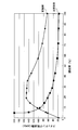
- FIG. 3 is a characteristic diagram showing the relationship between the dimming rate and the switching frequency of the LED illumination dimming circuit 100 shown in FIG. 1 and the conventional LED illumination dimming circuit.
- FIG. 4 is a diagram illustrating an example of a configuration of a conventional LED illumination dimming circuit 100A.
- FIG. 1 is a diagram illustrating an example of a configuration of an LED illumination dimming circuit 100 according to a first embodiment which is an aspect of the present invention.
- FIG. 2 is a figure which shows an example of the operation waveform in each mode of the LED illumination light control circuit 100 shown in FIG.
- the LED illumination dimming circuit 100 includes a power supply terminal TB, a ground terminal TE, a first output terminal TOUT1, a second output terminal TOUT2, a capacitor C, a coil L, and a resistor. R, a switch element SW, and a control circuit CON are provided.
- a power supply voltage is supplied to the power supply terminal TB.
- a positive electrode of a battery (power source) B is connected to the power source terminal TB.
- the ground terminal TE is connected to the ground.
- the negative terminal of the battery (power source) B is connected to the ground terminal TE.
- the first output terminal TOUT1 is connected to the power supply terminal TB, and the anode side of the LED element A is connected thereto.
- the second output terminal TOUT2 is connected to the cathode side of the LED element A.
- the capacitor C has one end connected to the first output terminal TOUT1 and the other end connected to the second output terminal TOUT2.
- the coil L has one end connected to the other end of the capacitor C.
- the switch element SW has one end connected to the other end of the coil L.
- the resistor R has one end connected to the other end of the switch element SW and the other end connected to the ground terminal TE.
- the diode D has a cathode connected to the power supply terminal TB and an anode connected to the other end of the coil L.
- the control circuit CON controls the operation of the switch element SW by the switch control signal GATE according to the dimming signal REF indicating the dimming rate of the LED element A.
- the switch element SW has one end connected to the other end of the coil L, the other end connected to one end of the resistor R, and a MOS transistor (in the example of FIG. 1) to which the switch control signal GATE is supplied to the gate. , NMOS transistor).
- the control circuit CON turns on the switch element SW in the first mode (maximum current mode) M1 (before time ta in FIG. 2) in which the dimming signal REF indicates the first dimming rate x1.
- the switching period consisting of the on period t1 and the off period t2 in which the switch element SW is turned off is fixed.
- the switching frequency that is the reciprocal of the switching period corresponding to the first dimming rate x1 in the first mode M1 is set to be higher than the audible frequency.
- the first dimming rate x1 is, for example, 100%.
- control circuit CON controls the dimming rate of the first dimming section I1 from the first dimming rate x1 to the second dimming rate x2 lower than the first dimming rate x1.
- the switching period is set between the on period t1 and the off period t2. The ratio is made smaller while maintaining the ratio.
- the control circuit CON increases the switching cycle while maintaining the ratio between the on period t1 and the off period t2 when the dimming rate indicated by the dimming signal REF increases. It has become.
- control circuit CON controls the dimming rate of the second dimming section I2 from the second dimming rate x2 to the third dimming rate x3 lower than the second dimming rate x2.
- M3 fixed off width mode
- the dimming rate indicated by the dimming signal REF decreases, the on period t1 is maintained while the off period t2 is fixed. Is to be shortened.
- the control circuit CON extends the on period t1 while keeping the off period t2 fixed.
- control circuit CON controls the dimming rate of the third dimming section I3 from the third dimming rate x3 to the fourth dimming rate x4 lower than the third dimming rate x3.
- fourth mode off width modulation mode
- M4 time tc to time td in FIG. 2
- the control circuit CON lengthens the on period t1 and shortens the off period t2.
- the fourth dimming rate x4 is, for example, a value between 0% and 1% (0.2% in the example of FIG. 2).
- control circuit CON fixes the ON period t1 in the fifth mode (minimum current mode) M5 (after time td in FIG. 2) in which the dimming signal REF indicates the dimming rate of the fourth dimming rate x4.
- the off period t2 is fixed to a period longer than the off period t2 in the fourth mode M4.
- control circuit CON When the control circuit CON shifts from the fourth mode M4 to the fifth mode M5, the control circuit CON sets the off period t2 longer than the off period t2 in the fourth mode M4 while maintaining the on period t1. It is like that.
- the control circuit CON sets the off period t2 to be shorter than the off period t2 in the fifth mode M5 while maintaining the on period t1. It is like that.
- the LED illumination dimming circuit 100 controls the dimming of the LED element A in accordance with the dimming signal REF.
- the dimming signal REF is output from, for example, a microcomputer (not shown) according to a user operation.
- the control mode of the control circuit CON is the first mode (maximum current mode) M1. Then, the control circuit CON fixes a switching cycle including an on period t1 in which the switch element SW is turned on and an off period t2 in which the switch element SW is turned off.
- control circuit CON shifts from the first mode M1 to the second mode M2 (time ta)
- control circuit CON reduces the switching period while maintaining the ratio of the on period t1 and the off period t2.
- the control mode of the control circuit CON is the second mode (frequency modulation mode) M2. Then, when the dimming rate indicated by the dimming signal REF decreases, the control circuit CON reduces the switching cycle while maintaining the ratio between the on period t1 and the off period t2.
- the control circuit CON maintains the ratio between the on period t1 and the off period t2 when the dimming rate indicated by the dimming signal REF increases. Keep it big.
- control cycle CON increases the switching period while maintaining the ratio between the on period t1 and the off period t2.
- control circuit CON shifts from the second mode M2 to the third mode M3 (time tb), the control circuit CON shortens the on period t1 while fixing the off period t2.
- the control mode of the control circuit CON is the third mode (off width fixed mode) M3. Then, when the dimming rate indicated by the dimming signal REF decreases, the control circuit CON shortens the on period t1 while keeping the off period t2 fixed.
- the control circuit CON extends the on period t1 while keeping the off period t2 fixed.
- the control circuit CON shifts from the third mode M3 to the second mode M2, the on-period t1 is lengthened while the off-period t2 is fixed.
- control circuit CON shifts from the third mode M3 to the fourth mode M4 (time tc)
- the control circuit CON lengthens the off period t2 while shortening the on period t1.
- the control mode of the control circuit CON is the fourth mode (off width modulation mode) M4. Then, when the dimming rate indicated by the dimming signal REF decreases, the control circuit CON lengthens the off period t2 while shortening the on period t1.
- the control circuit CON shortens the off period t2 while increasing the on period t1.
- control circuit CON shifts from the fourth mode M4 to the third mode M3, the control circuit CON shortens the off period t2 while increasing the on period t1.
- control circuit CON When the control circuit CON shifts from the fourth mode M4 to the fifth mode M5 (time td), the control circuit CON sets the off period t2 longer than the off period t2 in the fourth mode M4 while maintaining the on period t1. Make it a long period.
- the control mode of the control circuit CON is the fifth mode (minimum current mode) M5. Then, the control circuit CON fixes the on period t1 and fixes the off period t2 to a period longer than the off period t2 in the fourth mode M4.
- control circuit CON when the control circuit CON shifts from the fifth mode M5 to the fourth mode M4, the control circuit CON changes the off period t2 while maintaining the on period t1 to the off period t2 in the fifth mode M5. Shorter period.
- FIG. 3 is a characteristic diagram showing the relationship between the dimming rate and the switching frequency of the LED lighting dimming circuit 100 shown in FIG. 1 and the conventional LED lighting dimming circuit.
- the frequency modulation mode is employed regardless of the dimming rate. That is, in the conventional LED lighting dimming circuit, when the dimming rate decreases, the switching cycle is reduced while maintaining the ratio between the on period and the off period, while when the dimming rate increases, the switching cycle Is increased while maintaining the ratio of the on period to the off period.
- the switching frequency becomes maximum (200 kHz or more), and when the dimming rate approaches 100%, the switching frequency becomes minimum.
- the switching frequency becomes lower than the audible frequency (for example, 20 kHz) when the dimming rate at which the energy of the switch element is high is near 100%.
- the switching frequency is high (200 kHz or more) when the dimming rate is near 0%, the efficiency is lowered and the switching element is difficult to control.
- the control mode is changed in accordance with the magnitude of the dimming rate.
- the switching frequency becomes low (about 20 kHz), and when the dimming rate approaches 100%, the switching frequency becomes low (about 60 kHz).
- the maximum value of the switching frequency is about 150 kHz.
- the switching frequency can be higher than the audible frequency (for example, 60 kHz) when the dimming rate at which the energy of the switch element is high is near 100%.
- the switching frequency is set to be higher than the audible frequency (for example, 20 kHz) at the maximum dimming rate.
- the OFF width of the switch element is modulated so that the switching frequency does not become too high at the time of dimming, and the maximum dimming range is possible in a limited frequency range.
- Dimming is performed in five modes. That is, the maximum current mode in which the LED element emits light at the maximum current, the frequency modulation mode in which dimming is performed by reducing the peak current, the off width fixed mode in which only the on width is narrowed by fixing the off width, and the off width is extended.
- the five modes of the off width modulation mode for narrowing the on width and the minimum current mode for causing the LED element to emit light with the minimum current are continuously executed.
- the frequency fluctuation range can be narrowed by increasing the OFF width of the switch element while reducing the ON width of the switch element.
- the control is to lower the switching frequency when the dimming rate is low (when it is dark), the current (energy) is minimum when it approaches the audible frequency.
- the LED illumination dimming circuit according to the present invention can realize a wide dimming range in a narrow frequency fluctuation range.
- the frequency fluctuation can be reduced while taking advantage of the current critical mode with high efficiency and low noise.
- the MOS transistor is selected as the switch element.
- a bipolar transistor or another switch element may be selected.
Landscapes
- Circuit Arrangement For Electric Light Sources In General (AREA)
- Led Devices (AREA)
Abstract
LED照明調光回路は、第1の出力端子に一端が接続され、第2の出力端子に他端が接続されたコンデンサと、コンデンサの他端に一端が接続されたコイルと、コイルの他端に一端が接続されたスイッチ素子と、スイッチ素子の他端に一端が接続され、接地端子に他端が接続された抵抗と、電源端子にカソードが接続され、コイルの他端にアノードが接続されたダイオードと、LED素子の調光率を示す調光信号に応じて、スイッチ制御信号によりスイッチ素子の動作を制御する制御回路と、を備える。 調光は、5つのモードで行う。すなわち、最大電流でLED素子を発光させる最大電流モードと、ピーク電流を下げて調光を行う周波数変調モードと、オフ幅を固定してオン幅のみ狭めるオフ幅固定モードと、オフ幅を伸ばして、オン幅を狭めるオフ幅変調モードと、最小電流でLED素子を発光させる最小電流モードと、の5つのモードを連続して実行する。
Description
本発明は、LED照明調光回路、および、LED照明調光方法に関する発明である。
従来、例えば、特開2009-123681号公報、および特開2012-59662号公報に記載のように、LED素子の調光を制御するLED照明調光回路100Aがある(図4)。
このLED照明調光回路100Aは、抵抗R1と、電源2にアノードが接続されたLED素子4のカソードにコレクタが接続されたバイポーラトランジスタQ1と、バイポーラトランジスタQ1のエミッタと接地との間に接続された定電流回路6と、調光器1が出力した調光信号に応じて、バイポーラトランジスタQ1と定電流回路6を制御するマイコン5と、を備える(図4)。
このLED照明調光回路100Aにより、電流臨界モードで定電流制御を行う場合、バイポーラトランジスタQ1を制御して、ピーク電流を下げて調光(リニア調光)を行う。
しかし、上記従来のLED照明調光回路100Aでは、電流臨界モードで定電流制御を行う場合、ピーク電流を下げて調光(リニア調光)を行うと、バイポーラトランジスタQ1のスイッチング周波数が高くなってしまう。
そして、スイッチング周波数が高くなると、ノイズが大きくなったり、効率が落ちたりする等、様々な問題がある。
調光を行わない時のスイッチング周波数を低く設定する方法もあるが、可聴周波数以下には出来ないため実際の調光範囲は限られている。
また、その時のスイッチング周波数を低く設定するとトランスなどの部品が大きくなり好ましくない。
本発明の一態様に係る実施例に従ったLED照明調光回路は、
LED素子の調光を制御するLED照明調光回路であって、
電源電圧が供給される電源端子と、
接地に接続される接地端子と、
前記電源端子に接続され、且つ前記LED素子のアノード側が接続される第1の出力端子と、
前記LED素子のカソード側が接続される第2の出力端子と、
前記第1の出力端子に一端が接続され、前記第2の出力端子に他端が接続されたコンデンサと、
前記コンデンサの他端に一端が接続されたコイルと、
前記コイルの他端に一端が接続されたスイッチ素子と、
前記スイッチ素子の他端に一端が接続され、前記接地端子に他端が接続された抵抗と、
前記電源端子にカソードが接続され、前記コイルの他端にアノードが接続されたダイオードと、
前記LED素子の調光率を示す調光信号に応じて、スイッチ制御信号により前記スイッチ素子の動作を制御する制御回路と、を備え、
前記制御回路は、
前記調光信号が第1の調光率を示す第1のモードにおいて、前記スイッチ素子をオンするオン期間と前記スイッチ素子をオフするオフ期間からなるスイッチング周期を固定し、
前記調光信号が前記第1の調光率から前記第1の調光率よりも低い第2の調光率までの第1の調光区間の調光率を示す第2のモードにおいて、前記調光信号が示す調光率が低下する場合、前記スイッチング周期を、前記オン期間と前記オフ期間の比率を維持したまま、小さくし、
前記調光信号が前記第2の調光率から前記第2の調光率よりも低い第3の調光率までの第2の調光区間の調光率を示す第3のモードにおいて、前記調光信号が示す調光率が低下する場合、前記オフ期間を固定したまま、前記オン期間を短くする
ことを特徴とする。
LED素子の調光を制御するLED照明調光回路であって、
電源電圧が供給される電源端子と、
接地に接続される接地端子と、
前記電源端子に接続され、且つ前記LED素子のアノード側が接続される第1の出力端子と、
前記LED素子のカソード側が接続される第2の出力端子と、
前記第1の出力端子に一端が接続され、前記第2の出力端子に他端が接続されたコンデンサと、
前記コンデンサの他端に一端が接続されたコイルと、
前記コイルの他端に一端が接続されたスイッチ素子と、
前記スイッチ素子の他端に一端が接続され、前記接地端子に他端が接続された抵抗と、
前記電源端子にカソードが接続され、前記コイルの他端にアノードが接続されたダイオードと、
前記LED素子の調光率を示す調光信号に応じて、スイッチ制御信号により前記スイッチ素子の動作を制御する制御回路と、を備え、
前記制御回路は、
前記調光信号が第1の調光率を示す第1のモードにおいて、前記スイッチ素子をオンするオン期間と前記スイッチ素子をオフするオフ期間からなるスイッチング周期を固定し、
前記調光信号が前記第1の調光率から前記第1の調光率よりも低い第2の調光率までの第1の調光区間の調光率を示す第2のモードにおいて、前記調光信号が示す調光率が低下する場合、前記スイッチング周期を、前記オン期間と前記オフ期間の比率を維持したまま、小さくし、
前記調光信号が前記第2の調光率から前記第2の調光率よりも低い第3の調光率までの第2の調光区間の調光率を示す第3のモードにおいて、前記調光信号が示す調光率が低下する場合、前記オフ期間を固定したまま、前記オン期間を短くする
ことを特徴とする。
前記LED照明調光回路において、
前記制御回路は、
前記第2のモードにおいて、前記調光信号が示す調光率が上昇する場合、前記スイッチング周期を、前記オン期間と前記オフ期間の比率を維持したまま、大きくする
ことを特徴とする。
前記制御回路は、
前記第2のモードにおいて、前記調光信号が示す調光率が上昇する場合、前記スイッチング周期を、前記オン期間と前記オフ期間の比率を維持したまま、大きくする
ことを特徴とする。
前記LED照明調光回路において、
前記制御回路は、
前記第3のモードにおいて、前記調光信号が示す調光率が上昇する場合、前記オフ期間を固定したまま、前記オン期間を長くする
ことを特徴とする。
前記制御回路は、
前記第3のモードにおいて、前記調光信号が示す調光率が上昇する場合、前記オフ期間を固定したまま、前記オン期間を長くする
ことを特徴とする。
前記LED照明調光回路において、
前記制御回路は、
前記調光信号が前記第3の調光率から前記第3の調光率よりも低い第4の調光率までの第3の調光区間の調光率を示す第4のモードにおいて、前記調光信号が示す調光率が低下する場合、前記オン期間を短くしつつ、前記オフ期間を長くする
ことを特徴とする。
前記制御回路は、
前記調光信号が前記第3の調光率から前記第3の調光率よりも低い第4の調光率までの第3の調光区間の調光率を示す第4のモードにおいて、前記調光信号が示す調光率が低下する場合、前記オン期間を短くしつつ、前記オフ期間を長くする
ことを特徴とする。
前記LED照明調光回路において、
前記制御回路は、
前記第4のモードにおいて、前記調光信号が示す調光率が上昇する場合、前記オン期間を長くしつつ、前記オフ期間を短くする
ことを特徴とする。
前記制御回路は、
前記第4のモードにおいて、前記調光信号が示す調光率が上昇する場合、前記オン期間を長くしつつ、前記オフ期間を短くする
ことを特徴とする。
前記LED照明調光回路において、
前記制御回路は、
前記調光信号が前記第4の調光率の調光率を示す第5のモードにおいて、前記オン期間を固定し、且つ前記オフ期間を前記第4のモードにおけるオフ期間よりも長い期間に固定する
ことを特徴とする。
前記制御回路は、
前記調光信号が前記第4の調光率の調光率を示す第5のモードにおいて、前記オン期間を固定し、且つ前記オフ期間を前記第4のモードにおけるオフ期間よりも長い期間に固定する
ことを特徴とする。
前記LED照明調光回路において、
前記制御回路は、前記第1のモードから前記第2のモードに移行する場合、前記スイッチング周期を、前記オン期間と前記オフ期間の比率を維持したまま、小さくし、前記第2のモードから前記第3のモードに移行する場合、前記オフ期間を固定したまま、前記オン期間を短くする
ことを特徴とする。
前記制御回路は、前記第1のモードから前記第2のモードに移行する場合、前記スイッチング周期を、前記オン期間と前記オフ期間の比率を維持したまま、小さくし、前記第2のモードから前記第3のモードに移行する場合、前記オフ期間を固定したまま、前記オン期間を短くする
ことを特徴とする。
前記LED照明調光回路において、
前記制御回路は、
前記第2のモードから前記第1のモードに移行する場合、前記スイッチング周期を、前記オン期間と前記オフ期間の比率を維持したまま、大きくする
ことを特徴とする。
前記制御回路は、
前記第2のモードから前記第1のモードに移行する場合、前記スイッチング周期を、前記オン期間と前記オフ期間の比率を維持したまま、大きくする
ことを特徴とする。
前記LED照明調光回路において、
前記制御回路は、
前記第3のモードから前記第2のモードに移行する場合、前記オフ期間を固定したまま、前記オン期間を長くする
ことを特徴とする。
前記制御回路は、
前記第3のモードから前記第2のモードに移行する場合、前記オフ期間を固定したまま、前記オン期間を長くする
ことを特徴とする。
前記LED照明調光回路において、
前記制御回路は、
前記第3のモードから前記第4のモードに移行する場合、前記オン期間を短くしつつ、前記オフ期間を長くする
ことを特徴とする。
前記制御回路は、
前記第3のモードから前記第4のモードに移行する場合、前記オン期間を短くしつつ、前記オフ期間を長くする
ことを特徴とする。
前記LED照明調光回路において、
前記制御回路は、前記第4のモードから前記第3のモードに移行する場合、前記オン期間を長くしつつ、前記オフ期間を短くする
ことを特徴とする。
前記制御回路は、前記第4のモードから前記第3のモードに移行する場合、前記オン期間を長くしつつ、前記オフ期間を短くする
ことを特徴とする。
前記LED照明調光回路において、
前記制御回路は、
前記第4のモードから前記第5のモードに移行する場合、前記オン期間を維持したまま、前記オフ期間を前記第4のモードにおけるオフ期間よりも長い期間にし、
前記第5のモードから前記第4のモードに移行する場合、前記オン期間を維持したまま、前記オフ期間を前記第5のモードにおけるオフ期間よりも短い期間にする
ことを特徴とする。
前記制御回路は、
前記第4のモードから前記第5のモードに移行する場合、前記オン期間を維持したまま、前記オフ期間を前記第4のモードにおけるオフ期間よりも長い期間にし、
前記第5のモードから前記第4のモードに移行する場合、前記オン期間を維持したまま、前記オフ期間を前記第5のモードにおけるオフ期間よりも短い期間にする
ことを特徴とする。
前記LED照明調光回路において、
前記第1のモードにおける前記第1の調光率に対応する前記スイッチング周期の逆数であるスイッチング周波数は、可聴周波数より高い
ことを特徴とする。
前記第1のモードにおける前記第1の調光率に対応する前記スイッチング周期の逆数であるスイッチング周波数は、可聴周波数より高い
ことを特徴とする。
LED素子の調光を制御するLED照明調光回路であって、電源電圧が供給される電源端子と、接地に接続される接地端子と、前記電源端子に接続され、且つ前記LED素子のアノード側が接続される第1の出力端子と、前記LED素子のカソード側が接続される第2の出力端子と、前記第1の出力端子に一端が接続され、前記第2の出力端子に他端が接続されたコンデンサと、前記コンデンサの他端に一端が接続されたコイルと、前記コイルの他端に一端が接続されたスイッチ素子と、前記スイッチ素子の他端に一端が接続され、前記接地端子に他端が接続された抵抗と、前記電源端子にカソードが接続され、前記コイルの他端にアノードが接続されたダイオードと、前記LED素子の調光率を示す調光信号に応じて、スイッチ制御信号により前記スイッチ素子の動作を制御する制御回路と、を備えるLED照明調光回路によるLED照明調光方法であって、
前記調光信号が第1の調光率を示す第1のモードにおいて、前記スイッチ素子をオンするオン期間と前記スイッチ素子をオフするオフ期間からなるスイッチング周期を固定し、
前記調光信号が前記第1の調光率から前記第1の調光率よりも低い第2の調光率までの第1の調光区間の調光率を示す第2のモードにおいて、前記調光信号が示す調光率が低下する場合、前記スイッチング周期を、前記オン期間と前記オフ期間の比率を維持したまま、小さくし、
前記調光信号が前記第2の調光率から前記第2の調光率よりも低い第3の調光率までの第2の調光区間の調光率を示す第3のモードにおいて、前記調光信号が示す調光率が低下する場合、前記オフ期間を固定したまま、前記オン期間を短くする
ことを特徴とする。
前記調光信号が第1の調光率を示す第1のモードにおいて、前記スイッチ素子をオンするオン期間と前記スイッチ素子をオフするオフ期間からなるスイッチング周期を固定し、
前記調光信号が前記第1の調光率から前記第1の調光率よりも低い第2の調光率までの第1の調光区間の調光率を示す第2のモードにおいて、前記調光信号が示す調光率が低下する場合、前記スイッチング周期を、前記オン期間と前記オフ期間の比率を維持したまま、小さくし、
前記調光信号が前記第2の調光率から前記第2の調光率よりも低い第3の調光率までの第2の調光区間の調光率を示す第3のモードにおいて、前記調光信号が示す調光率が低下する場合、前記オフ期間を固定したまま、前記オン期間を短くする
ことを特徴とする。
本発明に係るLED照明調光回路では、調光時にスイッチング周波数が高くなりすぎないようにスイッチ素子のオフ幅を変調させ、限られた周波数範囲で最大の調光範囲を可能にする。
調光は、5つのモードで行う。すなわち、最大電流でLED素子を発光させる最大電流モードと、ピーク電流を下げて調光を行う周波数変調モードと、オフ幅を固定してオン幅のみ狭めるオフ幅固定モードと、オフ幅を伸ばして、オン幅を狭めるオフ幅変調モードと、最小電流でLED素子を発光させる最小電流モードと、の5つのモードを連続して実行する。
このように、スイッチ素子のオン幅を狭めながら同時にスイッチ素子のオフ幅を広げると、周波数変動範囲を狭くすることができる。
そして、調光率が低い時(暗い時)にスイッチング周波数を下げる制御であるため可聴周波数に近くなる時は、電流(エネルギー)は最小となっている。
したがって、LED照明調光回路のスイッチ素子のスイッチングに起因する音はユーザに聞こえにくくなる。
一方、従来技術では、電流(エネルギー)が最大の時に可聴周波数に近くなるため、LED照明調光回路のスイッチ素子のスイッチングに起因する音はユーザに聞こえやすい。
以上のように、本発明に係るLED照明調光回路は、狭い周波数変動範囲で広い調光範囲を実現できる。
特に、効率が良く、ノイズが少ない電流臨界モードの利点を生かしつつ、周波数変動を小さくすることができる。
以下、本発明に係る各実施例について図面に基づいて説明する。
図1は、本発明の一態様である実施例1に係るLED照明調光回路100の構成の一例を示す図である。また、図2は、図1に示すLED照明調光回路100の各モードにおける動作波形の一例を示す図である。
図1に示すように、LED照明調光回路100は、電源端子TBと、接地端子TEと、第1の出力端子TOUT1と、第2の出力端子TOUT2と、コンデンサCと、コイルLと、抵抗Rと、スイッチ素子SWと、制御回路CONと、を備える。
電源端子TBは、電源電圧が供給されるようになっている。この電源端子TBにバッテリ(電源)Bの正極が接続される。
電源端子TBは、電源電圧が供給されるようになっている。この電源端子TBにバッテリ(電源)Bの正極が接続される。
接地端子TEは、接地に接続されるようになっている。この接地端子TEにバッテリ(電源)Bの負極が接続される。
第1の出力端子TOUT1は、電源端子TBに接続され、且つLED素子Aのアノード側が接続されるようになっている。
第2の出力端子TOUT2は、LED素子Aのカソード側が接続されるようになっている。
コンデンサCは、第1の出力端子TOUT1に一端が接続され、第2の出力端子TOUT2に他端が接続されている。
コイルLは、コンデンサCの他端に一端が接続されている。
スイッチ素子SWは、コイルLの他端に一端が接続されている。
抵抗Rは、スイッチ素子SWの他端に一端が接続され、接地端子TEに他端が接続されている。
ダイオードDは、電源端子TBにカソードが接続され、コイルLの他端にアノードが接続されている。
制御回路CONは、LED素子Aの調光率を示す調光信号REFに応じて、スイッチ制御信号GATEによりスイッチ素子SWの動作を制御するようになっている。なお、スイッチ素子SWは、例えば、コイルLの他端に一端が接続され、抵抗Rの一端に他端が接続され、上記スイッチ制御信号GATEがゲートに供給されるMOSトランジスタ(図1の例では、nMOSトランジスタ)である。
ここで、例えば、制御回路CONは、調光信号REFが第1の調光率x1を示す第1のモード(最大電流モード)M1において(図2の時刻ta以前)、スイッチ素子SWをオンするオン期間t1とスイッチ素子SWをオフするオフ期間t2からなるスイッチング周期を固定するようになっている。
そして、第1のモードM1における第1の調光率x1に対応するスイッチング周期の逆数であるスイッチング周波数は、可聴周波数より高くなるように設定されている。
なお、第1の調光率x1は、例えば、100%である。
また、制御回路CONは、調光信号REFが第1の調光率x1から第1の調光率x1よりも低い第2の調光率x2までの第1の調光区間I1の調光率を示す第2のモード(周波数変調モード)M2において(図2の時刻ta~時刻tb)、調光信号REFが示す調光率が低下する場合、スイッチング周期を、オン期間t1とオフ期間t2の比率を維持したまま、小さくするようになっている。
なお、制御回路CONは、この第2のモードM2において、調光信号REFが示す調光率が上昇する場合、スイッチング周期を、オン期間t1とオフ期間t2の比率を維持したまま、大きくするようになっている。
なお、制御回路CONは、第1のモードM1から第2のモードM2に移行する場合、スイッチング周期を、オン期間t1とオフ期間t2の比率を維持したまま、小さくするようになっている。
一方、制御回路CONは、第2のモードM2から第1のモードM1に移行する場合、スイッチング周期を、オン期間t1とオフ期間t2の比率を維持したまま、大きくするようになっている。
また、制御回路CONは、調光信号REFが第2の調光率x2から第2の調光率x2よりも低い第3の調光率x3までの第2の調光区間I2の調光率を示す第3のモード(オフ幅固定モード)M3において(図2の時刻tb~時刻tc)、調光信号REFが示す調光率が低下する場合、オフ期間t2を固定したまま、オン期間t1を短くするようになっている。
なお、制御回路CONは、この第3のモードM3において、調光信号REFが示す調光率が上昇する場合、オフ期間t2を固定したまま、オン期間t1を長くするようになっている。
なお、制御回路CONは、第2のモードM2から第3のモードM3に移行する場合、オフ期間t2を固定したまま、オン期間t1を短くするようになっている。
一方、制御回路CONは、第3のモードM3から第2のモードM2に移行する場合、オフ期間t2を固定したまま、オン期間t1を長くするようになっている。
また、制御回路CONは、調光信号REFが第3の調光率x3から第3の調光率x3よりも低い第4の調光率x4までの第3の調光区間I3の調光率を示す第4のモード(オフ幅変調モード)M4において(図2の時刻tc~時刻td)、調光信号REFが示す調光率が低下する場合、オン期間t1を短くしつつ、オフ期間t2を長くするようになっている。
なお、制御回路CONは、この第4のモードM4において、調光信号REFが示す調光率が上昇する場合、オン期間t1を長くしつつ、オフ期間t2を短くするようになっている。
なお、制御回路CONは、第3のモードM3から第4のモードM4に移行する場合、オン期間t1を短くしつつ、オフ期間t2を長くするようになっている。
一方、制御回路CONは、第4のモードM4から第3のモードM3に移行する場合、オン期間t1を長くしつつ、オフ期間t2を短くするようになっている。
なお、第4の調光率x4は、例えば、0%から1%の間の値(図2の例では、0.2%)である。
また、制御回路CONは、調光信号REFが第4の調光率x4の調光率を示す第5のモード(最小電流モード)M5において(図2の時刻td以降)、オン期間t1を固定し、且つオフ期間t2を第4のモードM4におけるオフ期間t2よりも長い期間に固定するようになっている。
なお、制御回路CONは、第4のモードM4から第5のモードM5に移行する場合、オン期間t1を維持したまま、オフ期間t2を第4のモードM4におけるオフ期間t2よりも長い期間にするようになっている。
一方、制御回路CONは、第5のモードM5から第4のモードM4に移行する場合、オン期間t1を維持したまま、オフ期間t2を第5のモードM5におけるオフ期間t2よりも短い期間にするようになっている。
以上のように、LED照明調光回路100は、調光信号REFに応じて、LED素子Aの調光を制御するようになっている。なお、調光信号REFは、例えば、使用者の操作に応じてマイコン(図示せず)から出力される。
次に、以上のような構成を有するLED照明調光回路100の動作の一例について説明する。
例えば、図2の時刻ta以前では、制御回路CONは、制御モードが第1のモード(最大電流モード)M1になる。そして、制御回路CONは、スイッチ素子SWをオンするオン期間t1とスイッチ素子SWをオフするオフ期間t2からなるスイッチング周期を固定する。
そして、制御回路CONは、第1のモードM1から第2のモードM2に移行する場合(時刻ta)、スイッチング周期を、オン期間t1とオフ期間t2の比率を維持したまま、小さくする。
次に、図2の時刻ta~時刻tbでは、制御回路CONは、制御モードが第2のモード(周波数変調モード)M2になる。そして、制御回路CONは、調光信号REFが示す調光率が低下する場合、スイッチング周期を、オン期間t1とオフ期間t2の比率を維持したまま、小さくする。
なお、既述のように、制御回路CONは、この第2のモードM2において、調光信号REFが示す調光率が上昇する場合、スイッチング周期を、オン期間t1とオフ期間t2の比率を維持したまま、大きくする。
また、既述のように、制御回路CONは、第2のモードM2から第1のモードM1に移行する場合、スイッチング周期を、オン期間t1とオフ期間t2の比率を維持したまま、大きくする。
そして、制御回路CONは、第2のモードM2から第3のモードM3に移行する場合(時刻tb)、オフ期間t2を固定したまま、オン期間t1を短くする。
次に、図2の時刻tb~時刻tcでは、制御回路CONは、制御モードが第3のモード(オフ幅固定モード)M3になる。そして、制御回路CONは、調光信号REFが示す調光率が低下する場合、オフ期間t2を固定したまま、オン期間t1を短くする。
なお、既述のように、制御回路CONは、この第3のモードM3において、調光信号REFが示す調光率が上昇する場合、オフ期間t2を固定したまま、オン期間t1を長くする。
また、既述のように、制御回路CONは、第3のモードM3から第2のモードM2に移行する場合、オフ期間t2を固定したまま、オン期間t1を長くするようになっている。
そして、制御回路CONは、第3のモードM3から第4のモードM4に移行する場合(時刻tc)、オン期間t1を短くしつつ、オフ期間t2を長くする。
次に、図2の時刻tc~時刻tdでは、制御回路CONは、制御モードが第4のモード(オフ幅変調モード)M4になる。そして、制御回路CONは、調光信号REFが示す調光率が低下する場合、オン期間t1を短くしつつ、オフ期間t2を長くする。
なお、既述のように、制御回路CONは、この第4のモードM4において、調光信号REFが示す調光率が上昇する場合、オン期間t1を長くしつつ、オフ期間t2を短くする。
なお、既述のように、制御回路CONは、第4のモードM4から第3のモードM3に移行する場合、オン期間t1を長くしつつ、オフ期間t2を短くする。
そして、制御回路CONは、第4のモードM4から第5のモードM5に移行する場合(時刻td)、オン期間t1を維持したまま、オフ期間t2を第4のモードM4におけるオフ期間t2よりも長い期間にする。
次に、図2の時刻td以降では、制御回路CONは、制御モードが第5のモード(最小電流モード)M5になる。そして、制御回路CONは、オン期間t1を固定し、且つオフ期間t2を第4のモードM4におけるオフ期間t2よりも長い期間に固定する。
なお、既述のように、制御回路CONは、第5のモードM5から第4のモードM4に移行する場合、オン期間t1を維持したまま、オフ期間t2を第5のモードM5におけるオフ期間t2よりも短い期間にする。
ここで、図3は、図1に示すLED照明調光回路100および従来のLED照明調光回路の調光率とスイッチング周波数と関係を示す特性図である。
図3に示す従来のLED照明調光回路では、調光率の大きさに拘わらず、周波数変調モードを採用している。すなわち、従来のLED照明調光回路では、調光率が低下する場合、スイッチング周期を、オン期間とオフ期間の比率を維持したまま、小さくし、一方、調光率が上昇する場合、スイッチング周期を、オン期間とオフ期間の比率を維持したまま、大きくする。
したがって、調光率が0%に近づくと、スイッチング周波数が最大になり(200kHz以上)、調光率が100%に近づくと、スイッチング周波数が最低になる。
すなわち、従来のLED照明調光回路では、スイッチ素子のエネルギーが高くなる調光率が100%近傍で、スイッチング周波数が可聴周波数(例えば、20kHz)より低くなる。
したがって、従来のLED照明調光回路では、人の耳にスイッチングノイズが聞こえ得る。
さらに、従来のLED照明調光回路では、調光率が0%近傍で、スイッチング周波数が高く(200kHz以上)なるので、効率が低下するとともにスイッチ素子の制御が困難になる。
一方、実施例1に係るLED照明調光回路100では、既述のように、調光率の大きさに合わせて、制御モードを変更している。
これにより、図3に示すように、調光率が0%近傍で、スイッチング周波数が低くなり(20kHz程度)、調光率が100%に近づくと、スイッチング周波数が低くなる(60kHz程度)。図3の例では、スイッチング周波数の最大値でも、150kHz程度である。
すなわち、実施例1のLED照明調光回路100では、スイッチ素子のエネルギーが高くなる調光率が100%近傍で、スイッチング周波数が可聴周波数(例えば、60kHz)より高くできる。
このように、実施例1のLED照明調光回路100では、最大の調光率でスイッチング周波数が可聴周波数(例えば、20kHz)より高くなるように設定されている。
以上のように、本発明に係るLED照明調光回路では、調光時にスイッチング周波数が高くなりすぎないようにスイッチ素子のオフ幅を変調させ、限られた周波数範囲で最大の調光範囲を可能にする。
調光は、5つのモードで行う。すなわち、最大電流でLED素子を発光させる最大電流モードと、ピーク電流を下げて調光を行う周波数変調モードと、オフ幅を固定してオン幅のみ狭めるオフ幅固定モードと、オフ幅を伸ばして、オン幅を狭めるオフ幅変調モードと、最小電流でLED素子を発光させる最小電流モードと、の5つのモードを連続して実行する。
このように、スイッチ素子のオン幅を狭めながら同時にスイッチ素子のオフ幅を広げると、周波数変動範囲を狭くすることができる。
そして、調光率が低い時(暗い時)にスイッチング周波数を下げる制御であるため可聴周波数に近くなる時は、電流(エネルギー)は最小となっている。
したがって、LED照明調光回路のスイッチ素子のスイッチングに起因する音はユーザに聞こえにくくなる。
一方、従来技術では、電流(エネルギー)が最大の時に可聴周波数に近くなるため、LED照明調光回路のスイッチ素子のスイッチングに起因する音はユーザに聞こえやすい。
以上のように、本発明に係るLED照明調光回路は、狭い周波数変動範囲で広い調光範囲を実現できる。
特に、効率が良く、ノイズが少ない電流臨界モードの利点を生かしつつ、周波数変動を小さくすることができる。
なお、実施例は例示であり、発明の範囲はそれらに限定されない。
また、実施例では、スイッチ素子としてMOSトランジスタを選択した場合について説明したが、バイポーラトランジスタや他のスイッチ素子を選択するようにしてもよい。
1 調光器
2 電源
4 LED素子
5 マイコン
6 定電流回路
100、100A LED照明調光回路
B バッテリ
A LED素子
TB 電源端子
TE 接地端子
TOUT1 第1の出力端子
TOUT2 第2の出力端子
C コンデンサ
L コイル
R、R1 抵抗
SW スイッチ素子
CON 制御回路
Q1 バイポーラトランジスタ
2 電源
4 LED素子
5 マイコン
6 定電流回路
100、100A LED照明調光回路
B バッテリ
A LED素子
TB 電源端子
TE 接地端子
TOUT1 第1の出力端子
TOUT2 第2の出力端子
C コンデンサ
L コイル
R、R1 抵抗
SW スイッチ素子
CON 制御回路
Q1 バイポーラトランジスタ
Claims (14)
- LED素子の調光を制御するLED照明調光回路であって、
電源電圧が供給される電源端子と、
接地に接続される接地端子と、
前記電源端子に接続され、且つ前記LED素子のアノード側が接続される第1の出力端子と、
前記LED素子のカソード側が接続される第2の出力端子と、
前記第1の出力端子に一端が接続され、前記第2の出力端子に他端が接続されたコンデンサと、
前記コンデンサの他端に一端が接続されたコイルと、
前記コイルの他端に一端が接続されたスイッチ素子と、
前記スイッチ素子の他端に一端が接続され、前記接地端子に他端が接続された抵抗と、
前記電源端子にカソードが接続され、前記コイルの他端にアノードが接続されたダイオードと、
前記LED素子の調光率を示す調光信号に応じて、スイッチ制御信号により前記スイッチ素子の動作を制御する制御回路と、を備え、
前記制御回路は、
前記調光信号が第1の調光率を示す第1のモードにおいて、前記スイッチ素子をオンするオン期間と前記スイッチ素子をオフするオフ期間からなるスイッチング周期を固定し、
前記調光信号が前記第1の調光率から前記第1の調光率よりも低い第2の調光率までの第1の調光区間の調光率を示す第2のモードにおいて、前記調光信号が示す調光率が低下する場合、前記スイッチング周期を、前記オン期間と前記オフ期間の比率を維持したまま、小さくし、
前記調光信号が前記第2の調光率から前記第2の調光率よりも低い第3の調光率までの第2の調光区間の調光率を示す第3のモードにおいて、前記調光信号が示す調光率が低下する場合、前記オフ期間を固定したまま、前記オン期間を短くする
ことを特徴とするLED照明調光回路。 - 前記制御回路は、
前記第2のモードにおいて、前記調光信号が示す調光率が上昇する場合、前記スイッチング周期を、前記オン期間と前記オフ期間の比率を維持したまま、大きくする
ことを特徴とする請求項1に記載のLED照明調光回路。 - 前記制御回路は、
前記第3のモードにおいて、前記調光信号が示す調光率が上昇する場合、前記オフ期間を固定したまま、前記オン期間を長くする
ことを特徴とする請求項1に記載のLED照明調光回路。 - 前記制御回路は、
前記調光信号が前記第3の調光率から前記第3の調光率よりも低い第4の調光率までの第3の調光区間の調光率を示す第4のモードにおいて、前記調光信号が示す調光率が低下する場合、前記オン期間を短くしつつ、前記オフ期間を長くする
ことを特徴とする請求項1に記載のLED照明調光回路。 - 前記制御回路は、
前記第4のモードにおいて、前記調光信号が示す調光率が上昇する場合、前記オン期間を長くしつつ、前記オフ期間を短くする
ことを特徴とする請求項4に記載のLED照明調光回路。 - 前記制御回路は、
前記調光信号が前記第4の調光率の調光率を示す第5のモードにおいて、前記オン期間を固定し、且つ前記オフ期間を前記第4のモードにおけるオフ期間よりも長い期間に固定する
ことを特徴とする請求項4に記載のLED照明調光回路。 - 前記制御回路は、前記第1のモードから前記第2のモードに移行する場合、前記スイッチング周期を、前記オン期間と前記オフ期間の比率を維持したまま、小さくし、前記第2のモードから前記第3のモードに移行する場合、前記オフ期間を固定したまま、前記オン期間を短くする
ことを特徴とする請求項1に記載のLED照明調光回路。 - 前記制御回路は、
前記第2のモードから前記第1のモードに移行する場合、前記スイッチング周期を、前記オン期間と前記オフ期間の比率を維持したまま、大きくする
ことを特徴とする請求項2に記載のLED照明調光回路。 - 前記制御回路は、
前記第3のモードから前記第2のモードに移行する場合、前記オフ期間を固定したまま、前記オン期間を長くする
ことを特徴とする請求項3に記載のLED照明調光回路。 - 前記制御回路は、
前記第3のモードから前記第4のモードに移行する場合、前記オン期間を短くしつつ、前記オフ期間を長くする
ことを特徴とする請求項4に記載のLED照明調光回路。 - 前記制御回路は、前記第4のモードから前記第3のモードに移行する場合、前記オン期間を長くしつつ、前記オフ期間を短くする
ことを特徴とする請求項5に記載のLED照明調光回路。 - 前記制御回路は、
前記第4のモードから前記第5のモードに移行する場合、前記オン期間を維持したまま、前記オフ期間を前記第4のモードにおけるオフ期間よりも長い期間にし、
前記第5のモードから前記第4のモードに移行する場合、前記オン期間を維持したまま、前記オフ期間を前記第5のモードにおけるオフ期間よりも短い期間にする
ことを特徴とする請求項6に記載のLED照明調光回路。 - 前記第1のモードにおける前記第1の調光率に対応する前記スイッチング周期の逆数であるスイッチング周波数は、可聴周波数より高い
ことを特徴とする請求項1に記載のLED照明調光回路。 - LED素子の調光を制御するLED照明調光回路であって、電源電圧が供給される電源端子と、接地に接続される接地端子と、前記電源端子に接続され、且つ前記LED素子のアノード側が接続される第1の出力端子と、前記LED素子のカソード側が接続される第2の出力端子と、前記第1の出力端子に一端が接続され、前記第2の出力端子に他端が接続されたコンデンサと、前記コンデンサの他端に一端が接続されたコイルと、前記コイルの他端に一端が接続されたスイッチ素子と、前記スイッチ素子の他端に一端が接続され、前記接地端子に他端が接続された抵抗と、前記電源端子にカソードが接続され、前記コイルの他端にアノードが接続されたダイオードと、前記LED素子の調光率を示す調光信号に応じて、スイッチ制御信号により前記スイッチ素子の動作を制御する制御回路と、を備えるLED照明調光回路によるLED照明調光方法であって、
前記調光信号が第1の調光率を示す第1のモードにおいて、前記スイッチ素子をオンするオン期間と前記スイッチ素子をオフするオフ期間からなるスイッチング周期を固定し、
前記調光信号が前記第1の調光率から前記第1の調光率よりも低い第2の調光率までの第1の調光区間の調光率を示す第2のモードにおいて、前記調光信号が示す調光率が低下する場合、前記スイッチング周期を、前記オン期間と前記オフ期間の比率を維持したまま、小さくし、
前記調光信号が前記第2の調光率から前記第2の調光率よりも低い第3の調光率までの第2の調光区間の調光率を示す第3のモードにおいて、前記調光信号が示す調光率が低下する場合、前記オフ期間を固定したまま、前記オン期間を短くする
ことを特徴とするLED照明調光方法。
Priority Applications (2)
| Application Number | Priority Date | Filing Date | Title |
|---|---|---|---|
| PCT/JP2012/076783 WO2014061115A1 (ja) | 2012-10-17 | 2012-10-17 | Led照明調光回路、および、led照明調光方法 |
| JP2013532399A JP5778290B2 (ja) | 2012-10-17 | 2012-10-17 | Led照明調光回路、および、led照明調光方法 |
Applications Claiming Priority (1)
| Application Number | Priority Date | Filing Date | Title |
|---|---|---|---|
| PCT/JP2012/076783 WO2014061115A1 (ja) | 2012-10-17 | 2012-10-17 | Led照明調光回路、および、led照明調光方法 |
Publications (1)
| Publication Number | Publication Date |
|---|---|
| WO2014061115A1 true WO2014061115A1 (ja) | 2014-04-24 |
Family
ID=50487704
Family Applications (1)
| Application Number | Title | Priority Date | Filing Date |
|---|---|---|---|
| PCT/JP2012/076783 Ceased WO2014061115A1 (ja) | 2012-10-17 | 2012-10-17 | Led照明調光回路、および、led照明調光方法 |
Country Status (2)
| Country | Link |
|---|---|
| JP (1) | JP5778290B2 (ja) |
| WO (1) | WO2014061115A1 (ja) |
Cited By (1)
| Publication number | Priority date | Publication date | Assignee | Title |
|---|---|---|---|---|
| CN113225873A (zh) * | 2021-02-24 | 2021-08-06 | 深圳市海洋王照明工程有限公司 | 控制电路及灯具 |
Citations (6)
| Publication number | Priority date | Publication date | Assignee | Title |
|---|---|---|---|---|
| JP2004233569A (ja) * | 2003-01-29 | 2004-08-19 | New Japan Radio Co Ltd | Led駆動回路 |
| JP2004281349A (ja) * | 2003-03-19 | 2004-10-07 | Yokogawa Electric Corp | 表示器の調光装置 |
| JP2005142137A (ja) * | 2003-10-15 | 2005-06-02 | Matsushita Electric Works Ltd | Led点灯装置 |
| JP2006114324A (ja) * | 2004-10-14 | 2006-04-27 | Sony Corp | 発光素子駆動装置および表示装置 |
| JP2011048986A (ja) * | 2009-08-26 | 2011-03-10 | Mitsubishi Electric Corp | 発光ダイオード点灯装置及び照明器具及び照明システム |
| JP2011211132A (ja) * | 2010-03-31 | 2011-10-20 | Minebea Co Ltd | Led駆動回路 |
-
2012
- 2012-10-17 WO PCT/JP2012/076783 patent/WO2014061115A1/ja not_active Ceased
- 2012-10-17 JP JP2013532399A patent/JP5778290B2/ja active Active
Patent Citations (6)
| Publication number | Priority date | Publication date | Assignee | Title |
|---|---|---|---|---|
| JP2004233569A (ja) * | 2003-01-29 | 2004-08-19 | New Japan Radio Co Ltd | Led駆動回路 |
| JP2004281349A (ja) * | 2003-03-19 | 2004-10-07 | Yokogawa Electric Corp | 表示器の調光装置 |
| JP2005142137A (ja) * | 2003-10-15 | 2005-06-02 | Matsushita Electric Works Ltd | Led点灯装置 |
| JP2006114324A (ja) * | 2004-10-14 | 2006-04-27 | Sony Corp | 発光素子駆動装置および表示装置 |
| JP2011048986A (ja) * | 2009-08-26 | 2011-03-10 | Mitsubishi Electric Corp | 発光ダイオード点灯装置及び照明器具及び照明システム |
| JP2011211132A (ja) * | 2010-03-31 | 2011-10-20 | Minebea Co Ltd | Led駆動回路 |
Cited By (1)
| Publication number | Priority date | Publication date | Assignee | Title |
|---|---|---|---|---|
| CN113225873A (zh) * | 2021-02-24 | 2021-08-06 | 深圳市海洋王照明工程有限公司 | 控制电路及灯具 |
Also Published As
| Publication number | Publication date |
|---|---|
| JP5778290B2 (ja) | 2015-09-16 |
| JPWO2014061115A1 (ja) | 2016-09-05 |
Similar Documents
| Publication | Publication Date | Title |
|---|---|---|
| JP5596236B1 (ja) | Led照明調光回路、および、led照明調光方法 | |
| US8233292B2 (en) | Controllers, systems and methods for controlling power of light sources | |
| US8766540B2 (en) | Lighting device, headlamp lighting device, and headlamp unit and vehicle having same | |
| JP2012227051A (ja) | 点灯装置及び照明器具 | |
| JP2008177019A (ja) | Led駆動回路 | |
| JP6252231B2 (ja) | Led点灯装置 | |
| CN104427720A (zh) | 点亮装置以及使用该点亮装置的照明设备 | |
| US10104728B2 (en) | LED driving circuit, LED device comprising the same, and driving method of LED | |
| JP5778290B2 (ja) | Led照明調光回路、および、led照明調光方法 | |
| JP2016051525A (ja) | 点灯装置、該点灯装置を用いた照明器具、並びに、該照明器具を用いた照明システム | |
| JP2009261158A (ja) | 電源装置 | |
| CN103582234B (zh) | 光源调光控制电路 | |
| JP2012204301A (ja) | 点灯制御回路、及び、表示装置 | |
| KR102003472B1 (ko) | Led 구동회로 및 이를 포함하는 발광장치 | |
| JP2016170975A (ja) | 点灯回路及び照明システム | |
| JP6287429B2 (ja) | Led点灯装置 | |
| JP6358780B2 (ja) | 発光装置の制御回路、それを用いた発光装置および電子機器 | |
| JP6063853B2 (ja) | Led駆動装置及び照明器具 | |
| JP2014017902A (ja) | 定電流制御電源、定電流制御方法、および定電流制御装置 | |
| JP2011192399A (ja) | Led点灯回路 | |
| JP2018181438A (ja) | Led電源装置及びled照明装置 | |
| JP6771182B2 (ja) | 信号送信装置、信号受信装置、点灯システム、照明器具、及び照明システム | |
| JP6587054B2 (ja) | 点灯装置及び照明器具 | |
| JP6650622B2 (ja) | 信号送信装置、信号受信装置、点灯システム、照明器具、及び照明システム | |
| JP2024139527A (ja) | 点灯装置及び照明器具 |
Legal Events
| Date | Code | Title | Description |
|---|---|---|---|
| ENP | Entry into the national phase |
Ref document number: 2013532399 Country of ref document: JP Kind code of ref document: A |
|
| 121 | Ep: the epo has been informed by wipo that ep was designated in this application |
Ref document number: 12886529 Country of ref document: EP Kind code of ref document: A1 |
|
| NENP | Non-entry into the national phase |
Ref country code: DE |
|
| 122 | Ep: pct application non-entry in european phase |
Ref document number: 12886529 Country of ref document: EP Kind code of ref document: A1 |