WO2014057909A1 - 蓄電デバイス用炭素材料、その製造方法及びそれを用いた蓄電デバイス - Google Patents
蓄電デバイス用炭素材料、その製造方法及びそれを用いた蓄電デバイス Download PDFInfo
- Publication number
- WO2014057909A1 WO2014057909A1 PCT/JP2013/077253 JP2013077253W WO2014057909A1 WO 2014057909 A1 WO2014057909 A1 WO 2014057909A1 JP 2013077253 W JP2013077253 W JP 2013077253W WO 2014057909 A1 WO2014057909 A1 WO 2014057909A1
- Authority
- WO
- WIPO (PCT)
- Prior art keywords
- carbon material
- storage device
- electricity storage
- peak
- particle size
- Prior art date
- Legal status (The legal status is an assumption and is not a legal conclusion. Google has not performed a legal analysis and makes no representation as to the accuracy of the status listed.)
- Ceased
Links
Images



Classifications
-
- C—CHEMISTRY; METALLURGY
- C01—INORGANIC CHEMISTRY
- C01B—NON-METALLIC ELEMENTS; COMPOUNDS THEREOF; METALLOIDS OR COMPOUNDS THEREOF NOT COVERED BY SUBCLASS C01C
- C01B32/00—Carbon; Compounds thereof
- C01B32/05—Preparation or purification of carbon not covered by groups C01B32/15, C01B32/20, C01B32/25, C01B32/30
-
- C—CHEMISTRY; METALLURGY
- C01—INORGANIC CHEMISTRY
- C01B—NON-METALLIC ELEMENTS; COMPOUNDS THEREOF; METALLOIDS OR COMPOUNDS THEREOF NOT COVERED BY SUBCLASS C01C
- C01B32/00—Carbon; Compounds thereof
- C01B32/20—Graphite
-
- H—ELECTRICITY
- H01—ELECTRIC ELEMENTS
- H01G—CAPACITORS; CAPACITORS, RECTIFIERS, DETECTORS, SWITCHING DEVICES, LIGHT-SENSITIVE OR TEMPERATURE-SENSITIVE DEVICES OF THE ELECTROLYTIC TYPE
- H01G11/00—Hybrid capacitors, i.e. capacitors having different positive and negative electrodes; Electric double-layer [EDL] capacitors; Processes for the manufacture thereof or of parts thereof
- H01G11/22—Electrodes
- H01G11/24—Electrodes characterised by structural features of the materials making up or comprised in the electrodes, e.g. form, surface area or porosity; characterised by the structural features of powders or particles used therefor
-
- H—ELECTRICITY
- H01—ELECTRIC ELEMENTS
- H01G—CAPACITORS; CAPACITORS, RECTIFIERS, DETECTORS, SWITCHING DEVICES, LIGHT-SENSITIVE OR TEMPERATURE-SENSITIVE DEVICES OF THE ELECTROLYTIC TYPE
- H01G11/00—Hybrid capacitors, i.e. capacitors having different positive and negative electrodes; Electric double-layer [EDL] capacitors; Processes for the manufacture thereof or of parts thereof
- H01G11/22—Electrodes
- H01G11/30—Electrodes characterised by their material
- H01G11/32—Carbon-based
- H01G11/42—Powders or particles, e.g. composition thereof
-
- H—ELECTRICITY
- H01—ELECTRIC ELEMENTS
- H01G—CAPACITORS; CAPACITORS, RECTIFIERS, DETECTORS, SWITCHING DEVICES, LIGHT-SENSITIVE OR TEMPERATURE-SENSITIVE DEVICES OF THE ELECTROLYTIC TYPE
- H01G11/00—Hybrid capacitors, i.e. capacitors having different positive and negative electrodes; Electric double-layer [EDL] capacitors; Processes for the manufacture thereof or of parts thereof
- H01G11/22—Electrodes
- H01G11/30—Electrodes characterised by their material
- H01G11/32—Carbon-based
- H01G11/44—Raw materials therefor, e.g. resins or coal
-
- H—ELECTRICITY
- H01—ELECTRIC ELEMENTS
- H01G—CAPACITORS; CAPACITORS, RECTIFIERS, DETECTORS, SWITCHING DEVICES, LIGHT-SENSITIVE OR TEMPERATURE-SENSITIVE DEVICES OF THE ELECTROLYTIC TYPE
- H01G11/00—Hybrid capacitors, i.e. capacitors having different positive and negative electrodes; Electric double-layer [EDL] capacitors; Processes for the manufacture thereof or of parts thereof
- H01G11/84—Processes for the manufacture of hybrid or EDL capacitors, or components thereof
- H01G11/86—Processes for the manufacture of hybrid or EDL capacitors, or components thereof specially adapted for electrodes
-
- H—ELECTRICITY
- H01—ELECTRIC ELEMENTS
- H01M—PROCESSES OR MEANS, e.g. BATTERIES, FOR THE DIRECT CONVERSION OF CHEMICAL ENERGY INTO ELECTRICAL ENERGY
- H01M10/00—Secondary cells; Manufacture thereof
- H01M10/05—Accumulators with non-aqueous electrolyte
- H01M10/052—Li-accumulators
- H01M10/0525—Rocking-chair batteries, i.e. batteries with lithium insertion or intercalation in both electrodes; Lithium-ion batteries
-
- H—ELECTRICITY
- H01—ELECTRIC ELEMENTS
- H01M—PROCESSES OR MEANS, e.g. BATTERIES, FOR THE DIRECT CONVERSION OF CHEMICAL ENERGY INTO ELECTRICAL ENERGY
- H01M4/00—Electrodes
- H01M4/02—Electrodes composed of, or comprising, active material
- H01M4/36—Selection of substances as active materials, active masses, active liquids
- H01M4/58—Selection of substances as active materials, active masses, active liquids of inorganic compounds other than oxides or hydroxides, e.g. sulfides, selenides, tellurides, halogenides or LiCoFy; of polyanionic structures, e.g. phosphates, silicates or borates
- H01M4/583—Carbonaceous material, e.g. graphite-intercalation compounds or CFx
- H01M4/587—Carbonaceous material, e.g. graphite-intercalation compounds or CFx for inserting or intercalating light metals
-
- Y—GENERAL TAGGING OF NEW TECHNOLOGICAL DEVELOPMENTS; GENERAL TAGGING OF CROSS-SECTIONAL TECHNOLOGIES SPANNING OVER SEVERAL SECTIONS OF THE IPC; TECHNICAL SUBJECTS COVERED BY FORMER USPC CROSS-REFERENCE ART COLLECTIONS [XRACs] AND DIGESTS
- Y02—TECHNOLOGIES OR APPLICATIONS FOR MITIGATION OR ADAPTATION AGAINST CLIMATE CHANGE
- Y02E—REDUCTION OF GREENHOUSE GAS [GHG] EMISSIONS, RELATED TO ENERGY GENERATION, TRANSMISSION OR DISTRIBUTION
- Y02E60/00—Enabling technologies; Technologies with a potential or indirect contribution to GHG emissions mitigation
- Y02E60/10—Energy storage using batteries
-
- Y—GENERAL TAGGING OF NEW TECHNOLOGICAL DEVELOPMENTS; GENERAL TAGGING OF CROSS-SECTIONAL TECHNOLOGIES SPANNING OVER SEVERAL SECTIONS OF THE IPC; TECHNICAL SUBJECTS COVERED BY FORMER USPC CROSS-REFERENCE ART COLLECTIONS [XRACs] AND DIGESTS
- Y02—TECHNOLOGIES OR APPLICATIONS FOR MITIGATION OR ADAPTATION AGAINST CLIMATE CHANGE
- Y02E—REDUCTION OF GREENHOUSE GAS [GHG] EMISSIONS, RELATED TO ENERGY GENERATION, TRANSMISSION OR DISTRIBUTION
- Y02E60/00—Enabling technologies; Technologies with a potential or indirect contribution to GHG emissions mitigation
- Y02E60/13—Energy storage using capacitors
-
- Y—GENERAL TAGGING OF NEW TECHNOLOGICAL DEVELOPMENTS; GENERAL TAGGING OF CROSS-SECTIONAL TECHNOLOGIES SPANNING OVER SEVERAL SECTIONS OF THE IPC; TECHNICAL SUBJECTS COVERED BY FORMER USPC CROSS-REFERENCE ART COLLECTIONS [XRACs] AND DIGESTS
- Y10—TECHNICAL SUBJECTS COVERED BY FORMER USPC
- Y10T—TECHNICAL SUBJECTS COVERED BY FORMER US CLASSIFICATION
- Y10T428/00—Stock material or miscellaneous articles
- Y10T428/29—Coated or structually defined flake, particle, cell, strand, strand portion, rod, filament, macroscopic fiber or mass thereof
- Y10T428/2982—Particulate matter [e.g., sphere, flake, etc.]
Definitions
- the present invention relates to a carbon material for an electricity storage device, a method for producing the same, and an electricity storage device using the same. More particularly, the present invention relates to a carbon material for a negative electrode of a lithium ion secondary battery or a lithium ion capacitor having excellent low temperature characteristics, a method for producing the same, and an electricity storage device using the same.
- Such a power storage device is also called a hybrid capacitor.
- a capacitor intended to greatly increase the energy density by previously storing and supporting lithium ions by a chemical method or an electrochemical method to lower the negative electrode potential has been proposed.
- the negative electrode of such a capacitor is manufactured by a method in which a negative electrode that can occlude and desorb lithium ions is brought into contact with lithium metal and pretreated.
- a phenomenon has been found that the characteristics are remarkably lowered at a low temperature of about ⁇ 20 ° C. to ⁇ 10 ° C.
- the characteristics at low temperatures are also regarded as extremely important in order to withstand use in a cold region.
- Patent Document 1 reports that, in a lithium ion capacitor, the low temperature characteristics are improved by setting the 50% volume cumulative diameter of the polyacene-based negative electrode active material particles to 0.1 to 2.0 ⁇ m. Has been made. That is, it is disclosed that the capacitance at ⁇ 20 ° C. is improved.
- carbon materials include coke, hard carbon, graphite and the like. These carbon materials have a hexagonal crystal form. Since the c-axis direction in such a crystal structure is bonded by van der Waals force, the carbon material can be said to be a material with strong cleavage. Further, it is known that as the crystallinity increases, the cleaving property becomes higher and softer, and the pulverized particles become scaly. That is, it is considered that the crystallinity of the carbon material greatly affects the pulverization property and pulverization shape.
- the polyacene-based carbon material described in Patent Document 1 is a material obtained by carbonizing a phenol resin or the like, and is evaluated as a material having relatively poor crystallinity with respect to other carbon materials.
- examples of the graphite material include artificial graphite graphitized at high temperature using easily graphitizable carbon such as coke and pitch, and natural graphite produced as a natural resource.
- these graphite materials have high crystallinity, and thus have high cleaving properties and are difficult to pulverize.
- the aspect ratio of the particles obtained by pulverizing the graphite material is high, it is very difficult to perform the same performance as the polyacene material by pulverizing and reducing the charge transfer resistance at low temperature. Met.
- An object of the present invention is to provide a carbon material for an electricity storage device having a structure capable of reducing charge transfer resistance at a low temperature by finely pulverizing a graphite material, which is a highly cleavable material with high crystallinity, a manufacturing method thereof, and The object is to provide a power storage device used.
- the carbon material for an electricity storage device is a carbon material for an electricity storage device obtained by pulverizing a graphite material, and a 10% volume cumulative diameter is 0.45 ⁇ m or more and 1.7 ⁇ m or less, 50%.
- the volume cumulative diameter is controlled to be 0.8 ⁇ m or more and 4.0 ⁇ m or less, and the 90% volume cumulative diameter is controlled to be 1.55 ⁇ m or more and 8.9 ⁇ m or less.
- the volume average particle size distribution has at least a second peak having the highest appearance frequency and a first peak located on the particle size side smaller than the second peak.
- the first peak exists in a first range having a particle diameter of 0.01 ⁇ m or more and less than 1 ⁇ m, and the second peak has a particle diameter of 1 ⁇ m or more and 10 ⁇ m. It is characterized by being in the following second range.
- the carbon material for an electricity storage device is an abundance ratio (X) of the carbon material (a) included in the first range and the carbon material (b) included in the second range.
- X abundance ratio
- A represents the maximum frequency of appearance of the carbon material (a)
- B represents the maximum frequency of appearance of the carbon material (b).
- the component constituting the second peak and the component constituting the first peak are obtained simultaneously by pulverizing the graphite material with a fluidized bed jet mill. It is characterized by that.
- the carbon material negative electrode for an electricity storage device is characterized by including the carbon material for an energy storage device of the present invention.
- An electricity storage device is characterized by including the carbon material for an energy storage device of the present invention or the negative electrode for an energy storage device of the present invention.
- the electricity storage device is a lithium ion secondary battery or a lithium ion capacitor.
- a method for producing a carbon material for an electricity storage device is a method for producing the carbon material for an electricity storage device of the present invention, comprising a step of pulverizing a graphite material with a fluidized bed jet mill. It is characterized by that.
- the method for producing a carbon material for an electricity storage device is characterized in that an isotropic graphite material containing amorphous coke as a raw material is used as the graphite material.
- the carbon material for an electricity storage device of the present invention is a graphite material having a high cleavage property, and its particle size distribution is bimodal. Therefore, the charge transfer resistance in a low temperature environment when the material is used for an electricity storage device is shown. It can be significantly reduced. As a result, an electric storage device that exhibits excellent output characteristics even in a low temperature environment can be obtained.
- a graphite material having a high cleavage property is pulverized by a jet mill, so that a carbon material having a bimodal particle size distribution can be obtained.
- a carbon material having a bimodal particle size distribution can be obtained.
- the carbon material for an electricity storage device of the present invention is applied to the electricity storage device of the present invention, the charge transfer resistance in a low temperature environment is reduced. As a result, excellent output characteristics can be exhibited even in a low temperature environment.
- the carbon material for an electricity storage device of the present invention is obtained by pulverizing a graphite material.
- the graphite material include artificial graphite processed at a high temperature using an easily graphitizable material such as coke and pitch, and natural graphite produced as a natural resource. These graphite materials are produced in large quantities in graphite-related industries such as steelmaking electrodes and isotropic graphite materials, and are readily available as processed powders. Natural graphite is produced as a natural resource and can be easily obtained because it does not require heat treatment.
- the carbon material for an electricity storage device of the present invention has a 10% volume cumulative diameter of 0.45 ⁇ m or more and 1.7 ⁇ m or less, a 50% volume cumulative diameter of 0.8 ⁇ m or more and 4.0 ⁇ m or less, and a 90% volume cumulative diameter of 1 It is controlled to be not less than 0.55 ⁇ m and not more than 8.9 ⁇ m.
- the 10% volume cumulative diameter, the 50% volume cumulative diameter, and the 90% volume cumulative diameter can be measured by, for example, a general laser diffraction scattering method. That is, the 10% volume cumulative diameter, 50% volume cumulative diameter, and 90% volume cumulative diameter are particle diameters that indicate 10%, 50%, and 90% of the cumulative frequency distribution of the volume particle diameter in the laser diffraction scattering method, respectively ( Diameter).
- the surface area of the carbon material is preferably large and the particle diameter is preferably small in order to smoothly move lithium ions at the interface between the carbon material and the electrolyte.
- the 50% volume cumulative diameter is 4.0 ⁇ m or less
- lithium ions can move smoothly at the interface between the negative electrode of the carbon material and the electrolyte, and the resistance can be reduced.
- the specific surface area of the carbon material can be sufficiently secured. Therefore, when such a carbon material is applied to an electricity storage device, the charge transfer resistance can be sufficiently reduced.
- the 50% volume cumulative diameter exceeds 4.0 ⁇ m, the specific surface area tends to decrease and the charge transfer resistance tends to increase.
- the 10% volume cumulative diameter is less than 0.45 ⁇ m, it is estimated that the volume-based power storage capacity becomes small because the number of fine particles increases and the electrode becomes bulky.
- the 10% volume cumulative diameter exceeds 1.0 ⁇ m, it is estimated that two peaks overlap and it is difficult to form a bimodal particle size distribution. From such a viewpoint, it is desirable that the range of the 10% volume cumulative diameter is 0.45 or more and 1.0 ⁇ m or less. If the 90% volume cumulative diameter is less than 1.55 ⁇ m, it is estimated that two peaks overlap and it is difficult to form a bimodal particle size distribution.
- the 90% volume cumulative diameter range be 1.8 ⁇ m or more and 6.0 ⁇ m or less.
- FIG. 1A shows a carbon material having a bimodal particle size distribution according to the present invention
- FIG. 1B shows a carbon material having a single peak particle size distribution.
- the SEI film is formed on the surface of the carbon material. That is, by adopting the finely pulverized carbon material, the frequency of passing through the SEI film of the current passing through the carbon material constituting the negative electrode increases.
- the thickness of the SEI film has a tendency to depend on the carbon material, electrolyte, temperature, etc., but is almost independent of the particle diameter of the carbon material. Therefore, if the particle size is reduced, the frequency of the current flowing through the carbon material passing through the SEI film will increase. As a result, the resistance in a low temperature environment is increased, which is considered to cause performance deterioration at a low temperature. For this reason, when the 50% volume cumulative diameter is sufficiently small, the resistance in a low temperature environment tends to increase as the 50% volume cumulative diameter decreases. On the other hand, by setting the 50% volume cumulative diameter to 0.8 ⁇ m or more, it is considered that an increase in resistance at a low temperature inside the carbon material can be suppressed, and a resistance under a low temperature environment can be reduced.
- the volume average particle size distribution of the carbon material for an electricity storage device of the present invention has a second peak having the highest appearance frequency and a first peak located on the particle size side smaller than the second peak. Controlled to have at least. That is, the carbon material for an electricity storage device according to this embodiment is a so-called bimodal having a second peak with a high appearance frequency and a first peak that is present on the side having a coarser particle diameter. That is, bimodal means that at least two peak portions (first peak and second peak) are recognized when analyzing the particle size distribution.
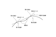
- the first peak is not limited to the portion observed as clearly showing the maximum. In the particle size distribution shown in FIG. 2, no obvious maximum is observed.
- the first peak is included in the first convex portion
- the second peak is included in the second convex portion. That is, the first convex portion is a shoulder-like portion having a common tangent to the apex of the second convex portion existing on the finer side than the second peak of the volume average particle size distribution.
- a first peak exists on the rough side near the contact point (first contact point) between the first convex portion and the tangent line, and the value of the particle size can be approximated by the particle size at the first contact point.
- the relationship between the particle size distribution and the common tangent line is as follows.
- the information on the scattered light intensity measured by the laser diffraction scattering method is Fourier transformed and given as a continuous distribution curve with the horizontal axis representing the particle diameter and the vertical axis representing the volume-based frequency.
- the maximum, minimum and inflection points can be specified by differentiating at least the first order of this distribution curve. That is, at the maximum and minimum, the first derivative value of the volume average particle size distribution is 0, and the maximum value corresponds to the particle size corresponding to the peak.
- the inflection point of the particle size distribution can be specified based on the results of the first and second derivative. Having a particle size distribution that can be evaluated as bimodal in this way means that the carbon material can be broadly classified into two types: a carbon material (a) having a large particle size and a carbon material (b) having a small particle size.
- the frequency of the current flowing in the carbon material passing through the SEI film can be reduced by the carbon material constituting the second peak having a large particle diameter, and the resistance in the carbon material can be reduced. As a result, it is possible to contribute to excellent characteristics of the electricity storage device in a low temperature environment. That is, first, a current network having a small number of passes through the SEI film is constituted by the carbon material constituting the second peak having a large particle diameter. And it is thought that the carbon material which comprises a finer 2nd peak or shoulder arrange
- FIG. 1 shows the case where a carbon material has a bimodal or a shoulder.
- FIG.1 (b) shows the case where a carbon material is a carbon material comprised by one peak. It is considered that the current flow path in the system shown in FIG. 1 (a) tends to be a conductive path that mainly passes through coarse particles.
- the bimodal carbon powder contains many fine carbon particles.
- the fine particles have a large surface area to volume ratio (specific surface area), and a large amount of such particles contributes to securing a sufficiently large surface area. Therefore, in the case of FIG. 1A, it is considered that the lithium moving interface between the carbon and the electrolyte can be made sufficiently large.
- a weak peak with a small particle size is recognized, and strictly speaking, it can be assumed that it can be evaluated as a so-called multimodal particle size distribution.
- multimodal means that three or more peaks are recognized. Even in such a case, it can be regarded as bimodal as long as it meets the above-mentioned purpose of the present invention.
- the first peak exists in a first range having a particle diameter of 0.01 ⁇ m or more and less than 1 ⁇ m, and the second peak has a particle diameter of 1 ⁇ m or more and 10 ⁇ m or less. It is preferable to control the particle size distribution so as to be in the range of 2. By controlling so as to obtain such a particle size distribution, the charge transfer resistance value can be further reduced. From the viewpoint of further reducing the charge transfer resistance value, the first peak is preferably included in a region of 0.2 ⁇ m or more and less than 1 ⁇ m, and included in a region of 0.5 ⁇ m or more and less than 0.7 ⁇ m. More preferably. From the same viewpoint, the second peak is more preferably included in a region of 1 ⁇ m or more and 5 ⁇ m or less.
- the abundance ratio (X) of the carbon material (a) included in the first range and the carbon material (b) included in the second range is 0.
- a range of 1 to 0.9 is preferable.
- the charge transfer resistance value can be further reduced.
- the range of X is more preferably 0.2 to 0.8, further preferably 0.2 to 0.6, and 0.3 to 0. .5 is most preferred.
- such a value of X can be calculated based on the following Equation 1.
- A represents the maximum frequency of appearance of the carbon material (a)
- B represents the maximum frequency of appearance of the carbon material (b).
- the abundance ratio is obtained at the maximum appearance frequency at each peak position.
- the frequency can be obtained by a laser diffraction scattering method using a laser diffraction particle size distribution system.
- the maximum appearance frequency is a value determined by a particle size distribution with the horizontal axis representing the logarithm of the particle size and the vertical axis representing the existence ratio. This particle size distribution can be obtained by dividing the cumulative particle size distribution into fixed intervals and displaying the ratio of the frequencies included in one interval as an abundance ratio.
- the component constituting the second peak and the component constituting the first peak are preferably obtained simultaneously by pulverizing the graphite material with a fluidized bed jet mill.
- the jet mill method include a collision plate jet mill, a swivel jet mill, and a fluidized bed jet mill.
- the fluidized bed type jet mill collides high-pressure air jetted from the opposing nozzle as an ultra-high-speed jet, supplies the particles to the area where the air current collides, and impacts the particles up to several ⁇ m order. It is a device that realizes crushing.
- This apparatus is also referred to as an airflow type pulverizer.
- the fluidized bed jet mill is a pulverization mechanism by collision between particles, it is considered that the pulverization is performed so that the surface of the particles is scraped. As the particle size becomes smaller, it becomes difficult to pulverize further unless energy sufficient to break the particles even if they collide with each other. For this reason, the carbon material subjected to jet mill pulverization is not easily pulverized, and the carbon material constituting the first peak is formed to correspond to a stable position in the particle size distribution.
- the fluidized bed jet mill is suitable as the jet mill system in the present embodiment, and by using this, the volume average particle size distribution is gradually reduced while gradually reducing the 50% volume cumulative diameter of the carbon material.
- the first peak can be formed at a substantially fixed position.
- a carbon material corresponding to the first peak in the volume average particle size distribution and a carbon material corresponding to the second peak can be obtained simultaneously. Since the particle diameter of the first peak is stable, it is considered that a carbon material having low resistance at a low temperature can be obtained without excessive grinding.
- the fluidized bed jet mill is pulverized while being repeatedly circulated in the pulverizer, it is unlikely to be excessively pulverized and a bimodal carbon material is likely to be obtained.
- a mechanical pulverizer that performs pulverization by friction with a large rigid body, grinding by impact, or the like, it is considered that fine particles are generated due to strong impact, and it is easy to form a broad particle size distribution. For this reason, it is considered that it is difficult to obtain a carbon material having a low resistance at low temperatures.
- the electrical storage device negative electrode which concerns on this form is equipped with the carbon material for electrical storage devices of this invention.
- the carbon material for an electricity storage device of the present invention of the present invention can exhibit a characteristic of reducing resistance at low temperatures. Therefore, the negative electrode for an electricity storage device of this embodiment to which this is applied can also exhibit the characteristics of reducing resistance at low temperatures.
- the electricity storage device includes the carbon material for an electricity storage device of the present invention or the electricity storage device negative electrode of the present invention.
- both of the carbon material for an electricity storage device of the present invention and the electricity storage device negative electrode of the present invention can exhibit the characteristics of reducing resistance at low temperatures. Therefore, the power storage device of this embodiment to which any of these is applied has reduced resistance even at low temperatures, and can exhibit excellent characteristics.
- the power storage device can be a lithium ion secondary battery or a lithium ion capacitor. By applying in this way, the charge transfer resistance value of the lithium ion secondary battery or the lithium ion capacitor can be reduced, and these output characteristics can be improved.
- the carbon material of the present invention having a low internal resistance can be suitably used.
- the carbon material for an electricity storage device is controlled to have a desired particle size distribution, charge transfer resistance can be reduced. And the output characteristic of these electrical storage devices can be improved by applying the said carbon material for electrical storage devices as negative electrodes for electrical storage devices, such as a negative electrode of a lithium ion secondary battery, and a negative electrode of a lithium ion capacitor.
- the method for producing a carbon material for an electricity storage device includes a step of pulverizing a graphite material using air as a medium using the fluidized bed jet mill described above.
- the function of the jet mill is as described above. That is, since a pulverization mechanism by collision of particles is adopted, pulverization is performed so that the surface of the particles is scraped. In addition, as the particle size decreases, it is difficult to pulverize further unless energy sufficient to destroy the particles even if they collide with each other. Hard to be crushed. Therefore, the carbon material which comprises a 1st peak is formed as a thing corresponding to the stable position in particle size distribution by the said process.
- the first peak can be formed at almost a fixed position of the volume average particle size distribution while gradually reducing the 50% volume cumulative diameter of the carbon material. That is, a carbon material corresponding to the first peak in the volume average particle size distribution and a carbon material corresponding to the second peak can be obtained simultaneously. Since the particle diameter of the first peak is stable, it is considered that a carbon material having low resistance at a low temperature can be obtained without excessive grinding. In addition, since the fluidized bed jet mill is pulverized while being repeatedly circulated in the pulverizer, it is unlikely to be excessively pulverized and a bimodal carbon material is likely to be obtained.
- natural graphite or artificial graphite can be employed as the graphite material.
- an isotropic graphite material containing amorphous coke as a raw material.
- An isotropic graphite material containing amorphous coke as a raw material includes a graphitization treatment in the manufacturing process, and thus has a feature of low impurity content.
- the raw material since the raw material includes an amorphous portion, the tendency to be crushed so that the surface of the particle is scraped is increased. Therefore, it is considered that it is difficult to overgrind and increase in resistance under a low temperature environment can be suppressed.
- An airflow classifier is a device that classifies powder by utilizing the difference between the force acting on the mass of powder particles and the force acting on the surface.
- the force acting on the mass of the powder particles utilizes centrifugal force, inertial force, gravity, and the like, and the force acting on the surface utilizes frictional force caused by airflow.
- classification is performed as follows. That is, a gas flow from the outside to the inside of the rotor rotating in the apparatus is formed.
- Coarse particles with a small specific surface area are separated to the outside of the rotor by centrifugal force, and micro particles with a large specific surface area ride on the airflow inside the rotor. Separated.
- there are methods such as increasing the rotational speed of the rotor to increase the action of the centrifugal force, and increasing the force acting on the powder surface by increasing the air flow.
- a method such as changing the pressure of compressed air on the pulverizer side can also be used. A plurality of these methods can be combined. However, it is not limited to these methods.
- the method for producing a carbon material for an electricity storage device includes a step of pulverizing a desired carbon material using a fluidized bed jet mill, the electricity storage device having a desired particle size distribution. Suitable for manufacturing carbon materials. That is, it is possible to manufacture a carbon material having a significantly reduced charge transfer resistance in a low temperature environment.
- artificial graphite was pulverized with air as a medium using a fluidized bed jet mill manufactured by Earth Technica.
- a classifier is integrated in the fluidized bed jet mill manufactured by Earth Technica.
- the classification point is adjusted by appropriately changing the rotor speed in the classifier, and the 10% volume cumulative diameter (D10), 50% volume cumulative diameter (D50), and 90% volume cumulative diameter (D90) are different from each other.
- Carbon materials of 1 to Example 4 and Comparative Examples 1 and 2 were prepared. These values are summarized in Table 1.
- the negative electrode slurry was applied to a solid surface weight of 1.0 g / cm 2 on one side of a 18 ⁇ m thick copper foil, and dried at 60 ° C. Each electrode was cut into a size of ⁇ 15 mm, and further vacuum-dried at 200 ° C. for 2 hours to produce negative electrodes according to Examples 1 to 4 and Comparative Examples 1 and 2.
- the negative electrode foil electrode and a counter electrode of ⁇ 15 mm and metal lithium having a thickness of 20 ⁇ m are arranged with a polyethylene separator having a thickness of 20 ⁇ m interposed, and the simulated cells according to Examples 1 to 4 and Comparative Examples 1 and 2 are arranged. Assembled.
- As an electrolytic solution to be injected into the simulation cell a solution in which LiPF 6 was dissolved so as to have a concentration of 1 mol / L with respect to a mixed solvent in which ethylene carbonate and diethyl carbonate were mixed at a weight ratio of 1: 1 was used. .
- the simulated cell was charged and discharged at 25 ° C. with an upper limit voltage of 2.0 V and a lower limit voltage of 0.01 V, and further charged and discharged with an upper limit voltage of 2.0 V and a lower limit voltage of 0.1 V. Then, the frequency was changed from 10 mHz to 1 MHz in an environment of ⁇ 30 ° C., and these cells were subjected to AC impedance measurement. Based on the measured AC impedance data, a complex plane display diagram (Cole-Cole plot) shown in FIG. 3 was created, and Rct in FIG. 3 was measured and calculated as a charge transfer resistance ( ⁇ ) at ⁇ 30 ° C. The results are also shown in Table 1.
- pulverization which concerns on each example, it used for the measurement using the laser diffraction type particle size distribution measuring apparatus (MT3300EX II; Nikkiso Co., Ltd. product), respectively.
- the measurement results are shown in FIG.
- the carbon materials according to Examples 1 to 3 were confirmed to have a minimum between the first peak and the second peak in each particle size distribution.
- the 1st peak which has a tangent common to a 2nd peak exists, and two inflection points exist between the contact points of a tangent, a 1st peak, and a 2nd peak. It was an existing particle size distribution.
- the first peak was included in the region of 0.01 ⁇ m or more and less than 1 ⁇ m
- the second peak was included in the region of 1 ⁇ m or more and 10 ⁇ m or less.
- Appearance frequencies B were determined and shown in Table 1.
- the abundance ratio X was calculated from the values of A and B based on the above formula 1, and the value of X was also shown in Table 1.
- FIG. 5 shows the relationship between the value of X and the charge transfer resistance value in each example and each comparative example.
- the cells of Examples 1 to 4 are recognized to be included in the range of 0.1 to 0.9 with the value of X calculated based on Equation 1 above. It was.
- the value of the charge transfer resistance is 6.3 to 7.95 k ⁇ , which is sufficiently reduced as the resistance value in a low temperature environment.
- Examples 1 to 3 have a minimum value between the first peak and the second peak.
- the value of the charge transfer resistance is 6.3 to 7.5 k ⁇ , and it can be seen that the value of the resistance in a low temperature environment is further reduced.
- Comparative Example 2 In contrast, in Comparative Example 2, the presence of the second peak was confirmed, but the presence of the first peak could not be confirmed. Further, the charge transfer resistance values of Comparative Example 1 and Comparative Example 2 were very high values of about 8.0 k ⁇ and 8.9 k ⁇ , respectively. That is, the resistance value in the low temperature environment of the cells according to these comparative examples has at least one second peak with the highest appearance frequency in the volume average particle size distribution and the first peak on the smaller particle size side. It was confirmed that the carbon material was higher than the carbon material of the example.
Landscapes
- Engineering & Computer Science (AREA)
- Chemical & Material Sciences (AREA)
- Power Engineering (AREA)
- Materials Engineering (AREA)
- Microelectronics & Electronic Packaging (AREA)
- Organic Chemistry (AREA)
- Inorganic Chemistry (AREA)
- General Chemical & Material Sciences (AREA)
- Electrochemistry (AREA)
- Chemical Kinetics & Catalysis (AREA)
- Manufacturing & Machinery (AREA)
- Life Sciences & Earth Sciences (AREA)
- General Life Sciences & Earth Sciences (AREA)
- Geology (AREA)
- Battery Electrode And Active Subsutance (AREA)
- Electric Double-Layer Capacitors Or The Like (AREA)
Description
なお、特許文献1に記載されているポリアセン系炭素材料は、フェノール樹脂等を炭化して得られる材料であり、他の炭素材料に対して比較的結晶性の悪い材料と評価されるものである。
一方、炭素材料の中でも黒鉛材料としては、コークス、ピッチなど易黒鉛化性炭素を原材料として高温で黒鉛化した人造黒鉛、天然資源として産出される天然黒鉛などが挙げられる。ポリアセン系物質と比較すると、これらの黒鉛材料は結晶性が高いため、劈開性が高く、微粉砕が困難であるといえる。さらに、当該黒鉛材料を粉砕して得られる粒子のアスペクト比が高いため、微粉砕し、低温での電荷移動抵抗を小さくすることによって上記ポリアセン系物質と同等の性能を発揮することは非常に困難であった。

黒鉛材料としては、コークス、ピッチなど易黒鉛化性材料を原材料として高温で処理した人造黒鉛、天然資源として産出される天然黒鉛などを挙げることができる。これらの黒鉛材料は、製鋼用電極、等方性黒鉛材など黒鉛関連産業で大量に生産され、加工粉など容易に入手可能である。また天然黒鉛は、天然資源として産出され、とくに熱処理など必要としないので容易に入手することができる。
ここで、10%体積累積径、50%体積累積径及び90%体積累積径は、例えば、一般的なレーザー回折散乱法により測定することができる。すなわち、10%体積累積径、50%体積累積径及び90%体積累積径とは、それぞれ、レーザー回折散乱法において体積粒子径の累積度数分布の10%、50%、90%を示す粒子径(直径)である。
リチウムイオンを電解質に用いた蓄電デバイスでは、炭素材料と電解質との界面でのリチウムイオンの移動をスムーズに行うため、炭素材料の表面積は大きいことが好ましく、粒子径は小さい方が好ましい。特に、50%体積累積径が4.0μm以下であると炭素材料の負極と電解質との界面におけるリチウムイオンの移動をスムーズに行うことができ、抵抗を小さくすることができる。
このようにして測定される50%体積累積径を4.0μm以下に制御することで、当該炭素材料の比表面積を十分に確保することができる。そのため、このような炭素材料を蓄電デバイスに適用すると、電荷移動抵抗を十分に低減することができる。なお、50%体積累積径が4.0μmを超える場合は、当該比表面積が減少し、電荷移動抵抗が増大する傾向がある。
10%体積累積径が、0.45μm未満であると、微小粒子が多くなり過ぎ、電極がかさ高くなるため、体積基準の蓄電容量が小さくなると推定される。10%体積累積径が、1.0μmを超えると、2つのピークが重なりバイモーダルな粒度分布を形成しにくくなると推定される。このような観点から、10%体積累積径の範囲を0.45以上かつ1.0μm以下とすることが望ましい。
90%体積累積径が、1.55μm未満であると、2つのピークが重なりバイモーダルな粒度分布を形成しにくくなると推定される。8.9μmを超えると、十分な比表面積が確保できず電荷移動抵抗が大きくなると推定される。このような観点から、90%体積累積径の範囲を1.8μm以上かつ6.0μm以下とすることが望ましい。
図1を参照して、バイモーダルの粒度分布を持つ本形態の炭素材料の電気的特徴を、シングルピークの粒度分布を持つ炭素材料と比較しながら説明する。図1(a)は、本発明に係るバイモーダルの粒度分布を持つ炭素材料を示し、図1(b)はシングルピークの粒度分布を持つ炭素材料である。
SEI膜は、炭素材料の表面に形成される。すなわち、細かく粉砕された炭素材料を採用することにより、負極を構成する炭素材料内を通過する電流のSEI膜を通過する頻度が増える。また、SEI膜の厚みは、炭素材料、電解質、温度などに依存する傾向はあるものの、炭素材料の粒子径とはほとんど無関係である。そのため、粒子径を小さくすると、炭素材料内を流れる電流のSEI膜を通過する頻度が増加することとなる。その結果、低温環境下での抵抗が高くなり、低温での性能劣化の原因となると考えられる。このため、50%体積累積径が十分に小さい場合は、これが小さくなるにつれて低温環境下での抵抗が増加する傾向がある。一方、50%体積累積径を0.8μm以上とすることで、炭素材料内部での低温での抵抗増加を抑制することができ、低温環境下での抵抗を低減することができると考えられる。
バイモーダルであるとは、すなわち、粒子径分布を解析した際、ピーク部分が少なくとも2箇所(第1のピークと、第2のピーク)認められることを意味する。ここでいう第1のピークとは、明らかに極大を示すものとして観察される部分に限定されない。図2に示す粒度分布では、明らかな極大が認められない。このような場合、第1のピークは第1の凸部に含まれ、第2のピークは、第2の凸部に含まれているものと評価する。
すなわち、体積平均粒子径分布の第2のピークより細かい側に存在する第2の凸部の頂点と共通の接線を有する肩状の部分が第1の凸部である。第1の凸部と前記接線との接点(第1の接点)の近傍粗い側に第1のピークが存在し、その粒子径の値は前記第1の接点における粒子径で近似できる。
粒子径分布と前記共通の接線との関係は、第1の接点で第1のピークと接した後、一旦分布曲線から離れ、凹部と接することなく第2の凸部における第2の接点で再度接する。このため、第1の接点と第2の接点との間には変曲点が少なくとも2カ所存在する。
なお、レーザー回折散乱法により測定された散乱光強度の情報は、フーリエ変換され、横軸を粒子径、縦軸を体積基準の頻度とする連続した分布曲線として与えられる。この分布曲線を少なくとも一階微分することで極大、極小及び変曲点を特定することができる。すなわち、極大、極小においては、体積平均粒子径分布の一階微分値が0となり、極大値はピークに対応する粒子径に相当する。さらに、一階微分及び二階微分の結果に基づき、粒子径分布の変曲点を特定することができる。このようにバイモーダルと評価できる粒子径分布を有することは、当該炭素材料を粒子径が大きい炭素材料(a)と小さい炭素材料(b)との2種類に大別できることを意味する。
上記効果について、図1に基づき、1つのピークで炭素材料が構成する場合と比較し説明する。図1(a)は、炭素材料が、バイモーダルあるいは肩を有する場合を示す。図1(b)は、炭素材料が、1つのピークで構成される炭素材料である場合を示す。
図1(a)に示す系における電流の流れる経路については、主に粗い粒子を経由する導電経路になりやすいものと考えられる。そのため、銅箔から離れた炭素粒子へ電流が流れるに際して、図1(b)の場合よりも図1(a)の場合の方が、電流がSEI膜を通過する回数が低減されるものと評価できる。したがって、図1(a)の場合は、銅箔から離れた炭素材料まで小さな抵抗で電流を流すことができると考えられる。
また、バイモーダルの炭素粉末の場合、細かな炭素粒子を多く含有している。細かな粒子は体積に対する表面積の比率(比表面積)が大きく、このような粒子を多く含むことにより、十分大きな表面積の確保に資する。したがって、図1(a)の場合の方が、炭素と電解質間のリチウムの移動する界面を十分に大きくすることができるものと考えられる。

ジェットミルの方式には、衝突板式ジェットミル、旋回式ジェットミル、流動層式ジェットミル等が挙げられる。これらの中で、流動層式ジェットミルは、対抗するノズルから噴射される高圧の空気を超高速ジェットとして衝突させ、粒子を気流の衝突する領域に供給し粒子どうしの衝撃によって数μmオーダーまでの粉砕を実現する装置である。当該装置は、気流式粉砕装置とも称されるものである。
上記の流動層式ジェットミルは、粒子同士の衝突による粉砕メカニズムであるので、粒子の表面が削られるように粉砕されると考えられる。粒子径が小さくなってくると、粒子同士が衝突しても破壊するほどのエネルギーが与えられなければそれ以上粉砕することは困難になる。このため、ジェットミル粉砕に供された炭素材料は過粉砕されにくく、第1のピークを構成する炭素材料は、粒子径分布中の安定した位置に対応するものとして形成される。
上記のとおり、本形態におけるジェットミルの方式としては、流動層式ジェットミルが適切であり、これを用いることで、炭素材料の50%体積累積径を徐々に細かくしながら、体積平均粒子径分布のほぼ定位置に、第1のピークを形成することができる。すなわち、体積平均粒子径分布における第1のピークに対応する炭素材料と、第2のピークに対応する炭素材料と、を同時に得ることができる。第1のピークの粒子径が安定しているので、過粉砕することなく、低温での抵抗の小さい炭素材料を得ることができると考えられる。
また、流動層式ジェットミルは、粉砕装置内で循環を繰り返しながら粉砕されるので過粉砕されにくく、バイモーダルの炭素材料が得られやすいと考えられる。
大きな剛体との摩擦、衝撃などによる摩砕等により粉砕を行う機械式粉砕装置では、衝撃が強いために微細な粒子が発生し、ブロードな粒度分布を形成しやすくなるものと考えられる。そのため、低温での抵抗の小さい炭素材料を得られにくいと考えられる。
次に、本形態に係る蓄電デバイス用炭素材料の製造方法について説明する。
上記ジェットミルの機能としては、前述したとおりである。すなわち、粒子同士の衝突による粉砕メカニズムを採用しているため、粒子の表面が削られるように粉砕が行われる。また、粒子径が小さくなってくると、粒子同士が衝突しても破壊するほどのエネルギーが与えられなければそれ以上粉砕することは困難になるため、ジェットミル粉砕に供された黒鉛材料は過粉砕されにくい。したがって、上記工程により、第1のピークを構成する炭素材料は、粒子径分布中の安定した位置に対応するものとして形成される。
また、上記ジェットミルを使用することで、炭素材料の50%体積累積径を徐々に細かくしながら、体積平均粒子径分布のほぼ定位置に、第1のピークを形成することができる。すなわち、体積平均粒子径分布における第1のピークに対応する炭素材料と、第2のピークに対応する炭素材料と、を同時に得ることができる。第1のピークの粒子径が安定しているので、過粉砕することなく、低温での抵抗の小さい炭素材料を得ることができると考えられる。
また、流動層式ジェットミルは、粉砕装置内で循環を繰り返しながら粉砕されるので過粉砕されにくく、バイモーダルの炭素材料が得られやすいと考えられる。
大きな剛体との摩擦、衝撃などによる摩砕等により粉砕を行う機械式粉砕装置では、衝撃が強いために微細な粒子が発生し、ブロードな粒度分布を形成しやすくなるものと考えられる。そのため、低温での抵抗の小さい炭素材料を得られにくいと考えられる。
得られる炭素材料を細かくするためには、ロータの回転数を早くして遠心力の作用を大きくする、気流を早くして粉体の表面に作用する力を大きくするなどの方法が挙げられる。さらに、粉砕機側の圧縮空気の圧力を変えるなどの方法を用いることもできる。なお、これらの方法を複数組み合わせることもできる。しかしながら、これらの方法に限定されるものではない。
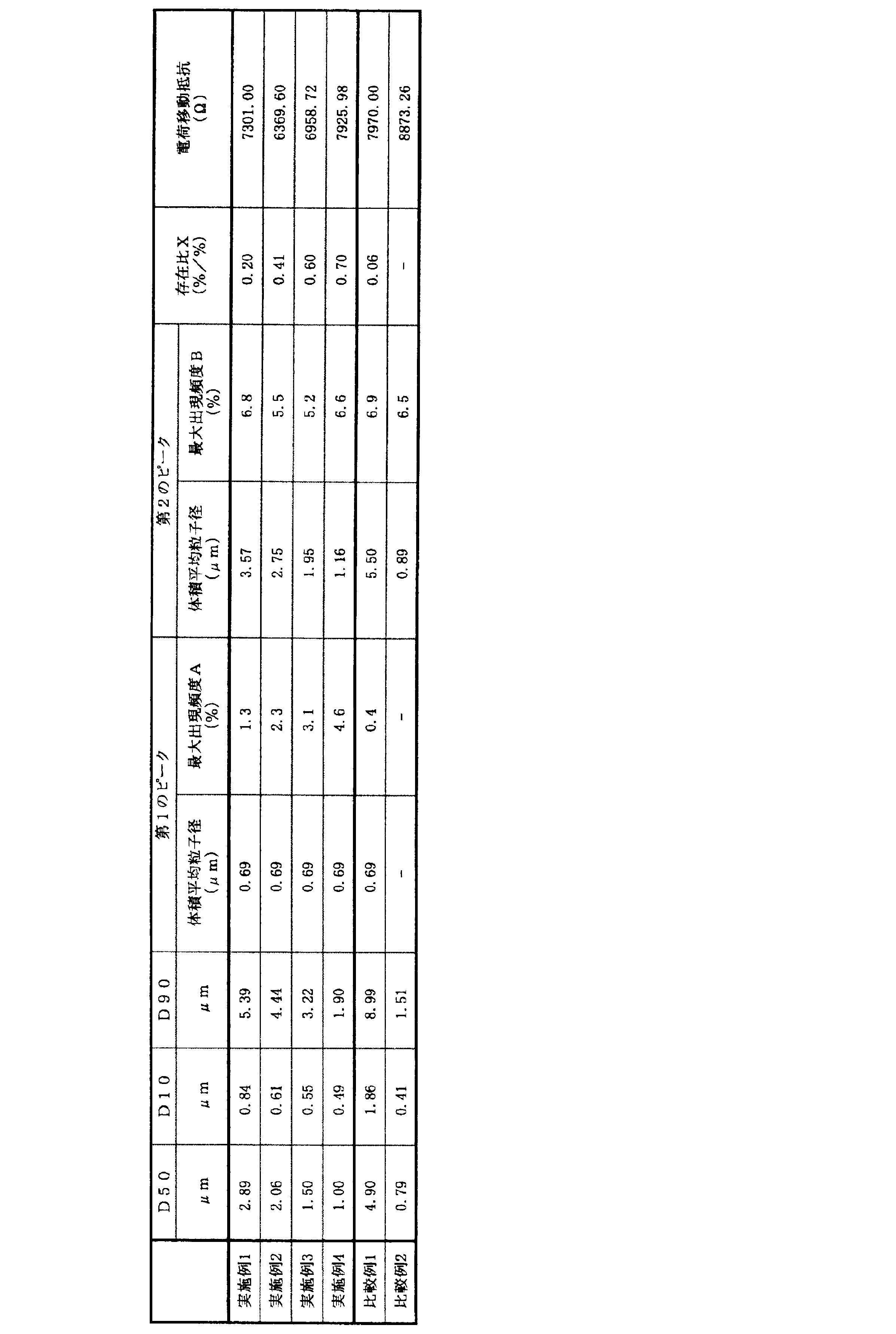
また、図4に示す体積平均粒子径分布において、実施例1~3は、第1のピークと第2のピークとの間に極小値を有することがわかる。さらに、実施例1~3は、電荷移動抵抗の値が6.3~7.5kΩとなっており、低温環境下における抵抗の値としてはさらに低減されていることがわかる。
これに対し、比較例2では、第2のピークの存在は確認されたが、第1のピークの存在は確認できなかった。また、比較例1、比較例2の電荷移動抵抗の値は、それぞれ約8.0kΩ、8.9kΩと非常に高い値が得られた。つまり、これら比較例に係るセルの低温環境下における抵抗の値は、体積平均粒子径分布において、少なくとも1つの出現頻度の最も高い第2のピークと、それより小さい粒子径側に第1のピークと、を有する実施例の炭素材料よりも高いことが確認された。
Claims (9)
- 黒鉛材料を粉砕してなる蓄電デバイス用炭素材料であって、
10%体積累積径が0.45μm以上かつ1.7μm以下であり、50%体積累積径が0.8μm以上かつ4.0μm以下であり、90%体積累積径が1.55μm以上かつ8.9μm以下であり、
体積平均粒子径分布が、出現頻度の最も高い第2のピークと、前記第2のピークよりも小さい粒子径側に位置する第1のピークと、を少なくとも有することを特徴とする蓄電デバイス用炭素材料。 - 前記第1のピークは粒子径0.01μm以上かつ1μm未満の第1の範囲に存在し、前記第2のピークは粒子径1μm以上かつ10μm以下の第2の範囲に存在することを特徴とする請求項1に記載の蓄電デバイス用炭素材料。
- 前記第1の範囲に含まれる炭素材料(a)と、前記第2の範囲に含まれる炭素材料(b)との存在比(X)を、下記数式1で求めた場合、0.1~0.9の範囲であることを特徴とする請求項2に記載の蓄電デバイス用炭素材料。

- 前記第2のピークを構成する成分と第1のピークを構成する成分は、黒鉛材料を流動層式ジェットミルで粉砕することにより同時に得られたことを特徴とする請求項1~3のいずれか一項に記載の蓄電デバイス用炭素材料。
- 請求項1~4のいずれか一項に記載の蓄電デバイス用炭素材料を備えることを特徴とする蓄電デバイス用負極。
- 請求項1~4のいずれか一項に記載の蓄電デバイス用炭素材料又は請求項5に記載の蓄電デバイス用負極を備えることを特徴とする蓄電デバイス。
- リチウムイオン二次電池又はリチウムイオンキャパシタであることを特徴とする請求項6に記載の蓄電デバイス。
- 請求項1~3のいずれか一項に記載の蓄電デバイス用炭素材料の製造方法であって、
黒鉛材料を流動層式ジェットミルで粉砕する工程を含むことを特徴とする蓄電デバイス用炭素材料の製造方法。 - 前記黒鉛材料として、アモルファスコークスを原材料として含む等方性黒鉛材料を用いることを特徴とする請求項8に記載の蓄電デバイス用炭素材料の製造方法。
Priority Applications (4)
| Application Number | Priority Date | Filing Date | Title |
|---|---|---|---|
| KR1020157011052A KR20150065773A (ko) | 2012-10-09 | 2013-10-07 | 축전 디바이스용 탄소 재료, 그의 제조 방법 및 그것을 사용한 축전 디바이스 |
| CN201380052575.1A CN104704587A (zh) | 2012-10-09 | 2013-10-07 | 蓄电器件用碳材料、其制造方法以及使用了该碳材料的蓄电器件 |
| US14/434,405 US20150270071A1 (en) | 2012-10-09 | 2013-10-07 | Carbon material for electrical storage device, method of manufacturing the same, and electrical storage device using the same |
| JP2014540839A JPWO2014057909A1 (ja) | 2012-10-09 | 2013-10-07 | 蓄電デバイス用炭素材料、その製造方法及びそれを用いた蓄電デバイス |
Applications Claiming Priority (2)
| Application Number | Priority Date | Filing Date | Title |
|---|---|---|---|
| JP2012224117 | 2012-10-09 | ||
| JP2012-224117 | 2012-10-09 |
Publications (1)
| Publication Number | Publication Date |
|---|---|
| WO2014057909A1 true WO2014057909A1 (ja) | 2014-04-17 |
Family
ID=50477376
Family Applications (1)
| Application Number | Title | Priority Date | Filing Date |
|---|---|---|---|
| PCT/JP2013/077253 Ceased WO2014057909A1 (ja) | 2012-10-09 | 2013-10-07 | 蓄電デバイス用炭素材料、その製造方法及びそれを用いた蓄電デバイス |
Country Status (5)
| Country | Link |
|---|---|
| US (1) | US20150270071A1 (ja) |
| JP (1) | JPWO2014057909A1 (ja) |
| KR (1) | KR20150065773A (ja) |
| CN (1) | CN104704587A (ja) |
| WO (1) | WO2014057909A1 (ja) |
Cited By (3)
| Publication number | Priority date | Publication date | Assignee | Title |
|---|---|---|---|---|
| CN104821233A (zh) * | 2015-04-03 | 2015-08-05 | 安徽江威精密制造有限公司 | 一种铜合金包覆秸秆基活性炭复合电极材料及其制备方法 |
| JPWO2021241420A1 (ja) * | 2020-05-26 | 2021-12-02 | ||
| JP2024034872A (ja) * | 2022-09-01 | 2024-03-13 | プライムアースEvエナジー株式会社 | 非水電解液二次電池の電極体及び非水電解液二次電池 |
Families Citing this family (4)
| Publication number | Priority date | Publication date | Assignee | Title |
|---|---|---|---|---|
| KR102088491B1 (ko) * | 2015-12-23 | 2020-03-13 | 주식회사 엘지화학 | 리튬 이차전지용 음극활물질 및 이를 포함하는 리튬 이차전지용 음극 |
| JP7471303B2 (ja) | 2018-12-19 | 2024-04-19 | ポスコホールディングス インコーポレーティッド | リチウム二次電池用負極活物質、及びその製造方法 |
| KR102240777B1 (ko) * | 2018-12-19 | 2021-04-14 | 주식회사 포스코 | 리튬 이차전지용 음극 활물질의 제조방법 |
| JP7584430B2 (ja) * | 2019-10-10 | 2024-11-15 | 株式会社クラレ | 電気化学デバイス用炭素質材料およびその製造方法、電気化学デバイス用負極、電気化学デバイス |
Citations (9)
| Publication number | Priority date | Publication date | Assignee | Title |
|---|---|---|---|---|
| JPH0482172A (ja) * | 1990-07-23 | 1992-03-16 | Yuasa Corp | リチウム電池 |
| JPH0831420A (ja) * | 1994-07-11 | 1996-02-02 | Osaka Gas Co Ltd | リチウム電池の電極用炭素材およびその製造方法 |
| JPH08227708A (ja) * | 1994-12-21 | 1996-09-03 | Ricoh Co Ltd | 電極および該電極を用いた二次電池 |
| JPH1145703A (ja) * | 1997-05-27 | 1999-02-16 | Tdk Corp | 非水電解質電池用電極 |
| JP2008103596A (ja) * | 2006-10-20 | 2008-05-01 | Fuji Heavy Ind Ltd | リチウムイオンキャパシタ |
| JP2009231234A (ja) * | 2008-03-25 | 2009-10-08 | Fuji Heavy Ind Ltd | 負極用炭素材料、蓄電デバイス、及び蓄電デバイス搭載品 |
| JP2010097830A (ja) * | 2008-10-16 | 2010-04-30 | Nippon Zeon Co Ltd | 電気化学素子用電極の製造方法 |
| JP2010114206A (ja) * | 2008-11-05 | 2010-05-20 | Hitachi Powdered Metals Co Ltd | リチウムイオンキャパシターの負極被膜及び電極被膜形成用塗料組成物 |
| WO2012121407A1 (ja) * | 2011-03-10 | 2012-09-13 | 株式会社クレハ | 非水電解質二次電池負極用炭素質材料 |
Family Cites Families (6)
| Publication number | Priority date | Publication date | Assignee | Title |
|---|---|---|---|---|
| JPH08153514A (ja) * | 1994-11-28 | 1996-06-11 | Ricoh Co Ltd | フィルム状非水電解液二次電池用負極および該電極を用いた非水電解液二次電池 |
| JP4120262B2 (ja) * | 2002-02-26 | 2008-07-16 | ソニー株式会社 | 非水電解質電池 |
| US20100047691A1 (en) * | 2006-10-25 | 2010-02-25 | Sumitomo Chemical Company, Limited | Lithium secondary battery |
| JP5292885B2 (ja) * | 2008-03-27 | 2013-09-18 | 住友化学株式会社 | 正極活物質粉末 |
| US8883564B2 (en) * | 2009-02-12 | 2014-11-11 | Denki Kagaku Kogyo Kabushiki Kaisha | Substrate comprising aluminum/graphite composite, heat dissipation part comprising same, and LED luminescent member |
| WO2012045002A1 (en) * | 2010-09-30 | 2012-04-05 | Energ2 Technologies, Inc. | Enhanced packing of energy storage particles |
-
2013
- 2013-10-07 JP JP2014540839A patent/JPWO2014057909A1/ja active Pending
- 2013-10-07 WO PCT/JP2013/077253 patent/WO2014057909A1/ja not_active Ceased
- 2013-10-07 KR KR1020157011052A patent/KR20150065773A/ko not_active Ceased
- 2013-10-07 CN CN201380052575.1A patent/CN104704587A/zh active Pending
- 2013-10-07 US US14/434,405 patent/US20150270071A1/en not_active Abandoned
Patent Citations (9)
| Publication number | Priority date | Publication date | Assignee | Title |
|---|---|---|---|---|
| JPH0482172A (ja) * | 1990-07-23 | 1992-03-16 | Yuasa Corp | リチウム電池 |
| JPH0831420A (ja) * | 1994-07-11 | 1996-02-02 | Osaka Gas Co Ltd | リチウム電池の電極用炭素材およびその製造方法 |
| JPH08227708A (ja) * | 1994-12-21 | 1996-09-03 | Ricoh Co Ltd | 電極および該電極を用いた二次電池 |
| JPH1145703A (ja) * | 1997-05-27 | 1999-02-16 | Tdk Corp | 非水電解質電池用電極 |
| JP2008103596A (ja) * | 2006-10-20 | 2008-05-01 | Fuji Heavy Ind Ltd | リチウムイオンキャパシタ |
| JP2009231234A (ja) * | 2008-03-25 | 2009-10-08 | Fuji Heavy Ind Ltd | 負極用炭素材料、蓄電デバイス、及び蓄電デバイス搭載品 |
| JP2010097830A (ja) * | 2008-10-16 | 2010-04-30 | Nippon Zeon Co Ltd | 電気化学素子用電極の製造方法 |
| JP2010114206A (ja) * | 2008-11-05 | 2010-05-20 | Hitachi Powdered Metals Co Ltd | リチウムイオンキャパシターの負極被膜及び電極被膜形成用塗料組成物 |
| WO2012121407A1 (ja) * | 2011-03-10 | 2012-09-13 | 株式会社クレハ | 非水電解質二次電池負極用炭素質材料 |
Cited By (5)
| Publication number | Priority date | Publication date | Assignee | Title |
|---|---|---|---|---|
| CN104821233A (zh) * | 2015-04-03 | 2015-08-05 | 安徽江威精密制造有限公司 | 一种铜合金包覆秸秆基活性炭复合电极材料及其制备方法 |
| JPWO2021241420A1 (ja) * | 2020-05-26 | 2021-12-02 | ||
| WO2021241420A1 (ja) * | 2020-05-26 | 2021-12-02 | パナソニックIpマネジメント株式会社 | 電気化学デバイス用電極および電気化学デバイス |
| US12051542B2 (en) | 2020-05-26 | 2024-07-30 | Panasonic Intellectual Property Management Co., Ltd. | Electrode for electrochemical devices, and electrochemical device |
| JP2024034872A (ja) * | 2022-09-01 | 2024-03-13 | プライムアースEvエナジー株式会社 | 非水電解液二次電池の電極体及び非水電解液二次電池 |
Also Published As
| Publication number | Publication date |
|---|---|
| JPWO2014057909A1 (ja) | 2016-09-05 |
| KR20150065773A (ko) | 2015-06-15 |
| CN104704587A (zh) | 2015-06-10 |
| US20150270071A1 (en) | 2015-09-24 |
Similar Documents
| Publication | Publication Date | Title |
|---|---|---|
| KR101987733B1 (ko) | 전고체 리튬이온 전지 | |
| CN102844269B (zh) | 改性天然石墨颗粒及其制造方法 | |
| CA3011539C (en) | Carbonaceous materials and methods of use thereof | |
| KR102087465B1 (ko) | 리튬 이차전지 음극재용 흑연분말의 제조방법 | |
| JPWO2014057909A1 (ja) | 蓄電デバイス用炭素材料、その製造方法及びそれを用いた蓄電デバイス | |
| KR102809883B1 (ko) | 비수계 이차 전지용 부극재, 비수계 이차 전지용 부극 및 비수계 이차 전지 | |
| JP5131429B2 (ja) | 非水電解質二次電池用負極及びその製造方法 | |
| JP6030995B2 (ja) | 非水電解質二次電池用負極材及びその製造方法並びにリチウムイオン二次電池 | |
| CN106654194A (zh) | 一种元素掺杂的SiOx负极复合材料及其制备方法和应用 | |
| JP6281306B2 (ja) | リチウムイオン二次電池用負極材、その製造方法、負極及びリチウムイオン二次電池 | |
| KR20150027167A (ko) | 리튬 이온 2차 전지용 음극 재료 | |
| CN107768669B (zh) | 球形石墨及其制备方法 | |
| JP6543428B1 (ja) | 二次電池用負極活物質および二次電池 | |
| JP2016001593A (ja) | 非水系電解液蓄電素子 | |
| CN106537662A (zh) | 二次电池用硅类活性物质粒子的制备方法及硅类活性物质粒子 | |
| JP2012216532A (ja) | 非水系二次電池用負極材料、これを用いた負極及び非水系二次電池 | |
| JP2008305661A (ja) | リチウムイオン二次電池用負極材とその製造方法 | |
| CN107195903B (zh) | 一种锂离子动力电池用小粒径天然石墨负极材料及其制备方法 | |
| CN103165869A (zh) | 改性中间相负极材料、锂离子二次电池及制备方法和应用 | |
| JP2015130324A (ja) | 非水電解液二次電池 | |
| TWI651883B (zh) | 鋰離子二次電池用負極材料及其製造方法、鋰離子二次電池用負極以及鋰離子二次電池 | |
| CN106165157A (zh) | 用于锂二次电池的负极活性材料的制造方法、和锂二次电池 | |
| JP2017112057A (ja) | シリコン系粒子およびそれを含むリチウムイオン二次電池用負極活物質並びにそれらの製造方法 | |
| JP2016178008A (ja) | リチウムイオン2次電池用負極活物質およびその製造方法 | |
| Idris et al. | Effects of polypyrrole on the performance of nickel oxide anode materials for rechargeable lithium-ion batteries |
Legal Events
| Date | Code | Title | Description |
|---|---|---|---|
| 121 | Ep: the epo has been informed by wipo that ep was designated in this application |
Ref document number: 13844750 Country of ref document: EP Kind code of ref document: A1 |
|
| ENP | Entry into the national phase |
Ref document number: 2014540839 Country of ref document: JP Kind code of ref document: A |
|
| NENP | Non-entry into the national phase |
Ref country code: DE |
|
| WWE | Wipo information: entry into national phase |
Ref document number: 14434405 Country of ref document: US |
|
| ENP | Entry into the national phase |
Ref document number: 20157011052 Country of ref document: KR Kind code of ref document: A |
|
| 122 | Ep: pct application non-entry in european phase |
Ref document number: 13844750 Country of ref document: EP Kind code of ref document: A1 |