WO2014057666A1 - 光結合素子およびこれを備えた光モジュール - Google Patents
光結合素子およびこれを備えた光モジュール Download PDFInfo
- Publication number
- WO2014057666A1 WO2014057666A1 PCT/JP2013/006015 JP2013006015W WO2014057666A1 WO 2014057666 A1 WO2014057666 A1 WO 2014057666A1 JP 2013006015 W JP2013006015 W JP 2013006015W WO 2014057666 A1 WO2014057666 A1 WO 2014057666A1
- Authority
- WO
- WIPO (PCT)
- Prior art keywords
- curvature
- light emitting
- optical
- optical coupling
- tolerance
- Prior art date
- Legal status (The legal status is an assumption and is not a legal conclusion. Google has not performed a legal analysis and makes no representation as to the accuracy of the status listed.)
- Ceased
Links
Images






Classifications
-
- G—PHYSICS
- G02—OPTICS
- G02B—OPTICAL ELEMENTS, SYSTEMS OR APPARATUS
- G02B6/00—Light guides; Structural details of arrangements comprising light guides and other optical elements, e.g. couplings
- G02B6/24—Coupling light guides
- G02B6/42—Coupling light guides with opto-electronic elements
- G02B6/4201—Packages, e.g. shape, construction, internal or external details
- G02B6/4204—Packages, e.g. shape, construction, internal or external details the coupling comprising intermediate optical elements, e.g. lenses, holograms
- G02B6/4214—Packages, e.g. shape, construction, internal or external details the coupling comprising intermediate optical elements, e.g. lenses, holograms the intermediate optical element having redirecting reflective means, e.g. mirrors, prisms for deflecting the radiation from horizontal to down- or upward direction toward a device
-
- G—PHYSICS
- G02—OPTICS
- G02B—OPTICAL ELEMENTS, SYSTEMS OR APPARATUS
- G02B6/00—Light guides; Structural details of arrangements comprising light guides and other optical elements, e.g. couplings
- G02B6/24—Coupling light guides
- G02B6/42—Coupling light guides with opto-electronic elements
- G02B6/4201—Packages, e.g. shape, construction, internal or external details
- G02B6/4249—Packages, e.g. shape, construction, internal or external details comprising arrays of active devices and fibres
- G02B6/425—Optical features
-
- G—PHYSICS
- G02—OPTICS
- G02B—OPTICAL ELEMENTS, SYSTEMS OR APPARATUS
- G02B6/00—Light guides; Structural details of arrangements comprising light guides and other optical elements, e.g. couplings
- G02B6/24—Coupling light guides
- G02B6/42—Coupling light guides with opto-electronic elements
- G02B6/4292—Coupling light guides with opto-electronic elements the light guide being disconnectable from the opto-electronic element, e.g. mutually self aligning arrangements
-
- G—PHYSICS
- G02—OPTICS
- G02B—OPTICAL ELEMENTS, SYSTEMS OR APPARATUS
- G02B6/00—Light guides; Structural details of arrangements comprising light guides and other optical elements, e.g. couplings
- G02B6/24—Coupling light guides
- G02B6/36—Mechanical coupling means
- G02B6/38—Mechanical coupling means having fibre to fibre mating means
- G02B6/3807—Dismountable connectors, i.e. comprising plugs
- G02B6/3873—Connectors using guide surfaces for aligning ferrule ends, e.g. tubes, sleeves, V-grooves, rods, pins, balls
- G02B6/3874—Connectors using guide surfaces for aligning ferrule ends, e.g. tubes, sleeves, V-grooves, rods, pins, balls using tubes, sleeves to align ferrules
- G02B6/3878—Connectors using guide surfaces for aligning ferrule ends, e.g. tubes, sleeves, V-grooves, rods, pins, balls using tubes, sleeves to align ferrules comprising a plurality of ferrules, branching and break-out means
-
- G—PHYSICS
- G02—OPTICS
- G02B—OPTICAL ELEMENTS, SYSTEMS OR APPARATUS
- G02B6/00—Light guides; Structural details of arrangements comprising light guides and other optical elements, e.g. couplings
- G02B6/24—Coupling light guides
- G02B6/36—Mechanical coupling means
- G02B6/38—Mechanical coupling means having fibre to fibre mating means
- G02B6/3807—Dismountable connectors, i.e. comprising plugs
- G02B6/3873—Connectors using guide surfaces for aligning ferrule ends, e.g. tubes, sleeves, V-grooves, rods, pins, balls
- G02B6/3885—Multicore or multichannel optical connectors, i.e. one single ferrule containing more than one fibre, e.g. ribbon type
-
- G—PHYSICS
- G02—OPTICS
- G02B—OPTICAL ELEMENTS, SYSTEMS OR APPARATUS
- G02B6/00—Light guides; Structural details of arrangements comprising light guides and other optical elements, e.g. couplings
- G02B6/24—Coupling light guides
- G02B6/42—Coupling light guides with opto-electronic elements
- G02B6/4201—Packages, e.g. shape, construction, internal or external details
- G02B6/4249—Packages, e.g. shape, construction, internal or external details comprising arrays of active devices and fibres
-
- G—PHYSICS
- G02—OPTICS
- G02B—OPTICAL ELEMENTS, SYSTEMS OR APPARATUS
- G02B6/00—Light guides; Structural details of arrangements comprising light guides and other optical elements, e.g. couplings
- G02B6/24—Coupling light guides
- G02B6/42—Coupling light guides with opto-electronic elements
- G02B6/4201—Packages, e.g. shape, construction, internal or external details
- G02B6/4255—Moulded or casted packages
Definitions
- the present invention relates to an optical coupling element and an optical module including the optical coupling element, and more particularly to an optical coupling element suitable for optically coupling a plurality of light emitting elements and end faces of a plurality of optical fibers, and a light including the same.
- modules for optically coupling a plurality of light emitting elements and end faces of a plurality of optical fibers, and a light including the same.
- this type of lens array could be attached with a photoelectric conversion device and a plurality of optical fibers each having a plurality of light emitting elements (for example, VCSEL, Vertical, Surface, Emitting, Laser).
- VCSEL Vertical, Surface, Emitting, Laser
- the lens array is optically coupled to the end face of each optical fiber with the light emitted from each light emitting element of the photoelectric conversion device in a state of being arranged between the photoelectric conversion device and the plurality of optical fibers. Multi-channel optical communication was possible.
- some of such lens arrays have a reflective surface on the light path of the light of the light emitting element, as shown in Patent Documents 1 to 3, for example.
- JP 2011-59484 A Japanese Patent Laid-Open No. 2001-51162 JP-A-9-281302
- the lens array has been mainly formed by an injection molding method of a resin material (for example, polyetherimide) using a mold.
- a resin material for example, polyetherimide
- such a lens array may be deformed (expanded) due to a temperature change due to heat generated by the laser itself or a temperature increase in a use environment that easily changes to a high temperature such as in a server.
- such a lens array may shrink at a low temperature than at a normal temperature.
- this type of lens array needs to maintain the optical coupling efficiency between the light emitting element and the end face of the optical fiber even when the deformation occurs, assuming deformation (thermal deformation) due to temperature change. It was.
- An object of the present invention is to provide an optical coupling element capable of effectively mitigating the temperature dependence of optical coupling efficiency while improving manufacturing efficiency and design freedom, and an optical module including the same.
- the present invention relates to the following optical coupling element and optical module.
- An optical coupling element configured to be capable of optically coupling the plurality of light emitting elements and end surfaces of the plurality of optical fibers in a state of being disposed between the plurality of light emitting elements and the plurality of optical fibers. And the light emitted from the plurality of light emitting elements is respectively incident on the first surface of the optical coupling element main body on the first light emitting element side corresponding to the plurality of light emitting elements.
- a plurality of incident surfaces having curvatures, and a second surface opposite to the first surface in the optical coupling element body, and arranged to have an inclination with respect to the first surface.
- a plurality of optical fibers A plurality of exit surfaces having curvatures, which are arranged so as to correspond to the end surfaces of the rivets, respectively, and emit light for each of the plurality of light emitting elements reflected by the reflecting surface toward the end surfaces of the plurality of optical fibers;
- the plurality of incident surfaces are aligned in the alignment direction of the single column so as to present only a single column, the alignment direction is defined as an “X direction”, and the plurality of light emission
- a traveling direction of light emitted from the element is defined as “Z direction”
- a direction perpendicular to the X direction and the Z direction is defined as “Y direction”
- the plurality of light emitting elements are defined as the plurality of optical fibers.
- each optical coupling efficiency with respect to the end face of each of the first and second end faces is moved from a position showing a preset maximum efficiency to a position where a decrease in the predetermined optical coupling efficiency with respect to the maximum efficiency is shown.
- the distance in the X direction between the position after movement is defined as “tolerance in the X direction”
- the distance in the Y direction between the position before movement and the position after movement is defined as “tolerance in Y direction”.
- the incidence surface, the reflection surface, and the emission surface are adjusted in curvature so that the tolerance in the X direction is larger than the tolerance in the Y direction.
- the plurality of incident surfaces are arranged in a state in which a plurality of unit rows in which a predetermined number or more of the incident surfaces are aligned are arranged in parallel along a parallel direction perpendicular to the alignment direction of the unit rows.
- the optical coupling element according to [1], wherein a direction having a relatively small angle with the virtual straight line is defined as an “X direction”.
- the plurality of incident surfaces are biconic surfaces convex toward the light emitting element such that the curvature in the X direction and the curvature in the Y direction are different from each other, and the reflection surface has a curvature in a YZ section.
- the plurality of incident surfaces are aspherical surfaces convex toward the light emitting element in which the curvature in the X direction and the curvature in the Y direction are the same, and the reflection surface has a curvature in a YZ cross section.
- the plurality of incident surfaces are assumed to be aspherical surfaces convex toward the light-emitting element in which the curvature in the X direction and the curvature in the Y direction are the same.
- the exit surface of the optical fiber is an aspherical surface convex toward the end face side of the optical fiber in which the curvature in the X direction and the curvature in the Y direction are the same.
- the tolerance when the reflection surface is assumed to be a plane
- the optical coupling element according to any one of [1] to [4], which has the same value and the curvature is adjusted to increase the tolerance in the X direction beyond this value.
- An optical module comprising the optical coupling element according to any one of [1] to [7] and a light emitting element.
- the temperature dependence of the optical coupling efficiency can be effectively reduced while improving the manufacturing efficiency and the degree of freedom of design.
- the tolerance in the X direction that easily affects the optical coupling efficiency due to thermal deformation can be made larger than the tolerance in the Y direction. it can. Therefore, the positional accuracy required for the light emitting element can be relaxed, and the temperature dependence of the optical coupling efficiency can be effectively relaxed while improving the manufacturing efficiency and the design freedom.
- the tolerance in the X direction can be positively improved as compared with the conventional case. For this reason, the positional accuracy required for the light emitting element can be more effectively relaxed.
- the reflecting surface can be configured only by the surface shape of the optical coupling element body. For this reason, it is possible to further improve the production efficiency by reducing the number of parts and the number of production steps.
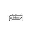
- FIG. 1 is a diagram illustrating a configuration of a lens array and an optical module as optical coupling elements according to the first embodiment.
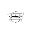
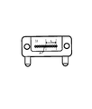
- FIG. 2 is a front view of the lens array.
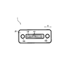
- FIG. 3 is a bottom view of the lens array.
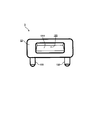
- FIG. 4 is a rear view of the lens array.
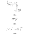
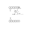
- 5A to 5C are schematic diagrams of the lens array.
- FIG. 6 is a schematic diagram showing a configuration of a conventional lens array.
- FIG. 7 is a diagram for explaining the effect of the first embodiment.
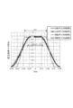
- FIG. 8 is a simulation result of tolerance using the lens array according to the first embodiment.
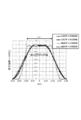
- FIG. 9 is a simulation result of tolerance using the lens array according to the second embodiment.
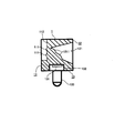
- FIG. 10 is a cross-sectional view of the lens array according to the third embodiment.
- FIG. 11 is a front view of the lens array.
- FIG. 12 is a bottom view of the lens array.
- FIG. 13 is a rear view of the lens array.
- FIG. 14 is a diagram for explaining the X direction in the third embodiment.
- FIG. 15 is a schematic diagram showing a modification of the third embodiment.
- FIG. 16 is a schematic diagram illustrating another modification of the third embodiment.
- FIG. 1 is a longitudinal sectional view (AA sectional view of FIG. 2) of a lens array (lens array body) 1 as an optical coupling element according to the first embodiment.
- FIG. 1 also shows an outline of an optical module 2 including a lens array 1.
- FIG. 2 is a front view of the lens array 1 shown in FIG.
- FIG. 3 is a bottom view of the lens array 1 shown in FIG.
- FIG. 4 is a rear view of the lens array 1 shown in FIG.
- the lens array 1 is disposed between the photoelectric conversion device 3 and the optical fiber 4.
- the lens array 1 optically couples the light emitting element 32 and the end face 41 of the optical fiber 4.
- the lens array 1 is integrally formed of a translucent resin material (for example, polyetherimide).
- the lens array 1 may be formed by, for example, an injection molding method.
- the photoelectric conversion device 3 includes a plurality of light emitting elements 32.
- the light emitting element 32 emits (emits) laser light L (see FIG. 5A) in a direction perpendicular to the surface of the semiconductor substrate 31 facing the lens array 1 (right direction in FIG. 1).
- the light emitting element 32 constitutes a vertical cavity surface emitting laser (VCSEL).
- the plurality of light emitting elements 32 are arranged in the direction perpendicular to the paper surface of FIG.
- the photoelectric conversion device 3 is disposed facing the lens array 1 so that the surface of the semiconductor substrate 31 on the lens array 1 side is in contact with the lens array 1.
- the photoelectric conversion device 3 is attached to the lens array 1 by a known fixing means.
- the optical fiber 4 is arranged in the same direction as the alignment direction of the light emitting elements 32 (the vertical direction in FIG. 1).
- the number of optical fibers 4 is the same as that of the light emitting elements 32.
- the plurality of optical fibers 4 are aligned with the plurality of light emitting elements 32 at the same pitch.
- the optical fiber 4 is attached to the lens array 1 by a known fixing means in a state where the portion on the end face 41 side is held in the multi-core collective connector 42.
- the optical fiber 4 may be a multimode fiber or a single mode fiber.
- the lens array 1 includes a plurality of first lens surfaces 111 (incident surfaces), total reflection surfaces 1211 (reflection surfaces), and a plurality of second lens surfaces 131. Have.
- the first lens surface 111 is disposed on the front end surface 11 (first surface) to which the photoelectric conversion device 3 (light emitting element 32) is attached.
- the number of first lens surfaces 111 is twelve, which is the same as that of the light emitting elements 32.
- a region (hereinafter, referred to as a first lens formation region) 112 where each first lens surface 111 is formed on the front end surface 11 is a first lens formation region 112 on the front end surface 11. This is the inner surface of the recess formed on the total reflection surface 1211 side with respect to the region other than.
- the first lens formation region 112 and other regions are planes parallel to each other. As shown in FIGS.
- the plurality of first lens surfaces 111 are in predetermined directions (perpendicular to the plane of FIG. 1, left and right in FIG. 2) so as to face the plurality of light emitting elements 32, respectively. Is arranged. Each first lens surface 111 is formed at the same pitch as the light emitting elements 32. Further, the central axis OA (1) (see FIG. 1) on each first lens surface 111 is a laser beam L (see FIG. 5) emitted from each light emitting element 32 corresponding to each first lens surface 111. ) Is preferably coincident with the optical axis.
- the total reflection surface 1211 is a reflection surface having a predetermined curvature.
- the total reflection surface 1211 is disposed on the rear end surface 12 (second surface) of the lens array 1.
- the total reflection surface 1211 is an inner bottom surface of a wedge-shaped recess 121 formed on the rear end surface 12. Further, the upper end portion of the total reflection surface 1211 is located closer to the photoelectric conversion device 3 than the lower end portion.
- the angle ⁇ of the total reflection surface 1211 with respect to the front end surface 11 (the smaller angle among the angles formed by the front end surface 11 and the straight line connecting the upper end portion and the lower end portion of the total reflection surface 1211).
- the tilt angle ⁇ ) may be 45 °.
- the second lens surface 131 (outgoing surface) has a predetermined curvature and is disposed on the lower end surface 13 (third surface) to which the optical fiber 4 is attached.
- the number of first lens surfaces 111 is twelve, which is the same as that of the light emitting elements 32.
- a region (hereinafter referred to as a second lens formation region) 132 in which each second lens surface 131 is formed on the lower end surface 13 is a second region on the lower end surface 13. This is the inner surface of the recess formed on the total reflection surface 1211 side of the outer region of the lens forming region 132.
- the second lens forming region 132 and the outer region are planes parallel to each other.
- the lower end surface 13 is adjacent to the front end surface 11 in a direction orthogonal to the arrangement direction of the first lens surface 111.
- the plurality of second lens surfaces 131 are arranged in the direction perpendicular to the paper surface of FIG. 1 (lateral direction in FIG. 3) corresponding to the end surfaces 41 of the plurality of optical fibers 4.
- the arrangement direction of the second lens surface 131 is the same as the arrangement direction of the first lens surface 111.
- the second lens surface 131 is formed at the same pitch as the first lens surface 111.
- the second lens surface 131 has the same position in the arrangement direction as the optically corresponding first lens surface 111.
- the central axis OA (2) (see FIG. 1) on each second lens surface 131 coincides with the central axis of the end surface 41 of each optical fiber 4 corresponding to each second lens surface 131. It is preferable.
- each light emitting element 32 is incident on each first lens surface 111.
- the laser light L is converged according to the power (refractive power) of the lens surface 111 and proceeds to the inside of the lens array 1.
- the incident laser light L reaches the total reflection surface 1211 at an incident angle larger than the critical angle.
- the laser beam L that has reached the total reflection surface 1211 is totally reflected toward the optical fiber 4 side (lower side).
- the light totally reflected by the total reflection surface 1211 reaches the second lens surface 131.
- the light that reaches the second lens surface 131 is emitted toward the end surface 41 of each corresponding optical fiber 4.
- each light emitting element 32 and the end face 41 of each optical fiber 4 are optically coupled via each first lens surface 111, total reflection surface 1211, and each second lens surface 131.
- the first lens surface 111, the total reflection surface 1211, and the second lens surface 131 have the same optical surface and different optical surfaces in order to make the tolerance in the X direction larger than the tolerance in the Y direction. Curvature adjustment is made in between.
- the “X direction” is defined as an alignment direction of a single row when a plurality of first lens surfaces 111 are arranged in a row as in the present embodiment (FIGS. 2 and 3). reference).
- the traveling direction of the laser light L of each light emitting element 32 in the lens array 1 is defined as “Z direction”.
- Z direction As shown in FIG. 5, in the present embodiment, since the optical path is bent at the total reflection surface 1211, the Z direction on the front end surface 11 and the Z direction on the lower end surface 13 are mutually different. Are different (orthogonal).
- Y direction is defined as a direction orthogonal to the X direction and the Z direction (see FIGS. 2 and 5).
- “Tolerance in the X direction” indicates the maximum efficiency in which the light coupling efficiencies of the plurality of light emitting elements 32 (in other words, the photoelectric conversion device 3) and the end faces 41 of the plurality of optical fibers 4 are set in advance.
- the position of the light emitting element 32 before the movement and the position of the light emitting element 32 after the movement in the case where it is assumed that the movement is made along the X direction from such a position to a position at which a decrease in the predetermined optical coupling efficiency with respect to the maximum efficiency is shown.
- the distance in the X direction is defined as
- “Tolerance in the Y direction” means that the light coupling efficiencies of the plurality of light emitting elements 32 (in other words, the photoelectric conversion device 3) with the end faces 41 of the plurality of optical fibers 4 exhibit the above-described maximum efficiency.
- the position of the light emitting element 32 before the movement and the position of the light emitting element 32 after the movement in the case where it is assumed that the light is moved along the Y direction from the position to a position where a predetermined decrease in the optical coupling efficiency with respect to the maximum efficiency is shown. It is defined as the distance in the Y direction.
- “tolerance in the Y direction” means that the plurality of first lens surfaces 111 are convex toward the light emitting element 32 side in which the curvature in the X direction and the curvature in the Y direction are the same.
- the plurality of second lens surfaces 131 are assumed to be aspherical surfaces convex toward the end face 41 side of the optical fiber 4 in which the curvature in the X direction and the curvature in the Y direction are the same.
- This is equivalent to the tolerance when the reflecting surface 1211 is assumed to be a plane. This value can be said to be the tolerance of a conventional lens array having a reflecting surface.
- the curvature adjustment is for positively increasing the tolerance in the X direction as compared with the conventional tolerance.
- the amount of decrease in the predetermined optical coupling efficiency serving as the tolerance criterion may be 18% ( ⁇ 1 dB) with respect to the maximum efficiency.
- each first lens surface 111 has a biconic surface convex toward the light emitting element 32 such that the curvature in the X direction and the curvature in the Y direction are different from each other. It is.
- the total reflection surface 1211 is a cylindrical surface that is concave with respect to the light emitting element 32 side and the end surface 41 of the optical fiber 4.
- Total reflection surface 1211 has a curvature in the YZ section (in other words, has a curved shape).
- the total reflection surface 1211 has no curvature in the XY cross section and the XZ cross section (in other words, has a linear shape).
- each second lens surface 131 is a cylindrical surface convex toward the end surface 41 side of the optical fiber 4.
- Each second lens surface 131 has a curvature in the XZ cross section, and does not have a curvature in the XY cross section and the YZ cross section.
- planar circular shapes are provided at both outer positions in the arrangement direction of the first lens surface 111 with respect to the first lens formation region 112 (that is, the X direction in the present embodiment).
- Each hole 113 is formed. These holes 113 are fitted to pins (not shown) formed on the semiconductor substrate 31 side, thereby mechanically positioning the photoelectric conversion device 3 when the photoelectric conversion device 3 is fixed to the lens array 1. Used.
- planar circular shapes are provided at both outer positions in the arrangement direction of the second lens surface 131 (X direction in the present embodiment) with respect to the second lens formation region 132.
- the pin 133 is erected.
- the pins 133 are used to mechanically position the optical fibers 4 in the lens array 1 by being inserted into holes (not shown) formed on the connector 42 side of the optical fibers 4.
- the first lens surface 111 is the biconic surface
- the total reflection surface 1211 is the cylindrical mirror surface having the main power in the YZ section
- the second lens surface 131 is the main in the XZ section.
- the lens array 1 according to Embodiment 1 can effectively mitigate the temperature dependence of the optical coupling efficiency while improving the manufacturing efficiency and the degree of freedom of design.
- the tolerance in the X direction is ⁇ (delta) X
- the tolerance in the Y direction is ⁇ Y
- the tolerance in the X direction in the lens array 1 according to the present embodiment is ⁇ X ′. If the tolerance in the Y direction is ⁇ Y ′, Equation (1) is established between these parameters.
- ⁇ is a linear expansion coefficient of the resin material forming the lens array 1
- ⁇ T is a temperature difference (for example, a difference between the temperature of the lens array 1 and room temperature).
- L is the distance in the X direction between a predetermined reference point (deformation center point) of thermal deformation of the lens array 1 on the front end surface 11 and the center point of the first lens surface 111 farthest from this reference point. .
- the thermal deformation reference point P that defines L is often the center point of the front end face 11.
- equation (3) is established between ⁇ X ′ and ⁇ L.
- equation (3) is solved for ⁇ T, equation (4) is obtained.
- the usable temperature range can be expanded as compared with the conventional case. According to the present embodiment, even when the temperature change of the lens array 1 is small or zero, the tolerance is widened, and the lens (1) is used without tightly positioning the device (such as VCSEL) and the fiber. be able to.
- ⁇ X ′ in Expression (5) is larger than ⁇ X of the conventional lens array, so the value L on the left side can be made larger than that of the conventional lens array.
- the number of channels (the number of the light emitting elements 32, the lens surfaces 111 and 131, and the optical fiber 4) can be increased as compared with the conventional case.
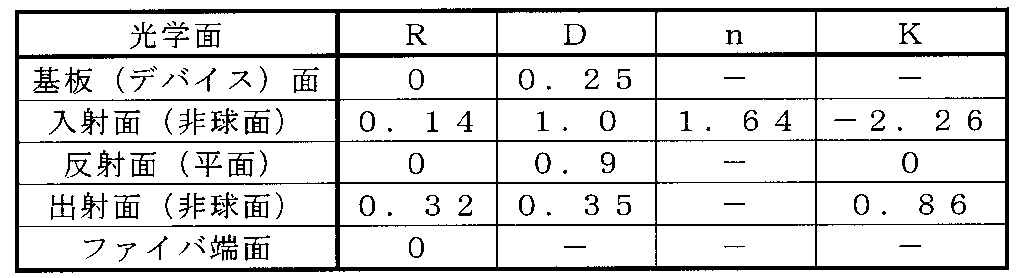
- Each parameter of the lens array 1 according to Embodiment 1 was set as shown in Table 1.
- R is the radius of curvature of the optical surface
- Rx is the radius of curvature (mm) in the X direction
- Ry is the radius of curvature (mm) in the Y direction.
- D is the distance (mm) to the next optical surface.
- n is the refractive index of the lens array 1 (resin material) corresponding to the operating wavelength of 850 nm.
- K is the conic coefficient of the optical surface
- Kx is the conic coefficient in the X direction
- Ky is the conic coefficient in the Y direction.
- FIG. 8 is a simulation result of tolerance using the first embodiment and a comparative lens array.
- the horizontal axis in FIG. 8 indicates the moving distance of the light emitting element 32.
- the vertical axis indicates the light coupling efficiency.
- FIG. 8 shows a case where the light emitting element 32 is moved along the X direction and the Y direction from the position where the maximum efficiency of the optical coupling efficiency is shown for each lens array of the first embodiment and the comparative example.
- the change in optical coupling efficiency is shown.
- the tolerances in the X direction and the Y direction can be obtained based on such a change characteristic of the optical coupling efficiency.
- the tolerance ⁇ X ′ in the X direction of the lens array 1 of the first embodiment was 1.5 times longer than the tolerance ⁇ X in the X direction of the lens array of the comparative example. Further, the tolerance ⁇ X ′ in the X direction is 1.5 times or more (that is, 1.2 times or more) longer than the tolerance ⁇ Y ′ in the Y direction.
- the tolerance is the amount of movement of the light emitting element 32 until the optical coupling efficiency decreases by only 5% with respect to the maximum efficiency.
- the tolerance standard is set strictly (to be reduced) in terms of optical performance, a significant improvement in tolerance is exhibited.
- Embodiment 2 Next, a lens array according to Embodiment 2 of the present invention will be described with reference to FIG. 9, focusing on differences from the lens array of Embodiment 1.
- the difference between the lens array 1 of the first embodiment and the lens array of the second embodiment is a mode of curvature adjustment of the first lens surface 111.
- the curvature in the X direction and the curvature in the Y direction on the first lens surface 111 are the same.
- the first lens surface 111 is an aspheric surface convex toward the light emitting element 32 side.
- the lens array according to the second embodiment can make the tolerance in the X direction larger than the tolerance in the Y direction, and can relax the positional accuracy required for the light emitting element 32.
- a tolerance simulation was performed using the lens arrays of the second embodiment and the comparative example in which each parameter was set to a predetermined value.
- the result of the simulation is shown in FIG.
- the horizontal axis in FIG. 9 indicates the moving distance of the light emitting element 32.
- the vertical axis indicates the light coupling efficiency.
- the tolerance ⁇ X ′ in the X direction of the lens array 1 of the second embodiment is 1.5 times the tolerance ⁇ X in the X direction of the lens array of the comparative example. It was long. Further, the tolerance ⁇ X ′ in the X direction was 1.5 times longer than the tolerance ⁇ Y ′ in the Y direction. Also in the second embodiment, the amount of movement of the light emitting element 32 until the decrease in the optical coupling efficiency with respect to the maximum efficiency is only 5% is set as the tolerance. However, it has been found that even when the tolerance standard is set strictly (to be reduced) in terms of optical performance, a significant improvement in tolerance is exhibited.
- FIG. 10 a lens array 1 according to Embodiment 3 of the present invention will be described with reference to FIGS. 10 to 15 with a focus on differences from the lens array 1 according to Embodiment 1.
- FIG. 10 a lens array 1 according to Embodiment 3 of the present invention
- FIG. 10 is a longitudinal sectional view (BB sectional view of FIG. 11) of the lens array 1 in the present embodiment.
- FIG. 11 is a front view of the lens array 1 shown in FIG.
- FIG. 12 is a bottom view of the lens array 1 shown in FIG.
- FIG. 13 is a rear view of the lens array 1 shown in FIG.
- FIG. 14 is a diagram for explaining the X direction in the third embodiment.
- FIG. 15 is a schematic diagram showing a modification of the third embodiment.
- the first lens surfaces 111 of the lens array 1 according to Embodiment 3 are arranged in two rows in parallel.
- the second lens surface 131 is a cylinder surface having a size corresponding to each of the first lens surfaces 111 in each row.
- the total reflection surface 1211 is a cylinder mirror surface having two types of curvature corresponding to the first lens surface 111 of each row.
- the light emitting elements 32 and the optical fibers 4 are arranged in two rows so as to correspond to the configuration of the lens array 1.
- the arrangement direction of the lens rows is defined as the direction in which the influence on the optical coupling efficiency due to thermal deformation is most likely to occur Defined as direction.
- Embodiment 3 a unit row in which a plurality of (for example, three) first lens surfaces 111 are arranged in a parallel direction orthogonal to the arrangement direction of the unit rows (the horizontal direction in FIG. 14).
- the “X direction” is defined as follows.
- the reference point P for thermal deformation of the lens array 1 on the front end surface 11 and the center point O of the first lens surface 111 farthest from the reference point P in the arrangement direction and the parallel direction are used.
- the direction in which the angle formed with the connecting virtual straight line l is relatively small is defined as the “X direction”.
- the angle formed by the alignment (lateral) direction and the virtual straight line 1 is ⁇ 1
- the angle formed by the parallel (vertical) direction and the virtual straight line 1 is ⁇ 2
- ⁇ 1 Is smaller.
- the horizontal direction in FIG. 14 is defined as the X direction and the vertical direction is defined as the Y direction.
- the curvature adjustment of the optical surfaces 111, 1211, and 131 as described above was performed in order to make the tolerance in the X direction larger than the tolerance in the Y direction.
- the direction that is most likely to be affected by thermal deformation is defined as the X direction. Also in this case, since the tolerance in the X direction can be made larger than the tolerance in the Y direction, it is possible to flexibly cope with diversification of the arrangement mode of the light emitting elements 32.
- the first lens surface 111 when the first lens surface 111 is aligned and arranged in a plurality of rows when viewed along any of a plurality of directions, such as a grid, for example, in the plurality of directions.
- a plurality of directions such as a grid
- the direction in which the number of alignments of the first lens surfaces 111 is the largest may be defined as the alignment direction, and the direction orthogonal thereto may be defined as the parallel direction, and the “X direction” may be determined.
- first lens surfaces 111 when the number of first lens surfaces 111 is small and a unit row in which a predetermined number (for example, three) or more of first lens surfaces 111 are aligned cannot be considered.
- line segment directions (broken lines in the figure) connecting the center points of the first lens surfaces 111, the thermal deformation reference point P and the center point O of the first lens surface 111 farthest from the reference point P
- the direction of the line segment in which the angle formed by the line segment l connecting the two and the line segment l is the minimum ( ⁇ 1 in the figure) may be defined as the “X direction”.
- optical coupling element and the optical module according to the present invention are useful for optical communication using an optical fiber, for example.
Landscapes
- Physics & Mathematics (AREA)
- General Physics & Mathematics (AREA)
- Optics & Photonics (AREA)
- Optical Couplings Of Light Guides (AREA)
Description
図1は、実施の形態1に係る光結合素子としてのレンズアレイ(レンズアレイ本体)1の縦断面図(図2のA-A断面図)である。図1では、レンズアレイ1を備えた光モジュール2の概要も示している。図2は、図1に示すレンズアレイ1の正面図である。図3は、図1に示すレンズアレイ1の底面図である。図4は、図1に示すレンズアレイ1の背面図である。
光電変換装置3は、複数の発光素子32を有する。発光素子32は、半導体基板31におけるレンズアレイ1に臨む面に対して垂直方向(図1における右方向)にレーザ光L(図5A参照)を出射(発光)する。発光素子32は、垂直共振器面発光レーザ(VCSEL:Vertical Cavity Surface Emitting Laser)を構成している。なお、複数の発光素子32は、図1の紙面垂直方向に配置されている。光電変換装置3は、例えば、半導体基板31のレンズアレイ1側の面がレンズアレイ1に当接するように、レンズアレイ1に対して対向して配置されている。そして、光電変換装置3は、公知の固定手段によってレンズアレイ1に取り付けられている。
光ファイバ4は、各発光素子32の整列方向と同じ方向(図1の紙面垂直方向)に配置されている。光ファイバ4の数は、発光素子32と同じである。複数の光ファイバ4は、複数の発光素子32と同一ピッチで整列されている。光ファイバ4は、端面41側の部位が多芯一括型のコネクタ42内に保持された状態で、公知の固定手段によってレンズアレイ1に取り付けられている。
第1のレンズ面111は、光電変換装置3(発光素子32)が取り付けられる前端面11(第1の面)上に配置されている。本実施の形態では、第1のレンズ面111の数は、発光素子32と同じ12個である。図1に示されるように、前端面11における各第1のレンズ面111が形成された領域(以下、第1のレンズ形成領域と称する)112は、前端面11における第1のレンズ形成領域112以外の領域よりも全反射面1211側に形成された凹部の内面である。また、第1のレンズ形成領域112とこれ以外の領域とは、互いに平行な平面である。図1および図2に示されるように、複数の第1のレンズ面111は、複数の発光素子32にそれぞれ対向するように、所定の方向(図1の紙面垂直方向、図2の左右方向)に配置されている。また、各第1のレンズ面111は、発光素子32と同一ピッチで形成されている。さらに、各第1のレンズ面111上の中心軸OA(1)(図1参照)は、各第1のレンズ面111にそれぞれ対応する各発光素子32から発光されるレーザ光L(図5参照)の光軸に一致していることが好ましい。
図1および図4に示されるように、全反射面1211は、所定の曲率を有する反射面である。全反射面1211は、レンズアレイ1の後端面12(第2の面)上に配置されている。全反射面1211は、後端面12に形成された楔状の凹部121の内底面である。また、全反射面1211の上端部は、下端部よりも光電変換装置3側に位置している。なお、図5Aに示されるように、前端面11に対する全反射面1211の傾斜角θ(前端面11と、全反射面1211の上端部と下端部とを結ぶ直線とがなす角度のうち小さい角度;傾斜角θ)は、45°であってもよい。
第2のレンズ面131(出射面)は、所定の曲率を有しており、光ファイバ4が取り付けられる下端面13(第3の面)上に配置されている。本実施の形態では、第1のレンズ面111の数は、発光素子32と同じ12個である。なお、図1および図3に示されるように、下端面13における各第2のレンズ面131が形成された領域(以下、第2のレンズ形成領域と称する)132は、下端面13における第2のレンズ形成領域132の外側の領域よりも全反射面1211側に形成された凹部の内面である。また、第2のレンズ形成領域132と外側の領域とは、互いに平行な平面である。下端面13は、前端面11に対して第1のレンズ面111の配置方向に直交する方向において隣接している。
本実施の形態において、第1のレンズ面111、全反射面1211および第2のレンズ面131は、X方向のトレランスをY方向のトレランスよりも大きくするために、同一光学面内および異光学面間において曲率調整がされている。
また、図2に示されるように、第1のレンズ形成領域112に対して第1のレンズ面111の配置方向(すなわち、本実施形態におけるX方向)における両外側位置には、平面円形状の穴部113がそれぞれ形成されている。これらの穴部113は、半導体基板31側に形成されたピン(図示省略)に嵌合することによって、レンズアレイ1に光電変換装置3を固定する際の光電変換装置3の機械的な位置決めに用いられる。
本実施形態によれば、上述したように、第1のレンズ面111をバイコーニック面、全反射面1211をYZ断面において主たるパワーを持つシリンドリカルミラー面、第2のレンズ面131をXZ断面において主たるパワーを持つシリンドリカル面とする。これにより、熱変形による光結合効率への影響が出やすいX方向のトレランスを、Y方向のトレランスよりも大きく、かつ従来のトレランスに比べて積極的に向上させることができる。また、発光素子32に求められる位置精度を緩和することができる。
実施の形態1に係るレンズアレイ1の各パラメータを表1に示すとおりに設定した。表1のRは光学面の曲率半径であり、RxはX方向の曲率半径(mm)であり、RyはY方向の曲率半径(mm)である。また、表1において、Dは、次の光学面までの距離(mm)である。nは、使用波長850nmに対応するレンズアレイ1(樹脂材料)の屈折率である。Kは光学面のコーニック係数であり、KxはX方向のコーニック係数であり、KyはY方向のコーニック係数である。

次に、本発明の実施の形態2に係るレンズアレイについて、実施の形態1のレンズアレイとの差異を中心に、図9を参照して説明する。
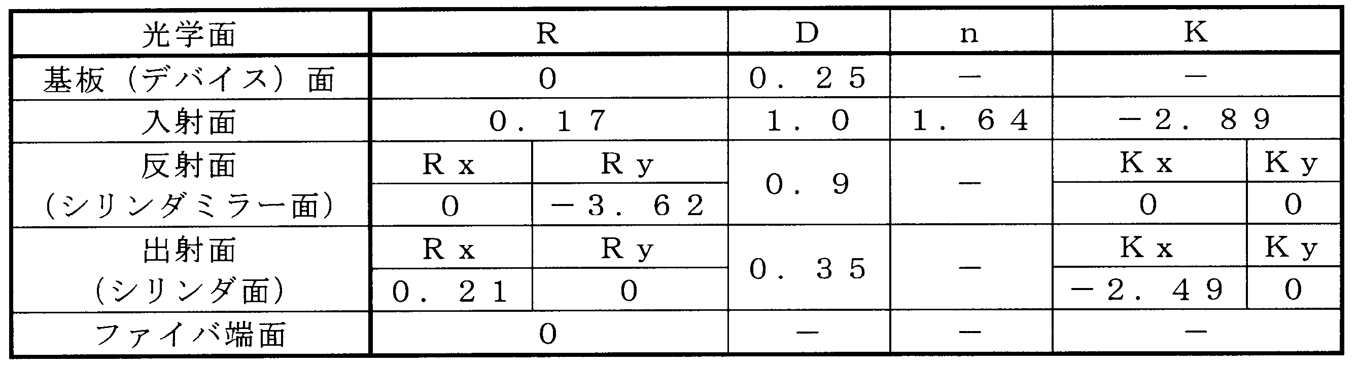
実施の形態2に係るレンズアレイ1の各パラメータを表3に示すとおりに設定した。表3におけるパラメータは、表1と同様である。また、比較例として用いた従来のレンズアレイは、実施の形態1と同じである。
次に、本発明の実施の形態3に係るレンズアレイ1について、実施の形態1に係るレンズアレイ1との差異を中心に、図10~図15を参照して説明する。
11 前端面
111 第1のレンズ面
12 後端面
1211 全反射面
13 下端面
131 第2のレンズ面
32 発光素子
4 光ファイバ
41 端面
Claims (8)
- 複数の発光素子と複数の光ファイバとの間に配置された状態で、前記複数の発光素子と前記複数の光ファイバの端面とをそれぞれ光学的に結合可能に構成された光結合素子であって、
光結合素子本体における前記複数の発光素子側の第1の面上に、前記複数の発光素子にそれぞれ対応して配置され、前記複数の発光素子から発光された光がそれぞれ入射する、曲率を有する複数の入射面と、
前記光結合素子本体における前記第1の面と反対側の第2の面上に、前記第1の面に対して傾きを有するように配置され、前記複数の入射面にそれぞれ入射した前記複数の発光素子ごとの光を前記複数の光ファイバ側に反射させる、曲率を有する反射面と、
前記光結合素子本体における前記複数の光ファイバ側の第3の面上に、前記複数の光ファイバの端面にそれぞれ対応するように配置され、前記反射面によって反射された前記複数の発光素子ごとの光を前記複数の光ファイバの端面に向けてそれぞれ出射させる、曲率を有する複数の出射面と
を備え、
前記複数の入射面が、単一列のみを呈するようにして前記単一列の整列方向に整列配置されている場合には、前記整列方向を「X方向」と定義し、
前記複数の発光素子から発光された光の進行方向を「Z方向」と定義し、
前記X方向および前記Z方向に直交する方向を「Y方向」と定義し、
前記複数の発光素子を、前記複数の光ファイバの端面とのそれぞれの光結合効率が予め設定された最大効率を示す位置から前記最大効率に対する所定の光結合効率の低下が示される位置まで移動させたと仮定した場合における移動前の位置と移動後の位置との間の前記X方向の距離を「X方向のトレランス」と定義し、
前記移動前の位置と前記移動後の位置との間の前記Y方向の距離を「Y方向のトレランス」と定義した場合、
前記入射面、前記反射面および前記出射面は、前記X方向のトレランスが前記Y方向のトレランスよりも大きくなるように曲率調整されている、
光結合素子。 - 前記複数の入射面が、所定数以上の前記入射面を整列させた単位列を、この単位列の整列方向に直交する並列方向に沿って複数列並列させた状態で配置されている場合、前記整列方向および前記並列方向のうち、前記第1の面上における前記光結合素子本体の熱変形の所定の基準点とこの基準点から最も離間された前記入射面の中心点とを結ぶ仮想直線とのなす角度が相対的に小さい方を、「X方向」と定義する、
請求項1に記載の光結合素子。 - 前記複数の入射面は、前記X方向の曲率と前記Y方向の曲率とが互いに異なるような前記発光素子側に凸のバイコーニック面であり、
前記反射面は、YZ断面において曲率を有するとともに、XY断面およびXZ断面において曲率を有しないような前記発光素子側および前記光ファイバの端面側に凹のシリンドリカル面であり、
前記複数の出射面は、XZ断面において曲率を有するとともに、XY断面およびYZ断面において曲率を有しないような前記光ファイバの端面側に凸のシリンドリカル面である、
請求項1または請求項2に記載の光結合素子。 - 前記複数の入射面は、前記X方向の曲率と前記Y方向の曲率とが互いに同一とされた前記発光素子側に凸の非球面であり、
前記反射面は、YZ断面において曲率を有するとともに、XY断面およびXZ断面において曲率を有しないような前記発光素子側および前記光ファイバの端面側に凹のシリンドリカル面であり、
前記複数の出射面は、XZ断面において曲率を有するとともに、XY断面およびYZ断面において曲率を有しないような前記光ファイバの端面側に凸のシリンドリカル面である、
請求項1または請求項2に記載の光結合素子。 - 前記Y方向のトレランスは、
前記複数の入射面を、前記X方向の曲率と前記Y方向の曲率とが互いに同一とされた前記発光素子側に凸の非球面と仮定し、
前記複数の出射面を、前記X方向の曲率と前記Y方向の曲率とが互いに同一とされた前記光ファイバの端面側に凸の非球面と仮定し、
前記反射面を平面と仮定した場合におけるトレランスと同値であり、この値よりも前記X方向のトレランスを大きくするための前記曲率調整がされている、
請求項1~4のいずれか1項に記載の光結合素子。 - 前記X方向のトレランスを前記Y方向のトレランスよりも1.2倍以上大きくするための前記曲率調整がされている、請求項1~5のいずれか1項に記載の光結合素子。
- 前記反射面は、前記複数の発光素子からの光を前記複数の出射面に向けてそれぞれ全反射させる全反射面である、請求項1~6のいずれか1項に記載の光結合素子。
- 請求項1~7のいずれか1項に記載の光結合素子と、
発光素子と、
を有する、光モジュール。
Priority Applications (3)
| Application Number | Priority Date | Filing Date | Title |
|---|---|---|---|
| CN201380052632.6A CN104755977B (zh) | 2012-10-10 | 2013-10-09 | 光耦合元件和具备该光耦合元件的光模块 |
| JP2014540744A JP6353366B2 (ja) | 2012-10-10 | 2013-10-09 | 光結合素子およびこれを備えた光モジュール |
| US14/434,332 US9389375B2 (en) | 2012-10-10 | 2013-10-09 | Optical coupling element and optical module provided with same |
Applications Claiming Priority (2)
| Application Number | Priority Date | Filing Date | Title |
|---|---|---|---|
| JP2012225197 | 2012-10-10 | ||
| JP2012-225197 | 2012-10-10 |
Publications (1)
| Publication Number | Publication Date |
|---|---|
| WO2014057666A1 true WO2014057666A1 (ja) | 2014-04-17 |
Family
ID=50477148
Family Applications (1)
| Application Number | Title | Priority Date | Filing Date |
|---|---|---|---|
| PCT/JP2013/006015 Ceased WO2014057666A1 (ja) | 2012-10-10 | 2013-10-09 | 光結合素子およびこれを備えた光モジュール |
Country Status (5)
| Country | Link |
|---|---|
| US (1) | US9389375B2 (ja) |
| JP (1) | JP6353366B2 (ja) |
| CN (1) | CN104755977B (ja) |
| TW (1) | TWI609206B (ja) |
| WO (1) | WO2014057666A1 (ja) |
Cited By (3)
| Publication number | Priority date | Publication date | Assignee | Title |
|---|---|---|---|---|
| WO2022144999A1 (ja) * | 2020-12-28 | 2022-07-07 | 株式会社エンプラス | 光レセプタクルおよび光モジュール |
| WO2022145001A1 (ja) * | 2020-12-28 | 2022-07-07 | 株式会社エンプラス | 光レセプタクルおよび光モジュール |
| JP2023084982A (ja) * | 2021-12-08 | 2023-06-20 | 株式会社エンプラス | 光レセプタクルおよび光モジュール |
Families Citing this family (7)
| Publication number | Priority date | Publication date | Assignee | Title |
|---|---|---|---|---|
| CN104755977B (zh) * | 2012-10-10 | 2016-08-24 | 恩普乐股份有限公司 | 光耦合元件和具备该光耦合元件的光模块 |
| US10175432B2 (en) * | 2014-11-18 | 2019-01-08 | Konica Minolta, Inc. | Optical path change element and optical coupling device |
| JP6621241B2 (ja) | 2015-02-02 | 2019-12-18 | 株式会社エンプラス | 光モジュール |
| JP2018087869A (ja) * | 2016-11-28 | 2018-06-07 | 株式会社エンプラス | 光モジュールおよび光モジュールの製造方法 |
| US10168494B2 (en) * | 2016-11-30 | 2019-01-01 | International Business Machines Corporation | Off-axis micro-mirror arrays for optical coupling in polymer waveguides |
| CN106597614A (zh) * | 2016-12-15 | 2017-04-26 | 武汉联特科技有限公司 | 单光口多路并行光接收耦合系统组件封装装置及其系统 |
| US10222555B2 (en) * | 2017-01-10 | 2019-03-05 | International Business Machines Corporation | Integrated optoelectronic chip and lens array |
Citations (3)
| Publication number | Priority date | Publication date | Assignee | Title |
|---|---|---|---|---|
| JP2001174671A (ja) * | 1999-12-16 | 2001-06-29 | Japan Aviation Electronics Industry Ltd | 光素子モジュール |
| JP2004302459A (ja) * | 2003-03-20 | 2004-10-28 | Sumitomo Electric Ind Ltd | 光モジュール |
| JP2012108443A (ja) * | 2010-10-28 | 2012-06-07 | Enplas Corp | レンズアレイおよびこれを備えた光モジュール |
Family Cites Families (17)
| Publication number | Priority date | Publication date | Assignee | Title |
|---|---|---|---|---|
| JPH05232359A (ja) * | 1992-02-26 | 1993-09-10 | Nippon Telegr & Teleph Corp <Ntt> | 平板マイクロレンズおよび平板マイクロレンズ付きファイバ |
| JP3537881B2 (ja) * | 1994-03-29 | 2004-06-14 | 株式会社リコー | Ledアレイヘッド |
| DE19610881B4 (de) * | 1995-12-07 | 2008-01-10 | Limo Patentverwaltung Gmbh & Co. Kg | Mikrosystembaustein |
| JPH09281302A (ja) | 1996-04-17 | 1997-10-31 | Nippon Sheet Glass Co Ltd | 反射面付き平板マイクロレンズアレイおよびその製造方法 |
| JP2001051162A (ja) * | 1999-06-04 | 2001-02-23 | Nippon Telegr & Teleph Corp <Ntt> | 光結合部品 |
| JP2001188151A (ja) * | 1999-10-18 | 2001-07-10 | Nippon Sheet Glass Co Ltd | 光モジュール |
| JP2003107295A (ja) * | 2001-09-28 | 2003-04-09 | Opnext Japan Inc | 光伝送モジュール |
| JP5050361B2 (ja) * | 2006-02-07 | 2012-10-17 | 富士ゼロックス株式会社 | 光コネクタ |
| US7850373B2 (en) * | 2007-03-12 | 2010-12-14 | Hitachi Cable, Ltd. | Optical block reinforcing member, optical block and optical module |
| JP2009020360A (ja) * | 2007-07-12 | 2009-01-29 | Mitsubishi Electric Corp | 光モジュール |
| CN201331603Y (zh) * | 2008-12-08 | 2009-10-21 | 王仲明 | 一种将多路半导体激光耦合入单根光纤的激光模块 |
| JP5238651B2 (ja) * | 2009-09-11 | 2013-07-17 | 株式会社フジクラ | 光路変更部材、光接続方法 |
| JP2011248312A (ja) * | 2010-04-26 | 2011-12-08 | Nippon Electric Glass Co Ltd | 光学素子及びそれを備える光学装置 |
| US9207413B2 (en) * | 2011-09-26 | 2015-12-08 | 3M Innovative Properties Company | Optical substrate having a plurality of staggered light redirecting features on a major surface thereof |
| JP2013235243A (ja) * | 2012-04-09 | 2013-11-21 | Fujikura Ltd | 光路変更部材 |
| WO2013180943A1 (en) * | 2012-05-29 | 2013-12-05 | 3M Innovative Properties Company | Optical interconnect |
| CN104755977B (zh) * | 2012-10-10 | 2016-08-24 | 恩普乐股份有限公司 | 光耦合元件和具备该光耦合元件的光模块 |
-
2013
- 2013-10-09 CN CN201380052632.6A patent/CN104755977B/zh active Active
- 2013-10-09 JP JP2014540744A patent/JP6353366B2/ja not_active Expired - Fee Related
- 2013-10-09 TW TW102136562A patent/TWI609206B/zh not_active IP Right Cessation
- 2013-10-09 WO PCT/JP2013/006015 patent/WO2014057666A1/ja not_active Ceased
- 2013-10-09 US US14/434,332 patent/US9389375B2/en active Active
Patent Citations (3)
| Publication number | Priority date | Publication date | Assignee | Title |
|---|---|---|---|---|
| JP2001174671A (ja) * | 1999-12-16 | 2001-06-29 | Japan Aviation Electronics Industry Ltd | 光素子モジュール |
| JP2004302459A (ja) * | 2003-03-20 | 2004-10-28 | Sumitomo Electric Ind Ltd | 光モジュール |
| JP2012108443A (ja) * | 2010-10-28 | 2012-06-07 | Enplas Corp | レンズアレイおよびこれを備えた光モジュール |
Non-Patent Citations (1)
| Title |
|---|
| TAKESHI SUGIU ET AL.: "Molded Glass Microlens Array for LD Array Module", IEICE TECHNICAL REPORT, vol. 93, no. 404, 17 December 1993 (1993-12-17), pages 49 - 54 * |
Cited By (6)
| Publication number | Priority date | Publication date | Assignee | Title |
|---|---|---|---|---|
| WO2022144999A1 (ja) * | 2020-12-28 | 2022-07-07 | 株式会社エンプラス | 光レセプタクルおよび光モジュール |
| JPWO2022144999A1 (ja) * | 2020-12-28 | 2022-07-07 | ||
| WO2022145001A1 (ja) * | 2020-12-28 | 2022-07-07 | 株式会社エンプラス | 光レセプタクルおよび光モジュール |
| US20240319452A1 (en) * | 2020-12-28 | 2024-09-26 | Enplas Corporation | Optical receptacle and optical module |
| JP2023084982A (ja) * | 2021-12-08 | 2023-06-20 | 株式会社エンプラス | 光レセプタクルおよび光モジュール |
| JP7846518B2 (ja) | 2021-12-08 | 2026-04-15 | 株式会社エンプラス | 光レセプタクルおよび光モジュール |
Also Published As
| Publication number | Publication date |
|---|---|
| US20150234135A1 (en) | 2015-08-20 |
| CN104755977B (zh) | 2016-08-24 |
| JPWO2014057666A1 (ja) | 2016-08-25 |
| US9389375B2 (en) | 2016-07-12 |
| JP6353366B2 (ja) | 2018-07-04 |
| TWI609206B (zh) | 2017-12-21 |
| TW201418813A (zh) | 2014-05-16 |
| CN104755977A (zh) | 2015-07-01 |
Similar Documents
| Publication | Publication Date | Title |
|---|---|---|
| JP6353366B2 (ja) | 光結合素子およびこれを備えた光モジュール | |
| US9223098B2 (en) | Lens array and optical module including the same | |
| CN103959122B (zh) | 光插座及具备该光插座的光模块 | |
| US9488790B2 (en) | Lens array and optical module including the same | |
| JP6289830B2 (ja) | 光レセプタクルおよび光モジュール | |
| CN108474912A (zh) | 光连接器和光传输模块 | |
| CN106104342B (zh) | 光插座和光模块 | |
| JP6747448B2 (ja) | 光路変換素子、光インターフェース装置、光伝送システム | |
| JP5737254B2 (ja) | 光通信モジュール | |
| JP6243568B1 (ja) | 光送受信用光学アセンブリー | |
| TWI596395B (zh) | Optical socket and its light module | |
| CN108508544B (zh) | 光耦合系统及光耦合方法 | |
| TWI608263B (zh) | Optical socket and light module with it | |
| EP2637052B1 (en) | Optical coupling structure and array optical amplification module | |
| WO2026094364A1 (ja) | 光結合部品 | |
| US20220082768A1 (en) | Optical module and optical connector cable | |
| JP6874596B2 (ja) | プリズム | |
| WO2022144999A1 (ja) | 光レセプタクルおよび光モジュール | |
| WO2026058583A1 (ja) | 光学システムおよび光コネクタ | |
| CN120703913A (zh) | 一种包含快轴光束整形的光学耦合微系统 | |
| CN120315076A (zh) | 光学系统以及激光雷达 | |
| CN113508323A (zh) | 光插座和光模块 |
Legal Events
| Date | Code | Title | Description |
|---|---|---|---|
| 121 | Ep: the epo has been informed by wipo that ep was designated in this application |
Ref document number: 13845628 Country of ref document: EP Kind code of ref document: A1 |
|
| ENP | Entry into the national phase |
Ref document number: 2014540744 Country of ref document: JP Kind code of ref document: A |
|
| WWE | Wipo information: entry into national phase |
Ref document number: 14434332 Country of ref document: US |
|
| NENP | Non-entry into the national phase |
Ref country code: DE |
|
| 122 | Ep: pct application non-entry in european phase |
Ref document number: 13845628 Country of ref document: EP Kind code of ref document: A1 |