WO2014054085A1 - 半導体デバイス、これを備えた近接センサーおよび半導体デバイスの製造方法 - Google Patents
半導体デバイス、これを備えた近接センサーおよび半導体デバイスの製造方法 Download PDFInfo
- Publication number
- WO2014054085A1 WO2014054085A1 PCT/JP2012/006439 JP2012006439W WO2014054085A1 WO 2014054085 A1 WO2014054085 A1 WO 2014054085A1 JP 2012006439 W JP2012006439 W JP 2012006439W WO 2014054085 A1 WO2014054085 A1 WO 2014054085A1
- Authority
- WO
- WIPO (PCT)
- Prior art keywords
- light
- semiconductor device
- receiving element
- light emitting
- light receiving
- Prior art date
- Legal status (The legal status is an assumption and is not a legal conclusion. Google has not performed a legal analysis and makes no representation as to the accuracy of the status listed.)
- Ceased
Links
Images



Classifications
-
- G—PHYSICS
- G01—MEASURING; TESTING
- G01V—GEOPHYSICS; GRAVITATIONAL MEASUREMENTS; DETECTING MASSES OR OBJECTS; TAGS
- G01V8/00—Prospecting or detecting by optical means
- G01V8/10—Detecting, e.g. by using light barriers
- G01V8/12—Detecting, e.g. by using light barriers using one transmitter and one receiver
-
- G—PHYSICS
- G01—MEASURING; TESTING
- G01S—RADIO DIRECTION-FINDING; RADIO NAVIGATION; DETERMINING DISTANCE OR VELOCITY BY USE OF RADIO WAVES; LOCATING OR PRESENCE-DETECTING BY USE OF THE REFLECTION OR RERADIATION OF RADIO WAVES; ANALOGOUS ARRANGEMENTS USING OTHER WAVES
- G01S17/00—Systems using the reflection or reradiation of electromagnetic waves other than radio waves, e.g. lidar systems
- G01S17/02—Systems using the reflection of electromagnetic waves other than radio waves
- G01S17/04—Systems determining the presence of a target
-
- G—PHYSICS
- G01—MEASURING; TESTING
- G01S—RADIO DIRECTION-FINDING; RADIO NAVIGATION; DETERMINING DISTANCE OR VELOCITY BY USE OF RADIO WAVES; LOCATING OR PRESENCE-DETECTING BY USE OF THE REFLECTION OR RERADIATION OF RADIO WAVES; ANALOGOUS ARRANGEMENTS USING OTHER WAVES
- G01S7/00—Details of systems according to groups G01S13/00, G01S15/00, G01S17/00
- G01S7/48—Details of systems according to groups G01S13/00, G01S15/00, G01S17/00 of systems according to group G01S17/00
- G01S7/481—Constructional features, e.g. arrangements of optical elements
- G01S7/4811—Constructional features, e.g. arrangements of optical elements common to transmitter and receiver
- G01S7/4813—Housing arrangements
-
- H—ELECTRICITY
- H10—SEMICONDUCTOR DEVICES; ELECTRIC SOLID-STATE DEVICES NOT OTHERWISE PROVIDED FOR
- H10F—INORGANIC SEMICONDUCTOR DEVICES SENSITIVE TO INFRARED RADIATION, LIGHT, ELECTROMAGNETIC RADIATION OF SHORTER WAVELENGTH OR CORPUSCULAR RADIATION
- H10F55/00—Radiation-sensitive semiconductor devices covered by groups H10F10/00, H10F19/00 or H10F30/00 being structurally associated with electric light sources and electrically or optically coupled thereto
- H10F55/20—Radiation-sensitive semiconductor devices covered by groups H10F10/00, H10F19/00 or H10F30/00 being structurally associated with electric light sources and electrically or optically coupled thereto wherein the electric light source controls the radiation-sensitive semiconductor devices, e.g. optocouplers
- H10F55/25—Radiation-sensitive semiconductor devices covered by groups H10F10/00, H10F19/00 or H10F30/00 being structurally associated with electric light sources and electrically or optically coupled thereto wherein the electric light source controls the radiation-sensitive semiconductor devices, e.g. optocouplers wherein the radiation-sensitive devices and the electric light source are all semiconductor devices
- H10F55/255—Radiation-sensitive semiconductor devices covered by groups H10F10/00, H10F19/00 or H10F30/00 being structurally associated with electric light sources and electrically or optically coupled thereto wherein the electric light source controls the radiation-sensitive semiconductor devices, e.g. optocouplers wherein the radiation-sensitive devices and the electric light source are all semiconductor devices formed in, or on, a common substrate
-
- H—ELECTRICITY
- H10—SEMICONDUCTOR DEVICES; ELECTRIC SOLID-STATE DEVICES NOT OTHERWISE PROVIDED FOR
- H10F—INORGANIC SEMICONDUCTOR DEVICES SENSITIVE TO INFRARED RADIATION, LIGHT, ELECTROMAGNETIC RADIATION OF SHORTER WAVELENGTH OR CORPUSCULAR RADIATION
- H10F77/00—Constructional details of devices covered by this subclass
- H10F77/40—Optical elements or arrangements
- H10F77/413—Optical elements or arrangements directly associated or integrated with the devices, e.g. back reflectors
-
- H—ELECTRICITY
- H10—SEMICONDUCTOR DEVICES; ELECTRIC SOLID-STATE DEVICES NOT OTHERWISE PROVIDED FOR
- H10W—GENERIC PACKAGES, INTERCONNECTIONS, CONNECTORS OR OTHER CONSTRUCTIONAL DETAILS OF DEVICES COVERED BY CLASS H10
- H10W74/00—Encapsulations, e.g. protective coatings
- H10W74/10—Encapsulations, e.g. protective coatings characterised by their shape or disposition
-
- H—ELECTRICITY
- H10—SEMICONDUCTOR DEVICES; ELECTRIC SOLID-STATE DEVICES NOT OTHERWISE PROVIDED FOR
- H10W—GENERIC PACKAGES, INTERCONNECTIONS, CONNECTORS OR OTHER CONSTRUCTIONAL DETAILS OF DEVICES COVERED BY CLASS H10
- H10W90/00—Package configurations
- H10W90/701—Package configurations characterised by the relative positions of pads or connectors relative to package parts
- H10W90/751—Package configurations characterised by the relative positions of pads or connectors relative to package parts of bond wires
- H10W90/754—Package configurations characterised by the relative positions of pads or connectors relative to package parts of bond wires between a chip and a stacked insulating package substrate, interposer or RDL
Definitions
- the object detection sensor portion of the opto-device includes a substrate, a light emitting element and a light receiving element mounted on the substrate, a light emitting element and a light receiving element sealed with a translucent resin, and a transmission lens facing the light emitting element and A mold part including a receiving lens facing the light receiving element; a groove formed between the transmitting lens and the receiving lens in the mold part; and a light shielding member provided in the groove and configured to shield light from the light receiving element. It is equipped with. Light emitted from the light emitting element and traveling through the mold portion toward the light receiving element is shielded by a light shielding member provided in the groove.
- an opto device semiconductor device having such a communication function is mounted on, for example, a portable terminal.
- the opto device in a portable terminal may be arrange
- the conventional optical device when the conventional optical device is disposed inside the panel body, the light traveling from the light emitting element to the light receiving element in the mold portion is shielded by the light shielding member, but is reflected by the panel body and is reflected on the light receiving element.
- the light that goes can not be shielded. That is, there is a problem that noise light reflected from the panel body cannot be prevented from noise light that travels from the light emitting element to the light receiving element.
- the present invention provides a semiconductor device capable of suppressing light reaching a light receiving element by being reflected from a panel body or the like from light that travels from the light emitting element to the light receiving element, a proximity sensor including the semiconductor device, and a method for manufacturing the semiconductor device The challenge is to do.
- the semiconductor device of the present invention is a semiconductor device formed by sealing a light emitting element and a light receiving element mounted on a common package substrate with a sealing resin, and the surface of the sealing resin is a light emitting element with respect to the package substrate. It is characterized by being formed with an inclined surface that is inclined downward from the light receiving element toward the light receiving element.
- the surface of the sealing resin is formed with an inclined surface inclined downward from the light emitting element toward the light receiving element, the light (detection light) emitted from the light emitting element is the surface of the sealing resin.
- the light In the (interface with air), the light is refracted to the side away from the light receiving element as a whole.
- the light that passes through the panel body on the light receiving element side out of the refracted light is incident on the panel body at a deep angle and its reflection is suppressed. That is, of the noise light that travels from the light emitting element to the light receiving element, it is possible to suppress the noise light that is reflected from the panel body and reaches the light receiving element.
- the “package substrate” is a concept including a lead frame.
- the light emitting element and the light receiving element are preferably sealed by potting a sealing resin.
- the package substrate is tilted by the angle of the inclined surface, and only the sealing resin is poured and cured, or after the sealing resin is poured, the package substrate is tilted and cured.
- a sealing resin having an inclined surface on the surface can be easily formed.
- At least one of the light emitting element and the light receiving element is mounted so as to be immersed in a concave groove formed in the package substrate.
- the emitted light is appropriately reflected in the groove and emitted from the opening side of the groove.
- the radiated light from a light emitting element has directivity, and does not reach a light receiving element as noise light.
- the efficiency of extracting emitted light from the light emitting element can be improved by the concave groove.
- the emitted light from the light emitting element toward the light receiving element passes through the opening, and therefore does not reach the light receiving element as noise light. Therefore, even in the sealing resin, the wraparound of light (noise light) from the light emitting element to the light receiving element can be suppressed.
- the proximity sensor of the present invention includes the semiconductor device described above, and is characterized by sensing the relative approach of an object through a translucent panel body.
- noise light incident on the light receiving element can be reduced by reflection from the panel body.
- wraparound of light (noise light) from the light emitting element to the light receiving element can be suppressed, and erroneous detection or the like can be effectively prevented.
- the panel body is mounted on the mobile terminal and the panel body is a touch panel of the mobile terminal.
- the semiconductor device manufacturing method of the present invention is a semiconductor device manufacturing method described above, in which a light emitting element and a light receiving element are chip-mounted on a package substrate on which a wiring pattern is formed, and after the mounting process, light emission is performed.
- a potting step of potting the light-emitting element and the light-receiving element with the sealing resin is a semiconductor device manufacturing method described above, in which a light emitting element and a light receiving element are chip-mounted on a package substrate on which a wiring pattern is formed, and after the mounting process, light emission is performed.
- the sealing resin having an inclined surface on the surface is easily formed simply by pouring the sealing resin into the package substrate maintained in a horizontal posture, and then curing the sealing resin by tilting the package substrate.
- a semiconductor device that can suppress the wraparound of light (noise light) from the light emitting element to the light receiving element simply by tilting the package substrate when curing the sealing resin can be easily achieved. Can be manufactured.
- the resin sealing is performed at the wafer level, it is preferable to provide a plate (frame plate) for each device row in the potting process.
- the potting process is performed at the wafer level, and the wafer has a slat provided at each dicing line position and a four-circumference frame provided at the four peripheral edges, and at least one end of each slat. It is preferable that the portion is bent in an “L” shape so as to be separated from the four-circumferential frame.
- the sealing resin can be uniformly and smoothly poured over the entire wafer. Moreover, the thickness and inclination angle of the sealing resin in the semiconductor device after being separated (dicing) can be made the same.
- This semiconductor device includes a light emitting element and a light receiving element, and is used as a proximity sensor.
- this proximity sensor is mounted on a portable terminal (smart phone) and detects whether or not the user is talking. For this reason, in order to reliably receive the weak reflected light reflected from the human body, the light is prevented from wrapping around from the light emitting element to the light receiving element as much as possible.
- the amount of received light (current value) is compared with a threshold, and when the threshold is exceeded, the human body (ear E) is detected, that is, the call state is detected. Then, when a call state is detected, mode switching that disables the operation of the touch panel 2 is performed.
- the proximity sensor 5 detects an extremely close target (ear E or the like), the light emission amount is suppressed to reduce power consumption, and the light reception amount is extremely small compared to the light emission amount. Must be detected reliably. Therefore, the semiconductor device 10 of the present embodiment constituting the proximity sensor 5 is configured to reduce noise light as much as possible in order to improve the S / N ratio.
- FIG. 2 is a cross-sectional view of the semiconductor device 10A according to the first embodiment.
- the semiconductor device 10A includes a package substrate 11 composed of a substrate frame and a lead frame (a substrate frame in the embodiment), a light emitting element 12 and a light receiving element having a chip configuration mounted on the package substrate 11. 13 and a translucent sealing resin 14 that seals the light emitting element 12 and the light receiving element 13.
- the light receiving element 13 is mounted (mounted) on the package substrate 11, while the light emitting element 12 is mounted in a concave groove 15 formed in the package substrate 11.
- the surface 14a of the sealing resin 14 is an inclined surface, and faces the touch panel 2 (panel body) with an inclined gap.
- the package substrate 11 (substrate frame) is made of a glass epoxy or organic material substrate, and on both the front and back surfaces, a light emitting side wiring pattern 21 (electrodes and the like) on which the light emitting element 12 is mounted and conducted, and a light receiving element Light receiving side wiring patterns 22 (electrodes and the like) on which 13 is mounted and conducted are formed. Further, an inverted frustoconical groove 15 is formed in a portion of the package substrate 11 where the light emitting element 12 is mounted. The light emitting element 12 is mounted on a light emitting side wiring pattern 21 (die pad) that also serves as a heat sink provided on the groove bottom 15a of the concave groove 15. A reflective film is preferably formed on the inner peripheral surface of the concave groove 15.
- the light emitting element 12 is composed of a light emitting diode chip that emits infrared rays (near infrared rays) from the light emitting surfaces at both ends. And the electrode pad 12a of the light emitting element 12 and the land 21a of the light emission side wiring pattern 21 are connected by the bonding wire 24 (a gold wire, a copper wire, an aluminum wire, etc.).
- the light emitting element 12 is disposed so as to be completely immersed in the groove 15 formed in the package substrate 11.
- the light emitting element 12 may have a light emitting surface on the top surface.
- infrared light is reflected from the both ends of the small edge to the inner surface of the groove 12 and emitted from the opening.
- the infrared rays used as detection light are radiated with the radiation angle narrowed down (focused) and directivity.
- the reflection of infrared rays on the upper surface (interface with air) of the sealing resin 14 and the lower surface (interface with air) of the touch panel 2 is suppressed. That is, noise light to the light receiving element 13 is suppressed.
- the light receiving element 13 is composed of a photodiode chip mounted on the package substrate 11 with the upper surface serving as a light receiving surface.
- the electrode pad 13a of the light receiving element 13 and the land 22a of the light receiving side wiring pattern 22 are connected by a bonding wire 26 (gold wire, copper wire, aluminum wire, etc.). Note that a phototransistor may be used instead of the photodiode.
- the sealing resin 14 is made of an epoxy resin or silicon resin that is transparent to infrared rays, and covers the light emitting element 12, the light receiving element 13, and the bonding wires 24 and 26 (sealing).
- the sealing resin 14 may be formed by molding, but the embodiment is formed by potting (details will be described later). That is, the sealing resin 14 is formed by thermosetting the liquid sealing resin 14 that is poured so as to cover the light emitting element 12 and the light receiving element 13.
- the surface 14 a of the sealing resin 14 is formed with an inclined surface that is inclined downward from the light emitting element 12 toward the light receiving element 13.
- the radiated light is refracted to the side away from the light receiving element 13 as a whole on the surface of the sealing resin 14 (interface with air).
- transmits the touch panel 2 in the light receiving element 13 side among this refracted light injects into the touch panel 2 at a deep angle, and the reflection is suppressed. Therefore, noise light due to reflection from the touch panel 2 can be suppressed.
- the emitted light of the light emitting element 12 is appropriately reflected in the groove 15 and is emitted from the opening side of the groove 15. For this reason, the radiated light from the light emitting element 12 is radiated so as to be narrowed down and hardly reaches the light receiving element 13 as noise light in the sealing resin 14. Therefore, it is possible to effectively prevent the light (noise light) from entering from the light emitting element 12 to the light receiving element 13.
- the concave groove 15 can improve the extraction efficiency of the radiated light from the light emitting element 12.
- the groove 15 formed in the package substrate 11 can be easily drilled with a drill bit or the like. Accordingly, it is possible to effectively prevent light (noise light) from wrapping from the light emitting element 12 to the light receiving element 13 while maintaining miniaturization and ease of manufacture.
- the semiconductor device 10 ⁇ / b> B according to the second embodiment will be described mainly with respect to differences from the first embodiment.
- the light emitting element 12 is mounted (mounted) on the package substrate 11, while the light receiving element 13 is mounted in the concave groove 15 of the package substrate 11.
- the light emitting element 12 is mounted on the light emitting side wiring pattern 21 formed on the package substrate 11, and the light receiving element 13 is received on the groove bottom 15 a of the concave groove 15 so as to be immersed in the concave groove 15.
- the surface 14 a of the sealing resin 14 is formed with an inclined surface inclined downward from the light emitting element 12 toward the light receiving element 13 with respect to the package substrate 11. Further, since the light receiving element 13 is mounted in the concave groove 15, the entire surface 14a of the sealing resin 14 is thin even if the surface 14a is an inclined surface.
- the surface 14a of the sealing resin 14 is an inclined surface, the light transmitted through the touch panel 2 on the light receiving element 13 side has a deep angle to the touch panel 2. And the reflection is suppressed. Therefore, noise light due to reflection from the touch panel 2 can be suppressed.
- the radiated light toward the light receiving element 13 out of the radiated light from the light emitting element 12 passes over the opening of the concave groove 15, it becomes difficult to reach the light receiving element 13 as noise light in the sealing resin 14. Further, the reflected light from the object (ear E) is appropriately reflected and converged in the concave groove 15 to reach the light receiving surface of the light receiving element 13 and is received with high light efficiency. Therefore, also in this case, it is possible to effectively prevent the light (noise light) from wrapping from the light emitting element 12 to the light receiving element 13 while maintaining the miniaturization and the ease of manufacture.
- both the light emitting element 12 and the light receiving element 13 are mounted in the groove 15 of the package substrate 11. That is, the light emitting element 12 is mounted on the light emitting side wiring pattern 21 provided on the groove bottom 15 a of the concave groove 15 so as to be immersed in the concave groove 15, and the light receiving element 13 is immersed in the concave groove 15.
- the light receiving side wiring pattern 22 provided on the groove bottom 15 a of the concave groove 15 is mounted.
- the surface 14 a of the sealing resin 14 is formed with an inclined surface inclined downward from the light emitting element 12 toward the light receiving element 13 with respect to the package substrate 11. Further, since the light emitting element 12 and the light receiving element 13 are mounted in the concave groove 15, even if the surface 14a of the sealing resin 14 is an inclined surface, it is formed thin as a whole.
- each concave groove 15 makes it difficult for the emitted light of the light emitting element 12 to reach the light receiving element 13 as noise light in the sealing resin 14. Therefore, also in this case, it is possible to effectively prevent the light (noise light) from wrapping from the light emitting element 12 to the light receiving element 13 while maintaining the miniaturization and the ease of manufacture.
- the semiconductor device 10D like the conventional one, there is no concave groove 15, and both the light emitting element 12 and the light receiving element 13 are mounted on the package substrate 11. Also in this case, the surface 14 a of the sealing resin 14 is formed with an inclined surface that is inclined downward from the light emitting element 12 toward the light receiving element 13 with respect to the package substrate 11.
- the surface 14a of the sealing resin 14 is an inclined surface, so that light transmitted through the touch panel 2 on the light receiving element 13 side has a deep angle to the touch panel 2. And the reflection is suppressed. Therefore, noise light due to reflection from the touch panel 2 can be suppressed.
- a method for manufacturing the semiconductor device 10 (10 ⁇ / b> A) of the embodiment will be described by taking the first embodiment as an example.
- the light emitting element 12 and the light receiving element 13 are mounted in a chip, and after the mounting process, the light emitting element 12 is wire bonded, the light receiving element 13 is wire bonded, and after the bonding process, the package substrate 11 is mounted.
- the light emitting element 12 and the light receiving element 13 are chip-mounted through an adhesive such as silver paste using a known die bonding apparatus.
- the bonding process the light emitting element 12 and the light receiving element 13 are wire-bonded using a known bonding apparatus, for example, by a ball bonding method.
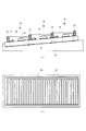
- the inside of the four-circumferential frame 34 communicates with the “L” -shaped portions of the respective slats 33. Therefore, when the sealing resin 14 is poured into the horizontally oriented wafer (package substrate 11), the sealing is performed. The resin 14 spreads uniformly on the wafer (package substrate 11) (constant depth). As shown in FIG. 8A, in the curing step, the wafer (package substrate 11) into which the sealing resin 14 has been poured is placed on a tray 35 having an inclined surface with a predetermined angle. Thereby, the sealing resin 14 is inclined relative to each package substrate 11. In this state, the sealing resin 14 is cured by oven heating or the like. Thereby, it is prevented that the thickness of the sealing resin 14 differs in each semiconductor device 10A cut out by the dicing process.
- a known dicer is used to divide the wafer in which the semiconductor devices 10A are formed in a matrix shape into a matrix by a dicing blade, and the individual semiconductor devices 10A are cut out.
- the semiconductor device 10 (10A) can be easily manufactured only by adding the groove forming step to the known manufacturing method.
- the formation of the concave groove 15 in the groove forming step can be performed together with the formation of the through hole 32, it can be easily formed by a known drilling machine or the like.
- the sealing resin 14 having an inclined surface on the surface 14a can be easily formed simply by curing the sealing resin 14 with the package substrate 11 tilted. Therefore, the semiconductor device 10 (10A) according to the embodiment having good detection sensitivity can be easily manufactured.
Landscapes
- Physics & Mathematics (AREA)
- Engineering & Computer Science (AREA)
- General Physics & Mathematics (AREA)
- Electromagnetism (AREA)
- Computer Networks & Wireless Communication (AREA)
- Radar, Positioning & Navigation (AREA)
- Remote Sensing (AREA)
- Life Sciences & Earth Sciences (AREA)
- General Life Sciences & Earth Sciences (AREA)
- Geophysics (AREA)
- Photo Coupler, Interrupter, Optical-To-Optical Conversion Devices (AREA)
Abstract
発光素子から受光素子に回り込む光のうち、パネル体等から反射して受光素子に達する光を抑制することができる半導体デバイス等を提供する。 発光素子12と受光素子13とを共通のパッケージ基板11に実装して成る半導体デバイス10であって、発光素子12および受光素子13の少なくとも一方は、パッケージ基板11に形成した逆円錐台形状の凹溝15に没するように、その溝底15aに実装され、また封止樹脂14の表面14aは、パッケージ基板11に対し、発光素子12から受光素子13に向かって下り傾斜の傾斜面で形成されている。
Description
本発明は、発光素子と受光素子とを共通のパッケージ基板に実装して成る半導体デバイス、これを備えた近接センサーおよび半導体デバイスの製造方法に関するものである。
従来、この種の半導体デバイスとして、発光素子と受光素子との間に遮光部材を配置したオプトデバイスが知られている(特許文献1参照)。このオプトデバイスは、近接する物体の有無を検知する物体検知センサーの機能を有する赤外線通信デバイスで構成されている。
オプトデバイスの物体検知センサーの部分は、基板と、基板上に搭載した発光素子および受光素子と、発光素子および受光素子を透光性樹脂で封止すると共に、発光素子に対峙する発信用レンズおよび受光素子に対峙する受信用レンズを含むモールド部と、モールド部における発信用レンズと受信用レンズとの間に形成された溝と、溝に設けられ、受光素子からの光を遮光する遮光部材と、を備えている。
発光素子から放射されてモールド部内を受光素子に向かって進む光は、溝に設けられた遮光部材により遮光される。これにより、新たにモールド金型等を必要とすることなく、モールド部内における発光素子から受光素子への光の回り込みを防止することができる。
また、ケースに収容したプリント基板を傾けた状態で、ケースに封止剤を充填する電装部品が知られている(特許文献2参照)。
オプトデバイスの物体検知センサーの部分は、基板と、基板上に搭載した発光素子および受光素子と、発光素子および受光素子を透光性樹脂で封止すると共に、発光素子に対峙する発信用レンズおよび受光素子に対峙する受信用レンズを含むモールド部と、モールド部における発信用レンズと受信用レンズとの間に形成された溝と、溝に設けられ、受光素子からの光を遮光する遮光部材と、を備えている。
発光素子から放射されてモールド部内を受光素子に向かって進む光は、溝に設けられた遮光部材により遮光される。これにより、新たにモールド金型等を必要とすることなく、モールド部内における発光素子から受光素子への光の回り込みを防止することができる。
また、ケースに収容したプリント基板を傾けた状態で、ケースに封止剤を充填する電装部品が知られている(特許文献2参照)。
ところで、このような通信機能を有するオプトデバイス(半導体デバイス)は、例えば携帯端末に搭載される。そして、携帯端末におけるオプトデバイスは、透光性のパネル体(タッチパネル)の内側に配置される場合があり、かかる場合に物体検知センサーは、パネル体越しに物体をセンシングする。
このように、従来のオプトデバイスが、パネル体に内側に配置される場合、モールド部内において発光素子から受光素子に向かう光は、遮光部材により遮光されるが、パネル体に反射して受光素子に向かう光は、遮光することができない問題があった。すなわち、発光素子から受光素子に回り込むノイズ光のうち、パネル体から反射するノイズ光を防止することができない問題があった。
このように、従来のオプトデバイスが、パネル体に内側に配置される場合、モールド部内において発光素子から受光素子に向かう光は、遮光部材により遮光されるが、パネル体に反射して受光素子に向かう光は、遮光することができない問題があった。すなわち、発光素子から受光素子に回り込むノイズ光のうち、パネル体から反射するノイズ光を防止することができない問題があった。
本発明は、発光素子から受光素子に回り込む光のうち、パネル体等から反射して受光素子に達する光を抑制することができる半導体デバイス、これを備えた近接センサーおよび半導体デバイスの製造方法を提供することを課題としている。
本発明の半導体デバイスは、共通のパッケージ基板に実装した発光素子および受光素子を、封止樹脂で封止して成る半導体デバイスであって、封止樹脂の表面は、パッケージ基板に対し、発光素子から受光素子に向かって下り傾斜の傾斜面で形成されていることを特徴とする。
この構成によれば、封止樹脂の表面が、発光素子から受光素子に向かって下り傾斜の傾斜面で形成されているため、発光素子から放射した光(検出光)は、封止樹脂の表面(空気との界面)において、全体として受光素子から離れる側に屈折する。このため、例えば前面にパネル体がある場合に、この屈折した光のうち、受光素子側においてパネル体を透過する光は、パネル体に深い角度で入射し、その反射が抑制される。すなわち、発光素子から受光素子に回り込むノイズ光のうち、パネル体から反射して受光素子に達するノイズ光を抑制することができる。なお、「パッケージ基板」は、リードフレームを含む概念である。
この場合、発光素子および受光素子は、封止樹脂のポッティングにより封止されていることが好ましい。
この構成によれば、パッケージ基板を傾斜面の角度分傾けた状態で、封止樹脂の流し込みおよび硬化を行うだけで、或いは封止樹脂の流し込みを行った後、パッケージ基板を傾けて硬化させるだけで、表面に傾斜面を有する封止樹脂を簡単に形成することができる。
また、発光素子および受光素子の少なくとも一方が、パッケージ基板に形成した凹溝に没するように実装されていることが好ましい。
この構成によれば、例えば発光素子が凹溝に実装されている場合、その放射光は、凹溝内で適宜反射し凹溝の開口部側から放射される。このため、発光素子からの放射光は、指向性を持つことになり、ノイズ光として受光素子に達することがない。しかも、凹溝により、発光素子からの放射光の取出し効率を向上させることができる。また、受光素子が凹溝に実装されている場合、受光素子に向かう発光素子からの放射光は、開口部上を通過するため、ノイズ光として受光素子に達することがない。したがって、封止樹脂内においても、発光素子から受光素子への光(ノイズ光)の回り込みを抑制することができる。
本発明の近接センサーは、上記した半導体デバイスを備え、透光性のパネル体を介して、対象物の相対的な接近をセンシングすることを特徴とする。
この構成によれば、パネル体からの反射により、受光素子に入射するノイズ光を少なくすることができる。これにより、発光素子から受光素子への光(ノイズ光)の回り込みを抑制することができ、誤検出等を有効に防止することができる。
この場合、携帯端末に搭載され、パネル体が、携帯端末のタッチパネルであることが好ましい。
この構成によれば、発光素子から受光素子への光(ノイズ光)の回り込みを抑制することができるため、人体を対象物とするセンシングを良好に行うことができる。
本発明の半導体デバイスの製造方法は、上記した半導体デバイスの製造方法であって、配線パターンを形成したパッケージ基板に、発光素子および受光素子をチップ・マウントするマウント工程と、マウント工程の後、発光素子をワイヤーボンディングすると共に、受光素子をワイヤーボンディングするボンディング工程と、ボンディング工程の後、前記パッケージ基板を水平に維持した状態で封止樹脂を流し込む工程と、前記パッケージ基板を傾けて前記封止樹脂を硬化させる工程とを経て、前記発光素子および前記受光素子を前記封止樹脂によりポッティングするポッティング工程と、を備えたことを特徴とする。
この構成によれば、水平姿勢に維持したパッケージ基板に封止樹脂を流し込み、その後、パッケージ基板を傾けて封止樹脂を硬化させるだけで、表面に傾斜面を有する封止樹脂を簡単に形成することができる。すなわち、従前の製造工程のポッティング工程において、封止樹脂を硬化させる際に、パッケージ基板を傾けるだけで、発光素子から受光素子への光(ノイズ光)の回り込みを抑制可能な半導体デバイスを簡単に製造することができる。なお、樹脂封止をウェーハレベルで実施する場合には、ポッティング工程において、デバイスの列単位でせき板(枠板)を設けるようにすることが好ましい。
この場合、ポッティング工程は、ウェーハレベルで行われ、ウェーハは、ダイシングラインの位置にそれぞれ設けたせき板と、四周縁部に設けられた四周枠とを有し、各せき板の少なくとも一方の端部は、四周枠から離間して「L」字状に屈曲していることが好ましい。
この構成によれば、封止樹脂をウェーハ全域に均一且つ円滑に流し込むことができる。また、切り離された(ダイシング)後の半導体デバイスにおける封止樹脂の厚みや傾斜角を同一にすることができる。
以下、添付の図面を参照して、本発明の一実施形態に係る半導体デバイス、これを備えた近接センサーおよび半導体デバイスの製造方法について説明する。この半導体デバイスは、発光素子と受光素子とを備えており、近接センサーとして用いられる。例えば、この近接センサーは、携帯端末(スマートフォン)に搭載され、使用者が通話中であるか否かを検出する。このため、人体から反射した微弱な反射光を確実に受光すべく、発光素子から受光素子への光の回り込みを極力防止する構成になっている。
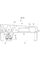
図1は、実施形態に係る半導体デバイスを、近接センサーとしてスマートフォンに搭載した場合の断面図である。同図に示すように、スマートフォン1には、その前面全域にタッチパネル2が設けられており、タッチパネル2の内側には、回路基板3に実装するようにして、レシーバー4が配設されている。また、レシーバー4に隣接して、回路基板3に実装するようにして、近接センサー5が配設されている。
すなわち、実施形態の近接センサー5は、タッチパネル2と回路基板3との間隙に配設され、タッチパネル2を介して検出光となる赤外線(実施形態のものは、近赤外線)を放射する。スマートフォン1の使用者が、通話状態に移行すべく、耳Eをレシーバー4に近づけると、近接センサー5から放射された赤外線が、耳Eの部分等で反射しその一部が、近接センサー5に入射する。近接センサー5では、入射した光(赤外線)を光―電変換し増幅して、回路基板3の判定回路(図示省略)に出力する。判定回路では、受光量(電流値)が閾値と比較され、閾値を越えることで人体(耳E)を検出、すなわち通話状態を検出する。そして、通話状態を検出したら、タッチパネル2の操作を無効とするモード切替えを実施する。
このように、実施形態の近接センサー5は、極めて近い対象物(耳E等)を検出するものであり、消費電力を抑えるべく発光量が抑えられ、且つ発光量に比して極めて少ない受光量を確実に検出する必要がある。そこで、近接センサー5を構成する本実施形態の半導体デバイス10では、S/N比を向上させるべく、ノイズ光を極力少なくなるように構成されている。
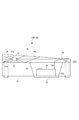
図2は、第1実施形態に係る半導体デバイス10Aの断面図である。同図に示すように、この半導体デバイス10Aは、基板フレームやリードフレーム(実施形態のものは、基板フレーム)から成るパッケージ基板11と、パッケージ基板11に実装したチップ構成の発光素子12および受光素子13と、発光素子12および受光素子13を封止する透光性の封止樹脂14と、を備えている。
受光素子13は、パッケージ基板11上に実装(マウント)される一方、発光素子12は、パッケージ基板11に形成した凹溝15に実装されている。また、封止樹脂14の表面14aは、傾斜面となっており、傾斜間隙を存してタッチパネル2(パネル体)に対峙している。
パッケージ基板11(基板フレーム)は、ガラスエポキシや有機材料の基板で構成されており、表裏両面には、発光素子12がマウントされ且つ導通される発光側配線パターン21(電極等)、および受光素子13がマウントされ且つ導通される受光側配線パターン22(電極等)が、それぞれ形成されている。また、パッケージ基板11の発光素子12が実装される部位には、逆円錐台形状の凹溝15が形成されている。そして、発光素子12は、この凹溝15の溝底15aに設けたヒートシンクを兼ねる発光側配線パターン21(ダイパッド)にマウントされている。なお、凹溝15の内周面には、反射膜を形成しておくことが好ましい。
発光素子12は、両小口端の発光面から赤外線(近赤外線)を放射する発光ダイオードのチップで構成されている。そして、発光素子12の電極パッド12aと、発光側配線パターン21のランド21aとは、ボンディングワイヤー24(金線、銅線、アルミニウム線等)で接続されている。そして、発光素子12は、パッケージ基板11に形成した凹溝15内に完全に没するように配設されている。なお、発光素子12は、上面が発光面のものであってもよい。
図2に示すように、パッケージ基板11の凹溝15内に実装された発光素子12では、その両小口端から赤外線が、凹溝12内面に反射してその開口部分から放射される。このため、検出光となる赤外線は、その放射角度が絞り込まれ(集束)指向性をもって放射されることになる。これにより、封止樹脂14の上面(空気との界面)や、タッチパネル2の下面(空気との界面)における、赤外線の反射が抑制される。すなわち、受光素子13へのノイズ光が抑制される。
受光素子13は、上面を受光面としてパッケージ基板11にマウントされたフォトダイオードのチップで構成されている。そして、受光素子13の電極パッド13aと、受光側配線パターン22のランド22aとは、ボンディングワイヤー26(金線、銅線、アルミニウム線等)で接続されている。なお、フォトダイオードに代えて、フォトトランジスタを用いてもよい。
封止樹脂14は、赤外線に対し透明なエポキシ系樹脂やシリコン系樹脂等で構成されており、発光素子12、受光素子13および各ボンディングワイヤー24,26を覆っている(封止)。この場合、封止樹脂14は、モールド成形により形成してもよいが、実施形態のものは、ポッティングにより形成されている(詳細は、後述する)。すなわち、封止樹脂14は、発光素子12や受光素子13を覆うように流し込んだ液体の封止樹脂14を、熱硬化させて形成されている。
この場合、封止樹脂14の表面14aは、パッケージ基板11に対し、発光素子12から受光素子13に向かって下り傾斜の傾斜面で形成されている。すなわち、この半導体デバイス10Aは、発光素子12側が厚手に形成され、受光素子13側が薄手に形成されている。したがって、スマートフォン1に搭載した半導体デバイス10Aは、タッチパネル2との間隙が、発光素子12側で狭く、受光素子13側が広くなるように配設されている。なお、封止樹脂14における傾斜面の角度は、封止の機能が損なわれない限りおいて、タッチパネル2との間隙幅を考慮して決定されている。
このように構成した、第1実施形態の半導体デバイス10Aでは、封止樹脂14の表面14aが、発光素子12から受光素子13に向かって下り傾斜の傾斜面で形成されているため、発光素子12から放射光は、封止樹脂14の表面(空気との界面)において、全体として受光素子13から離れる側に屈折する。このため、この屈折した光のうち、受光素子13側においてタッチパネル2を透過する光は、タッチパネル2に深い角度で入射し、その反射が抑制される。したがって、タッチパネル2からの反射によるノイズ光を抑制することができる。
また、発光素子12の放射光は、凹溝15内で適宜反射し凹溝15の開口部側から放射される。このため、発光素子12からの放射光は、絞られるようにして放射され、封止樹脂14内においてノイズ光として受光素子13に達し難くなる。したがって、発光素子12から受光素子13への光(ノイズ光)の回り込みを有効に防止することができる。しかも、凹溝15により、発光素子12からの放射光の取出し効率を向上させることができる。一方、パッケージ基板11に形成される凹溝15は、ドリルビット等で簡単に穿孔することができる。したがって、小型化および製造の容易さを維持しつつ、発光素子12から受光素子13への光(ノイズ光)の回り込みを有効に防止することができる。
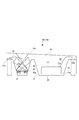
次に、図3を参照して、第2実施形態に係る半導体デバイス10Bにつき、主に第1実施形態と異なる部分について説明する。同図に示すように、この半導体デバイス10Bでは、第1実施形態と異なり、発光素子12がパッケージ基板11上に実装(マウント)される一方、受光素子13がパッケージ基板11の凹溝15に実装されている。すなわち、発光素子12は、パッケージ基板11上に形成された発光側配線パターン21にマウントされ、また受光素子13は、凹溝15に没するように、凹溝15の溝底15aに設けた受光側配線パターン22にマウントされている。
そして、この場合も、封止樹脂14の表面14aは、パッケージ基板11に対し、発光素子12から受光素子13に向かって下り傾斜の傾斜面で形成されている。また、受光素子13が凹溝15にマウントされているため、封止樹脂14の表面14aを傾斜面としても、全体として薄手に形成されている。
このように構成した、第2実施形態の半導体デバイス10Bでは、封止樹脂14の表面14aを傾斜面となっているため、受光素子13側においてタッチパネル2を透過する光は、タッチパネル2に深い角度で入射し、その反射が抑制される。したがって、タッチパネル2からの反射によるノイズ光を抑制することができる。
また、発光素子12の放射光のうちの受光素子13に向かう放射光は、凹溝15の開口部上を通過するため、封止樹脂14内においてノイズ光として受光素子13に達し難くなる。さらに、対象物(耳E)からの反射光は、凹溝15内で適宜反射し集束して受光素子13の受光面に達し、光効率良く受光される。したがって、この場合も、小型化および製造の容易さを維持しつつ、発光素子12から受光素子13への光(ノイズ光)の回り込みを有効に防止することができる。
次に、図4を参照して、第3実施形態に係る半導体デバイス10Cにつき、主に第1実施形態と異なる部分について説明する。同図に示すように、この半導体デバイス10Cでは、発光素子12および受光素子13のいずれもが、パッケージ基板11の凹溝15に実装されている。すなわち、発光素子12は、凹溝15に没するように、凹溝15の溝底15aに設けた発光側配線パターン21にマウントされ、また受光素子13は、凹溝15に没するように、凹溝15の溝底15aに設けた受光側配線パターン22にマウントされている。
そして、この場合も、封止樹脂14の表面14aは、パッケージ基板11に対し、発光素子12から受光素子13に向かって下り傾斜の傾斜面で形成されている。また、発光素子12および受光素子13が凹溝15にマウントされているため、封止樹脂14の表面14aを傾斜面としても、全体として薄手に形成されている。
このように構成した、第3実施形態の半導体デバイス10Cでは、封止樹脂14の表面14aを傾斜面となっているため、タッチパネル2からの反射によるノイズ光を抑制することができる。また、それぞれの凹溝15により、封止樹脂14内において発光素子12の放射光がノイズ光として受光素子13に達し難くなる。したがって、この場合も、小型化および製造の容易さを維持しつつ、発光素子12から受光素子13への光(ノイズ光)の回り込みを有効に防止することができる。
次に、図5を参照して、第4実施形態に係る半導体デバイス10Dにつき、主に第1実施形態と異なる部分について説明する。同図に示すように、この半導体デバイス10Dでは、従前のものと同様に、凹溝15が無く、発光素子12および受光素子13のいずれもが、パッケージ基板11上にマウントされている。そして、この場合も、封止樹脂14の表面14aは、パッケージ基板11に対し、発光素子12から受光素子13に向かって下り傾斜の傾斜面で形成されている。
このように構成した、第4実施形態の半導体デバイス10Dでは、封止樹脂14の表面14aを傾斜面となっているため、受光素子13側においてタッチパネル2を透過する光は、タッチパネル2に深い角度で入射し、その反射が抑制される。したがって、タッチパネル2からの反射によるノイズ光を抑制することができる。
次に、図2、図6、図7および図8を参照して、実施形態の半導体デバイス10(10A)の製造方法について、第1実施形態ものを例に説明する。
この製造方法は、両配線パターン21,22の形成に相前後してパッケージ基板11に、発光素子12が実装される凹溝15を形成する溝形成工程と、溝形成工程の後、パッケージ基板11に発光素子12および受光素子13をチップ・マウントするマウント工程と、マウント工程の後、発光素子12をワイヤーボンディングすると共に、受光素子13をワイヤーボンディングするボンディング工程と、ボンディング工程の後、パッケージ基板11を水平に維持した状態で封止樹脂14を流し込む工程と、パッケージ基板11を傾けて封止樹脂14を硬化させる工程とを経て、発光素子12および受光素子13を封止樹脂14によりポッティングするポッティング工程と、を備えている。
この製造方法は、両配線パターン21,22の形成に相前後してパッケージ基板11に、発光素子12が実装される凹溝15を形成する溝形成工程と、溝形成工程の後、パッケージ基板11に発光素子12および受光素子13をチップ・マウントするマウント工程と、マウント工程の後、発光素子12をワイヤーボンディングすると共に、受光素子13をワイヤーボンディングするボンディング工程と、ボンディング工程の後、パッケージ基板11を水平に維持した状態で封止樹脂14を流し込む工程と、パッケージ基板11を傾けて封止樹脂14を硬化させる工程とを経て、発光素子12および受光素子13を封止樹脂14によりポッティングするポッティング工程と、を備えている。
また、この製造方法は、樹脂封止において、いわゆるウェーハレベルパッケージとしているため、ポッティング工程において、液体の封止樹脂14をせき止めておくせき板33(詳細は、後述する)を設けるようにしている。さらに、ポッティング工程の後、ウェーハを個々の半導体デバイス10に分断するダイシング工程を備えている。
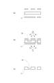
溝形成工程では、パッケージ基板11が基板フレームである場合には、表裏めっき処理された状態の基板フレームに、凹溝15を形成してもよいし、表裏めっき処理された状態の基板フレームに、配線パターンのパターン形成を行った後、凹溝15を形成してもよい。また、図6に示すように、凹溝15の形成は、専用のドリルビット31を用い、スルーホール32の形成と併せて行うことが好ましい。一方、図7に示すように、パッケージ基板11がリードフレーム(原材)である場合には、エッチング等により、凹溝15と両配線パターン21,22とを同時に形成することが好ましい。
マウント工程では、既知のダイボンディング装置を用い、発光素子12および受光素子13を銀ペースト等の接着剤を介してチップ・マウントする。
ボンディング工程では、既知のボンディング装置を用い、例えばボールボンディング方式で、発光素子12および受光素子13をワイヤーボンディングする。
ボンディング工程では、既知のボンディング装置を用い、例えばボールボンディング方式で、発光素子12および受光素子13をワイヤーボンディングする。
ポッティング工程は、ディスペンサを用い、水平姿勢のパッケージ基板11の上面全域に封止樹脂14を流し込む流込み工程と、パッケージ基板11を所定の角度傾け、封止樹脂14をオーブン加熱等により硬化させる硬化工程(図8(a)参照)と、を有している。
ポッティング工程では、ウェーハレベルでのポッティングとなるため、ウェーハには、ダイシングライン(横断方向)の位置にそれぞれせき板33が設けられ、且つ縁部には四周枠34が設けられている(図8(b)参照)。各せき板33の一方の端部は四周枠34に接続され、他方の端部は四周枠34に接続されることなく、「L」字状に屈曲している。
ポッティング工程では、ウェーハレベルでのポッティングとなるため、ウェーハには、ダイシングライン(横断方向)の位置にそれぞれせき板33が設けられ、且つ縁部には四周枠34が設けられている(図8(b)参照)。各せき板33の一方の端部は四周枠34に接続され、他方の端部は四周枠34に接続されることなく、「L」字状に屈曲している。
流込み工程では、四周枠34の内側が、各せき板33の「L」字状部分で連通しているため、水平姿勢のウェーハ(パッケージ基板11)に封止樹脂14を流し込むと、封止樹脂14は、ウェーハ(パッケージ基板11)上に均一に広がる(深さ一定)。
図8(a)に示すように、硬化工程では、封止樹脂14を流し込んだウェーハ(パッケージ基板11)を、所定角度の傾斜面を有するトレイ35に載せる。これにより、各パッケージ基板11に対し封止樹脂14が相対的に傾く。この状態で、封止樹脂14をオーブン加熱等により硬化させる。これにより、ダイシング工程により切り出された、個々の半導体デバイス10Aにおいて、封止樹脂14の厚みが異なってしまうのを防止している。
図8(a)に示すように、硬化工程では、封止樹脂14を流し込んだウェーハ(パッケージ基板11)を、所定角度の傾斜面を有するトレイ35に載せる。これにより、各パッケージ基板11に対し封止樹脂14が相対的に傾く。この状態で、封止樹脂14をオーブン加熱等により硬化させる。これにより、ダイシング工程により切り出された、個々の半導体デバイス10Aにおいて、封止樹脂14の厚みが異なってしまうのを防止している。
ダイシング工程では、既知のダイサを用い、半導体デバイス10Aをマトリクス状に作り込んだウェーハを、ダイシングブレードで縦横に分断し、個々の半導体デバイス10Aを切り出す。
このように、実施形態の半導体デバイス10(10A)の製造方法では、既知の製造方法に溝形成工程を付加しただけで、半導体デバイス10(10A)を簡単に製造することができる。しかも、溝形成工程における凹溝15の形成は、スルーホール32の形成と併せて実施することができるため、既知のドリリングマシン等で、簡単に形成することができる。また、ポッティングにおいて、封止樹脂14を、パッケージ基板11を傾けた状態で硬化させるだけで、表面14aに傾斜面を有する封止樹脂14を簡単に形成することができる。したがって、検出感度の良好な実施形態の半導体デバイス10(10A)を、簡単に製造することができる。
なお、本発明の半導体デバイスは、光デバイスとして、スマートフォン(携帯端末)の近接センサー以外の用途にも適用可能である。特に、透光性のパネル越しに設ける光デバイスとして有用である。
また、封止樹脂14の傾斜面は、湾曲面等必ずしも平面でなくてもよい(この場合には、樹脂モールドとなる。)。
また、封止樹脂14の傾斜面は、湾曲面等必ずしも平面でなくてもよい(この場合には、樹脂モールドとなる。)。
1 スマートフォン、2 タッチパネル、5 近接センサー、10,10A,10B,10C,10D 半導体デバイス、11 パッケージ基板、12 発光素子、13 受光素子、14 封止樹脂、14a 表面、15 凹溝、15a 溝底、21 発光側配線パターン、22 受光側配線パターン、24 ボンディングワイヤー、26 ボンディングワイヤー、33 せき板、34 四周枠
Claims (7)
- 共通のパッケージ基板に実装した発光素子および受光素子を、封止樹脂で封止して成る半導体デバイスであって、
前記封止樹脂の表面は、前記パッケージ基板に対し、前記発光素子から前記受光素子に向かって下り傾斜の傾斜面で形成されていることを特徴とする半導体デバイス。 - 前記発光素子および前記受光素子は、前記封止樹脂のポッティングにより封止されていることを特徴とする請求項1に記載の半導体デバイス。
- 前記発光素子および前記受光素子の少なくとも一方が、前記パッケージ基板に形成した凹溝に没するように実装されていることを特徴とする請求項1に記載の半導体デバイス。
- 請求項1に記載の半導体デバイスを備え、
透光性のパネル体を介して、対象物の相対的な接近をセンシングすることを特徴とする近接センサー。 - 携帯端末に搭載され、
前記パネル体が、前記携帯端末のタッチパネルであることを特徴とする請求項4に記載の近接センサー。 - 請求項2に記載の半導体デバイスの製造方法であって、
配線パターンを形成した前記パッケージ基板に、前記発光素子および前記受光素子をチップ・マウントするマウント工程と、
前記マウント工程の後、前記発光素子をワイヤーボンディングすると共に、前記受光素子をワイヤーボンディングするボンディング工程と、
前記ボンディング工程の後、前記パッケージ基板を水平に維持した状態で封止樹脂を流し込む工程と、前記パッケージ基板を傾けて前記封止樹脂を硬化させる工程とを経て、前記発光素子および前記受光素子を前記封止樹脂によりポッティングするポッティング工程と、を備えたことを特徴とする半導体デバイスの製造方法。 - ポッティング工程は、ウェーハレベルで行われ、
ウェーハは、ダイシングラインの位置にそれぞれ設けたせき板と、四周縁部に設けられた四周枠とを有し、
前記各せき板の少なくとも一方の端部は、前記四周枠から離間して「L」字状に屈曲していることを特徴とする請求項6に記載の半導体デバイスの製造方法。
Priority Applications (2)
| Application Number | Priority Date | Filing Date | Title |
|---|---|---|---|
| JP2014539481A JP5938479B2 (ja) | 2012-10-05 | 2012-10-05 | 半導体デバイス、これを備えた近接センサーおよび半導体デバイスの製造方法 |
| PCT/JP2012/006439 WO2014054085A1 (ja) | 2012-10-05 | 2012-10-05 | 半導体デバイス、これを備えた近接センサーおよび半導体デバイスの製造方法 |
Applications Claiming Priority (1)
| Application Number | Priority Date | Filing Date | Title |
|---|---|---|---|
| PCT/JP2012/006439 WO2014054085A1 (ja) | 2012-10-05 | 2012-10-05 | 半導体デバイス、これを備えた近接センサーおよび半導体デバイスの製造方法 |
Publications (1)
| Publication Number | Publication Date |
|---|---|
| WO2014054085A1 true WO2014054085A1 (ja) | 2014-04-10 |
Family
ID=50434447
Family Applications (1)
| Application Number | Title | Priority Date | Filing Date |
|---|---|---|---|
| PCT/JP2012/006439 Ceased WO2014054085A1 (ja) | 2012-10-05 | 2012-10-05 | 半導体デバイス、これを備えた近接センサーおよび半導体デバイスの製造方法 |
Country Status (2)
| Country | Link |
|---|---|
| JP (1) | JP5938479B2 (ja) |
| WO (1) | WO2014054085A1 (ja) |
Cited By (1)
| Publication number | Priority date | Publication date | Assignee | Title |
|---|---|---|---|---|
| KR20200001031A (ko) * | 2018-06-26 | 2020-01-06 | 삼성전자주식회사 | 발광 소자 패키지, 이를 포함하는 디스플레이 장치, 및 그 제조 방법 |
Citations (3)
| Publication number | Priority date | Publication date | Assignee | Title |
|---|---|---|---|---|
| JPH06196817A (ja) * | 1992-12-24 | 1994-07-15 | Sharp Corp | 半導体レーザ装置 |
| JP2010032254A (ja) * | 2008-07-25 | 2010-02-12 | Sharp Corp | 光半導体装置およびモバイル機器 |
| JP2010114114A (ja) * | 2008-11-04 | 2010-05-20 | Rohm Co Ltd | 反射型フォトインタラプタ |
Family Cites Families (2)
| Publication number | Priority date | Publication date | Assignee | Title |
|---|---|---|---|---|
| JP4432084B2 (ja) * | 2005-10-17 | 2010-03-17 | 株式会社山武 | レーザ計測方法、レーザ状態検知機器およびレーザ状態検知システム |
| US7495583B2 (en) * | 2006-04-14 | 2009-02-24 | Avago Technologies General Ip (Singapore) Pte. Ltd. | Flat-top reflection-based optical encoders |
-
2012
- 2012-10-05 JP JP2014539481A patent/JP5938479B2/ja active Active
- 2012-10-05 WO PCT/JP2012/006439 patent/WO2014054085A1/ja not_active Ceased
Patent Citations (3)
| Publication number | Priority date | Publication date | Assignee | Title |
|---|---|---|---|---|
| JPH06196817A (ja) * | 1992-12-24 | 1994-07-15 | Sharp Corp | 半導体レーザ装置 |
| JP2010032254A (ja) * | 2008-07-25 | 2010-02-12 | Sharp Corp | 光半導体装置およびモバイル機器 |
| JP2010114114A (ja) * | 2008-11-04 | 2010-05-20 | Rohm Co Ltd | 反射型フォトインタラプタ |
Cited By (2)
| Publication number | Priority date | Publication date | Assignee | Title |
|---|---|---|---|---|
| KR20200001031A (ko) * | 2018-06-26 | 2020-01-06 | 삼성전자주식회사 | 발광 소자 패키지, 이를 포함하는 디스플레이 장치, 및 그 제조 방법 |
| KR102530068B1 (ko) | 2018-06-26 | 2023-05-08 | 삼성전자주식회사 | 발광 소자 패키지, 이를 포함하는 디스플레이 장치, 및 그 제조 방법 |
Also Published As
| Publication number | Publication date |
|---|---|
| JPWO2014054085A1 (ja) | 2016-08-25 |
| JP5938479B2 (ja) | 2016-06-22 |
Similar Documents
| Publication | Publication Date | Title |
|---|---|---|
| US8822925B1 (en) | Proximity sensor device | |
| CN205645806U (zh) | 接近度传感器 | |
| US11513220B2 (en) | Molded proximity sensor | |
| CN108074918B (zh) | 光学式生医感测器模组及其制作方法 | |
| KR101659677B1 (ko) | 광원 일체형 광센서 및 광원 일체형 광센서의 제조방법 | |
| TW201715695A (zh) | 晶圓級光電子器件封裝及其製造方法 | |
| KR101176819B1 (ko) | 조도?근접센서 패키지 및 그 제조 방법 | |
| TWI521671B (zh) | The package structure of the optical module | |
| TW201707218A (zh) | 用以從包括多個光檢測器感測器區域的晶圓製造多個光電子元件的方法 | |
| US9134421B2 (en) | Substrate wafer with optical electronic package | |
| TW201639181A (zh) | 具有串音屏障的晶圓級光電子器件封裝及其製造方法 | |
| JP6133287B2 (ja) | 光源一体型光センサ | |
| KR20120087368A (ko) | 근접센서의 제조방법 | |
| JP2010114114A (ja) | 反射型フォトインタラプタ | |
| KR20120087779A (ko) | 근접센서의 제조방법 | |
| JP5938479B2 (ja) | 半導体デバイス、これを備えた近接センサーおよび半導体デバイスの製造方法 | |
| WO2014054083A1 (ja) | 半導体デバイス、これを備えた近接センサーおよび半導体デバイスの製造方法 | |
| WO2013168442A1 (ja) | 光源一体型光センサ、および光源一体型光センサの製造方法 | |
| JP2009010157A (ja) | オプトデバイスおよびこのオプトデバイスを搭載した電子機器 | |
| JP6104624B2 (ja) | 半導体デバイスの製造方法および半導体デバイス | |
| WO2014054082A1 (ja) | 半導体デバイス、これを備えた近接センサーおよび半導体デバイスの製造方法 | |
| WO2014054084A1 (ja) | 半導体デバイス、これを備えた近接センサーおよび半導体デバイスの製造方法 | |
| WO2016043052A1 (ja) | 光センサモジュール及びその製造方法 | |
| JP2013254930A (ja) | 光源一体型光センサ | |
| JP7257288B2 (ja) | 光センサ用パッケージ、多数個取り配線基板、光センサ装置および電子モジュール |
Legal Events
| Date | Code | Title | Description |
|---|---|---|---|
| 121 | Ep: the epo has been informed by wipo that ep was designated in this application |
Ref document number: 12886149 Country of ref document: EP Kind code of ref document: A1 |
|
| ENP | Entry into the national phase |
Ref document number: 2014539481 Country of ref document: JP Kind code of ref document: A |
|
| NENP | Non-entry into the national phase |
Ref country code: DE |
|
| 122 | Ep: pct application non-entry in european phase |
Ref document number: 12886149 Country of ref document: EP Kind code of ref document: A1 |