WO2014050586A1 - ミラー駆動装置及びその駆動方法 - Google Patents
ミラー駆動装置及びその駆動方法 Download PDFInfo
- Publication number
- WO2014050586A1 WO2014050586A1 PCT/JP2013/074648 JP2013074648W WO2014050586A1 WO 2014050586 A1 WO2014050586 A1 WO 2014050586A1 JP 2013074648 W JP2013074648 W JP 2013074648W WO 2014050586 A1 WO2014050586 A1 WO 2014050586A1
- Authority
- WO
- WIPO (PCT)
- Prior art keywords
- mirror
- piezoelectric
- piezoelectric actuator
- stress
- driving device
- Prior art date
- Legal status (The legal status is an assumption and is not a legal conclusion. Google has not performed a legal analysis and makes no representation as to the accuracy of the status listed.)
- Ceased
Links
Images

Classifications
-
- G—PHYSICS
- G02—OPTICS
- G02B—OPTICAL ELEMENTS, SYSTEMS OR APPARATUS
- G02B26/00—Optical devices or arrangements for the control of light using movable or deformable optical elements
- G02B26/08—Optical devices or arrangements for the control of light using movable or deformable optical elements for controlling the direction of light
- G02B26/0816—Optical devices or arrangements for the control of light using movable or deformable optical elements for controlling the direction of light by means of one or more reflecting elements
- G02B26/0833—Optical devices or arrangements for the control of light using movable or deformable optical elements for controlling the direction of light by means of one or more reflecting elements the reflecting element being a micromechanical device, e.g. a MEMS mirror, DMD
- G02B26/0858—Optical devices or arrangements for the control of light using movable or deformable optical elements for controlling the direction of light by means of one or more reflecting elements the reflecting element being a micromechanical device, e.g. a MEMS mirror, DMD the reflecting means being moved or deformed by piezoelectric means
-
- G—PHYSICS
- G01—MEASURING; TESTING
- G01L—MEASURING FORCE, STRESS, TORQUE, WORK, MECHANICAL POWER, MECHANICAL EFFICIENCY, OR FLUID PRESSURE
- G01L1/00—Measuring force or stress, in general
- G01L1/16—Measuring force or stress, in general using properties of piezoelectric devices
-
- G—PHYSICS
- G01—MEASURING; TESTING
- G01L—MEASURING FORCE, STRESS, TORQUE, WORK, MECHANICAL POWER, MECHANICAL EFFICIENCY, OR FLUID PRESSURE
- G01L1/00—Measuring force or stress, in general
- G01L1/16—Measuring force or stress, in general using properties of piezoelectric devices
- G01L1/162—Measuring force or stress, in general using properties of piezoelectric devices using piezoelectric resonators
-
- G—PHYSICS
- G01—MEASURING; TESTING
- G01L—MEASURING FORCE, STRESS, TORQUE, WORK, MECHANICAL POWER, MECHANICAL EFFICIENCY, OR FLUID PRESSURE
- G01L1/00—Measuring force or stress, in general
- G01L1/18—Measuring force or stress, in general using properties of piezo-resistive materials, i.e. materials of which the ohmic resistance varies according to changes in magnitude or direction of force applied to the material
-
- G—PHYSICS
- G02—OPTICS
- G02B—OPTICAL ELEMENTS, SYSTEMS OR APPARATUS
- G02B26/00—Optical devices or arrangements for the control of light using movable or deformable optical elements
- G02B26/08—Optical devices or arrangements for the control of light using movable or deformable optical elements for controlling the direction of light
- G02B26/10—Scanning systems
- G02B26/105—Scanning systems with one or more pivoting mirrors or galvano-mirrors
-
- H—ELECTRICITY
- H10—SEMICONDUCTOR DEVICES; ELECTRIC SOLID-STATE DEVICES NOT OTHERWISE PROVIDED FOR
- H10N—ELECTRIC SOLID-STATE DEVICES NOT OTHERWISE PROVIDED FOR
- H10N30/00—Piezoelectric or electrostrictive devices
- H10N30/20—Piezoelectric or electrostrictive devices with electrical input and mechanical output, e.g. functioning as actuators or vibrators
- H10N30/204—Piezoelectric or electrostrictive devices with electrical input and mechanical output, e.g. functioning as actuators or vibrators using bending displacement, e.g. unimorph, bimorph or multimorph cantilever or membrane benders
- H10N30/2041—Beam type
- H10N30/2042—Cantilevers, i.e. having one fixed end
- H10N30/2044—Cantilevers, i.e. having one fixed end having multiple segments mechanically connected in series, e.g. zig-zag type
-
- H—ELECTRICITY
- H10—SEMICONDUCTOR DEVICES; ELECTRIC SOLID-STATE DEVICES NOT OTHERWISE PROVIDED FOR
- H10N—ELECTRIC SOLID-STATE DEVICES NOT OTHERWISE PROVIDED FOR
- H10N30/00—Piezoelectric or electrostrictive devices
- H10N30/80—Constructional details
- H10N30/85—Piezoelectric or electrostrictive active materials
- H10N30/853—Ceramic compositions
- H10N30/8548—Lead-based oxides
- H10N30/8554—Lead-zirconium titanate [PZT] based
Definitions
- the present invention relates to a mirror driving device, and more particularly to a structure of a micromirror device suitable for an optical deflector used for optical scanning and a driving method thereof.
- a micro scanner (hereinafter referred to as a “MEMS (Micro Electro Mechanical System) scanner”) manufactured using silicon (Si) microfabrication technology is smaller and lower in size than a polygon mirror, which is a conventional optical scanning module. It is characterized by power consumption. For this reason, MEMS scanners are expected to have a wide range of applications, from laser projectors to optical diagnostic scanners such as optical coherence tomography (OCT).
- OCT optical coherence tomography
- a torsion bar system as shown in Patent Documents 1 and 2 is generally used.
- two or three or more torsion bars supporting the mirror are twisted to tilt the mirror and perform optical scanning.
- resonance driving is performed.
- the structure is designed so that the resonance frequency of the tilting motion of the mirror matches the driving frequency.
- Non-Patent Document 1 an angle sensor using a piezoresistive effect is provided at the base of the torsion bar
- Non- Patent Document 2 an angle sensor using a piezoelectric effect of a piezo thin film is used
- the torsion bar acting as a spring must be made extremely fragile. There is no problem.
- low frequency driving 400 Hz (hertz) or less is performed. If this is to be realized by the torsion bar method, for example, it is necessary to process Si with a thickness of 5 ⁇ m (micrometer), a width of 10 ⁇ m, and a length of 600 ⁇ m to form a torsion bar. Since this is a very fragile structure, there is a problem that it is easily destroyed when an impact is applied during the manufacturing process or during device driving. Further, an increase in the length of the torsion bar leads to an increase in the size of the element.
- Non-patent Document 3 As a design suitable for low-frequency driving, an example using a leaf spring structure (plate hinge) folded in a meander shape has been proposed (Non-patent Document 3).
- the structure shown in Non-Patent Document 3 can keep the resonance frequency low by connecting a plurality of leaf springs so as to be folded in a meander shape.
- each leaf spring has a structure with higher rigidity than that of a torsion bar, and is not easily broken by external vibration.
- Non-Patent Document 3 the conventional angle sensor shown in Non-Patent Documents 1 and 2 cannot be applied, and it is difficult to sense the angle. Therefore, a circuit that follows resonance cannot be incorporated, and it has been difficult to put it into practical use.
- the present invention has been made in view of such circumstances, and provides a mirror driving device that is small in size, can realize a large mirror tilt angle (rotation angle) at a low driving frequency, and has an angle sensing function, and a driving method thereof.
- the purpose is to do.
- a mirror driving device includes a mirror part having a reflecting surface for reflecting light, a pair of piezoelectric actuator parts arranged on both sides of the mirror part, and a rotation axis of the mirror part
- a connecting portion that connects one end of the piezoelectric actuator portion to the end portion of the mirror portion that is away from the rotating surface along the reflecting surface in a direction perpendicular to the rotation axis, and a fixing portion that supports the other end of the piezoelectric actuator portion.
- the portion has a structure including one or more plate-like members whose longitudinal direction is perpendicular to the rotation axis along the reflecting surface, and the plate-like member is bent and deformed in the thickness direction by driving the piezoelectric actuator portion.
- the connecting part has a stress detecting part for detecting the stress generated in the connecting part during the rotational driving of the mirror part due to the resonance vibration accompanied by the rotational movement of the mirror part induced by the driving of the piezoelectric actuator part. Setting It is.
- the pair of piezoelectric actuator portions are arranged so as to sandwich the mirror portion from both sides.
- One end of the piezoelectric actuator part is connected to the end part of the mirror part via the connecting part, and the other end is supported by the fixed part.
- the piezoelectric actuator unit is driven, the end of the mirror unit is displaced, and the resonance of the rotational motion is induced by the inertia torque, so that a large rotation angle (mirror tilt angle) can be obtained.
- the plate-like member of the connecting portion that functions as the plate-like hinge portion is bent (bent) in the thickness direction during the rotational drive of the mirror portion by this resonance, and the stress corresponding to this deformation is detected by the stress detection portion.
- the stress detection portion can function as an angle sensor. .
- the connecting portion has a structure in which two or more plate-like members are arranged so as to be folded back in a meander shape, and the plates arranged next to each other. It can be set as the structure which bends and deform
- each plate-like hinge portion composed of a plurality of plate-like members connected in a meander shape, it is easy to design to keep the resonance frequency low. Further, since each plate-like member can have a structure with relatively high rigidity, it becomes a structure that is not easily destroyed by external vibration.
- two or more plate-like members arranged so as to be folded back in a meander shape are arranged in the direction from the side close to the mirror portion toward the piezoelectric actuator portion.
- a first stress detection unit that detects a stress generated in an odd-numbered plate-shaped member and an even-numbered plate-shaped member as a stress detection unit when specifying each plate-shaped member by giving a sequential number indicating the order
- a second stress detection unit for detecting the stress generated in the.
- the stress detection unit is a laminate in which a lower electrode, a piezoelectric body, and an upper electrode are sequentially laminated on a plate-like member. It has a structure, and it can be set as the structure which converts stress into an electric signal by the piezoelectric effect of a piezoelectric material.
- the stress applied to the plate-like member can be detected as a voltage between the upper electrode and the lower electrode, and can function as an angle sensor.
- the detection sensitivity can be improved and the signal / noise ratio (S / N ratio) can be improved.
- the stress detection unit is formed of a material in which a surface portion of the plate-like member exhibits a piezoresistance effect, and the piezoresistance It can be set as the structure which converts stress into the change of resistance value by the piezoresistive effect of the material which shows an effect.
- the means for detecting the stress applied to the connecting portion is not limited to the configuration using the piezoelectric effect, and a configuration using the piezoresistance effect can be employed.
- the mirror driving device may include a detection circuit that converts a change in resistance value into a voltage signal.
- the detection circuit is configured by a first resistor and a second stress detection unit configured by the first stress detection unit.
- the voltage signal can be obtained by a voltage dividing circuit connected to the second resistor.
- the piezoelectric actuator unit includes a piezoelectric unimorph cantilever in which a diaphragm, a lower electrode, a piezoelectric body, and an upper electrode are stacked in this order. It can consist of.
- the piezoelectric cantilever is not limited to a unimorph structure but can also be a bimorph structure, but the unimorph structure is the simplest configuration. Since the piezoelectric drive system can be driven simply by applying a voltage between the electrodes, the structure is simple and it is beneficial for miniaturization.
- the piezoelectric body used in the piezoelectric actuator section and the stress detection section is a thin film having a thickness of 1 to 10 ⁇ m, It can be a thin film directly formed on the substrate.
- the piezoelectric actuator part and the stress detection part can be manufactured by the same process.
- a piezoelectric thin film having a required piezoelectric performance can be obtained by using a direct film formation method such as a vapor phase growth method represented by a sputtering method or a sol-gel method.
- a direct film formation method such as a vapor phase growth method represented by a sputtering method or a sol-gel method.
- the piezoelectric body used in the piezoelectric actuator unit is one or two kinds represented by the following formula (P):
- the above perovskite oxide can be obtained.
- General formula ABO 3 (P) (In the formula, A: an element of A site, and at least one element including Pb.
- O Oxygen element.
- the molar ratio of the A site element, the B site element, and the oxygen element is 1: 1: 3 as a standard, but these molar ratios may deviate from the reference molar ratio within a range where a perovskite structure can be taken. ) Note that the same piezoelectric material as that of the piezoelectric actuator unit can be used for the piezoelectric body used in the stress detection unit.
- the piezoelectric body used in the piezoelectric actuator unit is one or two kinds represented by the following formula (PX)
- PX The above perovskite oxide can be obtained.
- A (Zr x , Ti y , M bxy ) b O c (PX)
- A an element of A site, and at least one element including Pb.
- M At least one element selected from the group consisting of V, Nb, Ta, and Sb. 0 ⁇ x ⁇ b, 0 ⁇ y ⁇ b, 0 ⁇ b ⁇ xy.
- PZT doped with an element such as Nb has a high piezoelectric constant, it is suitable for manufacturing a small device capable of obtaining a large displacement. Note that the same piezoelectric material as that of the piezoelectric actuator unit can be used for the piezoelectric body used in the stress detection unit.
- the perovskite oxide (PX) contains Nb, and the Nb / (Zr + Ti + Nb) molar ratio is 0.06 or more and 0.20 or less. It is preferable to do.
- Such a material exhibits good piezoelectric properties without performing polarization treatment. Therefore, the polarization process is unnecessary, and the manufacturing process can be simplified and the cost can be reduced.
- the piezoelectric body used in the piezoelectric actuator portion can be a thin film formed by sputtering.
- the driving circuit for supplying a driving voltage for resonantly driving the mirror unit in the vicinity of the resonance frequency fx of the resonance mode in which the rotary motion is performed can be provided.
- a mirror driving method in the mirror driving device according to any one of the first to fifteenth aspects, wherein a driving voltage is applied to a pair of piezoelectric actuator parts to vibrate the piezoelectric actuator parts.
- a mirror driving method including vibrating the connecting portion between the mirror portion and the coupling portion, applying a rotational torque around the rotation axis to the mirror portion by the vibration, and driving the mirror portion to resonate.
- the driving voltage or the driving frequency applied to the piezoelectric actuator unit is controlled using a detection signal obtained from the stress detecting unit during the resonance driving of the mirror unit. Can further be included.
- At least one of the frequency (drive frequency) and amplitude of the drive voltage supplied to the piezoelectric actuator unit can be controlled based on the detection signal obtained from the stress detection unit.
- a stable resonance drive can be realized by feeding back a detection signal obtained from the stress detection unit to the drive of the piezoelectric actuator unit.
- a mirror driving device that is smaller than a conventional torsion bar system, can realize a large mirror tilt angle (rotation angle) with a low driving frequency, and is equipped with an angle sensing function.
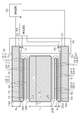
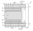
- FIG. 1 is a perspective view of the MEMS scanner device according to the first embodiment.
- FIG. 2 is an explanatory diagram combining a plan view of the MEMS scanner device of FIG. 1 viewed from the reflection surface side of the mirror portion and a block configuration diagram showing circuit elements.
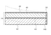
- FIG. 3 is a cross-sectional view of the piezoelectric actuator portion.
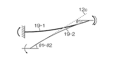
- FIG. 4 is a perspective view showing a state during driving in the rotational resonance mode.
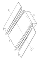
- FIG. 5 is a schematic view of the first connecting portion (plate hinge) shown in FIG. 4 as viewed from the positive direction of the y-axis.
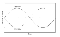
- FIG. 6 is a diagram illustrating an example of an angle detection signal obtained by detecting the stress of the connecting portion.
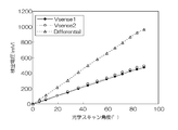
- FIG. 7 is a graph showing the relationship between the optical scan angle and the detection voltage.
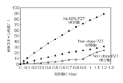
- FIG. 8 is a graph showing the relationship between the applied voltage and the optical scan angle.
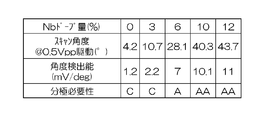
- FIG. 9 is a chart summarizing the relationship between the Nb doping amount in PZT and the actuator characteristics / sensing characteristics.
- FIG. 10 is a plan view showing the configuration of the MEMS scanner device according to the second embodiment.
- FIG. 11 is a diagram illustrating a configuration example of a detection circuit applied to the second embodiment.
- FIG. 12 is a plan view showing the configuration of the MEMS scanner device according to the third embodiment.
- FIG. 13 is a perspective view showing a state during driving in the rotational resonance mode in the third embodiment.
- FIG. 1 is a perspective view of the MEMS scanner device according to the first embodiment.
- FIG. 2 is a combination of a plan view (top view) of the MEM scanner device according to the first embodiment viewed from the reflection surface side of the mirror unit and a block configuration diagram showing circuit elements for device driving and angle detection.
- the MEMS scanner device 10 (corresponding to a “mirror drive device”) of this example includes a mirror unit 12 and a pair of piezoelectric actuator units 14 disposed on both sides of the mirror unit 12. , 16, connecting portions 18, 20 that connect one end portion 14 ⁇ / b> A, 16 ⁇ / b> A of each piezoelectric actuator portion 14, 16 and the end portions 12 ⁇ / b> A, 12 ⁇ / b> B of the mirror portion 12, and the other end portion of the piezoelectric actuator portions 14, 16. (Hereinafter, referred to as a base end portion) 14B and 16B.
- the piezoelectric actuator part 14 may be referred to as a “first piezoelectric actuator part”, and the piezoelectric actuator part 16 may be referred to as a “second piezoelectric actuator part”.
- the connection part 18 is referred to as a “first connection part”
- the connection part 20 is referred to as a “second connection part”
- the end part 12 ⁇ / b> A is referred to as a “first end part”
- the end part 12 ⁇ / b> B is referred to as an end part.
- second end Sometimes referred to as “second end”.
- the mirror part 12 of this example is substantially rectangular in a plan view as shown in the figure, and the mirror surface (the upper surface of the mirror part 12) that becomes the reflection surface 12C that reflects light is used to increase the reflectance of incident light.
- a metal thin film such as Au (gold) or Al (aluminum) is formed.
- the material and film thickness used for the mirror coating are not particularly limited, and various designs are possible using a known mirror material (high reflectivity material).
- rectangular is not limited to a strict rectangular shape (rectangular shape), but means a shape that can be generally grasped as a rectangular shape as an overall basic shape.
- a rectangular corner portion is chamfered, a corner portion is rounded, a part or all of a side is formed by a curve or a broken line, a connecting portion between the mirror portion 12 and each of the connecting portions 18 and 20
- additional shapes necessary for connection are added.
- the shape of the mirror portion 12 is not particularly limited. Not only the rectangle illustrated in FIGS. 1 and 2 but also various shapes such as a square, a polygon, a circle, and an ellipse can be used. Further, the planar view shape of the mirror part 12 and the shape of the reflection surface 12C may be the same or different.
- the reflection surface 12 ⁇ / b> C can be formed within the area of the upper surface of the mirror portion 12.
- the mirror part 12 having a substantially rectangular reflecting surface 12C in plan view is illustrated, the long side direction of the mirror part 12 when not driven is in the x direction, the short side direction orthogonal to this is the y direction, and the xy plane An orthogonal xyz axis with the direction perpendicular to z as the z direction will be described.
- the MEMS scanner device 10 has a pair of piezoelectric actuator portions 14 and 16 disposed so that the mirror portion 12 with the reflecting surface 12C facing in the z-axis direction is sandwiched from both sides in the y-axis direction when not driven.
- Each of the piezoelectric actuator units 14 and 16 is an actuator having a piezoelectric unimorph cantilever (cantilever) structure (see FIG. 3), and performs bending displacement by deformation of the piezoelectric body due to the inverse piezoelectric effect. That is, the piezoelectric actuator portions 14 and 16 are fixedly supported by the fixed frame 30 at one end in the x direction (base ends 14B and 16B), and the opposite end portions 14A and 16A are not fixed to the frame or the like. It is an unconstrained end that can be displaced by the cantilever structure.
- the end portion 14A on the non-constraining side of the first piezoelectric actuator portion 14 is connected to one end portion 18A of the first connecting portion 18 configured in a meander shape.
- the other end portion 18B of the first connecting portion 18 is connected to the first end portion 12A on the side of the mirror portion 12 along the x-axis direction.
- the non-constrained end 16A of the second piezoelectric actuator section 16 is connected to one end 20A of the second connecting section 20 configured in a meander shape.
- the other end 20B of the second connecting portion 20 is connected to the second end 12B in the x-axis direction of the mirror portion 12.
- the end portions (12A, 12B) in the x-axis direction of the mirror portion 12 to which the first connecting portion 18 and the second connecting portion 20 are respectively connected are not required to be the extreme end positions in a strict sense, and generally It includes a part of a range (the extreme end position and the vicinity thereof) that can be grasped as an end part.
- the MEMS scanner device 10 of this example drives the first piezoelectric actuator unit 14 and the second piezoelectric actuator unit 16 to move the end portions (12A, 12B) of the mirror unit 12 up and down (in the thickness direction of the mirror unit 12).
- the mirror unit 12 is excited to rotate and revolve around the rotation axis 22 parallel to the y-axis, thereby driving the mirror unit 12 to rotate (see FIG. 4).
- the rotation axis 22 is a straight line that passes through substantially the center point of the reflecting surface 12C and is parallel to the y-axis.
- the first connecting portion 18 and the second connecting portion 20 are connected to a portion in the vicinity of the end portion of the mirror portion 12 that is separated from the mirror center in the x-axis direction within a range in which such a target resonance drive can be achieved. That is, the first end portion 12A and the second end portion 12B of the mirror portion 12 to which the first connecting portion 18 and the second connecting portion 20 are connected are in the x-axis direction (rotating axis) from the rotating shaft 22 along the reflecting surface 12C. This is a portion including the range of the vicinity of the end of the mirror portion 12 and the vicinity of the end of the mirror portion 12 that is separated in a direction perpendicular to the uppermost portion 22.
- the first connecting portion 18 and the second connecting portion 20 have a structure in which a plurality of flat plate-like thin plate members 19 (corresponding to “plate-like members”) whose longitudinal direction is the x-axis direction are arranged in a meander shape.
- a structure in which two thin plate members 19 are arranged in parallel and end portions of these two thin plate members 19 are connected so as to be folded back in a meander shape is not particularly limited, and may be one or more and an appropriate number.
- the first connecting portion 18 and the second connecting portion 20 drive the first piezoelectric actuator portion 14 and the second piezoelectric actuator portion 16, respectively, so that each thin plate member 19 is bent (bent) and deformed in the thickness direction. Function as.
- the mirror portion 12 is subjected to acceleration directions (force is applied to the end portions 14A and 16A of the piezoelectric actuator portions 14 and 16). Inertia force in the opposite direction works. Since this inertial force coincides with the direction in which the mirror unit 12 is tilted, the force generated by the piezoelectric actuator units 14 and 16 is efficiently used as the force for tilting the mirror unit 12.
- each of the connecting units 18 and 20 is associated with the displacement of the piezoelectric actuator units 14 and 16.
- the thin plate member 19 bends (bends), and inertia torque is generated in the mirror portion 12 to induce rotational motion resonance of the mirror portion 12.
- the displacement direction of the piezoelectric actuator parts 14 and 16 always coincides with the rotation direction of the mirror part 12 and all the force is used for rotation of the mirror, the use efficiency of the force is much better than that of the torsion bar structure, Even if the rotation angle increases, a large displacement (inclination angle) can be obtained because there is little energy loss.
- each thin plate member 19 bends little by little and accumulates displacement, so that the stress applied to each thin plate member 19 is increased. There is an advantage that it is less likely to be destroyed even when the rotation angle is high.
- the plurality of thin plate members 19 constituting the first connecting portion 18 and the second connecting portion 20 are sequentially directed from the left in FIG. 1 toward the right (from the top to the bottom in FIG. 2). ), The first thin plate member 19-1, the second thin plate member 19-2, the third thin plate member 19-3, and the fourth thin plate member 19-4.
- the first connecting portion 18 is configured by connecting the first thin plate member 19-1 and the second thin plate member 19-2.
- the second connecting portion 20 is configured by connecting a third thin plate member 19-3 and a fourth thin plate member 19-4.
- Numerals 31, 32, 33, and 34 provided on the surface of the fixed frame 30 in the drawing are output terminals for detection signal output.
- Each wiring 51 to 54 is patterned on the piezoelectric film.
- the wiring 51 drawn from the detection electrode 25-1 formed on the upper surface of the first thin plate member 19-1 is located alongside the upper electrode (drive electrode 15) of the first piezoelectric actuator section 14 from the first thin plate member 19-1. Is routed along the longitudinal direction and connected to the output terminal (first output terminal) indicated by reference numeral 31.
- the wiring 52 drawn from the detection electrode 25-2 formed on the upper surface of the second thin plate member 19-2 is routed along the longitudinal direction alongside the detection electrode 25-1 of the first thin plate member 19-1.
- the side of the upper electrode (drive electrode 15) of the first piezoelectric actuator unit 14 is routed along the longitudinal direction and connected to the output terminal (second output terminal) indicated by reference numeral 32.
- the wiring 53 drawn from the detection electrode 25-3 formed on the upper surface of the third thin plate member 19-3 is routed along the longitudinal direction alongside the detection electrode 25-4 of the fourth thin plate member 19-4. At the same time, it is routed along the longitudinal direction along the upper electrode (drive electrode 17) of the second piezoelectric actuator section 16, and is connected to an output terminal (third output terminal) indicated by reference numeral 33.
- the wiring 54 drawn from the detection electrode 25-4 formed on the fourth thin plate member 19-4 is located beside the upper electrode (drive electrode 17) of the second piezoelectric actuator section 16 from the fourth thin plate member 19-4. Is routed along the longitudinal direction and connected to an output terminal (fourth output terminal) indicated by reference numeral 34.
- the first piezoelectric actuator unit 14 and the second piezoelectric actuator unit 16 are connected to the drive circuit 62 via a wiring member such as wire bonding.
- FIG. 3 is a schematic diagram showing a cross-sectional structure of the piezoelectric actuator portions 14 and 16 having a piezoelectric unimorph cantilever structure. Since the piezoelectric actuator portions 14 and 16 have the same structure, the structure of the piezoelectric actuator portion denoted by reference numeral 14 will be described as a representative. In implementing the present invention, a structure other than a unimorph cantilever may be used as the piezoelectric actuator portion. For example, you may use the bimorph cantilever which laminated
- the piezoelectric actuator unit 14 has a structure in which a lower electrode 43, a piezoelectric body 46, and an upper electrode 48 are stacked on a vibration plate 42.
- a laminated structure can be obtained, for example, by sequentially depositing the lower electrode 43, the piezoelectric body 46, and the upper electrode 48 on a silicon (Si) substrate.
- the right end in FIG. 3 is a fixed end supported by a fixed frame 30 (see FIGS. 1 and 2).
- the piezoelectric body 46 is deformed by applying a drive voltage between the electrodes (43, 48), and the diaphragm 42 is bent along with this deformation, and the lever portion moves up and down.
- a broken line in FIG. 3 represents a state in which the lever portion is displaced upward.
- the piezoelectric actuator units 14 and 16 are means for converting an electrical signal into a mechanical displacement using the inverse piezoelectric effect of the piezoelectric body 46.
- the same drive voltage is simultaneously applied to the pair of piezoelectric actuator units 14 and 16 from the drive circuit 62 to displace the piezoelectric actuator units 14 and 16 on both sides of the mirror unit 12 in the same direction.
- a common (same) drive circuit 62 can be used as a power supply source for supplying drive power to the pair of piezoelectric actuator units 14 and 16.
- a sine waveform signal or a pulse waveform signal having a frequency for exciting resonance can be used as a sine waveform signal or a pulse waveform signal having a frequency for exciting resonance.
- the MEMS scanner device 10 operates as follows.
- the piezoelectric actuator units 14 and 16 are vibrated up and down to induce a rotational motion in the mirror unit 12.
- the mirror unit 12 vibrates with a large tilt angle by applying a drive voltage having a frequency near the resonance frequency to drive resonance.
- the meander-like connecting portions 18 and 20 are easily bent and deformed, it is effective to obtain a large displacement in resonance driving (see FIGS. 4 and 5).
- the frequency of the drive voltage applied to the piezoelectric actuator sections 14 and 16 is not necessarily required to exactly match the mechanical resonance frequency of the structure. A difference in the frequency of the drive voltage is allowed in a range where resonance is excited.
- the mirror part 12 can be displaced with a large rotation angle around the rotation axis 22 by this rotational resonance drive. That is, according to the driving of the piezoelectric actuator units 14 and 16, the central mirror unit 12 is swung around the rotation shaft 22. Light incident on the reflecting surface 12C of the mirror unit 12 (for example, laser light emitted from a laser light source (not shown)) is reflected according to the inclination (angle) of the mirror unit 12, and the traveling direction of the reflected light (the reflected light) (Irradiation position) changes. According to the MEMS scanner device 10 according to the present embodiment, optical scanning can be performed with a large deflection angle.
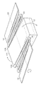
- FIG. 4 and 5 are explanatory diagrams for explaining the stress ( ⁇ xx component) related to the connecting portion (plate hinge portion) during resonance driving.
- FIG. 4 is a perspective view showing a state during driving in the rotational resonance mode
- FIG. 5 is a schematic view of the first connecting portion 18 shown in FIG. 4 viewed from the positive direction of the y-axis.
- the illustration of the fixed frame 30 is omitted.
- the movement of the second connecting portion 20 is the same as the movement of the first connecting portion 18 due to the symmetry of the device structure.
- the thin plate members 19-1 and 19-2 constituting the first connecting portion 18 are bent and deformed in opposite directions to each other, and the respective thin plate members 19-1, 19- Stress acts on the surface of 2 in opposite directions. That is, as shown in FIG. 5, when the first thin plate member 19-1 moves downward (curvature deformation), the second thin plate member 19-2 moves upward. At this time, compressive stress is applied to the surface of the first thin plate member 19-1, and tensile stress is applied to the surface of the second thin plate member 19-2.
- first thin plate member 19-1 (hinge 1) and second thin plate member 19-2 (hinge 2) bend in the opposite directions, and the angular displacement ⁇ 1 due to the bending of the first thin plate member 19-1.
- the angle displacement ⁇ 2 due to the bending of the second thin plate member 19-2 is added to obtain the tilt angle of the mirror portion 12.
- the reflecting surface 12C of the mirror unit 12 is inclined at an angle of ( ⁇ 1 + ⁇ 2) around the y axis.
- the stress on the first thin plate member 19-1 and the second thin plate member 19-2 is detected as the voltage between the upper and lower electrodes of the sensor units 24-1 and 24-2 by the piezoelectric effect, and the angle It functions as a sensor.
- an AGC Automatic Gain Control
- PLL phase-locked loop
- Such a feedback control circuit can be incorporated in the detection circuit 64.
- the drive circuit 62, the detection circuit 64, and the feedback control circuit can be collectively configured by an integrated circuit such as an ASIC (Application Specific Specific Integrated Circuit).
- a sensor portion may be provided in a part of the thin plate member 19, and a detection electrode having an appropriate size can be designed.
- the area of the detection electrode of the sensor unit is relatively small from the viewpoint of relatively reducing the influence of the parasitic capacitance component / resistance component of the subsequent stage such as the wiring unit A relatively large size is desirable.
- Examples of the piezoelectric body suitable for the present embodiment include those containing one or more perovskite oxides (P) represented by the following formula.
- ABO 3 (P) (In the formula, A: an element of A site, and at least one element including Pb.
- O Oxygen element.
- the molar ratio of the A site element, the B site element, and the oxygen element is 1: 1: 3 as a standard, but these molar ratios may deviate from the reference molar ratio within a range where a perovskite structure can be taken.
- Perovskite oxides represented by the above general formula include lead titanate, lead zirconate titanate (PZT), lead zirconate, lead lanthanum titanate, lead lanthanum zirconate titanate, lead zirconium titanate niobate , Lead-containing compounds such as lead zirconium niobate titanate titanate and lead zinc niobate titanate titanate, and mixed crystals thereof; barium titanate, strontium barium titanate, bismuth sodium titanate, bismuth potassium titanate, niobic acid Non-lead-containing compounds such as sodium, potassium niobate, lithium niobate, bismuth ferrite, and mixed crystals thereof can be mentioned.
- PZT lead zirconate titanate
- lead lanthanum titanate lead lanthanum zirconate titanate
- lead zirconium titanate niobate Lead-containing compounds such as lead zirconium niobate titan
- the piezoelectric film of the present embodiment preferably includes one or more perovskite oxides (PX) represented by the following formula.
- A (Zr x , Ti y , M b-xy ) b O c (PX)
- A an element of A site, and at least one element including Pb.
- M is at least one element selected from the group consisting of V, Nb, Ta, and Sb. 0 ⁇ x ⁇ b, 0 ⁇ y ⁇ b, 0 ⁇ b ⁇ xy.
- the perovskite oxide (PX) is an intrinsic PZT or a part of the B site of PZT substituted with M. It is known that PZT to which various donor ions having a valence higher than that of the substituted ion are added has improved characteristics such as piezoelectric performance as compared with intrinsic PZT.
- M is preferably one or more donor ions having a valence higher than that of tetravalent Zr or Ti. Examples of such donor ions include V 5+ , Nb 5+ , Ta 5+ , Sb 5+ , Mo 6+ , and W 6+ .
- Bxy is not particularly limited as long as it has a perovskite structure.
- M is Nb
- the Nb / (Zr + Ti + Nb) molar ratio is preferably 0.05 or more and 0.25 or less, and more preferably 0.06 or more and 0.20 or less.
- the piezoelectric film made of the perovskite oxide represented by the above general formulas (P) and (PX) has a high piezoelectric strain constant (d31 constant), the piezoelectric actuator provided with such a piezoelectric film is displaced. Excellent characteristics.
- the piezoelectric actuator provided with the piezoelectric film made of the perovskite oxide represented by the general formulas (P) and (PX) has voltage-displacement characteristics with excellent linearity. These piezoelectric materials exhibit good actuator characteristics and sensor characteristics in practicing the present invention. Note that the perovskite oxide represented by the general formula (PX) has a higher piezoelectric constant than that represented by the general formula (P).
- a lead zirconate titanate (PZT) thin film doped with 12% of Nb in atomic composition percentage can be used.
- a bulk piezoelectric body may be bonded to the substrate and polished.
- the piezoelectric body 46 of the present embodiment is preferably a thin film having a thickness of 1 ⁇ m or more and 10 ⁇ m or less.
- Vapor phase epitaxy is preferred as the piezoelectric film formation method.
- various methods such as ion plating, MOCVD (metal organic chemical vapor deposition), and PLD (pulse laser deposition) can be applied in addition to sputtering. It is also conceivable to use a method other than the vapor phase growth method (for example, a sol-gel method).
- Example 1 which will be described later, a PZT thin film having a thickness of 4 ⁇ m formed by sputtering is used as the piezoelectric body 46, but is not limited thereto.
- Example 1 an example of a specific manufacturing method> As Example 1, a MEMS scanner device 10 was manufactured by the following procedure.
- Step 1 On a SOI (Silicon On Insulator) substrate having a handle layer of 350 ⁇ m, a box layer of 1 ⁇ m, and a device layer of 10 ⁇ m, a Ti layer of 30 nm and an Ir electrode layer of 150 nm were formed by a sputtering method at a substrate temperature of 350 ° C. These Ti layer and Ir electrode layer correspond to the lower electrode 43 in FIG.
- SOI Silicon On Insulator
- Step 2 A PZT layer having a thickness of 4 ⁇ m was formed on the obtained substrate using a radio frequency (RF) sputtering apparatus.
- a film forming gas was a mixed gas of 97.5% Ar and 2.5% O 2 , and a target material having a composition of Pb 1.3 ((Zr 0.52 Ti 0.48 ) 0.88 Nb 0.12 ) O 3 was used.
- the film forming pressure was 2.2 mTorr (about 0.293 Pa), and the film forming temperature was 450 ° C.
- the obtained PZT layer was an Nb-doped PZT thin film in which Nb was added at 12% by atomic composition ratio.
- Step 3 A Pt / Ti layer as an upper electrode was patterned on the substrate obtained above by lift-off, and the PZT thin film was pattern etched by ICP (inductively coupled plasma) dry etching.
- ICP inductively coupled plasma
- Step 4 the device layer was pattern-etched by a silicon dry etch process, and the handle layer was deep-etched (Deep RIE; Reactive Ion Etching) from the back surface. Finally, by removing the Box-SiO 2 layer from the back surface, a piezoelectric MEMS scanner device configured as shown in FIG. 1 was produced.
- the fixed frame 30 has a structure using both the handle layer and the device layer, and has a thickness of about 360 ⁇ m.
- Both the piezoelectric actuator part and the plate-like hinge part have a laminated structure of Si device layer (10 ⁇ m) / lower electrode / PZT thin film / upper electrode.
- the piezoelectric actuator unit functions as a piezoelectric thin film unimorph actuator that bends up and down when a voltage is applied between the upper and lower electrodes.
- Piezoelectric actuators 14 and 16 have a laminated structure of Si device layer (10 ⁇ m) / lower electrode / PZT thin film / upper electrode and function as a piezoelectric thin film unimorph actuator.
- Example 1 a PZT thin film is formed directly on a substrate by a sputtering method, and then dry-etched.
- the creation process can be simplified and fine patterning can be performed.
- the yield can be significantly improved and further miniaturization of the device can be accommodated.
- the configuration for implementing the present invention is not limited to a thin film piezoelectric body, but a unimorph actuator is formed by pasting a bulk piezoelectric body to a diaphragm, or a bimorph actuator by pasting two piezoelectric bodies having different polarities. It is also good.
- the substrate material, the electrode material, the piezoelectric material, the film thickness, the film forming conditions, and the like can be appropriately selected according to the purpose without being limited to the first embodiment.
- Example 1 ⁇ Evaluation of MEMS Scanner Device According to Example 1>
- a rotational resonance motion around the rotation axis of the mirror was induced, and the mechanical shake angle of the mirror portion was measured by the laser scan angle.
- the resonance frequency fx was 154 Hz and the mechanical shake angle was ⁇ 22 °.
- a voltage output with a potential amplitude of 470 mV (millivolts) was obtained from 25-1 and 25-4, a voltage output with a potential amplitude of 490 mV was obtained from the detection electrodes 25-2 and 25-3, and the phase difference between these signals was 180 °. (See FIG. 7).
- Vsense1 indicates signals from the detection electrodes 25-1 and 25-4
- Vsense2 indicates signals from the detection electrodes 25-2 and 25-3.
- FIG. 7 shows a plot of the relationship between the scan angle and the detection voltage by changing the drive voltage applied to the piezoelectric actuator sections 14 and 16.
- “Differential” indicates that the difference between the two voltage signals (Vsense1, Vsense2) is detected by the difference circuit.
- the angle detection ability of each detection electrode was as follows.
- Vsense1 5.41 mV / deg
- Vsense2 5.61 mV / deg Difference: 11 mV / deg
- the MEMS scanner device 10 shown in FIG. 1 has a symmetrical structure with the mirror portion 12 interposed therebetween, and the first thin plate member 19-1 and the fourth thin plate member 19-2 are at resonance drive. Are equivalent movements, and the second thin plate member 19-2 and the third thin plate member 19-3 are equivalent movements.
- the same detection signal (Vsense1 in FIG. 6) is obtained from the sensor unit 24-1 on the first thin plate member 19-1 and the sensor unit 24-4 on the fourth thin plate member 19-4.
- a similar detection signal (Vsense2 in FIG. 6) is obtained from the sensor portion 24-2 on the second thin plate member 19-2 and the sensor portion 24-3 on the third thin plate member 19-3.
- a combination of the third thin plate member 19-3, a combination of the second thin plate member 19-2 and the fourth thin plate member 19-4, and a combination of the third thin plate member 19-3 and the fourth thin plate member 19-4 are also possible. Any combination may be adopted.
- the number of thin plate members constituting the meander-like connecting portions (18, 20) is generalized as m (m is an integer of 2 or more), the m thin plate members are outward from the side closer to the mirror portion 12.
- the initial value of the serial number j is not limited to “1”, and may be “0”, and may be an arbitrary integer.
- a sensor unit that detects a stress generated in at least one thin plate member selected from among the odd-numbered thin plate members, and a stress generated in at least one thin plate member selected from among the even-numbered thin plate members. What is necessary is just to detect a signal from both of these sensor parts as a structure provided with a sensor part.
- Example 2 In Example 2, the same production method as in Example 1 was used except that a target material at the time of PZT film formation was Pb 1.3 ((Zr 0.52 Ti 0.48 ) O 3 ). The MEMS scanner device having the structure was manufactured, and an operation confirmation experiment was performed on the obtained device in the same manner as in Example 1. Fig. 8 shows the relationship between the applied voltage and the optical scan angle. The results of Example 1 (Nb12% PZT) are also shown.
- the white triangles in FIG. 8 are the results of measurement without performing polarization treatment on PZT not doped with Nb.
- the black triangles are the measurement results when PZT not doped with Nb is polarized after film formation.
- the black circles are the measurement results of Example 1 using PZT doped with 12% Nb (no polarization treatment).
- FIG. 9 shows a table summarizing the relationship between the Nb doping amount in PZT and the actuator characteristics / sensing characteristics.
- unpolarized values are used for both the scan angle and the angle detection capability.
- the determination regarding the necessity of the polarization process is “C” (the polarization process is necessary) when the scan angle in the unpolarized state (when 0.5 Vpp is applied) is 0.8 or less of the scan angle after the polarization process. , 0.8 and 0.9 or less, “A” (can be used in unpolarized treatment), and 0.9 above “AA” (no polarization treatment required).
- the PZT can be used without performing polarization treatment by doping Nb with 6% or more, the manufacturing cost can be reduced.
- the higher the Nb doping amount the higher the scan angle can be obtained at a lower voltage, and the higher detection voltage can be obtained during angle detection.
- the stress applied to the connecting portions 18 and 20 during the rotational motion is detected as a voltage signal by the piezoelectric effect.
- the angle of the mirror part 12 can be grasped from this voltage signal.
- a MEMS scanner device can be formed by directly forming a PZT thin film on a substrate and etching it. As described above, since the fine patterning can be easily performed by thinning the piezoelectric body, the yield can be greatly improved and the device can be further miniaturized.
- a structure in which a piezoelectric thin film is laminated on the connecting portions 18 and 20 functioning as a plate-like hinge portion and stress is converted into a voltage by the piezoelectric effect is used.
- the means for detecting the stress is not limited to this example.
- a form using the piezoresistive effect as means for detecting the stress generated in the connecting portion is also possible.
- boron (boron) doping is performed on the surfaces of the connecting portions 18 and 20 of silicon (Si) to form a p-type Si layer exhibiting a piezoresistive effect, and the electric resistance of the p-type Si layer depends on the applied stress. You may employ
- FIG. 10 is a plan view showing the configuration of the MEMS scanner device according to the second embodiment. 10, elements that are the same as or similar to those in FIGS. 1 and 2 are given the same reference numerals, and descriptions thereof are omitted.
- the stress is detected using.
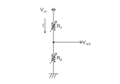
- FIG. 11 is a configuration diagram of a circuit that converts a change in resistance value into a voltage.
- R1 and R2 in the figure indicate the resistances of the piezoresistive material portions provided on the thin plate members that are displaced in opposite directions. That is, R1 represents the resistance of the piezoresistive material portion provided in the odd-numbered thin plate member (for example, the resistance of the piezoresistive material portion 125-3 provided in the third thin plate member 19-3), and R2 represents The resistance of the piezoresistive material portion provided in the even-numbered thin plate member (for example, the resistance of the piezoresistive material portion 125-4 provided in the fourth thin plate member 19-4) is shown.
- a voltage dividing circuit in which R1 and R2 are connected is configured, and a voltage signal Vout divided by R1 and R2 is obtained.
- a circuit is incorporated in the detection circuit 64.
- the piezoresistive effect is temperature dependent, the temperature dependent component of the resistance change is canceled by using a voltage dividing circuit as shown in FIG.
- the actuator part and the sensor part can be collectively formed in the same process, so that the process becomes simple and the cost can be reduced.
- the piezoelectric effect is less temperature dependent than the piezoresistive effect, and a voltage signal can be obtained directly between the electrodes, so that the configuration of the detection circuit is simple.
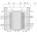
- FIG. 12 is a main part plan view of the MEMS scanner device 210 according to the third embodiment
- FIG. 13 is a perspective view showing an operation state in the rotational resonance mode.
- connection parts 18 and 20 which function as a plate-shaped hinge part have a structure which connected the three thin plate members in the meander shape.
- Other configurations are the same as those in the first embodiment. Since the number of thin plate members is large, a resonance frequency lower than that of the first embodiment can be obtained.
- the connecting portion 20 has a structure in which the thin plate members 219-4, 219-5, and 219-6 are arranged so as to be folded back in a meander shape.
- detection electrodes 225-3 and 225-4 are provided on odd-numbered thin plate members 219-3 and 219-4 from the side closer to the mirror section 12, and detection is performed on even-numbered thin plate members 219-2 and 219-5. Electrodes 225-2 and 225-5 are provided. For simplification of illustration, the wiring (51 to 54) and the output terminals (31 to 34) are not shown in FIG.
- the thin plate members denoted by reference numerals 219-1 and 219-6 correspond to “odd number”
- the thin plate members 219-1 and 219 ⁇ are replaced with or in combination with the detection electrodes 225-3 and 225-4.
- An embodiment in which a detection electrode is provided in 6 is also possible.
- the end portions 12A and 12B of the mirror portion 12 are vibrated up and down by the vertical drive of the piezoelectric actuator portions 14 and 16.
- an inclination (rotation) motion is induced in the mirror portion 12 by the inertial force, and the mirror portion 12 is largely inclined by the resonance vibration (see FIG. 13).
- serpentine connecting portions plate hinge portions folded in a meander shape
- the displacement of the tilt angle of the mirror portion 12 is further expanded. .
- produces in a connection part during rotational drive is detected, and the angle of the mirror part 12 can be grasped
- connecting portions 18 and 20 are meandering (meander-like) connecting portions, but one thin plate member that functions as a plate-like hinge.
- the form which comprises a connection part by is also possible.
- PZT is selected as the piezoelectric material used for the piezoelectric actuator unit and the sensor unit, but it is needless to say that the material is not limited to this material.
- a non-lead piezoelectric material such as BaTiO 3 , KaNaNbO 3 , or BiFeO 3 can be used, and a non-perovskite piezoelectric material such as AlN or ZnO 2 can also be used.
- a piezoelectric actuator portion in which a plurality of piezoelectric cantilevers are combined may be employed.
- a piezoelectric cantilever having a meander-like folded structure can be employed.
- the adoption of the folding structure of the cantilever part and the number of times of folding (the number of folding) are not particularly limited. The amount of displacement can be increased as the number of cantilever folds is increased.
- Design parameters such as the number of folding plate hinges and cantilevers and the width of the levers affect the overall resonance frequency.
- the resonance frequency tends to decrease as the number of folds increases. Further, the resonance frequency tends to decrease as the width of the lever portion or the plate-like member (hinge plate) is reduced.
- a desired resonance frequency can be realized by designing the number of folds, the lever portion, the width of the plate-like member (hinge plate), and the like.
- the present invention can be used in various applications as an optical device that reflects light such as laser light and changes the traveling direction of the light.
- optical deflectors optical scanning devices, laser printers, barcode readers, display devices, various optical sensors (ranging sensors, shape measuring sensors), optical communication devices, laser projectors, OCT diagnostic imaging devices, etc. can do.
Landscapes
- Physics & Mathematics (AREA)
- General Physics & Mathematics (AREA)
- Optics & Photonics (AREA)
- Chemical & Material Sciences (AREA)
- Engineering & Computer Science (AREA)
- Ceramic Engineering (AREA)
- Mechanical Optical Scanning Systems (AREA)
- Micromachines (AREA)
- Mechanical Light Control Or Optical Switches (AREA)
Priority Applications (2)
| Application Number | Priority Date | Filing Date | Title |
|---|---|---|---|
| EP13841383.6A EP2902836B1 (en) | 2012-09-26 | 2013-09-12 | Mirror driving device and driving method for same |
| US14/668,429 US10048489B2 (en) | 2012-09-26 | 2015-03-25 | Mirror driving device and driving method for same |
Applications Claiming Priority (2)
| Application Number | Priority Date | Filing Date | Title |
|---|---|---|---|
| JP2012212238A JP5916577B2 (ja) | 2012-09-26 | 2012-09-26 | ミラー駆動装置及びその駆動方法 |
| JP2012-212238 | 2012-09-26 |
Related Child Applications (1)
| Application Number | Title | Priority Date | Filing Date |
|---|---|---|---|
| US14/668,429 Continuation US10048489B2 (en) | 2012-09-26 | 2015-03-25 | Mirror driving device and driving method for same |
Publications (1)
| Publication Number | Publication Date |
|---|---|
| WO2014050586A1 true WO2014050586A1 (ja) | 2014-04-03 |
Family
ID=50387993
Family Applications (1)
| Application Number | Title | Priority Date | Filing Date |
|---|---|---|---|
| PCT/JP2013/074648 Ceased WO2014050586A1 (ja) | 2012-09-26 | 2013-09-12 | ミラー駆動装置及びその駆動方法 |
Country Status (4)
| Country | Link |
|---|---|
| US (1) | US10048489B2 (enExample) |
| EP (1) | EP2902836B1 (enExample) |
| JP (1) | JP5916577B2 (enExample) |
| WO (1) | WO2014050586A1 (enExample) |
Cited By (10)
| Publication number | Priority date | Publication date | Assignee | Title |
|---|---|---|---|---|
| JP5654158B1 (ja) * | 2014-05-07 | 2015-01-14 | 株式会社トライフォース・マネジメント | 可動反射素子および二次元走査装置 |
| WO2015191272A1 (en) * | 2014-06-12 | 2015-12-17 | LuxVue Technology Corporation | Micro pick up array pivot mount with integrated strain sensing elements |
| US20160069754A1 (en) * | 2014-09-05 | 2016-03-10 | Fraunhofer-Gesellschaft Zur Foerderung Der Angewandten Forschung E.V. | Piezoelectric position sensor for piezoelectrically driven resonant micromirrors |
| CN106794984A (zh) * | 2014-09-30 | 2017-05-31 | 苹果公司 | 用于应变放大的微型拾取阵列枢转安装件设计 |
| CN107533221A (zh) * | 2015-05-29 | 2018-01-02 | 三美电机株式会社 | 光扫描装置及其制造方法、光扫描控制装置 |
| KR20180015743A (ko) | 2015-06-09 | 2018-02-13 | 다이-이치 세이코 가부시키가이샤 | 가동 반사 장치 및 이것을 이용한 반사면 구동 시스템 |
| CN111289155A (zh) * | 2020-02-26 | 2020-06-16 | 西安交通大学 | 基于电磁激励压阻检测的面内振动硅微谐振式压力传感器 |
| CN112752209A (zh) * | 2019-10-31 | 2021-05-04 | 华为技术有限公司 | 一种压电式mems传感器以及相关设备 |
| CN115390237A (zh) * | 2022-08-25 | 2022-11-25 | 中国工程物理研究院激光聚变研究中心 | 一种等离子体电极变形镜 |
| CN119533756A (zh) * | 2024-11-18 | 2025-02-28 | 中电科芯片技术(集团)有限公司 | 一种低温漂mems谐振压力传感器敏感芯片及其制备方法 |
Families Citing this family (17)
| Publication number | Priority date | Publication date | Assignee | Title |
|---|---|---|---|---|
| US10739460B2 (en) | 2010-08-11 | 2020-08-11 | Apple Inc. | Time-of-flight detector with single-axis scan |
| CN104977104B (zh) * | 2015-07-13 | 2017-04-12 | 大连理工大学 | 一种压电式小量程大量程比的测力装置 |
| US10298913B2 (en) * | 2016-08-18 | 2019-05-21 | Apple Inc. | Standalone depth camera |
| IT201600132144A1 (it) * | 2016-12-29 | 2018-06-29 | St Microelectronics Srl | Dispositivo attuatore micro-elettro-meccanico con comando piezoelettrico, mobile nel piano |
| JP6354892B2 (ja) * | 2017-05-18 | 2018-07-11 | 株式会社リコー | 位置検出装置と映像機器 |
| EP3460981B1 (en) * | 2017-07-26 | 2022-03-30 | Tri-Force Management Corporation | Power generation element |
| DE102017220813A1 (de) * | 2017-11-22 | 2019-05-23 | Robert Bosch Gmbh | Laserprojektionsvorrichtung |
| JP6985602B2 (ja) * | 2018-01-29 | 2021-12-22 | ミツミ電機株式会社 | 光走査装置及び光走査装置の製造方法 |
| IT201800002364A1 (it) | 2018-02-02 | 2019-08-02 | St Microelectronics Srl | Dispositivo micro-manipolatore micro-elettro-meccanico con comando piezoelettrico, mobile nel piano |
| DE102018215528A1 (de) * | 2018-09-12 | 2020-03-12 | Robert Bosch Gmbh | Mikromechanisches Bauteil und Herstellungsverfahren für ein mikromechanisches Bauteil |
| US11221478B2 (en) * | 2019-04-15 | 2022-01-11 | Microsoft Technology Licensing, Llc | MEMS scanner |
| DE102019210033A1 (de) * | 2019-07-05 | 2021-01-07 | Robert Bosch Gmbh | Halbleiterbauelement |
| US11175492B2 (en) | 2019-08-12 | 2021-11-16 | Microsoft Technology Licensing, Llc | Substrate for scanning mirror system |
| US11750779B2 (en) | 2019-08-20 | 2023-09-05 | Ricoh Company, Ltd. | Light deflector, optical scanning system, image projection device, image forming apparatus, and lidar device |
| CN115298950A (zh) * | 2020-03-30 | 2022-11-04 | 松下知识产权经营株式会社 | 致动器以及光学反射元件 |
| US20220026537A1 (en) * | 2020-07-22 | 2022-01-27 | Beijing Voyager Technology Co., Ltd. | Systems and methods for sensing rotation angles of a micro mirror in an optical sensing system |
| CN115695956B (zh) * | 2021-07-30 | 2026-02-17 | 宁波舜宇光电信息有限公司 | 转动机构及其摄像模组 |
Citations (4)
| Publication number | Priority date | Publication date | Assignee | Title |
|---|---|---|---|---|
| JP2008040240A (ja) | 2006-08-08 | 2008-02-21 | Stanley Electric Co Ltd | 光偏向器及びその製造方法 |
| JP2009258210A (ja) * | 2008-04-14 | 2009-11-05 | Panasonic Corp | 光学反射素子 |
| JP2011095523A (ja) * | 2009-10-30 | 2011-05-12 | Panasonic Corp | 光学反射素子 |
| JP2011150055A (ja) | 2010-01-20 | 2011-08-04 | Stanley Electric Co Ltd | 光偏向器及びこれを用いた光学装置 |
Family Cites Families (6)
| Publication number | Priority date | Publication date | Assignee | Title |
|---|---|---|---|---|
| JP2008039810A (ja) * | 2006-08-01 | 2008-02-21 | Matsushita Electric Ind Co Ltd | 光学反射素子 |
| DE102007058239B4 (de) * | 2007-12-04 | 2021-04-29 | Robert Bosch Gmbh | Mikrospiegelvorrichtung |
| US8043313B2 (en) * | 2008-07-03 | 2011-10-25 | Hotspur Technologies, Inc | Apparatus and methods for treating obstructions within body lumens |
| US8477398B2 (en) * | 2009-05-11 | 2013-07-02 | Panasonic Corporation | Optical reflection element |
| JP5293668B2 (ja) * | 2010-03-30 | 2013-09-18 | パナソニック株式会社 | 光学反射素子 |
| JP5592192B2 (ja) * | 2010-08-11 | 2014-09-17 | 富士フイルム株式会社 | 圧電体膜とその製造方法、圧電素子および液体吐出装置 |
-
2012
- 2012-09-26 JP JP2012212238A patent/JP5916577B2/ja active Active
-
2013
- 2013-09-12 WO PCT/JP2013/074648 patent/WO2014050586A1/ja not_active Ceased
- 2013-09-12 EP EP13841383.6A patent/EP2902836B1/en active Active
-
2015
- 2015-03-25 US US14/668,429 patent/US10048489B2/en active Active
Patent Citations (4)
| Publication number | Priority date | Publication date | Assignee | Title |
|---|---|---|---|---|
| JP2008040240A (ja) | 2006-08-08 | 2008-02-21 | Stanley Electric Co Ltd | 光偏向器及びその製造方法 |
| JP2009258210A (ja) * | 2008-04-14 | 2009-11-05 | Panasonic Corp | 光学反射素子 |
| JP2011095523A (ja) * | 2009-10-30 | 2011-05-12 | Panasonic Corp | 光学反射素子 |
| JP2011150055A (ja) | 2010-01-20 | 2011-08-04 | Stanley Electric Co Ltd | 光偏向器及びこれを用いた光学装置 |
Non-Patent Citations (4)
| Title |
|---|
| JOURNAL OF MICROELECTROMECHANICAL SYSTEMS, vol. 15, no. 4, August 2006 (2006-08-01) |
| KOH, OPTICS EXPRESS, vol. 19, no. 15, 2011, pages 13812 |
| See also references of EP2902836A4 |
| T. ISEKI, IEEJ TRANS. ELEC. ELECTRON. ENG., vol. 5, 2010, pages 361 - 368 |
Cited By (19)
| Publication number | Priority date | Publication date | Assignee | Title |
|---|---|---|---|---|
| JP5654158B1 (ja) * | 2014-05-07 | 2015-01-14 | 株式会社トライフォース・マネジメント | 可動反射素子および二次元走査装置 |
| CN106461367B (zh) * | 2014-06-12 | 2020-03-17 | 苹果公司 | 具有集成应变感测元件的微型拾取阵列枢转底座 |
| WO2015191272A1 (en) * | 2014-06-12 | 2015-12-17 | LuxVue Technology Corporation | Micro pick up array pivot mount with integrated strain sensing elements |
| CN106461367A (zh) * | 2014-06-12 | 2017-02-22 | 苹果公司 | 具有集成应变感测元件的微型拾取阵列枢转底座 |
| US9624100B2 (en) | 2014-06-12 | 2017-04-18 | Apple Inc. | Micro pick up array pivot mount with integrated strain sensing elements |
| US10150669B2 (en) | 2014-06-12 | 2018-12-11 | Apple Inc. | Micro pick up array pivot mount |
| CN105405961A (zh) * | 2014-09-05 | 2016-03-16 | 弗劳恩霍夫应用研究促进协会 | 用于压电驱动共振微镜的压电式位置传感器 |
| US20160069754A1 (en) * | 2014-09-05 | 2016-03-10 | Fraunhofer-Gesellschaft Zur Foerderung Der Angewandten Forschung E.V. | Piezoelectric position sensor for piezoelectrically driven resonant micromirrors |
| US10101222B2 (en) | 2014-09-05 | 2018-10-16 | Fraunhofer-Gesellschaft Zur Foerderung Der Angewandten Forschung E.V. | Piezoelectric position sensor for piezoelectrically driven resonant micromirrors |
| CN106794984A (zh) * | 2014-09-30 | 2017-05-31 | 苹果公司 | 用于应变放大的微型拾取阵列枢转安装件设计 |
| CN107533221A (zh) * | 2015-05-29 | 2018-01-02 | 三美电机株式会社 | 光扫描装置及其制造方法、光扫描控制装置 |
| CN107533221B (zh) * | 2015-05-29 | 2020-05-19 | 三美电机株式会社 | 光扫描装置及其制造方法、光扫描控制装置 |
| US10473917B2 (en) | 2015-06-09 | 2019-11-12 | Dai-Ichi Seiko Co., Ltd. | Movable reflection device and reflection surface drive system utilizing same |
| KR20180015743A (ko) | 2015-06-09 | 2018-02-13 | 다이-이치 세이코 가부시키가이샤 | 가동 반사 장치 및 이것을 이용한 반사면 구동 시스템 |
| CN112752209A (zh) * | 2019-10-31 | 2021-05-04 | 华为技术有限公司 | 一种压电式mems传感器以及相关设备 |
| CN112752209B (zh) * | 2019-10-31 | 2022-03-25 | 华为技术有限公司 | 一种压电式mems传感器以及相关设备 |
| CN111289155A (zh) * | 2020-02-26 | 2020-06-16 | 西安交通大学 | 基于电磁激励压阻检测的面内振动硅微谐振式压力传感器 |
| CN115390237A (zh) * | 2022-08-25 | 2022-11-25 | 中国工程物理研究院激光聚变研究中心 | 一种等离子体电极变形镜 |
| CN119533756A (zh) * | 2024-11-18 | 2025-02-28 | 中电科芯片技术(集团)有限公司 | 一种低温漂mems谐振压力传感器敏感芯片及其制备方法 |
Also Published As
| Publication number | Publication date |
|---|---|
| JP2014066876A (ja) | 2014-04-17 |
| EP2902836A4 (en) | 2016-05-04 |
| EP2902836A1 (en) | 2015-08-05 |
| EP2902836B1 (en) | 2021-10-27 |
| JP5916577B2 (ja) | 2016-05-11 |
| US20150198801A1 (en) | 2015-07-16 |
| US10048489B2 (en) | 2018-08-14 |
Similar Documents
| Publication | Publication Date | Title |
|---|---|---|
| JP5916577B2 (ja) | ミラー駆動装置及びその駆動方法 | |
| JP5916667B2 (ja) | ミラー駆動装置及びその駆動方法 | |
| JP5323155B2 (ja) | ミラー駆動装置及びその駆動方法並びに製造方法 | |
| JP5916668B2 (ja) | ミラー駆動装置及びその駆動方法 | |
| JP5264954B2 (ja) | ミラー駆動装置及び方法 | |
| JP6308701B2 (ja) | ミラー駆動装置及びその駆動方法 | |
| JP6308700B2 (ja) | ミラー駆動装置及びその駆動方法 | |
| US9030721B2 (en) | Mirror driving device and method of controlling the device | |
| CN115461666A (zh) | 微镜器件 |
Legal Events
| Date | Code | Title | Description |
|---|---|---|---|
| 121 | Ep: the epo has been informed by wipo that ep was designated in this application |
Ref document number: 13841383 Country of ref document: EP Kind code of ref document: A1 |
|
| WWE | Wipo information: entry into national phase |
Ref document number: 2013841383 Country of ref document: EP |
|
| NENP | Non-entry into the national phase |
Ref country code: DE |