WO2014050586A1 - ミラー駆動装置及びその駆動方法 - Google Patents
ミラー駆動装置及びその駆動方法 Download PDFInfo
- Publication number
- WO2014050586A1 WO2014050586A1 PCT/JP2013/074648 JP2013074648W WO2014050586A1 WO 2014050586 A1 WO2014050586 A1 WO 2014050586A1 JP 2013074648 W JP2013074648 W JP 2013074648W WO 2014050586 A1 WO2014050586 A1 WO 2014050586A1
- Authority
- WO
- WIPO (PCT)
- Prior art keywords
- mirror
- piezoelectric actuator
- piezoelectric
- stress
- driving device
- Prior art date
Links
- 238000000034 method Methods 0.000 title claims description 37
- 238000001514 detection method Methods 0.000 claims description 115
- 230000000694 effects Effects 0.000 claims description 32
- 239000000463 material Substances 0.000 claims description 32
- 239000010409 thin film Substances 0.000 claims description 26
- 230000033001 locomotion Effects 0.000 claims description 18
- 239000000758 substrate Substances 0.000 claims description 13
- 230000008859 change Effects 0.000 claims description 11
- 238000004544 sputter deposition Methods 0.000 claims description 9
- 229910052758 niobium Inorganic materials 0.000 claims description 8
- 229910052760 oxygen Inorganic materials 0.000 claims description 7
- 229910052787 antimony Inorganic materials 0.000 claims description 6
- QVGXLLKOCUKJST-UHFFFAOYSA-N atomic oxygen Chemical compound [O] QVGXLLKOCUKJST-UHFFFAOYSA-N 0.000 claims description 6
- 239000001301 oxygen Substances 0.000 claims description 6
- 229910052715 tantalum Inorganic materials 0.000 claims description 6
- 229910052720 vanadium Inorganic materials 0.000 claims description 6
- 230000001747 exhibiting effect Effects 0.000 claims description 5
- 229910052719 titanium Inorganic materials 0.000 claims description 4
- 229910052726 zirconium Inorganic materials 0.000 claims description 4
- 229910052793 cadmium Inorganic materials 0.000 claims description 3
- 229910052804 chromium Inorganic materials 0.000 claims description 3
- 229910052802 copper Inorganic materials 0.000 claims description 3
- 229910052733 gallium Inorganic materials 0.000 claims description 3
- 229910052738 indium Inorganic materials 0.000 claims description 3
- 229910052742 iron Inorganic materials 0.000 claims description 3
- 229910052748 manganese Inorganic materials 0.000 claims description 3
- 229910052750 molybdenum Inorganic materials 0.000 claims description 3
- 229910052759 nickel Inorganic materials 0.000 claims description 3
- 229910052706 scandium Inorganic materials 0.000 claims description 3
- 229910052718 tin Inorganic materials 0.000 claims description 3
- 229910052721 tungsten Inorganic materials 0.000 claims description 3
- 229910052725 zinc Inorganic materials 0.000 claims description 3
- 230000010355 oscillation Effects 0.000 abstract 1
- 229910052451 lead zirconate titanate Inorganic materials 0.000 description 33
- 239000010408 film Substances 0.000 description 16
- 230000003287 optical effect Effects 0.000 description 14
- 238000006073 displacement reaction Methods 0.000 description 13
- 230000010287 polarization Effects 0.000 description 13
- 230000008569 process Effects 0.000 description 12
- 239000012071 phase Substances 0.000 description 10
- 238000010586 diagram Methods 0.000 description 8
- 238000004519 manufacturing process Methods 0.000 description 7
- RTAQQCXQSZGOHL-UHFFFAOYSA-N Titanium Chemical compound [Ti] RTAQQCXQSZGOHL-UHFFFAOYSA-N 0.000 description 6
- 238000013461 design Methods 0.000 description 6
- XUIMIQQOPSSXEZ-UHFFFAOYSA-N Silicon Chemical compound [Si] XUIMIQQOPSSXEZ-UHFFFAOYSA-N 0.000 description 5
- 230000015572 biosynthetic process Effects 0.000 description 5
- 229910052710 silicon Inorganic materials 0.000 description 5
- 239000010703 silicon Substances 0.000 description 5
- 238000005452 bending Methods 0.000 description 4
- 238000000151 deposition Methods 0.000 description 4
- 150000002500 ions Chemical class 0.000 description 4
- 238000005259 measurement Methods 0.000 description 4
- 238000012014 optical coherence tomography Methods 0.000 description 4
- 230000001419 dependent effect Effects 0.000 description 3
- HFGPZNIAWCZYJU-UHFFFAOYSA-N lead zirconate titanate Chemical compound [O-2].[O-2].[O-2].[O-2].[O-2].[Ti+4].[Zr+4].[Pb+2] HFGPZNIAWCZYJU-UHFFFAOYSA-N 0.000 description 3
- 238000012986 modification Methods 0.000 description 3
- 230000004048 modification Effects 0.000 description 3
- 230000035945 sensitivity Effects 0.000 description 3
- 238000003980 solgel method Methods 0.000 description 3
- ZOXJGFHDIHLPTG-UHFFFAOYSA-N Boron Chemical compound [B] ZOXJGFHDIHLPTG-UHFFFAOYSA-N 0.000 description 2
- 229910002113 barium titanate Inorganic materials 0.000 description 2
- 229910052796 boron Inorganic materials 0.000 description 2
- 150000001875 compounds Chemical class 0.000 description 2
- 239000013078 crystal Substances 0.000 description 2
- 230000006378 damage Effects 0.000 description 2
- 238000001312 dry etching Methods 0.000 description 2
- 239000007789 gas Substances 0.000 description 2
- 239000010931 gold Substances 0.000 description 2
- 238000009616 inductively coupled plasma Methods 0.000 description 2
- 229910052746 lanthanum Inorganic materials 0.000 description 2
- FZLIPJUXYLNCLC-UHFFFAOYSA-N lanthanum atom Chemical compound [La] FZLIPJUXYLNCLC-UHFFFAOYSA-N 0.000 description 2
- 229910052751 metal Inorganic materials 0.000 description 2
- 239000002184 metal Substances 0.000 description 2
- 238000000059 patterning Methods 0.000 description 2
- 238000005498 polishing Methods 0.000 description 2
- 238000012545 processing Methods 0.000 description 2
- 239000013077 target material Substances 0.000 description 2
- 238000001947 vapour-phase growth Methods 0.000 description 2
- 239000011701 zinc Substances 0.000 description 2
- DGAQECJNVWCQMB-PUAWFVPOSA-M Ilexoside XXIX Chemical compound C[C@@H]1CC[C@@]2(CC[C@@]3(C(=CC[C@H]4[C@]3(CC[C@@H]5[C@@]4(CC[C@@H](C5(C)C)OS(=O)(=O)[O-])C)C)[C@@H]2[C@]1(C)O)C)C(=O)O[C@H]6[C@@H]([C@H]([C@@H]([C@H](O6)CO)O)O)O.[Na+] DGAQECJNVWCQMB-PUAWFVPOSA-M 0.000 description 1
- 229910004298 SiO 2 Inorganic materials 0.000 description 1
- KPSZQYZCNSCYGG-UHFFFAOYSA-N [B].[B] Chemical compound [B].[B] KPSZQYZCNSCYGG-UHFFFAOYSA-N 0.000 description 1
- YPQJHZKJHIBJAP-UHFFFAOYSA-N [K].[Bi] Chemical compound [K].[Bi] YPQJHZKJHIBJAP-UHFFFAOYSA-N 0.000 description 1
- WOIHABYNKOEWFG-UHFFFAOYSA-N [Sr].[Ba] Chemical compound [Sr].[Ba] WOIHABYNKOEWFG-UHFFFAOYSA-N 0.000 description 1
- 230000001133 acceleration Effects 0.000 description 1
- 239000002253 acid Substances 0.000 description 1
- WYTGDNHDOZPMIW-RCBQFDQVSA-N alstonine Natural products C1=CC2=C3C=CC=CC3=NC2=C2N1C[C@H]1[C@H](C)OC=C(C(=O)OC)[C@H]1C2 WYTGDNHDOZPMIW-RCBQFDQVSA-N 0.000 description 1
- 229910052782 aluminium Inorganic materials 0.000 description 1
- XAGFODPZIPBFFR-UHFFFAOYSA-N aluminium Chemical compound [Al] XAGFODPZIPBFFR-UHFFFAOYSA-N 0.000 description 1
- JRPBQTZRNDNNOP-UHFFFAOYSA-N barium titanate Chemical compound [Ba+2].[Ba+2].[O-][Ti]([O-])([O-])[O-] JRPBQTZRNDNNOP-UHFFFAOYSA-N 0.000 description 1
- 230000009286 beneficial effect Effects 0.000 description 1
- 230000008901 benefit Effects 0.000 description 1
- 229910052797 bismuth Inorganic materials 0.000 description 1
- JCXGWMGPZLAOME-UHFFFAOYSA-N bismuth atom Chemical compound [Bi] JCXGWMGPZLAOME-UHFFFAOYSA-N 0.000 description 1
- FSAJRXGMUISOIW-UHFFFAOYSA-N bismuth sodium Chemical compound [Na].[Bi] FSAJRXGMUISOIW-UHFFFAOYSA-N 0.000 description 1
- 238000005229 chemical vapour deposition Methods 0.000 description 1
- 239000011248 coating agent Substances 0.000 description 1
- 238000000576 coating method Methods 0.000 description 1
- 238000004891 communication Methods 0.000 description 1
- 238000012790 confirmation Methods 0.000 description 1
- 230000008878 coupling Effects 0.000 description 1
- 238000010168 coupling process Methods 0.000 description 1
- 238000005859 coupling reaction Methods 0.000 description 1
- 230000008021 deposition Effects 0.000 description 1
- 238000002059 diagnostic imaging Methods 0.000 description 1
- NKZSPGSOXYXWQA-UHFFFAOYSA-N dioxido(oxo)titanium;lead(2+) Chemical compound [Pb+2].[O-][Ti]([O-])=O NKZSPGSOXYXWQA-UHFFFAOYSA-N 0.000 description 1
- 239000007772 electrode material Substances 0.000 description 1
- 238000005516 engineering process Methods 0.000 description 1
- 230000007613 environmental effect Effects 0.000 description 1
- 238000005530 etching Methods 0.000 description 1
- 238000011156 evaluation Methods 0.000 description 1
- 238000002474 experimental method Methods 0.000 description 1
- PCHJSUWPFVWCPO-UHFFFAOYSA-N gold Chemical compound [Au] PCHJSUWPFVWCPO-UHFFFAOYSA-N 0.000 description 1
- 229910052737 gold Inorganic materials 0.000 description 1
- 230000006872 improvement Effects 0.000 description 1
- 239000012212 insulator Substances 0.000 description 1
- 238000007733 ion plating Methods 0.000 description 1
- 238000010030 laminating Methods 0.000 description 1
- JQJCSZOEVBFDKO-UHFFFAOYSA-N lead zinc Chemical compound [Zn].[Pb] JQJCSZOEVBFDKO-UHFFFAOYSA-N 0.000 description 1
- QNZFKUWECYSYPS-UHFFFAOYSA-N lead zirconium Chemical compound [Zr].[Pb] QNZFKUWECYSYPS-UHFFFAOYSA-N 0.000 description 1
- GQYHUHYESMUTHG-UHFFFAOYSA-N lithium niobate Chemical compound [Li+].[O-][Nb](=O)=O GQYHUHYESMUTHG-UHFFFAOYSA-N 0.000 description 1
- 238000012544 monitoring process Methods 0.000 description 1
- 230000003071 parasitic effect Effects 0.000 description 1
- 238000001020 plasma etching Methods 0.000 description 1
- UKDIAJWKFXFVFG-UHFFFAOYSA-N potassium;oxido(dioxo)niobium Chemical compound [K+].[O-][Nb](=O)=O UKDIAJWKFXFVFG-UHFFFAOYSA-N 0.000 description 1
- 238000002310 reflectometry Methods 0.000 description 1
- 239000004065 semiconductor Substances 0.000 description 1
- 229910052708 sodium Inorganic materials 0.000 description 1
- 239000011734 sodium Substances 0.000 description 1
- 238000007740 vapor deposition Methods 0.000 description 1
- 238000000927 vapour-phase epitaxy Methods 0.000 description 1
- 238000001039 wet etching Methods 0.000 description 1
- 229910000859 α-Fe Inorganic materials 0.000 description 1
Images

Classifications
-
- G—PHYSICS
- G02—OPTICS
- G02B—OPTICAL ELEMENTS, SYSTEMS OR APPARATUS
- G02B26/00—Optical devices or arrangements for the control of light using movable or deformable optical elements
- G02B26/08—Optical devices or arrangements for the control of light using movable or deformable optical elements for controlling the direction of light
- G02B26/0816—Optical devices or arrangements for the control of light using movable or deformable optical elements for controlling the direction of light by means of one or more reflecting elements
- G02B26/0833—Optical devices or arrangements for the control of light using movable or deformable optical elements for controlling the direction of light by means of one or more reflecting elements the reflecting element being a micromechanical device, e.g. a MEMS mirror, DMD
- G02B26/0858—Optical devices or arrangements for the control of light using movable or deformable optical elements for controlling the direction of light by means of one or more reflecting elements the reflecting element being a micromechanical device, e.g. a MEMS mirror, DMD the reflecting means being moved or deformed by piezoelectric means
-
- G—PHYSICS
- G01—MEASURING; TESTING
- G01L—MEASURING FORCE, STRESS, TORQUE, WORK, MECHANICAL POWER, MECHANICAL EFFICIENCY, OR FLUID PRESSURE
- G01L1/00—Measuring force or stress, in general
- G01L1/16—Measuring force or stress, in general using properties of piezoelectric devices
-
- G—PHYSICS
- G01—MEASURING; TESTING
- G01L—MEASURING FORCE, STRESS, TORQUE, WORK, MECHANICAL POWER, MECHANICAL EFFICIENCY, OR FLUID PRESSURE
- G01L1/00—Measuring force or stress, in general
- G01L1/16—Measuring force or stress, in general using properties of piezoelectric devices
- G01L1/162—Measuring force or stress, in general using properties of piezoelectric devices using piezoelectric resonators
-
- G—PHYSICS
- G01—MEASURING; TESTING
- G01L—MEASURING FORCE, STRESS, TORQUE, WORK, MECHANICAL POWER, MECHANICAL EFFICIENCY, OR FLUID PRESSURE
- G01L1/00—Measuring force or stress, in general
- G01L1/18—Measuring force or stress, in general using properties of piezo-resistive materials, i.e. materials of which the ohmic resistance varies according to changes in magnitude or direction of force applied to the material
-
- G—PHYSICS
- G02—OPTICS
- G02B—OPTICAL ELEMENTS, SYSTEMS OR APPARATUS
- G02B26/00—Optical devices or arrangements for the control of light using movable or deformable optical elements
- G02B26/08—Optical devices or arrangements for the control of light using movable or deformable optical elements for controlling the direction of light
- G02B26/10—Scanning systems
- G02B26/105—Scanning systems with one or more pivoting mirrors or galvano-mirrors
-
- H—ELECTRICITY
- H10—SEMICONDUCTOR DEVICES; ELECTRIC SOLID-STATE DEVICES NOT OTHERWISE PROVIDED FOR
- H10N—ELECTRIC SOLID-STATE DEVICES NOT OTHERWISE PROVIDED FOR
- H10N30/00—Piezoelectric or electrostrictive devices
- H10N30/20—Piezoelectric or electrostrictive devices with electrical input and mechanical output, e.g. functioning as actuators or vibrators
- H10N30/204—Piezoelectric or electrostrictive devices with electrical input and mechanical output, e.g. functioning as actuators or vibrators using bending displacement, e.g. unimorph, bimorph or multimorph cantilever or membrane benders
- H10N30/2041—Beam type
- H10N30/2042—Cantilevers, i.e. having one fixed end
- H10N30/2044—Cantilevers, i.e. having one fixed end having multiple segments mechanically connected in series, e.g. zig-zag type
-
- H—ELECTRICITY
- H10—SEMICONDUCTOR DEVICES; ELECTRIC SOLID-STATE DEVICES NOT OTHERWISE PROVIDED FOR
- H10N—ELECTRIC SOLID-STATE DEVICES NOT OTHERWISE PROVIDED FOR
- H10N30/00—Piezoelectric or electrostrictive devices
- H10N30/80—Constructional details
- H10N30/85—Piezoelectric or electrostrictive active materials
- H10N30/853—Ceramic compositions
- H10N30/8548—Lead based oxides
- H10N30/8554—Lead zirconium titanate based
Definitions
- the present invention relates to a mirror driving device, and more particularly to a structure of a micromirror device suitable for an optical deflector used for optical scanning and a driving method thereof.
- a micro scanner (hereinafter referred to as a “MEMS (Micro Electro Mechanical System) scanner”) manufactured using silicon (Si) microfabrication technology is smaller and lower in size than a polygon mirror, which is a conventional optical scanning module. It is characterized by power consumption. For this reason, MEMS scanners are expected to have a wide range of applications, from laser projectors to optical diagnostic scanners such as optical coherence tomography (OCT).
- OCT optical coherence tomography
- a torsion bar system as shown in Patent Documents 1 and 2 is generally used.
- two or three or more torsion bars supporting the mirror are twisted to tilt the mirror and perform optical scanning.
- resonance driving is performed.
- the structure is designed so that the resonance frequency of the tilting motion of the mirror matches the driving frequency.
- Non-Patent Document 1 an angle sensor using a piezoresistive effect is provided at the base of the torsion bar
- Non- Patent Document 2 an angle sensor using a piezoelectric effect of a piezo thin film is used
- the torsion bar acting as a spring must be made extremely fragile. There is no problem.
- low frequency driving 400 Hz (hertz) or less is performed. If this is to be realized by the torsion bar method, for example, it is necessary to process Si with a thickness of 5 ⁇ m (micrometer), a width of 10 ⁇ m, and a length of 600 ⁇ m to form a torsion bar. Since this is a very fragile structure, there is a problem that it is easily destroyed when an impact is applied during the manufacturing process or during device driving. Further, an increase in the length of the torsion bar leads to an increase in the size of the element.
- Non-patent Document 3 As a design suitable for low-frequency driving, an example using a leaf spring structure (plate hinge) folded in a meander shape has been proposed (Non-patent Document 3).
- the structure shown in Non-Patent Document 3 can keep the resonance frequency low by connecting a plurality of leaf springs so as to be folded in a meander shape.
- each leaf spring has a structure with higher rigidity than that of a torsion bar, and is not easily broken by external vibration.
- Non-Patent Document 3 the conventional angle sensor shown in Non-Patent Documents 1 and 2 cannot be applied, and it is difficult to sense the angle. Therefore, a circuit that follows resonance cannot be incorporated, and it has been difficult to put it into practical use.
- the present invention has been made in view of such circumstances, and provides a mirror driving device that is small in size, can realize a large mirror tilt angle (rotation angle) at a low driving frequency, and has an angle sensing function, and a driving method thereof.
- the purpose is to do.
- a mirror driving device includes a mirror part having a reflecting surface for reflecting light, a pair of piezoelectric actuator parts arranged on both sides of the mirror part, and a rotation axis of the mirror part
- a connecting portion that connects one end of the piezoelectric actuator portion to the end portion of the mirror portion that is away from the rotating surface along the reflecting surface in a direction perpendicular to the rotation axis, and a fixing portion that supports the other end of the piezoelectric actuator portion.
- the portion has a structure including one or more plate-like members whose longitudinal direction is perpendicular to the rotation axis along the reflecting surface, and the plate-like member is bent and deformed in the thickness direction by driving the piezoelectric actuator portion.
- the connecting part has a stress detecting part for detecting the stress generated in the connecting part during the rotational driving of the mirror part due to the resonance vibration accompanied by the rotational movement of the mirror part induced by the driving of the piezoelectric actuator part. Setting It is.
- the pair of piezoelectric actuator portions are arranged so as to sandwich the mirror portion from both sides.
- One end of the piezoelectric actuator part is connected to the end part of the mirror part via the connecting part, and the other end is supported by the fixed part.
- the piezoelectric actuator unit is driven, the end of the mirror unit is displaced, and the resonance of the rotational motion is induced by the inertia torque, so that a large rotation angle (mirror tilt angle) can be obtained.
- the plate-like member of the connecting portion that functions as the plate-like hinge portion is bent (bent) in the thickness direction during the rotational drive of the mirror portion by this resonance, and the stress corresponding to this deformation is detected by the stress detection portion.
- the stress detection portion can function as an angle sensor. .
- the connecting portion has a structure in which two or more plate-like members are arranged so as to be folded back in a meander shape, and the plates arranged next to each other. It can be set as the structure which bends and deform
- each plate-like hinge portion composed of a plurality of plate-like members connected in a meander shape, it is easy to design to keep the resonance frequency low. Further, since each plate-like member can have a structure with relatively high rigidity, it becomes a structure that is not easily destroyed by external vibration.
- two or more plate-like members arranged so as to be folded back in a meander shape are arranged in the direction from the side close to the mirror portion toward the piezoelectric actuator portion.
- a first stress detection unit that detects a stress generated in an odd-numbered plate-shaped member and an even-numbered plate-shaped member as a stress detection unit when specifying each plate-shaped member by giving a sequential number indicating the order
- a second stress detection unit for detecting the stress generated in the.
- the stress detection unit is a laminate in which a lower electrode, a piezoelectric body, and an upper electrode are sequentially laminated on a plate-like member. It has a structure, and it can be set as the structure which converts stress into an electric signal by the piezoelectric effect of a piezoelectric material.
- the stress applied to the plate-like member can be detected as a voltage between the upper electrode and the lower electrode, and can function as an angle sensor.
- the detection sensitivity can be improved and the signal / noise ratio (S / N ratio) can be improved.
- the stress detection unit is formed of a material in which a surface portion of the plate-like member exhibits a piezoresistance effect, and the piezoresistance It can be set as the structure which converts stress into the change of resistance value by the piezoresistive effect of the material which shows an effect.
- the means for detecting the stress applied to the connecting portion is not limited to the configuration using the piezoelectric effect, and a configuration using the piezoresistance effect can be employed.
- the mirror driving device may include a detection circuit that converts a change in resistance value into a voltage signal.
- the detection circuit is configured by a first resistor and a second stress detection unit configured by the first stress detection unit.
- the voltage signal can be obtained by a voltage dividing circuit connected to the second resistor.
- the piezoelectric actuator unit includes a piezoelectric unimorph cantilever in which a diaphragm, a lower electrode, a piezoelectric body, and an upper electrode are stacked in this order. It can consist of.
- the piezoelectric cantilever is not limited to a unimorph structure but can also be a bimorph structure, but the unimorph structure is the simplest configuration. Since the piezoelectric drive system can be driven simply by applying a voltage between the electrodes, the structure is simple and it is beneficial for miniaturization.
- the piezoelectric body used in the piezoelectric actuator section and the stress detection section is a thin film having a thickness of 1 to 10 ⁇ m, It can be a thin film directly formed on the substrate.
- the piezoelectric actuator part and the stress detection part can be manufactured by the same process.
- a piezoelectric thin film having a required piezoelectric performance can be obtained by using a direct film formation method such as a vapor phase growth method represented by a sputtering method or a sol-gel method.
- a direct film formation method such as a vapor phase growth method represented by a sputtering method or a sol-gel method.
- the piezoelectric body used in the piezoelectric actuator unit is one or two kinds represented by the following formula (P):
- the above perovskite oxide can be obtained.
- General formula ABO 3 (P) (In the formula, A: an element of A site, and at least one element including Pb.
- O Oxygen element.
- the molar ratio of the A site element, the B site element, and the oxygen element is 1: 1: 3 as a standard, but these molar ratios may deviate from the reference molar ratio within a range where a perovskite structure can be taken. ) Note that the same piezoelectric material as that of the piezoelectric actuator unit can be used for the piezoelectric body used in the stress detection unit.
- the piezoelectric body used in the piezoelectric actuator unit is one or two kinds represented by the following formula (PX)
- PX The above perovskite oxide can be obtained.
- A (Zr x , Ti y , M bxy ) b O c (PX)
- A an element of A site, and at least one element including Pb.
- M At least one element selected from the group consisting of V, Nb, Ta, and Sb. 0 ⁇ x ⁇ b, 0 ⁇ y ⁇ b, 0 ⁇ b ⁇ xy.
- PZT doped with an element such as Nb has a high piezoelectric constant, it is suitable for manufacturing a small device capable of obtaining a large displacement. Note that the same piezoelectric material as that of the piezoelectric actuator unit can be used for the piezoelectric body used in the stress detection unit.
- the perovskite oxide (PX) contains Nb, and the Nb / (Zr + Ti + Nb) molar ratio is 0.06 or more and 0.20 or less. It is preferable to do.
- Such a material exhibits good piezoelectric properties without performing polarization treatment. Therefore, the polarization process is unnecessary, and the manufacturing process can be simplified and the cost can be reduced.
- the piezoelectric body used in the piezoelectric actuator portion can be a thin film formed by sputtering.
- the driving circuit for supplying a driving voltage for resonantly driving the mirror unit in the vicinity of the resonance frequency fx of the resonance mode in which the rotary motion is performed can be provided.
- a mirror driving method in the mirror driving device according to any one of the first to fifteenth aspects, wherein a driving voltage is applied to a pair of piezoelectric actuator parts to vibrate the piezoelectric actuator parts.
- a mirror driving method including vibrating the connecting portion between the mirror portion and the coupling portion, applying a rotational torque around the rotation axis to the mirror portion by the vibration, and driving the mirror portion to resonate.
- the driving voltage or the driving frequency applied to the piezoelectric actuator unit is controlled using a detection signal obtained from the stress detecting unit during the resonance driving of the mirror unit. Can further be included.
- At least one of the frequency (drive frequency) and amplitude of the drive voltage supplied to the piezoelectric actuator unit can be controlled based on the detection signal obtained from the stress detection unit.
- a stable resonance drive can be realized by feeding back a detection signal obtained from the stress detection unit to the drive of the piezoelectric actuator unit.
- a mirror driving device that is smaller than a conventional torsion bar system, can realize a large mirror tilt angle (rotation angle) with a low driving frequency, and is equipped with an angle sensing function.
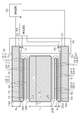
- FIG. 1 is a perspective view of the MEMS scanner device according to the first embodiment.
- FIG. 2 is an explanatory diagram combining a plan view of the MEMS scanner device of FIG. 1 viewed from the reflection surface side of the mirror portion and a block configuration diagram showing circuit elements.
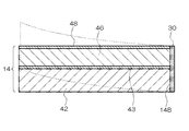
- FIG. 3 is a cross-sectional view of the piezoelectric actuator portion.
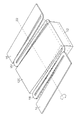
- FIG. 4 is a perspective view showing a state during driving in the rotational resonance mode.
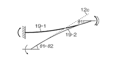
- FIG. 5 is a schematic view of the first connecting portion (plate hinge) shown in FIG. 4 as viewed from the positive direction of the y-axis.
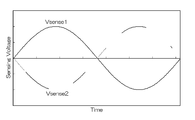
- FIG. 6 is a diagram illustrating an example of an angle detection signal obtained by detecting the stress of the connecting portion.
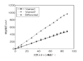
- FIG. 7 is a graph showing the relationship between the optical scan angle and the detection voltage.
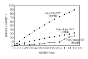
- FIG. 8 is a graph showing the relationship between the applied voltage and the optical scan angle.
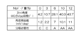
- FIG. 9 is a chart summarizing the relationship between the Nb doping amount in PZT and the actuator characteristics / sensing characteristics.
- FIG. 10 is a plan view showing the configuration of the MEMS scanner device according to the second embodiment.
- FIG. 11 is a diagram illustrating a configuration example of a detection circuit applied to the second embodiment.
- FIG. 12 is a plan view showing the configuration of the MEMS scanner device according to the third embodiment.
- FIG. 13 is a perspective view showing a state during driving in the rotational resonance mode in the third embodiment.
- FIG. 1 is a perspective view of the MEMS scanner device according to the first embodiment.
- FIG. 2 is a combination of a plan view (top view) of the MEM scanner device according to the first embodiment viewed from the reflection surface side of the mirror unit and a block configuration diagram showing circuit elements for device driving and angle detection.
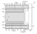
- the MEMS scanner device 10 (corresponding to a “mirror drive device”) of this example includes a mirror unit 12 and a pair of piezoelectric actuator units 14 disposed on both sides of the mirror unit 12. , 16, connecting portions 18, 20 that connect one end portion 14 ⁇ / b> A, 16 ⁇ / b> A of each piezoelectric actuator portion 14, 16 and the end portions 12 ⁇ / b> A, 12 ⁇ / b> B of the mirror portion 12, and the other end portion of the piezoelectric actuator portions 14, 16. (Hereinafter, referred to as a base end portion) 14B and 16B.
- the piezoelectric actuator part 14 may be referred to as a “first piezoelectric actuator part”, and the piezoelectric actuator part 16 may be referred to as a “second piezoelectric actuator part”.
- the connection part 18 is referred to as a “first connection part”
- the connection part 20 is referred to as a “second connection part”
- the end part 12 ⁇ / b> A is referred to as a “first end part”
- the end part 12 ⁇ / b> B is referred to as an end part.
- second end Sometimes referred to as “second end”.
- the mirror part 12 of this example is substantially rectangular in a plan view as shown in the figure, and the mirror surface (the upper surface of the mirror part 12) that becomes the reflection surface 12C that reflects light is used to increase the reflectance of incident light.
- a metal thin film such as Au (gold) or Al (aluminum) is formed.
- the material and film thickness used for the mirror coating are not particularly limited, and various designs are possible using a known mirror material (high reflectivity material).
- rectangular is not limited to a strict rectangular shape (rectangular shape), but means a shape that can be generally grasped as a rectangular shape as an overall basic shape.
- a rectangular corner portion is chamfered, a corner portion is rounded, a part or all of a side is formed by a curve or a broken line, a connecting portion between the mirror portion 12 and each of the connecting portions 18 and 20
- additional shapes necessary for connection are added.
- the shape of the mirror portion 12 is not particularly limited. Not only the rectangle illustrated in FIGS. 1 and 2 but also various shapes such as a square, a polygon, a circle, and an ellipse can be used. Further, the planar view shape of the mirror part 12 and the shape of the reflection surface 12C may be the same or different.
- the reflection surface 12 ⁇ / b> C can be formed within the area of the upper surface of the mirror portion 12.
- the mirror part 12 having a substantially rectangular reflecting surface 12C in plan view is illustrated, the long side direction of the mirror part 12 when not driven is in the x direction, the short side direction orthogonal to this is the y direction, and the xy plane An orthogonal xyz axis with the direction perpendicular to z as the z direction will be described.
- the MEMS scanner device 10 has a pair of piezoelectric actuator portions 14 and 16 disposed so that the mirror portion 12 with the reflecting surface 12C facing in the z-axis direction is sandwiched from both sides in the y-axis direction when not driven.
- Each of the piezoelectric actuator units 14 and 16 is an actuator having a piezoelectric unimorph cantilever (cantilever) structure (see FIG. 3), and performs bending displacement by deformation of the piezoelectric body due to the inverse piezoelectric effect. That is, the piezoelectric actuator portions 14 and 16 are fixedly supported by the fixed frame 30 at one end in the x direction (base ends 14B and 16B), and the opposite end portions 14A and 16A are not fixed to the frame or the like. It is an unconstrained end that can be displaced by the cantilever structure.
- the end portion 14A on the non-constraining side of the first piezoelectric actuator portion 14 is connected to one end portion 18A of the first connecting portion 18 configured in a meander shape.
- the other end portion 18B of the first connecting portion 18 is connected to the first end portion 12A on the side of the mirror portion 12 along the x-axis direction.
- the non-constrained end 16A of the second piezoelectric actuator section 16 is connected to one end 20A of the second connecting section 20 configured in a meander shape.
- the other end 20B of the second connecting portion 20 is connected to the second end 12B in the x-axis direction of the mirror portion 12.
- the end portions (12A, 12B) in the x-axis direction of the mirror portion 12 to which the first connecting portion 18 and the second connecting portion 20 are respectively connected are not required to be the extreme end positions in a strict sense, and generally It includes a part of a range (the extreme end position and the vicinity thereof) that can be grasped as an end part.
- the MEMS scanner device 10 of this example drives the first piezoelectric actuator unit 14 and the second piezoelectric actuator unit 16 to move the end portions (12A, 12B) of the mirror unit 12 up and down (in the thickness direction of the mirror unit 12).
- the mirror unit 12 is excited to rotate and revolve around the rotation axis 22 parallel to the y-axis, thereby driving the mirror unit 12 to rotate (see FIG. 4).
- the rotation axis 22 is a straight line that passes through substantially the center point of the reflecting surface 12C and is parallel to the y-axis.
- the first connecting portion 18 and the second connecting portion 20 are connected to a portion in the vicinity of the end portion of the mirror portion 12 that is separated from the mirror center in the x-axis direction within a range in which such a target resonance drive can be achieved. That is, the first end portion 12A and the second end portion 12B of the mirror portion 12 to which the first connecting portion 18 and the second connecting portion 20 are connected are in the x-axis direction (rotating axis) from the rotating shaft 22 along the reflecting surface 12C. This is a portion including the range of the vicinity of the end of the mirror portion 12 and the vicinity of the end of the mirror portion 12 that is separated in a direction perpendicular to the uppermost portion 22.
- the first connecting portion 18 and the second connecting portion 20 have a structure in which a plurality of flat plate-like thin plate members 19 (corresponding to “plate-like members”) whose longitudinal direction is the x-axis direction are arranged in a meander shape.
- a structure in which two thin plate members 19 are arranged in parallel and end portions of these two thin plate members 19 are connected so as to be folded back in a meander shape is not particularly limited, and may be one or more and an appropriate number.
- the first connecting portion 18 and the second connecting portion 20 drive the first piezoelectric actuator portion 14 and the second piezoelectric actuator portion 16, respectively, so that each thin plate member 19 is bent (bent) and deformed in the thickness direction. Function as.
- the mirror portion 12 is subjected to acceleration directions (force is applied to the end portions 14A and 16A of the piezoelectric actuator portions 14 and 16). Inertia force in the opposite direction works. Since this inertial force coincides with the direction in which the mirror unit 12 is tilted, the force generated by the piezoelectric actuator units 14 and 16 is efficiently used as the force for tilting the mirror unit 12.
- each of the connecting units 18 and 20 is associated with the displacement of the piezoelectric actuator units 14 and 16.
- the thin plate member 19 bends (bends), and inertia torque is generated in the mirror portion 12 to induce rotational motion resonance of the mirror portion 12.
- the displacement direction of the piezoelectric actuator parts 14 and 16 always coincides with the rotation direction of the mirror part 12 and all the force is used for rotation of the mirror, the use efficiency of the force is much better than that of the torsion bar structure, Even if the rotation angle increases, a large displacement (inclination angle) can be obtained because there is little energy loss.
- each thin plate member 19 bends little by little and accumulates displacement, so that the stress applied to each thin plate member 19 is increased. There is an advantage that it is less likely to be destroyed even when the rotation angle is high.
- the plurality of thin plate members 19 constituting the first connecting portion 18 and the second connecting portion 20 are sequentially directed from the left in FIG. 1 toward the right (from the top to the bottom in FIG. 2). ), The first thin plate member 19-1, the second thin plate member 19-2, the third thin plate member 19-3, and the fourth thin plate member 19-4.
- the first connecting portion 18 is configured by connecting the first thin plate member 19-1 and the second thin plate member 19-2.
- the second connecting portion 20 is configured by connecting a third thin plate member 19-3 and a fourth thin plate member 19-4.
- Numerals 31, 32, 33, and 34 provided on the surface of the fixed frame 30 in the drawing are output terminals for detection signal output.
- Each wiring 51 to 54 is patterned on the piezoelectric film.
- the wiring 51 drawn from the detection electrode 25-1 formed on the upper surface of the first thin plate member 19-1 is located alongside the upper electrode (drive electrode 15) of the first piezoelectric actuator section 14 from the first thin plate member 19-1. Is routed along the longitudinal direction and connected to the output terminal (first output terminal) indicated by reference numeral 31.
- the wiring 52 drawn from the detection electrode 25-2 formed on the upper surface of the second thin plate member 19-2 is routed along the longitudinal direction alongside the detection electrode 25-1 of the first thin plate member 19-1.
- the side of the upper electrode (drive electrode 15) of the first piezoelectric actuator unit 14 is routed along the longitudinal direction and connected to the output terminal (second output terminal) indicated by reference numeral 32.
- the wiring 53 drawn from the detection electrode 25-3 formed on the upper surface of the third thin plate member 19-3 is routed along the longitudinal direction alongside the detection electrode 25-4 of the fourth thin plate member 19-4. At the same time, it is routed along the longitudinal direction along the upper electrode (drive electrode 17) of the second piezoelectric actuator section 16, and is connected to an output terminal (third output terminal) indicated by reference numeral 33.
- the wiring 54 drawn from the detection electrode 25-4 formed on the fourth thin plate member 19-4 is located beside the upper electrode (drive electrode 17) of the second piezoelectric actuator section 16 from the fourth thin plate member 19-4. Is routed along the longitudinal direction and connected to an output terminal (fourth output terminal) indicated by reference numeral 34.
- the first piezoelectric actuator unit 14 and the second piezoelectric actuator unit 16 are connected to the drive circuit 62 via a wiring member such as wire bonding.
- FIG. 3 is a schematic diagram showing a cross-sectional structure of the piezoelectric actuator portions 14 and 16 having a piezoelectric unimorph cantilever structure. Since the piezoelectric actuator portions 14 and 16 have the same structure, the structure of the piezoelectric actuator portion denoted by reference numeral 14 will be described as a representative. In implementing the present invention, a structure other than a unimorph cantilever may be used as the piezoelectric actuator portion. For example, you may use the bimorph cantilever which laminated
- the piezoelectric actuator unit 14 has a structure in which a lower electrode 43, a piezoelectric body 46, and an upper electrode 48 are stacked on a vibration plate 42.
- a laminated structure can be obtained, for example, by sequentially depositing the lower electrode 43, the piezoelectric body 46, and the upper electrode 48 on a silicon (Si) substrate.
- the right end in FIG. 3 is a fixed end supported by a fixed frame 30 (see FIGS. 1 and 2).
- the piezoelectric body 46 is deformed by applying a drive voltage between the electrodes (43, 48), and the diaphragm 42 is bent along with this deformation, and the lever portion moves up and down.
- a broken line in FIG. 3 represents a state in which the lever portion is displaced upward.
- the piezoelectric actuator units 14 and 16 are means for converting an electrical signal into a mechanical displacement using the inverse piezoelectric effect of the piezoelectric body 46.
- the same drive voltage is simultaneously applied to the pair of piezoelectric actuator units 14 and 16 from the drive circuit 62 to displace the piezoelectric actuator units 14 and 16 on both sides of the mirror unit 12 in the same direction.
- a common (same) drive circuit 62 can be used as a power supply source for supplying drive power to the pair of piezoelectric actuator units 14 and 16.
- a sine waveform signal or a pulse waveform signal having a frequency for exciting resonance can be used as a sine waveform signal or a pulse waveform signal having a frequency for exciting resonance.
- the MEMS scanner device 10 operates as follows.
- the piezoelectric actuator units 14 and 16 are vibrated up and down to induce a rotational motion in the mirror unit 12.
- the mirror unit 12 vibrates with a large tilt angle by applying a drive voltage having a frequency near the resonance frequency to drive resonance.
- the meander-like connecting portions 18 and 20 are easily bent and deformed, it is effective to obtain a large displacement in resonance driving (see FIGS. 4 and 5).
- the frequency of the drive voltage applied to the piezoelectric actuator sections 14 and 16 is not necessarily required to exactly match the mechanical resonance frequency of the structure. A difference in the frequency of the drive voltage is allowed in a range where resonance is excited.
- the mirror part 12 can be displaced with a large rotation angle around the rotation axis 22 by this rotational resonance drive. That is, according to the driving of the piezoelectric actuator units 14 and 16, the central mirror unit 12 is swung around the rotation shaft 22. Light incident on the reflecting surface 12C of the mirror unit 12 (for example, laser light emitted from a laser light source (not shown)) is reflected according to the inclination (angle) of the mirror unit 12, and the traveling direction of the reflected light (the reflected light) (Irradiation position) changes. According to the MEMS scanner device 10 according to the present embodiment, optical scanning can be performed with a large deflection angle.
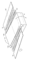
- FIG. 4 and 5 are explanatory diagrams for explaining the stress ( ⁇ xx component) related to the connecting portion (plate hinge portion) during resonance driving.
- FIG. 4 is a perspective view showing a state during driving in the rotational resonance mode
- FIG. 5 is a schematic view of the first connecting portion 18 shown in FIG. 4 viewed from the positive direction of the y-axis.
- the illustration of the fixed frame 30 is omitted.
- the movement of the second connecting portion 20 is the same as the movement of the first connecting portion 18 due to the symmetry of the device structure.
- the thin plate members 19-1 and 19-2 constituting the first connecting portion 18 are bent and deformed in opposite directions to each other, and the respective thin plate members 19-1, 19- Stress acts on the surface of 2 in opposite directions. That is, as shown in FIG. 5, when the first thin plate member 19-1 moves downward (curvature deformation), the second thin plate member 19-2 moves upward. At this time, compressive stress is applied to the surface of the first thin plate member 19-1, and tensile stress is applied to the surface of the second thin plate member 19-2.
- first thin plate member 19-1 (hinge 1) and second thin plate member 19-2 (hinge 2) bend in the opposite directions, and the angular displacement ⁇ 1 due to the bending of the first thin plate member 19-1.
- the angle displacement ⁇ 2 due to the bending of the second thin plate member 19-2 is added to obtain the tilt angle of the mirror portion 12.
- the reflecting surface 12C of the mirror unit 12 is inclined at an angle of ( ⁇ 1 + ⁇ 2) around the y axis.
- the stress on the first thin plate member 19-1 and the second thin plate member 19-2 is detected as the voltage between the upper and lower electrodes of the sensor units 24-1 and 24-2 by the piezoelectric effect, and the angle It functions as a sensor.
- an AGC Automatic Gain Control
- PLL phase-locked loop
- Such a feedback control circuit can be incorporated in the detection circuit 64.
- the drive circuit 62, the detection circuit 64, and the feedback control circuit can be collectively configured by an integrated circuit such as an ASIC (Application Specific Specific Integrated Circuit).
- a sensor portion may be provided in a part of the thin plate member 19, and a detection electrode having an appropriate size can be designed.
- the area of the detection electrode of the sensor unit is relatively small from the viewpoint of relatively reducing the influence of the parasitic capacitance component / resistance component of the subsequent stage such as the wiring unit A relatively large size is desirable.
- Examples of the piezoelectric body suitable for the present embodiment include those containing one or more perovskite oxides (P) represented by the following formula.
- ABO 3 (P) (In the formula, A: an element of A site, and at least one element including Pb.
- O Oxygen element.
- the molar ratio of the A site element, the B site element, and the oxygen element is 1: 1: 3 as a standard, but these molar ratios may deviate from the reference molar ratio within a range where a perovskite structure can be taken.
- Perovskite oxides represented by the above general formula include lead titanate, lead zirconate titanate (PZT), lead zirconate, lead lanthanum titanate, lead lanthanum zirconate titanate, lead zirconium titanate niobate , Lead-containing compounds such as lead zirconium niobate titanate titanate and lead zinc niobate titanate titanate, and mixed crystals thereof; barium titanate, strontium barium titanate, bismuth sodium titanate, bismuth potassium titanate, niobic acid Non-lead-containing compounds such as sodium, potassium niobate, lithium niobate, bismuth ferrite, and mixed crystals thereof can be mentioned.
- PZT lead zirconate titanate
- lead lanthanum titanate lead lanthanum zirconate titanate
- lead zirconium titanate niobate Lead-containing compounds such as lead zirconium niobate titan
- the piezoelectric film of the present embodiment preferably includes one or more perovskite oxides (PX) represented by the following formula.
- A (Zr x , Ti y , M b-xy ) b O c (PX)
- A an element of A site, and at least one element including Pb.
- M is at least one element selected from the group consisting of V, Nb, Ta, and Sb. 0 ⁇ x ⁇ b, 0 ⁇ y ⁇ b, 0 ⁇ b ⁇ xy.
- the perovskite oxide (PX) is an intrinsic PZT or a part of the B site of PZT substituted with M. It is known that PZT to which various donor ions having a valence higher than that of the substituted ion are added has improved characteristics such as piezoelectric performance as compared with intrinsic PZT.
- M is preferably one or more donor ions having a valence higher than that of tetravalent Zr or Ti. Examples of such donor ions include V 5+ , Nb 5+ , Ta 5+ , Sb 5+ , Mo 6+ , and W 6+ .
- Bxy is not particularly limited as long as it has a perovskite structure.
- M is Nb
- the Nb / (Zr + Ti + Nb) molar ratio is preferably 0.05 or more and 0.25 or less, and more preferably 0.06 or more and 0.20 or less.
- the piezoelectric film made of the perovskite oxide represented by the above general formulas (P) and (PX) has a high piezoelectric strain constant (d31 constant), the piezoelectric actuator provided with such a piezoelectric film is displaced. Excellent characteristics.
- the piezoelectric actuator provided with the piezoelectric film made of the perovskite oxide represented by the general formulas (P) and (PX) has voltage-displacement characteristics with excellent linearity. These piezoelectric materials exhibit good actuator characteristics and sensor characteristics in practicing the present invention. Note that the perovskite oxide represented by the general formula (PX) has a higher piezoelectric constant than that represented by the general formula (P).
- a lead zirconate titanate (PZT) thin film doped with 12% of Nb in atomic composition percentage can be used.
- a bulk piezoelectric body may be bonded to the substrate and polished.
- the piezoelectric body 46 of the present embodiment is preferably a thin film having a thickness of 1 ⁇ m or more and 10 ⁇ m or less.
- Vapor phase epitaxy is preferred as the piezoelectric film formation method.
- various methods such as ion plating, MOCVD (metal organic chemical vapor deposition), and PLD (pulse laser deposition) can be applied in addition to sputtering. It is also conceivable to use a method other than the vapor phase growth method (for example, a sol-gel method).
- Example 1 which will be described later, a PZT thin film having a thickness of 4 ⁇ m formed by sputtering is used as the piezoelectric body 46, but is not limited thereto.
- Example 1 an example of a specific manufacturing method> As Example 1, a MEMS scanner device 10 was manufactured by the following procedure.
- Step 1 On a SOI (Silicon On Insulator) substrate having a handle layer of 350 ⁇ m, a box layer of 1 ⁇ m, and a device layer of 10 ⁇ m, a Ti layer of 30 nm and an Ir electrode layer of 150 nm were formed by a sputtering method at a substrate temperature of 350 ° C. These Ti layer and Ir electrode layer correspond to the lower electrode 43 in FIG.
- SOI Silicon On Insulator
- Step 2 A PZT layer having a thickness of 4 ⁇ m was formed on the obtained substrate using a radio frequency (RF) sputtering apparatus.
- a film forming gas was a mixed gas of 97.5% Ar and 2.5% O 2 , and a target material having a composition of Pb 1.3 ((Zr 0.52 Ti 0.48 ) 0.88 Nb 0.12 ) O 3 was used.
- the film forming pressure was 2.2 mTorr (about 0.293 Pa), and the film forming temperature was 450 ° C.
- the obtained PZT layer was an Nb-doped PZT thin film in which Nb was added at 12% by atomic composition ratio.
- Step 3 A Pt / Ti layer as an upper electrode was patterned on the substrate obtained above by lift-off, and the PZT thin film was pattern etched by ICP (inductively coupled plasma) dry etching.
- ICP inductively coupled plasma
- Step 4 the device layer was pattern-etched by a silicon dry etch process, and the handle layer was deep-etched (Deep RIE; Reactive Ion Etching) from the back surface. Finally, by removing the Box-SiO 2 layer from the back surface, a piezoelectric MEMS scanner device configured as shown in FIG. 1 was produced.
- the fixed frame 30 has a structure using both the handle layer and the device layer, and has a thickness of about 360 ⁇ m.
- Both the piezoelectric actuator part and the plate-like hinge part have a laminated structure of Si device layer (10 ⁇ m) / lower electrode / PZT thin film / upper electrode.
- the piezoelectric actuator unit functions as a piezoelectric thin film unimorph actuator that bends up and down when a voltage is applied between the upper and lower electrodes.
- Piezoelectric actuators 14 and 16 have a laminated structure of Si device layer (10 ⁇ m) / lower electrode / PZT thin film / upper electrode and function as a piezoelectric thin film unimorph actuator.
- Example 1 a PZT thin film is formed directly on a substrate by a sputtering method, and then dry-etched.
- the creation process can be simplified and fine patterning can be performed.
- the yield can be significantly improved and further miniaturization of the device can be accommodated.
- the configuration for implementing the present invention is not limited to a thin film piezoelectric body, but a unimorph actuator is formed by pasting a bulk piezoelectric body to a diaphragm, or a bimorph actuator by pasting two piezoelectric bodies having different polarities. It is also good.
- the substrate material, the electrode material, the piezoelectric material, the film thickness, the film forming conditions, and the like can be appropriately selected according to the purpose without being limited to the first embodiment.
- Example 1 ⁇ Evaluation of MEMS Scanner Device According to Example 1>
- a rotational resonance motion around the rotation axis of the mirror was induced, and the mechanical shake angle of the mirror portion was measured by the laser scan angle.
- the resonance frequency fx was 154 Hz and the mechanical shake angle was ⁇ 22 °.
- a voltage output with a potential amplitude of 470 mV (millivolts) was obtained from 25-1 and 25-4, a voltage output with a potential amplitude of 490 mV was obtained from the detection electrodes 25-2 and 25-3, and the phase difference between these signals was 180 °. (See FIG. 7).
- Vsense1 indicates signals from the detection electrodes 25-1 and 25-4
- Vsense2 indicates signals from the detection electrodes 25-2 and 25-3.
- FIG. 7 shows a plot of the relationship between the scan angle and the detection voltage by changing the drive voltage applied to the piezoelectric actuator sections 14 and 16.
- “Differential” indicates that the difference between the two voltage signals (Vsense1, Vsense2) is detected by the difference circuit.
- the angle detection ability of each detection electrode was as follows.
- Vsense1 5.41 mV / deg
- Vsense2 5.61 mV / deg Difference: 11 mV / deg
- the MEMS scanner device 10 shown in FIG. 1 has a symmetrical structure with the mirror portion 12 interposed therebetween, and the first thin plate member 19-1 and the fourth thin plate member 19-2 are at resonance drive. Are equivalent movements, and the second thin plate member 19-2 and the third thin plate member 19-3 are equivalent movements.
- the same detection signal (Vsense1 in FIG. 6) is obtained from the sensor unit 24-1 on the first thin plate member 19-1 and the sensor unit 24-4 on the fourth thin plate member 19-4.
- a similar detection signal (Vsense2 in FIG. 6) is obtained from the sensor portion 24-2 on the second thin plate member 19-2 and the sensor portion 24-3 on the third thin plate member 19-3.
- a combination of the third thin plate member 19-3, a combination of the second thin plate member 19-2 and the fourth thin plate member 19-4, and a combination of the third thin plate member 19-3 and the fourth thin plate member 19-4 are also possible. Any combination may be adopted.
- the number of thin plate members constituting the meander-like connecting portions (18, 20) is generalized as m (m is an integer of 2 or more), the m thin plate members are outward from the side closer to the mirror portion 12.
- the initial value of the serial number j is not limited to “1”, and may be “0”, and may be an arbitrary integer.
- a sensor unit that detects a stress generated in at least one thin plate member selected from among the odd-numbered thin plate members, and a stress generated in at least one thin plate member selected from among the even-numbered thin plate members. What is necessary is just to detect a signal from both of these sensor parts as a structure provided with a sensor part.
- Example 2 In Example 2, the same production method as in Example 1 was used except that a target material at the time of PZT film formation was Pb 1.3 ((Zr 0.52 Ti 0.48 ) O 3 ). The MEMS scanner device having the structure was manufactured, and an operation confirmation experiment was performed on the obtained device in the same manner as in Example 1. Fig. 8 shows the relationship between the applied voltage and the optical scan angle. The results of Example 1 (Nb12% PZT) are also shown.
- the white triangles in FIG. 8 are the results of measurement without performing polarization treatment on PZT not doped with Nb.
- the black triangles are the measurement results when PZT not doped with Nb is polarized after film formation.
- the black circles are the measurement results of Example 1 using PZT doped with 12% Nb (no polarization treatment).
- FIG. 9 shows a table summarizing the relationship between the Nb doping amount in PZT and the actuator characteristics / sensing characteristics.
- unpolarized values are used for both the scan angle and the angle detection capability.
- the determination regarding the necessity of the polarization process is “C” (the polarization process is necessary) when the scan angle in the unpolarized state (when 0.5 Vpp is applied) is 0.8 or less of the scan angle after the polarization process. , 0.8 and 0.9 or less, “A” (can be used in unpolarized treatment), and 0.9 above “AA” (no polarization treatment required).
- the PZT can be used without performing polarization treatment by doping Nb with 6% or more, the manufacturing cost can be reduced.
- the higher the Nb doping amount the higher the scan angle can be obtained at a lower voltage, and the higher detection voltage can be obtained during angle detection.
- the stress applied to the connecting portions 18 and 20 during the rotational motion is detected as a voltage signal by the piezoelectric effect.
- the angle of the mirror part 12 can be grasped from this voltage signal.
- a MEMS scanner device can be formed by directly forming a PZT thin film on a substrate and etching it. As described above, since the fine patterning can be easily performed by thinning the piezoelectric body, the yield can be greatly improved and the device can be further miniaturized.
- a structure in which a piezoelectric thin film is laminated on the connecting portions 18 and 20 functioning as a plate-like hinge portion and stress is converted into a voltage by the piezoelectric effect is used.
- the means for detecting the stress is not limited to this example.
- a form using the piezoresistive effect as means for detecting the stress generated in the connecting portion is also possible.
- boron (boron) doping is performed on the surfaces of the connecting portions 18 and 20 of silicon (Si) to form a p-type Si layer exhibiting a piezoresistive effect, and the electric resistance of the p-type Si layer depends on the applied stress. You may employ
- FIG. 10 is a plan view showing the configuration of the MEMS scanner device according to the second embodiment. 10, elements that are the same as or similar to those in FIGS. 1 and 2 are given the same reference numerals, and descriptions thereof are omitted.
- the stress is detected using.
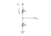
- FIG. 11 is a configuration diagram of a circuit that converts a change in resistance value into a voltage.
- R1 and R2 in the figure indicate the resistances of the piezoresistive material portions provided on the thin plate members that are displaced in opposite directions. That is, R1 represents the resistance of the piezoresistive material portion provided in the odd-numbered thin plate member (for example, the resistance of the piezoresistive material portion 125-3 provided in the third thin plate member 19-3), and R2 represents The resistance of the piezoresistive material portion provided in the even-numbered thin plate member (for example, the resistance of the piezoresistive material portion 125-4 provided in the fourth thin plate member 19-4) is shown.
- a voltage dividing circuit in which R1 and R2 are connected is configured, and a voltage signal Vout divided by R1 and R2 is obtained.
- a circuit is incorporated in the detection circuit 64.
- the piezoresistive effect is temperature dependent, the temperature dependent component of the resistance change is canceled by using a voltage dividing circuit as shown in FIG.
- the actuator part and the sensor part can be collectively formed in the same process, so that the process becomes simple and the cost can be reduced.
- the piezoelectric effect is less temperature dependent than the piezoresistive effect, and a voltage signal can be obtained directly between the electrodes, so that the configuration of the detection circuit is simple.
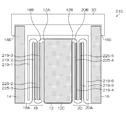
- FIG. 12 is a main part plan view of the MEMS scanner device 210 according to the third embodiment
- FIG. 13 is a perspective view showing an operation state in the rotational resonance mode.
- connection parts 18 and 20 which function as a plate-shaped hinge part have a structure which connected the three thin plate members in the meander shape.
- Other configurations are the same as those in the first embodiment. Since the number of thin plate members is large, a resonance frequency lower than that of the first embodiment can be obtained.
- the connecting portion 20 has a structure in which the thin plate members 219-4, 219-5, and 219-6 are arranged so as to be folded back in a meander shape.
- detection electrodes 225-3 and 225-4 are provided on odd-numbered thin plate members 219-3 and 219-4 from the side closer to the mirror section 12, and detection is performed on even-numbered thin plate members 219-2 and 219-5. Electrodes 225-2 and 225-5 are provided. For simplification of illustration, the wiring (51 to 54) and the output terminals (31 to 34) are not shown in FIG.
- the thin plate members denoted by reference numerals 219-1 and 219-6 correspond to “odd number”
- the thin plate members 219-1 and 219 ⁇ are replaced with or in combination with the detection electrodes 225-3 and 225-4.
- An embodiment in which a detection electrode is provided in 6 is also possible.
- the end portions 12A and 12B of the mirror portion 12 are vibrated up and down by the vertical drive of the piezoelectric actuator portions 14 and 16.
- an inclination (rotation) motion is induced in the mirror portion 12 by the inertial force, and the mirror portion 12 is largely inclined by the resonance vibration (see FIG. 13).
- serpentine connecting portions plate hinge portions folded in a meander shape
- the displacement of the tilt angle of the mirror portion 12 is further expanded. .
- produces in a connection part during rotational drive is detected, and the angle of the mirror part 12 can be grasped
- connecting portions 18 and 20 are meandering (meander-like) connecting portions, but one thin plate member that functions as a plate-like hinge.
- the form which comprises a connection part by is also possible.
- PZT is selected as the piezoelectric material used for the piezoelectric actuator unit and the sensor unit, but it is needless to say that the material is not limited to this material.
- a non-lead piezoelectric material such as BaTiO 3 , KaNaNbO 3 , or BiFeO 3 can be used, and a non-perovskite piezoelectric material such as AlN or ZnO 2 can also be used.
- a piezoelectric actuator portion in which a plurality of piezoelectric cantilevers are combined may be employed.
- a piezoelectric cantilever having a meander-like folded structure can be employed.
- the adoption of the folding structure of the cantilever part and the number of times of folding (the number of folding) are not particularly limited. The amount of displacement can be increased as the number of cantilever folds is increased.
- Design parameters such as the number of folding plate hinges and cantilevers and the width of the levers affect the overall resonance frequency.
- the resonance frequency tends to decrease as the number of folds increases. Further, the resonance frequency tends to decrease as the width of the lever portion or the plate-like member (hinge plate) is reduced.
- a desired resonance frequency can be realized by designing the number of folds, the lever portion, the width of the plate-like member (hinge plate), and the like.
- the present invention can be used in various applications as an optical device that reflects light such as laser light and changes the traveling direction of the light.
- optical deflectors optical scanning devices, laser printers, barcode readers, display devices, various optical sensors (ranging sensors, shape measuring sensors), optical communication devices, laser projectors, OCT diagnostic imaging devices, etc. can do.
Abstract
ミラー駆動装置を提供する。ミラー部を挟んで両側に一対の圧電アクチュエータ部が配置され、ミラー部の端部に連結部を介して圧電アクチュエータ部が接続される。連結部は、回転軸に垂直な方向を長手方向とする板状部材を1本以上含んだ構造を有し、圧電アクチュエータ部の駆動によって板状部材が厚み方向に撓み変形する板状ヒンジ部として機能する。連結部には、共振振動によるミラー部の回転駆動中に連結部に発生する応力を検出するセンサ部が設けられている。
Description
本発明はミラー駆動装置に係り、特に、光走査に用いる光偏向器に好適なマイクロミラーデバイスの構造及びその駆動方法に関する。
シリコン(Si)の微細加工技術を用いて作製されたマイクロスキャナ(以下、「MEMS(Micro Electro Mechanical System)スキャナ」という。)は、従来の光走査モジュールであるポリゴンミラーなどと比べて小型かつ低消費電力であることが特徴である。このためMEMSスキャナは、レーザープロジェクタから光干渉断層計(OCT;Optical Coherence Tomography)のような光診断用スキャナなど、幅広い応用が期待されている。
MEMSスキャナの構造としては、特許文献1、2などに示されるようなトーションバー方式が一般的である。この方式では、ミラーを支える2本または3本以上のトーションバーがねじられることによってミラーが傾き、光スキャンを行う。特に高いスキャン角度を実現するためには、共振駆動を行う。この場合、ミラーの傾き運動の共振周波数が駆動の周波数と一致するように構造設計される。
また、MEMSスキャナの駆動においては、ミラーの角度をモニタリングしたり、共振状態を維持したりする目的で、ミラーの角度をセンシングできる角度センサを設ける構成が知られている。従来のトーションバー方式のMEMSスキャナに関してトーションバーの根本の部分にピエゾ抵抗効果を用いた角度センサを設ける構成(非特許文献1)や、ピエゾ薄膜の圧電効果を用いた角度センサを用いる構成(非特許文献2)が提案されており、一部が実用化されている。
JOURNAL OF MICROELECTROMECHANICAL SYSTEMS, VOL. 15, NO. 4, AUGUST 2006
T. Iseki et. al., IEEJ Trans. Elec. Electron. Eng. 2010, 5, pp. 361-368.
Koh et. al., OPTICS EXPRESS Vol.19 No.15 (2011) 13812
以上に述べたように、高いスキャン角度を持つMEMSスキャナを実用化するためには、設計上次の2点を満たすことが望まれる。
(1)構造の共振周波数を駆動周波数と一致させる。
(2)角度センサを実装する。
しかしながら、比較的低い周波数で駆動する用途の場合、構造の共振周波数を低くする必要があり、これをトーションバー方式で設計しようとすると、バネの役割を果たすトーションバーを極端に脆弱にせざるを得ないという問題がある。一例として、OCTなどの光による測定を行いながらスキャンを実施する用途では、400Hz(ヘルツ)以下の低周波数駆動が行われる。これをトーションバー方式で実現しようとすると、例えば、厚み5μm(マイクロメートル)、幅10μm、長さ600μmの寸法でSiを加工してトーションバーを形成する必要がある。これは非常に脆弱な構造であるため、製造プロセス中やデバイス駆動中など衝撃などが加わると容易に破壊されてしまうという問題がある。また、トーションバーの長さ寸法が増加することで素子の大型化も招いてしまう。
その一方で、低周波数駆動に適した設計として、ミアンダ(meander)状に折りたたんだ板バネ構造(板状ヒンジ)を用いる例も提案されている(非特許文献3)。非特許文献3に示された構造は、複数の板バネをミアンダ状に複数折りたたむように繋ぎ合わせたことによって共振周波数を低く抑えることができる。また、一つ一つの板バネはトーションバーの場合よりも剛性が高い構造となるため、外的振動によって破壊されにくい。
しかしながら、非特許文献3に示された構造では、非特許文献1、2に示された従来の角度センサを適用できず、角度をセンシングすることが難しい。そのため、共振を追随する回路などを組み込むことができず、実用化するのが困難であった。
本発明はこのような事情に鑑みてなされたもので、小型で、低い駆動周波数で大きなミラー傾斜角度(回転角)を実現でき、かつ角度センシング機能を搭載したミラー駆動装置及びその駆動方法を提供することを目的とする。
前記目的を達成するために、次の発明を提供する。
(第1態様):第1態様に係るミラー駆動装置は、光を反射する反射面を有するミラー部と、ミラー部を挟んで両側に配置される一対の圧電アクチュエータ部と、ミラー部の回転軸から反射面に沿って回転軸に垂直な方向に離れたミラー部の端部に圧電アクチュエータ部の一端を接続させる連結部と、圧電アクチュエータ部の他端を支持する固定部と、を備え、連結部は、反射面に沿って回転軸に垂直な方向を長手方向とする板状部材を1本以上含んだ構造を有し、圧電アクチュエータ部の駆動によって板状部材が厚み方向に撓み変形する板状ヒンジ部であり、連結部には、圧電アクチュエータ部の駆動によって誘起されるミラー部の回転運動を伴う共振振動によるミラー部の回転駆動中に連結部に発生する応力を検出する応力検出部が設けられている。
この態様によれば、ミラー部を両側から挟むように一対の圧電アクチュエータ部が配置される。圧電アクチュエータ部の一端は連結部を介してミラー部の端部に接続され、他端は固定部に支持される。圧電アクチュエータ部を駆動するとミラー部の端部が変位し、慣性トルクにより回転運動の共振が誘起され、大きな回転角(ミラーの傾き角)を得ることができる。この共振によるミラー部の回転駆動中に板状ヒンジ部として機能する連結部の板状部材は厚み方向に撓み(曲がり)変形し、この変形に応じた応力が応力検出部によって検出される。連結部の変形量とミラー部の角度は一定の対応関係があり、また連結部の変形量と連結部にかかる応力にも対応関係があるため、応力検出部を角度センサとして機能させることができる。なお、複数本の板状部材を備える構成の場合、少なくとも1つの板状部材について応力検出部を備えていればよい。
(第2態様):第1態様に記載のミラー駆動装置において、連結部は、2本以上の板状部材がミアンダ状に折り返すように並べられた構造を有しており、隣り合って並ぶ板状部材同士が共振振動のときに互いに逆方向に撓み変形する構成とすることができる。
複数本の板状部材をミアンダ状に繋ぎ合わせた構造からなる板状ヒンジ部を採用することにより、共振周波数を低く抑える設計が容易である。また、一つ一つの板状部材は比較的剛性が高い構造とすることが可能であるため、外的振動に破壊されにくい構造となる。
(第3態様):第2態様に記載のミラー駆動装置において、ミアンダ状に折り返すように並べられた2本以上の板状部材について、ミラー部に近い側から圧電アクチュエータ部の方向に向かって並び順を示す連続番号を与えてそれぞれの板状部材を特定するときに、応力検出部として、奇数番目の板状部材に発生する応力を検出する第1応力検出部と、偶数番目の板状部材に発生する応力を検出する第2応力検出部と、を備える構成とすることが好ましい。
奇数番目の板状部材と偶数番目の板状部材とは、共振駆動中に互いに逆方向の応力が加わるため、これらを組み合わせて検出を行うことで、検出感度の向上や検出精度の向上が可能となる。
(第4態様):第1態様から第3態様のいずれか1項に記載のミラー駆動装置において、応力検出部は、板状部材上に下部電極、圧電体、上部電極の順に積層された積層構造を有し、圧電体の圧電効果によって応力を電気信号に変換する構造とすることができる。
この態様によれば、板状部材にかかる応力を上部電極と下部電極の間の電圧として検出し、角度センサとして機能させることができる。
(第5態様):第3態様を採用するときの第4態様に記載のミラー駆動装置において、第1応力検出部及び第2応力検出部の両方からそれぞれ電圧信号が得られ、第1応力検出部から得られる第1検出信号と第2応力検出部から得られる第2検出信号の差分を検出する検出回路を備える構成とすることが好ましい。
特に、互いに逆位相(位相差が180°)の第1検出信号、第2検出信号を得て、両者の差分をとることで、検出感度の向上を達成できるとともに、シグナル/ノイズ比(S/N比)の向上を達成できる。
(第6態様):第1態様から第3態様のいずれか1項に記載のミラー駆動装置において、応力検出部は、板状部材の表面部がピエゾ抵抗効果を示す材料で構成され、ピエゾ抵抗効果を示す材料のピエゾ抵抗効果によって応力を抵抗値の変化に変換する構成とすることができる。
連結部にかかる応力を検出する手段としては、圧電効果を利用する構成に限らず、ピエゾ抵抗効果を利用する構成を採用することができる。
(第7態様):第6態様に記載のミラー駆動装置において、抵抗値の変化を電圧信号に変換する検出回路を備える構成とすることができる。
ピエゾ抵抗効果を示す材料に電流を流し、抵抗値に応じた電圧の情報を得ることができる。
(第8態様):第3態様を採用するときの第7態様に記載のミラー駆動装置において、検出回路は、第1応力検出部で構成される第1抵抗と第2応力検出部で構成される第2抵抗とを接続した分圧回路によって電圧信号を得る構成とすることができる。
かかる態様によれば、ピエゾ抵抗効果の温度依存性の影響を除去した検出が可能である。
(第9態様):第1態様から第8態様のいずれか1項に記載のミラー駆動装置において、圧電アクチュエータ部は、振動板、下部電極、圧電体、上部電極の順に積層された圧電ユニモルフカンチレバーで構成されるものとすることができる。
圧電カンチレバーは、ユニモルフ構造に限らず、バイモルフ構造も可能であるが、ユニモルフ構造が最も簡単な構成である。圧電駆動方式は、電極間に電圧を印加するだけで駆動できるため、構成が単純で小型化に有益である。
(第10態様):第4態様を採用するときの第9態様に記載のミラー駆動装置において、圧電アクチュエータ部及び応力検出部に用いられる圧電体は1~10μm厚の薄膜であり、振動板となる基板上に直接成膜された薄膜とすることができる。
かかる態様によれば、圧電アクチュエータ部と応力検出部とを同一のプロセスで作製することが可能である。また、スパッタリング法に代表される気相成長法やゾルゲル法などの直接成膜法を用いることにより、所要の圧電性能を持つ圧電体薄膜を得ることができる。基板に圧電体の薄膜を直接成膜し、ドライエンチング若しくはウエットエッチングなどの半導体プロセスで加工することで、デバイスの作製プロセスを簡便にできる。
(第11態様):第1態様から第10態様のいずれか1項に記載のミラー駆動装置において、圧電アクチュエータ部に用いられる圧電体は、下記式(P)で表される1種又は2種以上のペロブスカイト型酸化物とすることができる。
一般式ABO3・・・(P)
(式中、A:Aサイトの元素であり、Pbを含む少なくとも1種の元素。
B:Bサイトの元素であり、Ti,Zr,V,Nb,Ta,Sb,Cr,Mo,W,Mn,Sc,Co,Cu,In,Sn,Ga,Zn,Cd,Fe,及びNiからなる群より選ばれた少なくとも1種の元素。
O:酸素元素。
Aサイト元素とBサイト元素と酸素元素のモル比は1:1:3が標準であるが、これらのモル比はペロブスカイト構造を取り得る範囲内で基準モル比からずれてもよい。)
なお、応力検出部に用いる圧電体についても、圧電アクチュエータ部と同じ圧電材料を用いることができる。
一般式ABO3・・・(P)
(式中、A:Aサイトの元素であり、Pbを含む少なくとも1種の元素。
B:Bサイトの元素であり、Ti,Zr,V,Nb,Ta,Sb,Cr,Mo,W,Mn,Sc,Co,Cu,In,Sn,Ga,Zn,Cd,Fe,及びNiからなる群より選ばれた少なくとも1種の元素。
O:酸素元素。
Aサイト元素とBサイト元素と酸素元素のモル比は1:1:3が標準であるが、これらのモル比はペロブスカイト構造を取り得る範囲内で基準モル比からずれてもよい。)
なお、応力検出部に用いる圧電体についても、圧電アクチュエータ部と同じ圧電材料を用いることができる。
(第12態様):第1態様から第10態様のいずれか1項に記載のミラー駆動装置において、圧電アクチュエータ部に用いられる圧電体は、下記式(PX)で表される1種又は2種以上のペロブスカイト型酸化物とすることができる。
Aa(Zrx,Tiy,Mb-x-y)bOc・・・(PX)
(式中、A:Aサイトの元素であり、Pbを含む少なくとも1種の元素。
M:V,Nb,Ta,及びSbからなる群より選ばれた少なくとも1種の元素である。
0<x<b、0<y<b、0≦b-x-y。
a:b:c=1:1:3が標準であるが、これらのモル比はペロブスカイト構造を取り得る範囲内で基準モル比からずれてもよい。)
Nb等の元素をドープしたPZTは圧電定数が高いため、小型で大きな変位が得られるデバイスの作製に好適である。なお、応力検出部に用いる圧電体についても、圧電アクチュエータ部と同じ圧電材料を用いることができる。
(式中、A:Aサイトの元素であり、Pbを含む少なくとも1種の元素。
M:V,Nb,Ta,及びSbからなる群より選ばれた少なくとも1種の元素である。
0<x<b、0<y<b、0≦b-x-y。
a:b:c=1:1:3が標準であるが、これらのモル比はペロブスカイト構造を取り得る範囲内で基準モル比からずれてもよい。)
Nb等の元素をドープしたPZTは圧電定数が高いため、小型で大きな変位が得られるデバイスの作製に好適である。なお、応力検出部に用いる圧電体についても、圧電アクチュエータ部と同じ圧電材料を用いることができる。
(第13態様):第12態様に記載のミラー駆動装置において、ペロブスカイト型酸化物(PX)は、Nbを含み、Nb/(Zr+Ti+Nb)モル比が0.06以上0.20以下であるものとすることが好ましい。
かかる材料は、分極処理を行わなくても良好な圧電特性を示す。したがって、分極処理が不要であり、製造プロセスの簡略化、低コスト化を実現できる。
(第14態様):第1態様から第13態様に記載のミラー駆動装置において、圧電アクチュエータ部に用いられる圧電体はスパッタリング法で成膜された薄膜とすることができる。
(第15態様):第1態様から第14態様のいずれか1項に記載のミラー駆動装置において、一対の圧電アクチュエータ部に駆動電圧を供給する駆動回路であって、ミラー部が回転軸を中心に回転運動を行う共振モードの共振周波数fxの付近でミラー部を共振駆動させる駆動電圧を供給する駆動回路を備える構成とすることができる。
かかる態様によれば、回転共振を利用してミラー部を大きな回転角で振動させることができる。
(第16態様):第1態様から第15態様のいずれか1項に記載のミラー駆動装置におけるミラー駆動方法であって、一対の圧電アクチュエータ部に駆動電圧を印加し、圧電アクチュエータ部を振動させることと、ミラー部と連結部との接続部分を振動させ、この振動によりミラー部に回転軸周りの回転トルクを与え、ミラー部を共振駆動させることを含む、ミラー駆動方法。
(第17態様):第16態様に記載のミラー駆動方法において、ミラー部の共振駆動中に応力検出部から得られる検出信号を用いて圧電アクチュエータ部に印加する駆動電圧もしくは駆動周波数を制御することを更に含むことができる。
例えば、応力検出部から得られる検出信号に基づいて、圧電アクチュエータ部に供給する駆動電圧の周波数(駆動周波数)、振幅のうち少なくとも一方を制御する構成とすることができる。応力検出部から得られる検出信号を圧電アクチュエータ部の駆動にフィードバックすることにより、安定した共振駆動を実現できる。
本発明によれば、従来のトーションバー方式に比べて、小型で、低い駆動周波数によって大きなミラー傾斜角度(回転角)を実現でき、かつ角度センシング機能を搭載したミラー駆動装置を提供することができる。
以下、添付図面に従って本発明の実施形態について詳説する。
<第1実施形態>
図1は第1実施形態に係るMEMSスキャナデバイスの斜視図である。図2は第1実施形態に係るMEMスキャナデバイスをミラー部の反射面側から見た平面図(上面図)とデバイス駆動及び角度検出のための回路要素を示したブロック構成図とを組み合わせた説明図である。
図1は第1実施形態に係るMEMSスキャナデバイスの斜視図である。図2は第1実施形態に係るMEMスキャナデバイスをミラー部の反射面側から見た平面図(上面図)とデバイス駆動及び角度検出のための回路要素を示したブロック構成図とを組み合わせた説明図である。
これらの図面に示したように、本例のMEMSスキャナデバイス10(「ミラー駆動装置」に相当)は、ミラー部12と、該ミラー部12を挟んで両側に配置される一対の圧電アクチュエータ部14、16と、各圧電アクチュエータ部14、16の一方の端部14A、16Aとミラー部12の端部12A、12Bとを繋ぐ連結部18、20と、圧電アクチュエータ部14、16の他方の端部(以下、基端部という。)14B、16Bが固定支持される固定フレーム30(「固定部」に相当)と、を備える。
説明の便宜上、符号14の圧電アクチュエータ部を「第1圧電アクチュエータ部」、符号16の圧電アクチュエータ部を「第2圧電アクチュエータ部」という場合がある。また符号18の連結部を「第1連結部」、符号20の連結部を「第2連結部」という場合があり、符号12Aの端部を「第1端部」、符号12Bの端部を「第2端部」という場合がある。
本例のミラー部12は、図示のように平面視で略矩形であり、光を反射する反射面12Cとなるミラー面(ミラー部12の上面)には、入射光の反射率を高めるために、Au(金)やAl(アルミ)等の金属薄膜が形成されている。ミラーコーティングに用いる材料や膜厚は特に限定されず、公知のミラー材料(高反射率材料)を用いて様々な設計が可能である。
ミラー部12の形状について「矩形」とは厳密な矩形(四角形)に限らず、全体的な基本形状として概ね矩形と把握できる形状であることを意味する。例えば、矩形の角部が面取りされたもの、角部が丸められたもの、辺の一部又は全部が曲線や折れ線で構成されるもの、ミラー部12と各連結部18、20との接続部分に連結上必要な付加的形状が追加されたものなども含まれる。
本発明の実施に際して、ミラー部12の形状は、特に限定されない。図1及び図2に例示した長方形に限らず、正方形、多角形、円形、楕円形など、様々な形状があり得る。また、ミラー部12の平面視形状と反射面12Cの形状は一致してもいいし、異なっていてもよい。反射面12Cはミラー部12における上面の面積範囲内で形成することができる。
本例では、平面視で略長方形の反射面12Cを有するミラー部12を例示し、非駆動時におけるミラー部12の長辺方向をx方向、これと直交する短辺方向をy方向、xy面に垂直な方向をz方向とする直交xyz軸を導入して説明する。
MEMSスキャナデバイス10は、非駆動時において反射面12Cがz軸方向に向いたミラー部12をy軸方向の両側から挟むように一対の圧電アクチュエータ部14、16が配置される。各圧電アクチュエータ部14、16は、圧電ユニモルフカンチレバー(片持ち梁)構造のアクチュエータであり(図3参照)、逆圧電効果による圧電体の変形によって屈曲変位を行う。すなわち、圧電アクチュエータ部14、16はx方向の一方の端部(基端部14B、16B)が固定フレーム30に固定支持され、反対側の端部14A、16Aはフレーム等に固定されずに、カンチレバー構造によって変位できる非拘束端となっている。
第1圧電アクチュエータ部14の非拘束側の端部14Aは、ミアンダ状に構成された第1連結部18の一方の端部18Aに接続されている。また、第1連結部18の他方の端部18Bはミラー部12におけるx軸方向に沿った辺の第1端部12Aに接続されている。
同様に、第2圧電アクチュエータ部16の非拘束側の端部16Aは、ミアンダ状に構成された第2連結部20の一方の端部20Aに接続されている。また、第2連結部20の他方の端部20Bはミラー部12におけるx軸方向の第2端部12Bに接続されている。
第1連結部18及び第2連結部20がそれぞれ接続されるミラー部12のx軸方向の端部(12A、12B)は、厳密な意味での最端位置であることは要求されず、概ね端部分と把握される範囲(最端位置及びその周辺付近)の部位を含むものである。
本例のMEMSスキャナデバイス10は、第1圧電アクチュエータ部14及び第2圧電アクチュエータ部16を駆動してミラー部12のx軸方向端部(12A、12B)を上下に(ミラー部12の厚み方向に)振動させることにより、ミラー部12にy軸と平行な回転軸22の周りの回転共振運動を励起し、ミラー部12を回転駆動させる(図4参照)。回転軸22は反射面12Cのほぼ中心点を通り、y軸と平行な直線である。このような目的の共振駆動を達成できる範囲で、ミラー中心からx軸方向に離れたミラー部12の端部周辺付近の部位に第1連結部18及び第2連結部20が接続される。つまり、第1連結部18及び第2連結部20が接続されるミラー部12の第1端部12A、第2端部12Bは、回転軸22から反射面12Cに沿ってx軸方向(回転軸22に垂直な方向)に離れたミラー部12の端及びその付近周辺の範囲を含む部分である。
第1連結部18及び第2連結部20は、x軸方向を長手方向とする平板棒状の薄板部材19(「板状部材」に相当)が複数本ミアンダ状に折り返すように並べられた構造を有する。本例では、第1連結部18、第2連結部20について、それぞれ2本の薄板部材19を平行に並べてミアンダ状に折り返すように、これら2本の薄板部材19の端部同士を接続した構造を例示しているが、各連結部(18、20)を構成する薄板部材19の本数は特に制限はなく、1本以上、適宜の本数とすることができる。
第1連結部18及び第2連結部20は、それぞれ第1圧電アクチュエータ部14及び第2圧電アクチュエータ部16を駆動することによって各薄板部材19は厚み方向に撓み(曲がり)変形する板状ヒンジ部として機能する。
圧電アクチュエータ部14、16を駆動して圧電アクチュエータ部14の端部14A、16Aを振動させると、ミラー部12には各圧電アクチュエータ部14、16の端部14A、16Aの加速度方向(力がかかる方向)と反対方向の慣性力が働く。この慣性力はミラー部12を傾ける方向と一致するため、圧電アクチュエータ部14、16で発生する力がミラー部12を傾ける力として効率良く利用される。
このような薄板部材19を用いた曲げヒンジ構造においては、ミラー回転運動の共振周波数で圧電アクチュエータ部14、16を駆動すると、圧電アクチュエータ部14、16の変位に伴って連結部18、20の各薄板部材19が撓み(曲がり)、ミラー部12に慣性トルクが発生してミラー部12の回転運動共振を誘発する。
圧電アクチュエータ部14、16の変位方向が常にミラー部12の回転方向とほぼ一致し、すべての力がミラーの回転に用いられるため、トーションバー構造と比較して力の使用効率がはるかに良く、回転角が大きくなってもエネルギーロスが少ないため大きな変位(傾き角)が得られる。
また、ミラー部12と圧電アクチュエータ部14、16とを繋ぐミアンダ状の連結部18、20は、各薄板部材19が少しずつ曲がって変位を蓄積していくため、個々の薄板部材19にかかる応力が少なく、回転角が高くなっても破壊されにくいという利点がある。
ここでは、説明の便宜上、第1連結部18及び第2連結部20を構成する複数本の薄板部材19について、図1の左から順に、右に向かって(図2の上から下に向かって)、第1薄板部材19-1、第2薄板部材19-2、第3薄板部材19-3、第4薄板部材19-4と呼ぶ。
すなわち、第1連結部18は、第1薄板部材19-1と第2薄板部材19-2とが繋ぎ合わされて構成される。第2連結部20は、第3薄板部材19-3と第4薄板部材19-4とが繋ぎ合わされて構成される。各薄板部材(19-i、ただしi=1,2,3,4)には、それぞれ圧電アクチュエータ部(14、16)と同様に、下部電極/圧電体/上部電極の積層構造を有するセンサ部24-i(i=1,2,3,4)が設けられている。
なお、用語の混乱を避けるために、圧電アクチュエータ部(14、16)の上部電極を「駆動電極」といい、符号15、17で示す。また、センサ部24-i(i=1,2,3,4)の上部電極を「検出電極」といい、符号25-i(i=1,2,3,4)で示す。駆動電極15、17と検出電極25-i(i=1,2,3,4)はそれぞれ分離されている。
図中の固定フレーム30の表面に設けられた符号31,32,33,34は、検出信号出力用の出力端子である。各出力端子31~34は、それぞれ細い配線51~54を介して、対応する検出電極25-i(i=1,2,3,4)と接続されている。なお、各配線51~54は、圧電体膜上にパターニングされている。
第1薄板部材19-1の上面に形成された検出電極25-1から引き出された配線51は、第1薄板部材19-1から第1圧電アクチュエータ部14の上部電極(駆動電極15)の傍らを長手方向に沿って引き回され、符号31で示した出力端子(第1出力端子)に繋がっている。
第2薄板部材19-2の上面に形成された検出電極25-2から引き出された配線52は、第1薄板部材19-1の検出電極25-1の傍らを長手方向に沿って引き回されるとともに第1圧電アクチュエータ部14の上部電極(駆動電極15)の傍らを長手方向に沿って引き回され、符号32で示した出力端子(第2出力端子)に繋がっている。
第3薄板部材19-3の上面に形成された検出電極25-3から引き出された配線53は、第4薄板部材19-4の検出電極25-4の傍らを長手方向に沿って引き回されるとともに第2圧電アクチュエータ部16の上部電極(駆動電極17)の傍らを長手方向に沿って引き回され、符号33で示した出力端子(第3出力端子)に繋がっている。
第4薄板部材19-4の上に形成された検出電極25-4から引き出された配線54は、第4薄板部材19-4から第2圧電アクチュエータ部16の上部電極(駆動電極17)の傍らを長手方向に沿って引き回され、符号34で示した出力端子(第4出力端子)に繋がっている。
このように、各薄板部材19-i(i=1,2,3,4)の検出電極25-i(i=1,2,3,4)は、個別に(独立に)対応する出力端子(31~34)に接続されており、各センサ部24-i(i=1,2,3,4)から独立に検出信号を得ることができる。なお、下部電極については、複数のセンサ部24-i(i=1,2,3,4)について共通の電極(一体的に繋がった共通電極)として構成することができる。
図2に示したように、第1圧電アクチュエータ部14、第2圧電アクチュエータ部16は、ワイヤーボンディングなどの配線部材を介して駆動回路62に接続される。またセンサ部24-i(i=1,2,3,4)の出力端子(31~34)は検出回路64に接続される。
図3は、圧電ユニモルフカンチレバー構造からなる圧電アクチュエータ部14、16の断面構造を示す模式図である。圧電アクチュエータ部14、16は、同様の構造であるため、これらを代表して、符号14の圧電アクチュエータ部の構造を説明する。なお、本発明の実施に際して圧電アクチュエータ部として、ユニモルフカンチレバー以外の構造を用いても良い。例えば、電極を挟んで圧電体を2層積層したバイモルフカンチレバーを用いても良い。
図3に示すように、圧電アクチュエータ部14は、振動板42上に下部電極43、圧電体46、上部電極48が積層形成された構造を有する。このような積層構造体は、例えば、シリコン(Si)基板上に、下部電極43、圧電体46、上部電極48の各層を順次に成膜することによって得られる。図3における右端が固定フレーム30(図1、図2参照)に支持された固定端である。
図3に示す構成において、電極(43,48)間に駆動電圧が印加されることで圧電体46が変形し、この変形に伴い、振動板42が撓んで、レバー部が上下に動く。図3の破線はレバー部が上方に変位した様子を表している。圧電アクチュエータ部14、16は、圧電体46の逆圧電効果を利用して電気信号を機械的な変位に変換する手段である。
その一方、連結部(18、20)に設けられるセンサ部24-i(i=1,2,3,4)も図3と同様の積層構造を有している。センサ部24-i(i=1,2,3,4)は、圧電体46の圧電効果を利用して、機械的な歪み(応力)を電気信号に変換する手段として用いられる。
<駆動電圧の供給方法について>
第1実施形態では、一対の圧電アクチュエータ部14、16に対して、駆動回路62から同時に同じ駆動電圧を印加することよって、ミラー部12の両側の圧電アクチュエータ部14、16を同方向に変位させる。このため、一対の圧電アクチュエータ部14、16に駆動用の電力を供給する電力供給源として、共通の(同じ)駆動回路62を用いることができる。圧電アクチュエータ部14、16に供給する駆動波形として、共振を励起する周波数の正弦波形信号やパルス波形信号を用いることができる。
第1実施形態では、一対の圧電アクチュエータ部14、16に対して、駆動回路62から同時に同じ駆動電圧を印加することよって、ミラー部12の両側の圧電アクチュエータ部14、16を同方向に変位させる。このため、一対の圧電アクチュエータ部14、16に駆動用の電力を供給する電力供給源として、共通の(同じ)駆動回路62を用いることができる。圧電アクチュエータ部14、16に供給する駆動波形として、共振を励起する周波数の正弦波形信号やパルス波形信号を用いることができる。
<MEMSスキャナデバイス10の動作について>
第1実施形態に係るMEMSスキャナデバイス10は次のように動作する。
第1実施形態に係るMEMSスキャナデバイス10は次のように動作する。
一対の圧電アクチュエータ部14、16に、駆動回路62から同時に同じ駆動電圧を印加すると、圧電アクチュエータ部14、16が変位し、これに接続されているミアンダ状の連結部18、18が曲がり変形する。そして、連結部18、18と接続されているミラー部12の端部12A、12Bが上下方向(z軸方向)に変位する。この動きによって、ミラー部12に回転トルクを与え、ミラー部12を回転軸22周りに回転運動させる。
例えば、正弦波の駆動電圧を圧電アクチュエータ部14、16に印加することにより、圧電アクチュエータ部14、16を上下に振動させ、ミラー部12に回転運動を誘起する。共振周波数付近の周波数の駆動電圧を印加して共振駆動させることにより、ミラー部12は大きな傾き角で振動する。
ミアンダ状の連結部18、20は、曲がり変形しやすいため、共振駆動において大きな変位を得るのに効果的である(図4、図5参照)。なお、圧電アクチュエータ部14、16に印加する駆動電圧の周波数は、構造体の機械的な共振周波数と厳密に一致させることは必ずしも要求されない。共振が励起される範囲で駆動電圧の周波数の差異が許容される。
この回転共振駆動によってミラー部12は回転軸22を中心に大きな回転角で変位し得る。すなわち、圧電アクチュエータ部14、16の駆動に応じて、中央のミラー部12は、回転軸22を中心として揺動される。ミラー部12の反射面12Cに入射した光(例えば、図示せぬレーザ光源から発せられたレーザ光)はミラー部12の傾き(角度)に応じて反射され、反射光の進行方向(反射光の照射位置)が変わる。本実施形態に係るMEMSスキャナデバイス10によれば、大きな偏向角で光走査することができる。
<角度の検出方法について>
図4及び図5は共振駆動中の連結部(板状ヒンジ部)に係る応力(ρxx成分)を説明するための説明図である。図4は回転共振モードによる駆動時の様子を示す斜視図、図5は図4に示した第1連結部18をy軸の正方向から見た模式図である。なお、図4では固定フレーム30の記載を省略した。また、デバイス構造の対称性から第2連結部20の動きも第1連結部18の動きと同様である。
図4及び図5は共振駆動中の連結部(板状ヒンジ部)に係る応力(ρxx成分)を説明するための説明図である。図4は回転共振モードによる駆動時の様子を示す斜視図、図5は図4に示した第1連結部18をy軸の正方向から見た模式図である。なお、図4では固定フレーム30の記載を省略した。また、デバイス構造の対称性から第2連結部20の動きも第1連結部18の動きと同様である。
図4に示したように、共振駆動による動作中、第1連結部18を構成する薄板部材19-1、19-2は互いに逆方向に撓み変形し、それぞれの薄板部材19-1、19-2の表面には、互いに逆方向に応力が働く。すなわち、図5に示したように、第1薄板部材19-1が下に凸となる動き(曲がり変形)をするときには、第2薄板部材19-2は上に凸となる動きとなる。このとき、第1薄板部材19-1の表面には圧縮応力がかかり、第2薄板部材19-2上の表面には引張応力がかかる。
このように、隣り合う第1薄板部材19-1(ヒンジ1)、第2薄板部材19-2(ヒンジ2)は互いに逆方向に撓み、第1薄板部材19-1の曲がりによる角度変位θ1と、第2薄板部材19-2の曲がりによる角度変位θ2が加算されてミラー部12の傾き角となる。その結果、ミラー部12の反射面12Cはy軸周りに(θ1+θ2)の角度で傾く。
このミラー回転運動中に第1薄板部材19-1、第2薄板部材19-2に係る応力を圧電効果によってセンサ部24-1、24-2の上部-下部電極間の電圧として検出し、角度センサとして機能させる。複数の薄板部材19-i(i=1,2,3,4)のうち、少なくとも1つの薄板部材について応力を検知することでミラー部12の角度を推定することができる。
ただし、図4及び図5で説明したように、互いに逆方向に曲がり変形する薄板部材からそれぞれの応力を検出する構成が好ましい。互いに逆方向に曲がり変形する薄板部材からそれぞれの応力を検出することによって逆位相の検出信号を得ることができ(図6参照)、両者の差分を検出することで、検出感度が2倍になり、かつ、同相のノイズがキャンセルされ、S/N比の向上を達成できる。
本実施形態の構造によれば、リニアリティの良好な角度検出が可能である。また、こうして得られる角度検出信号を用いて、AGC(Automatic Gain Control)回路や位相同期(PLL;Phase-locked loop)回路を組み、圧電アクチュエータ部に印加する電圧にフィードバックすることによって、環境温度変化などによって共振周波数が変化しても、スキャン角度を一定に保つことができる。例えば、圧電アクチュエータ部に印加した波形と、センサ部から検出した波形の位相が所定の値になるように、駆動回路にフィードバックをかけ、共振を維持する。
このようなフィードバック制御回路を検出回路64内に組み込むことができる。また、駆動回路62、検出回路64、フィードバック制御回路をまとめて、ASIC(Application Specific Integrated Circuit)のような集積回路で構成することができる。
<検出電極の大きさについて>
図1及び図2に示した例では、薄板部材19-i(i=1,2,3,4)の長手方向の長さの略全体にわたって検出電極25-i(i=1,2,3,4)を形成しているが、検出電極25-i(i=1,2,3,4)の大きさは、図示の例に限定されない。薄板部材19の応力を検知するという目的の機能を達成できる範囲で薄板部材19の一部にセンサ部が設けられていればよく、適宜の大きさの検出電極を設計することができる。ただし、検出電極から配線51~54を介して信号を取り出す必要があるため、配線部など後段の寄生容量成分/抵抗成分の影響を相対的に小さくする観点から、センサ部の検出電極の面積は比較的大きい方が望ましい。
図1及び図2に示した例では、薄板部材19-i(i=1,2,3,4)の長手方向の長さの略全体にわたって検出電極25-i(i=1,2,3,4)を形成しているが、検出電極25-i(i=1,2,3,4)の大きさは、図示の例に限定されない。薄板部材19の応力を検知するという目的の機能を達成できる範囲で薄板部材19の一部にセンサ部が設けられていればよく、適宜の大きさの検出電極を設計することができる。ただし、検出電極から配線51~54を介して信号を取り出す必要があるため、配線部など後段の寄生容量成分/抵抗成分の影響を相対的に小さくする観点から、センサ部の検出電極の面積は比較的大きい方が望ましい。
<圧電材料について>
本実施形態に好適な圧電体としては、下記式で表される1種又は2種以上のペロブスカイト型酸化物(P)を含むものが挙げられる。
本実施形態に好適な圧電体としては、下記式で表される1種又は2種以上のペロブスカイト型酸化物(P)を含むものが挙げられる。
一般式ABO3・・・(P)
(式中、A:Aサイトの元素であり、Pbを含む少なくとも1種の元素。
B:Bサイトの元素であり、Ti,Zr,V,Nb,Ta,Sb,Cr,Mo,W,Mn,Sc,Co,Cu,In,Sn,Ga,Zn,Cd,Fe,及びNiからなる群より選ばれた少なくとも1種の元素。
O:酸素元素。
Aサイト元素とBサイト元素と酸素元素のモル比は1:1:3が標準であるが、これらのモル比はペロブスカイト構造を取り得る範囲内で基準モル比からずれてもよい。)
上記一般式で表されるペロブスカイト型酸化物としては、チタン酸鉛、チタン酸ジルコン酸鉛(PZT)、ジルコニウム酸鉛、チタン酸鉛ランタン、ジルコン酸チタン酸鉛ランタン、マグネシウムニオブ酸ジルコニウムチタン酸鉛、ニッケルニオブ酸ジルコニウムチタン酸鉛、亜鉛ニオブ酸ジルコニウムチタン酸鉛等の鉛含有化合物、及びこれらの混晶系;チタン酸バリウム、チタン酸ストロンチウムバリウム、チタン酸ビスマスナトリウム、チタン酸ビスマスカリウム、ニオブ酸ナトリウム、ニオブ酸カリウム、ニオブ酸リチウム、ビスマスフェライト等の非鉛含有化合物、及びこれらの混晶系が挙げられる。
また、本実施形態の圧電体膜は、下記式で表される1種又は2種以上のペロブスカイト型酸化物(PX)を含むことが好ましい。
一般式Aa(Zrx,Tiy,Mb-x-y)bOc・・・(PX)
(式中、A:Aサイトの元素であり、Pbを含む少なくとも1種の元素。
Mが、V、Nb、Ta、及びSbからなる群より選ばれた少なくとも1種の元素である。
0<x<b、0<y<b、0≦b-x-y。
a:b:c=1:1:3が標準であるが、これらのモル比はペロブスカイト構造を取り得る範囲内で基準モル比からずれてもよい。)
ペロブスカイト型酸化物(PX)は、真性PZT、あるいはPZTのBサイトの一部がMで置換されたものである。被置換イオンの価数よりも高い価数を有する各種ドナーイオンを添加したPZTでは、真性PZTよりも圧電性能等の特性が向上することが知られている。Mは、4価のZr,Tiよりも価数の大きい1種又は2種以上のドナーイオンであることが好ましい。かかるドナーイオンとしては、V5+,Nb5+,Ta5+,Sb5+,Mo6+,及びW6+等が挙げられる。
b-x-yは、ペロブスカイト構造を取り得る範囲であれば特に制限されない。例えば、MがNbである場合、Nb/(Zr+Ti+Nb)モル比が0.05以上0.25以下であることが好ましく、0.06以上0.20以下であることがより好ましい。
上述の一般式(P)及び(PX)で表されるペロブスカイト型酸化物からなる圧電体膜は、高い圧電歪定数(d31定数)を有するため、かかる圧電体膜を備えた圧電アクチュエータは、変位特性の優れたものとなる。
また、一般式(P)及び(PX)で表されるペロブスカイト型酸化物からなる圧電体膜を備えた圧電アクチュエータは、リニアリティの優れた電圧―変位特性を有している。これらの圧電材料は、本発明を実施する上で良好なアクチュエータ特性、センサ特性を示すものである。なお、一般式(PX)で表されるペロブスカイト型酸化物の方が一般式(P)で表されるものよりも圧電定数が高くなる。
本実施形態における圧電体46の一具体例として、例えば、Nbを原子組成百分率で12%ドープしたチタン酸ジルコン酸鉛(PZT)薄膜を用いることができる。スパッタリング法等によってNbを12%ドープしたPZTを成膜することにより、圧電定数d31=250pm/Vという高い圧電特性を持つ薄膜を安定的に作製できる。なお、バルクの圧電体を基板に接合し、研磨してもよいが、この方法では圧電体を薄膜化するのが難しい(研磨では限界15μm程度である)ために変位量が小さくなる上に、研磨中における破壊などによる歩留まりが小さいといった問題がある。このようなことを鑑みると、気相成長法やゾルゲル法などにより基板上に圧電薄膜を直接成膜する構成が好ましい。特に、本実施形態の圧電体46としては、1μm以上10μm以下の厚さの薄膜であることが好ましい。
<成膜方法について>
圧電体の成膜方法としては気相成長法が好ましい。例えば、スパッタリング法の他、イオンプレーティング法、MOCVD法(有機金属気相成長法)、PLD法(パルスレーザー堆積法)など、各種の方法を適用し得る。また、気相成長法以外の方法(例えば、ゾルゲル法など)を用いることも考えられる。
圧電体の成膜方法としては気相成長法が好ましい。例えば、スパッタリング法の他、イオンプレーティング法、MOCVD法(有機金属気相成長法)、PLD法(パルスレーザー堆積法)など、各種の方法を適用し得る。また、気相成長法以外の方法(例えば、ゾルゲル法など)を用いることも考えられる。
後述の実施例1では圧電体46として、スパッタリング法によって成膜された4μm厚のPZT薄膜を使用しているが、これに限定されるものではない。
<実施例1;具体的な製造方法の一例>
実施例1として以下の手順によりMEMSスキャナデバイス10を作製した。
実施例1として以下の手順によりMEMSスキャナデバイス10を作製した。
(工程1)ハンドル層350μm、ボックス層1μm、デバイス層10μmのSOI(Silicon On Insulator)基板上に、スパッタ法で基板温度350℃にて、Ti層を30nm、Ir電極層を150nm形成した。これらTi層及びIr電極層が図3の下部電極43に相当する。
(工程2)上記得られた基板上に、高周波(RF;radio frequency)スパッタ装置を用いてPZT層を4μm成膜した。成膜ガスは97.5%Arと2.5%O2の混合ガスを用い、ターゲット材料としてはPb1.3((Zr0.52 Ti0.48)0.88 Nb0.12)O3の組成のものを用いた。成膜圧力は2.2mTorr(約0.293Pa)、成膜温度は450℃とした。得られたPZT層は、Nbが原子組成比で12%添加されたNbドープPZT薄膜であった。
(工程3)上記で得られた基板上に、リフトオフ法によって上部電極としてのPt/Ti層をパターン形成し、ICP(inductively coupledplasma;誘導結合プラズマ)ドライエッチングによってPZT薄膜をパターンエッチした。
(工程4)その後、シリコンのドライエッチプロセスによってデバイス層をパターンエッチングし、裏面からハンドル層を深堀エッチング(Deep RIE;Reactive Ion Etching)した。最後に、裏面からBox-SiO2層を除去することにより、図1のような構成の圧電MEMSスキャナデバイスを作成した。各部寸法は図2中の記号を用いてL1=1mm(ミリメートル)、L2=2mm、w1=0.1mm、w2=0.4mmとした。
固定フレーム30は、ハンドル層とデバイス層の両方を利用した構造となっており、厚みが約360μmである。圧電アクチュエータ部および板状ヒンジ部はともにSiデバイス層(10μm)/下部電極/PZT薄膜/上部電極の積層構造からなっている。
また、圧電アクチュエータ部は、上部-下部電極間に電圧を印加することによって上下に撓み変形する圧電薄膜ユニモルフアクチュエータとして機能する。
圧電アクチュエータ部14、16は、Siデバイス層(10μm)/下部電極/PZT薄膜/上部電極の積層構造となっており、圧電薄膜ユニモルフアクチュエータとして機能する。
本実施例1では、PZT薄膜をスパッタリング法により基板に直接成膜し、その後ドライエッチング加工することで形成している。このように、圧電体を薄膜化することで作成プロセスを簡便にし、かつ微細なパターニングが可能になる。これによって歩留まりが大幅に向上するとともにデバイスのさらなる小型化に対応することができる。
ただし、本発明の実施に際しての構成は薄膜圧電体に限ったものではく、バルク圧電体を振動板に貼りつけてユニモルフアクチュエータを形成したり、2つの極性の異なる圧電体を貼りあわせてバイモルフアクチュエータとしても良い。本発明の実施に際しては、上記の実施例1に限定されず、基板の材料、電極材料、圧電材料、膜厚、成膜条件などは、目的に応じて適宜選択することができる。
<実施例1に係るMEMSスキャナデバイスの評価>
上記の手順で作製された実施例1に係るMEMSスキャナデバイス10について、圧電アクチュエータ部(14,16)に電位振幅Vp-p=1.2V(ボルト)の正弦波(サイン波)による駆動電圧を印加し、ミラーの回転軸回りの回転共振運動を誘起させてミラー部の機械振れ角をレーザーのスキャン角度で測定したところ、共振周波数fx=154Hz、機械振れ角=±22°であった。
上記の手順で作製された実施例1に係るMEMSスキャナデバイス10について、圧電アクチュエータ部(14,16)に電位振幅Vp-p=1.2V(ボルト)の正弦波(サイン波)による駆動電圧を印加し、ミラーの回転軸回りの回転共振運動を誘起させてミラー部の機械振れ角をレーザーのスキャン角度で測定したところ、共振周波数fx=154Hz、機械振れ角=±22°であった。
次に、共振周波数に一致する周波数でVp-p=1.2 Vの正弦波を入力して駆動させ、各検出電極25-1~25-4からの信号をロックインアンプによって検出したところ、検出電極25-1、25-4からは電位振幅470mV(ミリボルト)、検出電極25-2、25-3からは電位振幅490mVの電圧出力が得られ、かつこれらの信号の位相差は180°であった(図7参照)。
図6中「Vsense1」は検出電極25-1、25-4からの信号を示しており、「Vsense2」は検出電極25-2、25-3からの信号を示している。
また、圧電アクチュエータ部14、16に与える駆動電圧を変化させてスキャン角度と検出電圧の関係をプロットしたものを図7に示す。図7において、「Differential」は、差分回路によって2つの電圧信号(Vsense1、Vsense2)の差分を検出したものを表している。それぞれの検出電極の角度検出能は、以下の通りであった。
Vsense1:5.41 mV/deg
Vsense2:5.61 mV/deg
差分:11 mV/deg
このように逆位相の検出信号(Vsense1、Vsense2)から両者の差分を検出し、この差分信号を用いて角度の検出を行うことにより、検出信号のドリフトや同相のノイズが除去され、S/N比が向上する。図2に示した検出回路64には差分回路が組み込まれている。
Vsense2:5.61 mV/deg
差分:11 mV/deg
このように逆位相の検出信号(Vsense1、Vsense2)から両者の差分を検出し、この差分信号を用いて角度の検出を行うことにより、検出信号のドリフトや同相のノイズが除去され、S/N比が向上する。図2に示した検出回路64には差分回路が組み込まれている。
<応力を検出する薄板部材の組み合わせについて>
既に説明したとおり、図1に示したMEMSスキャナデバイス10は、ミラー部12を挟んで左右対称の構造を有しており、共振駆動時には第1薄板部材19-1と第4薄板部材19-2は同等の動きとなり、第2薄板部材19-2と第3薄板部材19-3は同等の動きとなる。そして、第1薄板部材19-1上のセンサ部24-1と第4薄板部材19-4上のセンサ部24-4からは同様の検出信号(図6のVsense1)が得られる。また、第2薄板部材19-2上のセンサ部24-2と第3薄板部材19-3上のセンサ部24-3からは同様の検出信号(図6のVsense2)が得られる。
既に説明したとおり、図1に示したMEMSスキャナデバイス10は、ミラー部12を挟んで左右対称の構造を有しており、共振駆動時には第1薄板部材19-1と第4薄板部材19-2は同等の動きとなり、第2薄板部材19-2と第3薄板部材19-3は同等の動きとなる。そして、第1薄板部材19-1上のセンサ部24-1と第4薄板部材19-4上のセンサ部24-4からは同様の検出信号(図6のVsense1)が得られる。また、第2薄板部材19-2上のセンサ部24-2と第3薄板部材19-3上のセンサ部24-3からは同様の検出信号(図6のVsense2)が得られる。
したがって、互いに逆位相の1組の検出信号(Vsense1、Vsense2)を得るためには、第1薄板部材19-1と第2薄板部材19-2の組み合わせの他、第1薄板部材19-1と第3薄板部材19-3の組み合わせ、第2薄板部材19-2と第4薄板部材19-4の組み合わせ、第3薄板部材19-3と第4薄板部材19-4の組み合わせも可能であり、いずれの組み合わせを採用してもよい。
連結部(18、20)を構成する薄板部材19の本数が変更されても同様であり、逆方向に変位する薄板部材同士を適宜選択して組み合わせることで、逆位相の検出信号が得られる。
ミアンダ状の連結部(18、20)を構成する薄板部材の本数をm本(mは2以上の整数)として一般化して考えると、m本の薄板部材について、ミラー部12に近い側から外側の圧電アクチュエータ部側へ向かって順次に並び順を示す連続番号j(jは整数であり、例えば、j=1,2,…m)を付与して各薄板部材に識別用の番号を与えたとき、奇数番目の薄板部材と、偶数番目の薄板部材とを組み合わせて、それぞれの応力を検出すればよい。なお、連続番号jの初期値は「1」に限らず、「0」でもよく、任意の整数とすることができる。
図1及び図2に示した実施形態はm=2の例であり、ミラー部12に近い側の第2薄板部材19-2と第3薄板部材19-3が「1番目(j=1)」、第1薄板部材19-1と第4薄板部材19-4が「2番目(j=2)」となる。
奇数番目の薄板部材のうちから選択される少なくとも1つの薄板部材に発生する応力を検出するセンサ部と、偶数番目の薄板部材のうちから選択される少なくとも1つの薄板部材に発生する応力を検出するセンサ部とを備える構成とし、これら両方のセンサ部からそれぞれ信号を検出すればよい。
したがって、必ずしもすべての薄板部材19-1~19-4についてセンサ部を設ける必要性は無く、センシングに使用しないセンサ部を省略する構成も可能である。ただし、ミラー部12を安定的に共振駆動させる観点から、構造的な対称性を備えていることが好ましい。センシングに使用しない薄板部材に対しても、下部電極/圧電体/上部電極の積層構造を形成しておくことにより、構造的対称性を確保することができる。
<実施例2>
実施例2では、PZT成膜時のターゲット材料として、Pb1.3((Zr0.52 Ti0.48)O3の組成のものを用いたこと以外は実施例1と同様の作製方法により、実施例1と同様の構造のMEMSスキャナデバイスを作製した。得られたデバイスについて、実施例1と同様の動作確認実験を行った。図8に、印加電圧と光学スキャン角度の関係を示した。図8では、実施例1(Nb12%PZT)の結果も併せて記載した。
実施例2では、PZT成膜時のターゲット材料として、Pb1.3((Zr0.52 Ti0.48)O3の組成のものを用いたこと以外は実施例1と同様の作製方法により、実施例1と同様の構造のMEMSスキャナデバイスを作製した。得られたデバイスについて、実施例1と同様の動作確認実験を行った。図8に、印加電圧と光学スキャン角度の関係を示した。図8では、実施例1(Nb12%PZT)の結果も併せて記載した。
図8中の白抜き三角印は、NbをドープしないPZTについて分極処理を実施しないまま測定した結果である。黒塗り三角印はNbをドープしないPZTについて、成膜後に分極処理を実施した場合の測定結果である。黒塗り丸印は、Nbを12%ドープしたPZT(分極処理無し)を用いた実施例1の測定結果である。
図8に示したように、NbをドープしないPZTの場合、成膜後に分極処理を行わないとアクチュエータ特性(センサ特性)を充分に引き出せない。なお、分極処理に関しては、下部電極をグランドに接続し(接地)、上部電極に-20Vを1分間印加することで行った。その一方で、実施例1のようにNbをドープしたPZTを用いると、未分極状態でも、分極処理後のNbドープ無しPZTを大きく上回るアクチュエータ特性を示している。
図9に、PZT中のNbドープ量とアクチュエータ特性・センシング特性の関係をまとめた表を示す。図9において、スキャン角度、角度検出能ともに、未分極の値を用いている。分極処理の必要性の有無に関する判定は、未分極状態のスキャン角度(0.5Vpp印加時)が、分極処理後のスキャン角度の0.8以下である場合に「C」(分極処理が必要)、0.8を上回り0.9以下の場合は「A」(未分極処理で使用可能)、0.9を上回る場合を「AA」(分極処理不要)とした。
この結果によると、PZTにNbを6%以上ドープすることによって分極処理を行わずに使用することができるため、製造コストを抑えることができる。
また、Nbドープ量が上昇するに従って圧電特性が上がっていくため、Nbドープ量が多いほど、より低い電圧で高いスキャン角度を得ることができ、かつ角度検出の際に高い検出電圧が得られる。
<実施形態の作用効果について>
(1)圧電アクチュエータ部14、16とミラー部12の間を、ミアンダ状に折り畳まれた板状ヒンジ構造の連結部18、20を介して接続した構造となっており、圧電アクチュエータ部14、16によってミラー部12の端部12A,12Bを上下に振動させることで慣性トルクが発生し、回転運動共振が励起される。
(1)圧電アクチュエータ部14、16とミラー部12の間を、ミアンダ状に折り畳まれた板状ヒンジ構造の連結部18、20を介して接続した構造となっており、圧電アクチュエータ部14、16によってミラー部12の端部12A,12Bを上下に振動させることで慣性トルクが発生し、回転運動共振が励起される。
(2)上記構造を備えたMEMSスキャナデバイス10において、連結部18、20の薄板部材19に応力検出部としてのセンサ部24-i(i=1,2,3,4)が設けられ、ミラー回転運動中に連結部18、20にかかる応力を圧電効果によって電圧信号として検出している。この電圧信号からミラー部12の角度を把握することができる。
(3)圧電材料として、Nbを6%以上ドープしたPZTを用いることにより、PZTのアクチュエータ特性、センシング特性の両方の性能を引き出すための分極処理を行う必要がなくなり、プロセスが簡略化され、製造コストを低減させることができる。
(4)400Hz以下の低い共振周波数に設計する場合においても、各薄板部材19の部分の剛性を比較的高く保つことができるので、トーションバー方式と比較して外的振動による破壊が抑えられる。
(5)板状ヒンジ部としての連結部18、20をミアンダ状に折りたたむ構造とすることで、駆動中の回転トルクが分散されて、一本一本の薄板部材にかかる応力が小さくなるため、大きなスキャン角度でも安定駆動が可能である。
(6)本実施形態によれば、トーションバーを持たない構造であるのにも関わらず、角度検出が可能である。圧電効果による検出の場合、実用温度範囲では圧電定数が温度の影響をほとんど受けないので、温度による係数変化を補正するための回路などが不要である。このため、簡便な構成で角度を検出できる。
(7)ミラー部12に近い方から奇数番目の薄板部材に設けた検出電極と、ミラー部に近い方から偶数番目の薄板部材に設けた検出電極からは互いに逆位相の信号が得られるため(図6参照)、これら信号の差分を取ることによって検出感度を2倍にすると同時にS/Nを上げることができる。
(8)実施例1、2で説明したように、基板上にPZT薄膜を直接成膜し、これをエッチング加工することでMEMSスキャナデバイスを形成することができる。このように、圧電体を薄膜化することでより細かいパターニングを容易に行うことができるため、歩留まりが大幅に向上するとともにデバイスのさらなる小型化に対応することができる。
<第2実施形態>
第1実施形態、実施例1,2では板状ヒンジ部として機能する連結部18、20に圧電体薄膜を積層し、圧電効果によって応力を電圧に変換する構造を用いたが、板状ヒンジ部の応力を検出する手段はこの例に限らない。例えば、連結部に発生する応力を検出する手段としてピエゾ抵抗効果を利用する形態も可能である。その一例として、シリコン(Si)の連結部18、20の表面にボロン(ホウ素)ドープを行い、ピエゾ抵抗効果を示すp型Si層を形成し、このp型Si層の電気抵抗が印加応力によって変化することを利用して応力検出を行う構成を採用してもよい。
第1実施形態、実施例1,2では板状ヒンジ部として機能する連結部18、20に圧電体薄膜を積層し、圧電効果によって応力を電圧に変換する構造を用いたが、板状ヒンジ部の応力を検出する手段はこの例に限らない。例えば、連結部に発生する応力を検出する手段としてピエゾ抵抗効果を利用する形態も可能である。その一例として、シリコン(Si)の連結部18、20の表面にボロン(ホウ素)ドープを行い、ピエゾ抵抗効果を示すp型Si層を形成し、このp型Si層の電気抵抗が印加応力によって変化することを利用して応力検出を行う構成を採用してもよい。
図10は第2実施形態に係るMEMSスキャナデバイスの構成を示す平面図である。10中、図1及び図2と同一又は類似する要素には同一の符号を付し、その説明は省略する。図10に示すMEMSスキャナデバイス110は、第1実施形態のセンサ部24-i(i=1,2,3,4)に代えて、Siの表面にボロンドープを行ってp型Si層としたピエゾ抵抗材料部125-i(i=1,2,3,4)が設けられている。すなわち、Si表面の一部にボロンを拡散させてp型化したSiによって連結部18、20を構成し、連結部18、20にかかる応力によってp型Si部の電気抵抗が変化するピエゾ抵抗効果を利用して応力を検出する。
ピエゾ抵抗材料部125-i(i=1,2,3,4)は、「応力検出部」に相当しており、応力が加わると抵抗値が変化する。かかる抵抗値の変化を電圧に変換する回路を用いて電圧信号として検出する。
図11は、抵抗値の変化を電圧に変換する回路の構成図である。図中のR1、R2は、それぞれ互いに逆方向に変位する薄板部材に設けられたピエゾ抵抗材料部の抵抗を示している。すなわち、R1は、奇数番目の薄板部材に設けられたピエゾ抵抗材料部の抵抗(例えば、第3薄板部材19-3に設けられたピエゾ抵抗材料部125-3の抵抗)を示し、R2は、偶数番目の薄板部材に設けられたピエゾ抵抗材料部の抵抗(例えば、第4薄板部材19-4に設けられたピエゾ抵抗材料部125-4の抵抗)を示す。
図示のように、R1とR2を接続した分圧回路が構成され、R1とR2で分圧された電圧信号Voutが得られる。第2実施形態では、このような回路が検出回路64に組み込まれる。ピエゾ抵抗効果は温度依存性があるが、図11のような分圧回路を利用することによって、抵抗変化の温度依存成分がキャンセルされる。
なお、第1実施形態で説明したように、圧電薄膜を積層する方式を採用すれば、アクチュエータ部とセンサ部を同じプロセスで一括形成できるため、プロセスが簡便になり、コストを下げることができる。
また、圧電効果は、ピエゾ抵抗効果に比べて温度依存性が小さく、電極間から直接電圧信号を得ることができるため、検出回路の構成も簡単である。
<第3実施形態>
図12は、第3実施形態に係るMEMSスキャナデバイス210の要部平面図、図13はその回転共振モードにおける動作状態を示す斜視図である。
図12は、第3実施形態に係るMEMSスキャナデバイス210の要部平面図、図13はその回転共振モードにおける動作状態を示す斜視図である。
これらの図面中、図1及び図2で説明した例と同一又は類似する要素には同一の符号を付し、その説明は省略する。第3実施形態では、板状ヒンジ部として機能する連結部18、20が3本の薄板部材をミアンダ状につなぎ合わせた構造となっている。他の構成は、第1実施形態と同様の構成である。薄板部材の数が多い分、第1実施形態よりも低い共振周波数が得られる。
図12に示す連結部18は、薄板部材219-1、219-2、219-3がミアンダ状に折り返すように並べられた構造を有する。また、連結部20は、薄板部材219-4、219-5、219-6がミアンダ状に折り返すように並べられた構造を有する。
そして、ミラー部12側に近い方から奇数番目の薄板部材219-3、219-4に検出電極225-3、225-4が設けられ、偶数番目の薄板部材219-2、219-5に検出電極225-2、225-5が設けられている。なお、図示の簡略化のために、図12では配線(51~54)や出力端子(31~34)の図示を省略した。
符号219-1、219-6で示す薄板部材は「奇数番目」に該当するため、検出電極225-3、225-4に代えて、または、これと併せて、薄板部材219-1、219-6に検出電極を設ける態様も可能である。
図12に示した第3実施形態のMEMSスキャナデバイス210においても、第1実施形態と同様に、圧電アクチュエータ部14、16の上下駆動によりミラー部12の端部12A、12Bを上下に振動させることで、慣性力によりミラー部12に傾き(回転)運動が誘起され、その共振振動でミラー部12が大きく傾く(図13参照)。ミラー部12と圧電アクチュエータ部14、16の間に蛇行した形状の連結部(ミアンダ状に折りたたんだ板状ヒンジ部)18、20を設けることにより、ミラー部12の傾き角の変位がさらに拡大する。そして、回転駆動中に連結部に発生する応力を検出して、ミラー部12の角度を把握することができる。
なお、本発明を実施するに際し、連結部18、20の構成として、蛇行した(ミアンダ状の)連結部であることは不可欠な要素というわけではなく、板状ヒンジとして機能する1本の薄板部材で連結部を構成する形態も可能である。
<変形例1>
上述の実施形態では、圧電アクチュエータ部やセンサ部に用いる圧電材料としてPZTを選択したが、もちろんこの材料に限定する必要はない。例えば、BaTiO3、KaNaNbO3、BiFeO3などの非鉛圧電体を用いることも可能であるし、AlN、ZnO2などの非ペロブスカイト圧電体を用いることも可能である。
上述の実施形態では、圧電アクチュエータ部やセンサ部に用いる圧電材料としてPZTを選択したが、もちろんこの材料に限定する必要はない。例えば、BaTiO3、KaNaNbO3、BiFeO3などの非鉛圧電体を用いることも可能であるし、AlN、ZnO2などの非ペロブスカイト圧電体を用いることも可能である。
<変形例2>
上述した実施形態における圧電アクチュエータ部(14、16)の構成に代えて、複数の圧電カンチレバーを組み合わせた圧電アクチュエータ部を採用することもできる。例えば、ミアンダ状の折り返し構造を持つ圧電カンチレバーを採用することができる。本発明の実施に際して、カンチレバー部の折り返し構造の採否や、折り返し回数(折り畳み数)については、特に限定されない。カンチレバーの折り畳み数を増やすほど、変位量を増大させることが可能である。
上述した実施形態における圧電アクチュエータ部(14、16)の構成に代えて、複数の圧電カンチレバーを組み合わせた圧電アクチュエータ部を採用することもできる。例えば、ミアンダ状の折り返し構造を持つ圧電カンチレバーを採用することができる。本発明の実施に際して、カンチレバー部の折り返し構造の採否や、折り返し回数(折り畳み数)については、特に限定されない。カンチレバーの折り畳み数を増やすほど、変位量を増大させることが可能である。
板ヒンジ部やカンチレバーの折り畳み数やレバー部の幅等の設計パラメータは全体の共振周波数に影響する。折り畳み数を増やすほど、共振周波数は低下する傾向にある。また、レバー部や板状部材(ヒンジ板)の幅を細くするほど、共振周波数は低下する傾向にある。折り畳み数やレバー部、板状部材(ヒンジ板)の幅などを設計することによって、所望の共振周波数を実現できる。
<応用例>
本発明は、レーザー光等の光を反射して光の進行方向を変える光学装置として様々な用途に利用できる。例えば、光偏向器、光走査装置、レーザープリンタ、バーコード読取機、表示装置、各種の光学センサ(測距センサ、形状測定センサ)、光通信装置、レーザープロジェクタ、OCT画像診断装置などに広く適用することができる。
本発明は、レーザー光等の光を反射して光の進行方向を変える光学装置として様々な用途に利用できる。例えば、光偏向器、光走査装置、レーザープリンタ、バーコード読取機、表示装置、各種の光学センサ(測距センサ、形状測定センサ)、光通信装置、レーザープロジェクタ、OCT画像診断装置などに広く適用することができる。
なお、本発明は以上説明した実施形態に限定されるものではなく、本発明の技術的思想内で当該分野の通常の知識を有するものにより、多くの変形が可能である。
10…MEMSスキャナデバイス、12…ミラー部、14…圧電アクチュエータ部(第1圧電アクチュエータ部)、16…圧電アクチュエータ部(第2圧電アクチュエータ部)、18…連結部(第1連結部)、19…薄板部材、20…連結部(第2連結部)、22…回転軸、30…固定フレーム、42…振動板、43…下部電極、46…圧電体、48…上部電極、62…駆動回路、64…検出回路、110…MEMSスキャナデバイス、210…MEMSスキャナデバイス
Claims (21)
- 光を反射する反射面を有するミラー部と、
前記ミラー部を挟んで両側に配置される一対の圧電アクチュエータ部と、
前記ミラー部の回転軸から前記反射面に沿って前記回転軸に垂直な方向に離れた前記ミラー部の端部に前記圧電アクチュエータ部の一端を接続させる連結部と、
前記圧電アクチュエータ部の他端を支持する固定部と、
を備え、
前記連結部は、前記反射面に沿って前記回転軸に垂直な方向を長手方向とする板状部材を1本以上含んだ構造を有し、前記圧電アクチュエータ部の駆動によって前記板状部材が厚み方向に撓み変形する板状ヒンジ部であり、
前記連結部には、前記圧電アクチュエータ部の駆動によって誘起されるミラー部の回転運動を伴う共振振動によるミラー部の回転駆動中に前記連結部に発生する応力を検出する応力検出部が設けられているミラー駆動装置。 - 前記連結部は、2本以上の前記板状部材がミアンダ状に折り返すように並べられた構造を有しており、隣り合って並ぶ板状部材同士が前記共振振動のときに互いに逆方向に撓み変形する請求項1に記載のミラー駆動装置。
- 前記ミアンダ状に折り返すように並べられた前記2本以上の板状部材について、前記ミラー部に近い側から前記圧電アクチュエータ部の方向に向かって並び順を示す連続番号を与えてそれぞれの板状部材を特定するときに、
前記応力検出部として、
奇数番目の板状部材に発生する応力を検出する第1応力検出部と、
偶数番目の板状部材に発生する応力を検出する第2応力検出部と、
を備える請求項2に記載のミラー駆動装置。 - 前記応力検出部は、前記板状部材上に下部電極、圧電体、上部電極の順に積層された積層構造を有し、前記圧電体の圧電効果によって応力を電気信号に変換する構造である請求項1又は2に記載のミラー駆動装置。
- 前記応力検出部は、前記板状部材上に下部電極、圧電体、上部電極の順に積層された積層構造を有し、前記圧電体の圧電効果によって応力を電気信号に変換する構造である請求項3に記載のミラー駆動装置。
- 請求項5に記載のミラー駆動装置において、
前記第1応力検出部及び第2応力検出部の両方からそれぞれ電圧信号が得られ、
前記第1応力検出部から得られる第1検出信号と前記第2応力検出部から得られる第2検出信号の差分を検出する検出回路を備えるミラー駆動装置。 - 前記応力検出部は、前記板状部材の表面部がピエゾ抵抗効果を示す材料で構成され、前記ピエゾ抵抗効果を示す前記材料のピエゾ抵抗効果によって応力を抵抗値の変化に変換するものである請求項1又は2に記載のミラー駆動装置。
- 前記応力検出部は、前記板状部材の表面部がピエゾ抵抗効果を示す材料で構成され、前記ピエゾ抵抗効果を示す前記材料のピエゾ抵抗効果によって応力を抵抗値の変化に変換するものである請求項3に記載のミラー駆動装置。
- 前記抵抗値の変化を電圧信号に変換する検出回路を備える請求項7に記載のミラー駆動装置。
- 前記抵抗値の変化を電圧信号に変換する検出回路を備える請求項8に記載のミラー駆動装置。
- 請求項10に記載のミラー駆動装置において、
前記検出回路は、前記第1応力検出部で構成される第1抵抗と前記第2応力検出部で構成される第2抵抗とを接続した分圧回路によって電圧信号を得るミラー駆動装置。 - 前記圧電アクチュエータ部は、振動板、下部電極、圧電体、上部電極の順に積層された圧電ユニモルフカンチレバーで構成される請求項1,2,3,6,7,8,9,10及び11のいずれか1項に記載のミラー駆動装置。
- 前記圧電アクチュエータ部は、振動板、下部電極、圧電体、上部電極の順に積層された圧電ユニモルフカンチレバーで構成される請求項4又は5に記載のミラー駆動装置。
- 請求項13に記載のミラー駆動装置において、
前記圧電アクチュエータ部及び前記応力検出部に用いられる圧電体は1~10μm厚の薄膜であり、前記振動板となる基板上に直接成膜された薄膜であるミラー駆動装置。 - 前記圧電アクチュエータ部に用いられる圧電体は、下記式(P)で表される1種又は2種以上のペロブスカイト型酸化物である請求項1から14のいずれか1項に記載のミラー駆動装置。
一般式ABO3・・・(P)
ここで、(P)式中、Aは、Aサイトの元素であり、Pbを含む少なくとも1種の元素であり、
Bは、Bサイトの元素であり、Ti,Zr,V,Nb,Ta,Sb,Cr,Mo,W,Mn,Sc,Co,Cu,In,Sn,Ga,Zn,Cd,Fe,及びNiからなる群より選ばれた少なくとも1種の元素であり、
Oは、酸素元素であり、
Aサイト元素とBサイト元素と酸素元素のモル比は1:1:3が標準であるが、これらのモル比はペロブスカイト構造を取り得る範囲内で基準モル比からずれてもよい。 - 前記圧電アクチュエータ部に用いられる圧電体は、下記式(PX)で表される1種又は2種以上のペロブスカイト型酸化物である請求項1から14のいずれか1項に記載のミラー駆動装置。
Aa(Zrx,Tiy,Mb-x-y)bOc・・・(PX)
ここで、(PX)式中、Aは、Aサイトの元素であり、Pbを含む少なくとも1種の元素であり、
Mは、V,Nb,Ta,及びSbからなる群より選ばれた少なくとも1種の元素であり、
0<x<b、0<y<b、0≦b-x-yであり、
a:b:c=1:1:3が標準であるが、これらのモル比はペロブスカイト構造を取り得る範囲内で基準モル比からずれてもよい。 - 前記ペロブスカイト型酸化物(PX)は、Nbを含み、Nb/(Zr+Ti+Nb)モル比が0.06以上0.20以下である請求項16に記載のミラー駆動装置。
- 前記圧電アクチュエータ部に用いられる圧電体はスパッタリング法で成膜された薄膜である請求項1から17のいずれか1項に記載のミラー駆動装置。
- 前記一対の圧電アクチュエータ部に駆動電圧を供給する駆動回路であって、
前記ミラー部が前記回転軸を中心に回転運動を行う共振モードの共振周波数fxの付近で前記ミラー部を共振駆動させる駆動電圧を供給する駆動回路を備える請求項1から18のいずれか1項に記載のミラー駆動装置。 - 請求項1から19のいずれか1項に記載のミラー駆動装置におけるミラー駆動方法であって、
前記一対の圧電アクチュエータ部に駆動電圧を印加し、前記圧電アクチュエータ部を振動させることと、
前記ミラー部と前記連結部との接続部分を振動させ、この振動により前記ミラー部に前記回転軸周りの回転トルクを与え、前記ミラー部を共振駆動させること
を更に含む、ミラー駆動方法。 - 前記ミラー部の共振駆動中に前記応力検出部から得られる検出信号を用いて前記圧電アクチュエータ部に印加する前記駆動電圧もしくは駆動周波数を制御すること
を更に含む、請求項20に記載のミラー駆動方法。
Priority Applications (2)
| Application Number | Priority Date | Filing Date | Title |
|---|---|---|---|
| EP13841383.6A EP2902836B1 (en) | 2012-09-26 | 2013-09-12 | Mirror driving device and driving method for same |
| US14/668,429 US10048489B2 (en) | 2012-09-26 | 2015-03-25 | Mirror driving device and driving method for same |
Applications Claiming Priority (2)
| Application Number | Priority Date | Filing Date | Title |
|---|---|---|---|
| JP2012212238A JP5916577B2 (ja) | 2012-09-26 | 2012-09-26 | ミラー駆動装置及びその駆動方法 |
| JP2012-212238 | 2012-09-26 |
Related Child Applications (1)
| Application Number | Title | Priority Date | Filing Date |
|---|---|---|---|
| US14/668,429 Continuation US10048489B2 (en) | 2012-09-26 | 2015-03-25 | Mirror driving device and driving method for same |
Publications (1)
| Publication Number | Publication Date |
|---|---|
| WO2014050586A1 true WO2014050586A1 (ja) | 2014-04-03 |
Family
ID=50387993
Family Applications (1)
| Application Number | Title | Priority Date | Filing Date |
|---|---|---|---|
| PCT/JP2013/074648 WO2014050586A1 (ja) | 2012-09-26 | 2013-09-12 | ミラー駆動装置及びその駆動方法 |
Country Status (4)
| Country | Link |
|---|---|
| US (1) | US10048489B2 (ja) |
| EP (1) | EP2902836B1 (ja) |
| JP (1) | JP5916577B2 (ja) |
| WO (1) | WO2014050586A1 (ja) |
Cited By (8)
| Publication number | Priority date | Publication date | Assignee | Title |
|---|---|---|---|---|
| JP5654158B1 (ja) * | 2014-05-07 | 2015-01-14 | 株式会社トライフォース・マネジメント | 可動反射素子および二次元走査装置 |
| WO2015191272A1 (en) * | 2014-06-12 | 2015-12-17 | LuxVue Technology Corporation | Micro pick up array pivot mount with integrated strain sensing elements |
| US20160069754A1 (en) * | 2014-09-05 | 2016-03-10 | Fraunhofer-Gesellschaft Zur Foerderung Der Angewandten Forschung E.V. | Piezoelectric position sensor for piezoelectrically driven resonant micromirrors |
| CN106794984A (zh) * | 2014-09-30 | 2017-05-31 | 苹果公司 | 用于应变放大的微型拾取阵列枢转安装件设计 |
| CN107533221A (zh) * | 2015-05-29 | 2018-01-02 | 三美电机株式会社 | 光扫描装置及其制造方法、光扫描控制装置 |
| KR20180015743A (ko) | 2015-06-09 | 2018-02-13 | 다이-이치 세이코 가부시키가이샤 | 가동 반사 장치 및 이것을 이용한 반사면 구동 시스템 |
| CN111289155A (zh) * | 2020-02-26 | 2020-06-16 | 西安交通大学 | 基于电磁激励压阻检测的面内振动硅微谐振式压力传感器 |
| CN112752209A (zh) * | 2019-10-31 | 2021-05-04 | 华为技术有限公司 | 一种压电式mems传感器以及相关设备 |
Families Citing this family (14)
| Publication number | Priority date | Publication date | Assignee | Title |
|---|---|---|---|---|
| US10739460B2 (en) | 2010-08-11 | 2020-08-11 | Apple Inc. | Time-of-flight detector with single-axis scan |
| CN104977104B (zh) * | 2015-07-13 | 2017-04-12 | 大连理工大学 | 一种压电式小量程大量程比的测力装置 |
| US10298913B2 (en) * | 2016-08-18 | 2019-05-21 | Apple Inc. | Standalone depth camera |
| IT201600132144A1 (it) * | 2016-12-29 | 2018-06-29 | St Microelectronics Srl | Dispositivo attuatore micro-elettro-meccanico con comando piezoelettrico, mobile nel piano |
| JP6354892B2 (ja) * | 2017-05-18 | 2018-07-11 | 株式会社リコー | 位置検出装置と映像機器 |
| WO2019021400A1 (ja) * | 2017-07-26 | 2019-01-31 | 株式会社 トライフォース・マネジメント | 発電素子 |
| DE102017220813A1 (de) * | 2017-11-22 | 2019-05-23 | Robert Bosch Gmbh | Laserprojektionsvorrichtung |
| JP6985602B2 (ja) * | 2018-01-29 | 2021-12-22 | ミツミ電機株式会社 | 光走査装置及び光走査装置の製造方法 |
| IT201800002364A1 (it) | 2018-02-02 | 2019-08-02 | St Microelectronics Srl | Dispositivo micro-manipolatore micro-elettro-meccanico con comando piezoelettrico, mobile nel piano |
| DE102018215528A1 (de) * | 2018-09-12 | 2020-03-12 | Robert Bosch Gmbh | Mikromechanisches Bauteil und Herstellungsverfahren für ein mikromechanisches Bauteil |
| US11221478B2 (en) * | 2019-04-15 | 2022-01-11 | Microsoft Technology Licensing, Llc | MEMS scanner |
| US11175492B2 (en) | 2019-08-12 | 2021-11-16 | Microsoft Technology Licensing, Llc | Substrate for scanning mirror system |
| US11750779B2 (en) | 2019-08-20 | 2023-09-05 | Ricoh Company, Ltd. | Light deflector, optical scanning system, image projection device, image forming apparatus, and lidar device |
| US20220026537A1 (en) * | 2020-07-22 | 2022-01-27 | Beijing Voyager Technology Co., Ltd. | Systems and methods for sensing rotation angles of a micro mirror in an optical sensing system |
Citations (4)
| Publication number | Priority date | Publication date | Assignee | Title |
|---|---|---|---|---|
| JP2008040240A (ja) | 2006-08-08 | 2008-02-21 | Stanley Electric Co Ltd | 光偏向器及びその製造方法 |
| JP2009258210A (ja) * | 2008-04-14 | 2009-11-05 | Panasonic Corp | 光学反射素子 |
| JP2011095523A (ja) * | 2009-10-30 | 2011-05-12 | Panasonic Corp | 光学反射素子 |
| JP2011150055A (ja) | 2010-01-20 | 2011-08-04 | Stanley Electric Co Ltd | 光偏向器及びこれを用いた光学装置 |
Family Cites Families (6)
| Publication number | Priority date | Publication date | Assignee | Title |
|---|---|---|---|---|
| JP2008039810A (ja) * | 2006-08-01 | 2008-02-21 | Matsushita Electric Ind Co Ltd | 光学反射素子 |
| DE102007058239B4 (de) * | 2007-12-04 | 2021-04-29 | Robert Bosch Gmbh | Mikrospiegelvorrichtung |
| AU2009266808B2 (en) * | 2008-07-03 | 2014-07-10 | Teleflex Life Sciences Limited | Apparatus and methods for treating obstructions within body lumens |
| KR101287267B1 (ko) * | 2009-05-11 | 2013-07-17 | 파나소닉 주식회사 | 광학 반사 소자 |
| JP5293668B2 (ja) * | 2010-03-30 | 2013-09-18 | パナソニック株式会社 | 光学反射素子 |
| JP5592192B2 (ja) * | 2010-08-11 | 2014-09-17 | 富士フイルム株式会社 | 圧電体膜とその製造方法、圧電素子および液体吐出装置 |
-
2012
- 2012-09-26 JP JP2012212238A patent/JP5916577B2/ja active Active
-
2013
- 2013-09-12 EP EP13841383.6A patent/EP2902836B1/en active Active
- 2013-09-12 WO PCT/JP2013/074648 patent/WO2014050586A1/ja active Application Filing
-
2015
- 2015-03-25 US US14/668,429 patent/US10048489B2/en active Active
Patent Citations (4)
| Publication number | Priority date | Publication date | Assignee | Title |
|---|---|---|---|---|
| JP2008040240A (ja) | 2006-08-08 | 2008-02-21 | Stanley Electric Co Ltd | 光偏向器及びその製造方法 |
| JP2009258210A (ja) * | 2008-04-14 | 2009-11-05 | Panasonic Corp | 光学反射素子 |
| JP2011095523A (ja) * | 2009-10-30 | 2011-05-12 | Panasonic Corp | 光学反射素子 |
| JP2011150055A (ja) | 2010-01-20 | 2011-08-04 | Stanley Electric Co Ltd | 光偏向器及びこれを用いた光学装置 |
Non-Patent Citations (4)
| Title |
|---|
| JOURNAL OF MICROELECTROMECHANICAL SYSTEMS, vol. 15, no. 4, August 2006 (2006-08-01) |
| KOH, OPTICS EXPRESS, vol. 19, no. 15, 2011, pages 13812 |
| See also references of EP2902836A4 |
| T. ISEKI, IEEJ TRANS. ELEC. ELECTRON. ENG., vol. 5, 2010, pages 361 - 368 |
Cited By (16)
| Publication number | Priority date | Publication date | Assignee | Title |
|---|---|---|---|---|
| JP5654158B1 (ja) * | 2014-05-07 | 2015-01-14 | 株式会社トライフォース・マネジメント | 可動反射素子および二次元走査装置 |
| WO2015191272A1 (en) * | 2014-06-12 | 2015-12-17 | LuxVue Technology Corporation | Micro pick up array pivot mount with integrated strain sensing elements |
| CN106461367A (zh) * | 2014-06-12 | 2017-02-22 | 苹果公司 | 具有集成应变感测元件的微型拾取阵列枢转底座 |
| US9624100B2 (en) | 2014-06-12 | 2017-04-18 | Apple Inc. | Micro pick up array pivot mount with integrated strain sensing elements |
| US10150669B2 (en) | 2014-06-12 | 2018-12-11 | Apple Inc. | Micro pick up array pivot mount |
| US10101222B2 (en) | 2014-09-05 | 2018-10-16 | Fraunhofer-Gesellschaft Zur Foerderung Der Angewandten Forschung E.V. | Piezoelectric position sensor for piezoelectrically driven resonant micromirrors |
| US20160069754A1 (en) * | 2014-09-05 | 2016-03-10 | Fraunhofer-Gesellschaft Zur Foerderung Der Angewandten Forschung E.V. | Piezoelectric position sensor for piezoelectrically driven resonant micromirrors |
| CN105405961A (zh) * | 2014-09-05 | 2016-03-16 | 弗劳恩霍夫应用研究促进协会 | 用于压电驱动共振微镜的压电式位置传感器 |
| CN106794984A (zh) * | 2014-09-30 | 2017-05-31 | 苹果公司 | 用于应变放大的微型拾取阵列枢转安装件设计 |
| CN107533221B (zh) * | 2015-05-29 | 2020-05-19 | 三美电机株式会社 | 光扫描装置及其制造方法、光扫描控制装置 |
| CN107533221A (zh) * | 2015-05-29 | 2018-01-02 | 三美电机株式会社 | 光扫描装置及其制造方法、光扫描控制装置 |
| KR20180015743A (ko) | 2015-06-09 | 2018-02-13 | 다이-이치 세이코 가부시키가이샤 | 가동 반사 장치 및 이것을 이용한 반사면 구동 시스템 |
| US10473917B2 (en) | 2015-06-09 | 2019-11-12 | Dai-Ichi Seiko Co., Ltd. | Movable reflection device and reflection surface drive system utilizing same |
| CN112752209A (zh) * | 2019-10-31 | 2021-05-04 | 华为技术有限公司 | 一种压电式mems传感器以及相关设备 |
| CN112752209B (zh) * | 2019-10-31 | 2022-03-25 | 华为技术有限公司 | 一种压电式mems传感器以及相关设备 |
| CN111289155A (zh) * | 2020-02-26 | 2020-06-16 | 西安交通大学 | 基于电磁激励压阻检测的面内振动硅微谐振式压力传感器 |
Also Published As
| Publication number | Publication date |
|---|---|
| EP2902836A4 (en) | 2016-05-04 |
| JP2014066876A (ja) | 2014-04-17 |
| US20150198801A1 (en) | 2015-07-16 |
| EP2902836B1 (en) | 2021-10-27 |
| JP5916577B2 (ja) | 2016-05-11 |
| EP2902836A1 (en) | 2015-08-05 |
| US10048489B2 (en) | 2018-08-14 |
Similar Documents
| Publication | Publication Date | Title |
|---|---|---|
| JP5916577B2 (ja) | ミラー駆動装置及びその駆動方法 | |
| JP5916668B2 (ja) | ミラー駆動装置及びその駆動方法 | |
| JP5323155B2 (ja) | ミラー駆動装置及びその駆動方法並びに製造方法 | |
| JP5916667B2 (ja) | ミラー駆動装置及びその駆動方法 | |
| JP5264954B2 (ja) | ミラー駆動装置及び方法 | |
| US9030721B2 (en) | Mirror driving device and method of controlling the device | |
| JP6308701B2 (ja) | ミラー駆動装置及びその駆動方法 | |
| JP6308700B2 (ja) | ミラー駆動装置及びその駆動方法 | |
| CN112912784B (zh) | 微镜器件及微镜器件的驱动方法 | |
| WO2013114857A1 (ja) | 圧電アクチュエータデバイスとその製造方法 |
Legal Events
| Date | Code | Title | Description |
|---|---|---|---|
| 121 | Ep: the epo has been informed by wipo that ep was designated in this application |
Ref document number: 13841383 Country of ref document: EP Kind code of ref document: A1 |
|
| WWE | Wipo information: entry into national phase |
Ref document number: 2013841383 Country of ref document: EP |
|
| NENP | Non-entry into the national phase |
Ref country code: DE |