EP2902836B1 - Mirror driving device and driving method for same - Google Patents
Mirror driving device and driving method for same Download PDFInfo
- Publication number
- EP2902836B1 EP2902836B1 EP13841383.6A EP13841383A EP2902836B1 EP 2902836 B1 EP2902836 B1 EP 2902836B1 EP 13841383 A EP13841383 A EP 13841383A EP 2902836 B1 EP2902836 B1 EP 2902836B1
- Authority
- EP
- European Patent Office
- Prior art keywords
- unit
- mirror
- piezoelectric
- piezoelectric actuator
- driving device
- Prior art date
- Legal status (The legal status is an assumption and is not a legal conclusion. Google has not performed a legal analysis and makes no representation as to the accuracy of the status listed.)
- Active
Links
- 238000000034 method Methods 0.000 title description 47
- 238000001514 detection method Methods 0.000 claims description 65
- 239000000126 substance Substances 0.000 claims description 51
- 230000000694 effects Effects 0.000 claims description 29
- 229910052729 chemical element Inorganic materials 0.000 claims description 28
- 239000000463 material Substances 0.000 claims description 27
- 239000010409 thin film Substances 0.000 claims description 24
- 239000000758 substrate Substances 0.000 claims description 14
- 230000008859 change Effects 0.000 claims description 10
- 229910052758 niobium Inorganic materials 0.000 claims description 10
- 238000004544 sputter deposition Methods 0.000 claims description 9
- 229910052760 oxygen Inorganic materials 0.000 claims description 7
- 229910052726 zirconium Inorganic materials 0.000 claims description 7
- 229910052787 antimony Inorganic materials 0.000 claims description 6
- QVGXLLKOCUKJST-UHFFFAOYSA-N atomic oxygen Chemical compound [O] QVGXLLKOCUKJST-UHFFFAOYSA-N 0.000 claims description 6
- 230000001747 exhibiting effect Effects 0.000 claims description 6
- 239000001301 oxygen Substances 0.000 claims description 6
- 229910052715 tantalum Inorganic materials 0.000 claims description 6
- 229910052720 vanadium Inorganic materials 0.000 claims description 6
- 229910052796 boron Inorganic materials 0.000 claims description 4
- 229910052719 titanium Inorganic materials 0.000 claims description 4
- 229910052793 cadmium Inorganic materials 0.000 claims description 3
- 229910052804 chromium Inorganic materials 0.000 claims description 3
- 229910052802 copper Inorganic materials 0.000 claims description 3
- 229910052733 gallium Inorganic materials 0.000 claims description 3
- 229910052738 indium Inorganic materials 0.000 claims description 3
- 229910052742 iron Inorganic materials 0.000 claims description 3
- 229910052748 manganese Inorganic materials 0.000 claims description 3
- 229910052750 molybdenum Inorganic materials 0.000 claims description 3
- 229910052759 nickel Inorganic materials 0.000 claims description 3
- 229910052706 scandium Inorganic materials 0.000 claims description 3
- 229910052718 tin Inorganic materials 0.000 claims description 3
- 229910052721 tungsten Inorganic materials 0.000 claims description 3
- 229910052725 zinc Inorganic materials 0.000 claims description 3
- 229910052451 lead zirconate titanate Inorganic materials 0.000 description 33
- 230000008569 process Effects 0.000 description 24
- 239000010408 film Substances 0.000 description 18
- 230000010287 polarization Effects 0.000 description 16
- 238000006073 displacement reaction Methods 0.000 description 15
- 230000003287 optical effect Effects 0.000 description 13
- 230000009471 action Effects 0.000 description 11
- 238000010586 diagram Methods 0.000 description 11
- 230000015572 biosynthetic process Effects 0.000 description 10
- 238000013461 design Methods 0.000 description 8
- 238000005452 bending Methods 0.000 description 6
- RTAQQCXQSZGOHL-UHFFFAOYSA-N Titanium Chemical compound [Ti] RTAQQCXQSZGOHL-UHFFFAOYSA-N 0.000 description 5
- 230000006872 improvement Effects 0.000 description 5
- 238000004519 manufacturing process Methods 0.000 description 5
- XUIMIQQOPSSXEZ-UHFFFAOYSA-N Silicon Chemical compound [Si] XUIMIQQOPSSXEZ-UHFFFAOYSA-N 0.000 description 4
- 238000001312 dry etching Methods 0.000 description 4
- 238000005530 etching Methods 0.000 description 4
- 150000002500 ions Chemical class 0.000 description 4
- 238000005259 measurement Methods 0.000 description 4
- 238000012014 optical coherence tomography Methods 0.000 description 4
- 230000009467 reduction Effects 0.000 description 4
- 230000035945 sensitivity Effects 0.000 description 4
- 229910052710 silicon Inorganic materials 0.000 description 4
- 239000010703 silicon Substances 0.000 description 4
- ZOXJGFHDIHLPTG-UHFFFAOYSA-N Boron Chemical compound [B] ZOXJGFHDIHLPTG-UHFFFAOYSA-N 0.000 description 3
- QCWXUUIWCKQGHC-UHFFFAOYSA-N Zirconium Chemical compound [Zr] QCWXUUIWCKQGHC-UHFFFAOYSA-N 0.000 description 3
- 238000012986 modification Methods 0.000 description 3
- 230000004048 modification Effects 0.000 description 3
- 238000003980 solgel method Methods 0.000 description 3
- 229910002113 barium titanate Inorganic materials 0.000 description 2
- 230000008901 benefit Effects 0.000 description 2
- 150000001875 compounds Chemical class 0.000 description 2
- 239000013078 crystal Substances 0.000 description 2
- 230000003247 decreasing effect Effects 0.000 description 2
- 239000007789 gas Substances 0.000 description 2
- 239000010931 gold Substances 0.000 description 2
- 238000009616 inductively coupled plasma Methods 0.000 description 2
- 229910052746 lanthanum Inorganic materials 0.000 description 2
- FZLIPJUXYLNCLC-UHFFFAOYSA-N lanthanum atom Chemical compound [La] FZLIPJUXYLNCLC-UHFFFAOYSA-N 0.000 description 2
- -1 lead titanate Chemical class 0.000 description 2
- HFGPZNIAWCZYJU-UHFFFAOYSA-N lead zirconate titanate Chemical compound [O-2].[O-2].[O-2].[O-2].[O-2].[Ti+4].[Zr+4].[Pb+2] HFGPZNIAWCZYJU-UHFFFAOYSA-N 0.000 description 2
- PXHVJJICTQNCMI-UHFFFAOYSA-N nickel Substances [Ni] PXHVJJICTQNCMI-UHFFFAOYSA-N 0.000 description 2
- 230000003071 parasitic effect Effects 0.000 description 2
- 238000000059 patterning Methods 0.000 description 2
- NRNCYVBFPDDJNE-UHFFFAOYSA-N pemoline Chemical compound O1C(N)=NC(=O)C1C1=CC=CC=C1 NRNCYVBFPDDJNE-UHFFFAOYSA-N 0.000 description 2
- 238000005498 polishing Methods 0.000 description 2
- 238000012545 processing Methods 0.000 description 2
- 238000004549 pulsed laser deposition Methods 0.000 description 2
- 239000013077 target material Substances 0.000 description 2
- 239000011701 zinc Substances 0.000 description 2
- 229910002902 BiFeO3 Inorganic materials 0.000 description 1
- YPQJHZKJHIBJAP-UHFFFAOYSA-N [K].[Bi] Chemical compound [K].[Bi] YPQJHZKJHIBJAP-UHFFFAOYSA-N 0.000 description 1
- 230000001133 acceleration Effects 0.000 description 1
- 229910052782 aluminium Inorganic materials 0.000 description 1
- XAGFODPZIPBFFR-UHFFFAOYSA-N aluminium Chemical compound [Al] XAGFODPZIPBFFR-UHFFFAOYSA-N 0.000 description 1
- 229910052454 barium strontium titanate Inorganic materials 0.000 description 1
- JRPBQTZRNDNNOP-UHFFFAOYSA-N barium titanate Chemical compound [Ba+2].[Ba+2].[O-][Ti]([O-])([O-])[O-] JRPBQTZRNDNNOP-UHFFFAOYSA-N 0.000 description 1
- 229910052797 bismuth Inorganic materials 0.000 description 1
- JCXGWMGPZLAOME-UHFFFAOYSA-N bismuth atom Chemical compound [Bi] JCXGWMGPZLAOME-UHFFFAOYSA-N 0.000 description 1
- FSAJRXGMUISOIW-UHFFFAOYSA-N bismuth sodium Chemical compound [Na].[Bi] FSAJRXGMUISOIW-UHFFFAOYSA-N 0.000 description 1
- 239000011248 coating agent Substances 0.000 description 1
- 238000000576 coating method Methods 0.000 description 1
- 229910052681 coesite Inorganic materials 0.000 description 1
- 238000004891 communication Methods 0.000 description 1
- 238000012790 confirmation Methods 0.000 description 1
- 229910052906 cristobalite Inorganic materials 0.000 description 1
- 230000001419 dependent effect Effects 0.000 description 1
- 238000003745 diagnosis Methods 0.000 description 1
- NKZSPGSOXYXWQA-UHFFFAOYSA-N dioxido(oxo)titanium;lead(2+) Chemical compound [Pb+2].[O-][Ti]([O-])=O NKZSPGSOXYXWQA-UHFFFAOYSA-N 0.000 description 1
- 239000007772 electrode material Substances 0.000 description 1
- 238000005516 engineering process Methods 0.000 description 1
- 230000007613 environmental effect Effects 0.000 description 1
- 238000011156 evaluation Methods 0.000 description 1
- 238000002474 experimental method Methods 0.000 description 1
- PCHJSUWPFVWCPO-UHFFFAOYSA-N gold Chemical compound [Au] PCHJSUWPFVWCPO-UHFFFAOYSA-N 0.000 description 1
- 229910052737 gold Inorganic materials 0.000 description 1
- 239000012212 insulator Substances 0.000 description 1
- 238000007733 ion plating Methods 0.000 description 1
- HEPLMSKRHVKCAQ-UHFFFAOYSA-N lead nickel Chemical compound [Ni].[Pb] HEPLMSKRHVKCAQ-UHFFFAOYSA-N 0.000 description 1
- JQJCSZOEVBFDKO-UHFFFAOYSA-N lead zinc Chemical compound [Zn].[Pb] JQJCSZOEVBFDKO-UHFFFAOYSA-N 0.000 description 1
- GQYHUHYESMUTHG-UHFFFAOYSA-N lithium niobate Chemical compound [Li+].[O-][Nb](=O)=O GQYHUHYESMUTHG-UHFFFAOYSA-N 0.000 description 1
- 229910052751 metal Inorganic materials 0.000 description 1
- 239000002184 metal Substances 0.000 description 1
- 238000002488 metal-organic chemical vapour deposition Methods 0.000 description 1
- 238000012544 monitoring process Methods 0.000 description 1
- ZBSCCQXBYNSKPV-UHFFFAOYSA-N oxolead;oxomagnesium;2,4,5-trioxa-1$l^{5},3$l^{5}-diniobabicyclo[1.1.1]pentane 1,3-dioxide Chemical compound [Mg]=O.[Pb]=O.[Pb]=O.[Pb]=O.O1[Nb]2(=O)O[Nb]1(=O)O2 ZBSCCQXBYNSKPV-UHFFFAOYSA-N 0.000 description 1
- 238000001020 plasma etching Methods 0.000 description 1
- 229920001296 polysiloxane Polymers 0.000 description 1
- UKDIAJWKFXFVFG-UHFFFAOYSA-N potassium;oxido(dioxo)niobium Chemical compound [K+].[O-][Nb](=O)=O UKDIAJWKFXFVFG-UHFFFAOYSA-N 0.000 description 1
- 230000007261 regionalization Effects 0.000 description 1
- 230000004044 response Effects 0.000 description 1
- 239000004065 semiconductor Substances 0.000 description 1
- 239000000377 silicon dioxide Substances 0.000 description 1
- VYPSYNLAJGMNEJ-UHFFFAOYSA-N silicon dioxide Inorganic materials O=[Si]=O VYPSYNLAJGMNEJ-UHFFFAOYSA-N 0.000 description 1
- UYLYBEXRJGPQSH-UHFFFAOYSA-N sodium;oxido(dioxo)niobium Chemical compound [Na+].[O-][Nb](=O)=O UYLYBEXRJGPQSH-UHFFFAOYSA-N 0.000 description 1
- 229910052682 stishovite Inorganic materials 0.000 description 1
- 229910052905 tridymite Inorganic materials 0.000 description 1
- 238000001039 wet etching Methods 0.000 description 1
- 229910000859 α-Fe Inorganic materials 0.000 description 1
Images


Classifications
-
- G—PHYSICS
- G02—OPTICS
- G02B—OPTICAL ELEMENTS, SYSTEMS OR APPARATUS
- G02B26/00—Optical devices or arrangements for the control of light using movable or deformable optical elements
- G02B26/08—Optical devices or arrangements for the control of light using movable or deformable optical elements for controlling the direction of light
- G02B26/0816—Optical devices or arrangements for the control of light using movable or deformable optical elements for controlling the direction of light by means of one or more reflecting elements
- G02B26/0833—Optical devices or arrangements for the control of light using movable or deformable optical elements for controlling the direction of light by means of one or more reflecting elements the reflecting element being a micromechanical device, e.g. a MEMS mirror, DMD
- G02B26/0858—Optical devices or arrangements for the control of light using movable or deformable optical elements for controlling the direction of light by means of one or more reflecting elements the reflecting element being a micromechanical device, e.g. a MEMS mirror, DMD the reflecting means being moved or deformed by piezoelectric means
-
- G—PHYSICS
- G01—MEASURING; TESTING
- G01L—MEASURING FORCE, STRESS, TORQUE, WORK, MECHANICAL POWER, MECHANICAL EFFICIENCY, OR FLUID PRESSURE
- G01L1/00—Measuring force or stress, in general
- G01L1/16—Measuring force or stress, in general using properties of piezoelectric devices
-
- G—PHYSICS
- G01—MEASURING; TESTING
- G01L—MEASURING FORCE, STRESS, TORQUE, WORK, MECHANICAL POWER, MECHANICAL EFFICIENCY, OR FLUID PRESSURE
- G01L1/00—Measuring force or stress, in general
- G01L1/16—Measuring force or stress, in general using properties of piezoelectric devices
- G01L1/162—Measuring force or stress, in general using properties of piezoelectric devices using piezoelectric resonators
-
- G—PHYSICS
- G01—MEASURING; TESTING
- G01L—MEASURING FORCE, STRESS, TORQUE, WORK, MECHANICAL POWER, MECHANICAL EFFICIENCY, OR FLUID PRESSURE
- G01L1/00—Measuring force or stress, in general
- G01L1/18—Measuring force or stress, in general using properties of piezo-resistive materials, i.e. materials of which the ohmic resistance varies according to changes in magnitude or direction of force applied to the material
-
- G—PHYSICS
- G02—OPTICS
- G02B—OPTICAL ELEMENTS, SYSTEMS OR APPARATUS
- G02B26/00—Optical devices or arrangements for the control of light using movable or deformable optical elements
- G02B26/08—Optical devices or arrangements for the control of light using movable or deformable optical elements for controlling the direction of light
- G02B26/10—Scanning systems
- G02B26/105—Scanning systems with one or more pivoting mirrors or galvano-mirrors
-
- H—ELECTRICITY
- H10—SEMICONDUCTOR DEVICES; ELECTRIC SOLID-STATE DEVICES NOT OTHERWISE PROVIDED FOR
- H10N—ELECTRIC SOLID-STATE DEVICES NOT OTHERWISE PROVIDED FOR
- H10N30/00—Piezoelectric or electrostrictive devices
- H10N30/20—Piezoelectric or electrostrictive devices with electrical input and mechanical output, e.g. functioning as actuators or vibrators
- H10N30/204—Piezoelectric or electrostrictive devices with electrical input and mechanical output, e.g. functioning as actuators or vibrators using bending displacement, e.g. unimorph, bimorph or multimorph cantilever or membrane benders
- H10N30/2041—Beam type
- H10N30/2042—Cantilevers, i.e. having one fixed end
- H10N30/2044—Cantilevers, i.e. having one fixed end having multiple segments mechanically connected in series, e.g. zig-zag type
-
- H—ELECTRICITY
- H10—SEMICONDUCTOR DEVICES; ELECTRIC SOLID-STATE DEVICES NOT OTHERWISE PROVIDED FOR
- H10N—ELECTRIC SOLID-STATE DEVICES NOT OTHERWISE PROVIDED FOR
- H10N30/00—Piezoelectric or electrostrictive devices
- H10N30/80—Constructional details
- H10N30/85—Piezoelectric or electrostrictive active materials
- H10N30/853—Ceramic compositions
- H10N30/8548—Lead based oxides
- H10N30/8554—Lead zirconium titanate based
Definitions
- the present invention relates to a mirror driving device, and particularly, a structure of a micro-mirror device suitable for an optical deflector to be used for optical scanning, and relates to a driving method therefor.
- a micro-scanner (hereinafter, referred to as a "MEMS (Micro Electro Mechanical System) scanner") made using a fine processing technology for silicon (Si) is characterized in that it has a small size and a low power consumption compared to a polygon mirror, which is a conventional optical scan module, and the like. Therefore, the MEMS scanner is expected to be widely applied, for example, to a laser projector, and a scanner for optical diagnostics such as optical coherence tomography (OCT).
- OCT optical coherence tomography
- a torsion bar system shown in PTLs 1, 2 and the like is typical.
- two, or three or more torsion bars supporting a mirror are twisted.
- the mirror is inclined, and the optical scan is performed.
- a resonant drive is performed.
- the structure design is performed such that the resonant frequency of the inclining motion of the mirror coincides with the frequency of the drive.
- an angle sensor capable of sensing the angle of the mirror is provided for the purpose of monitoring the angle of the mirror and maintaining a resonance state.
- conventional MEMS scanners with the torsion bar system there are proposed a configuration in which an angle sensor utilizing the piezo-resistance effect is provided at a base portion of the torsion bar (NPL 1), and a configuration in which an angle sensor utilizing the piezoelectric effect of the a piezoelectric thin film is used (NPL 2), and some has been put to practical use.
- PTL 3 A further example can be seen in PTL 3, which represent the closest prior art. Other examples can be seen in PTL 4 to 6.
- NPL 3 a flat spring structure (plated-shaped hinge) folded back in a meandering (meander) form
- NPL 3 a flat spring structure (plated-shaped hinge) folded back in a meandering (meander) form
- NPL 3 a flat spring structure (plated-shaped hinge) folded back in a meandering (meander) form
- multiple flat springs are joined so as to be folded back at multiple positions in a meandering form, and thereby, the resonant frequency can be kept low.
- each one of the flat springs has a structure with a higher rigidity, and therefore, is hard to break by an external vibration.
- the conventional angle sensor shown in NPLs 1, 2 cannot be applied, and it is difficult to sense the angle. Therefore, it is impossible to embed a circuit for tracking the resonance, and the like, and it is difficult to put it to practical use.
- the present invention which has been made in view of such circumstances, has an object to provide a mirror driving device that has a small size, that can actualize a large mirror inclination angle (rotation angle) at a low drive frequency, and that is equipped with an angle sensing function, and to provide a driving method therefor.
- a mirror driving device includes: a mirror unit configured to have a reflection surface to reflect light; a pair of piezoelectric actuator units configured to be disposed at both sides of the mirror unit so as to sandwich the mirror unit; linking units each of which is configured to connect one end of the piezoelectric actuator unit with an end portion of the mirror unit, the end portion of the mirror unit being away from a rotation axis of the mirror unit in a direction which is along the reflection surface and is perpendicular to the rotation axis; and a fixing unit configured to support the other end of the piezoelectric actuator unit, in which the linking unit is a plate-shaped hinge unit that has a structure including one or more plate-shaped members whose longitudinal direction is a direction that is along the reflection surface and that is perpendicular to the rotation axis, and in the linking unit, the plate-shaped members are deformed so as to be deflected in a thickness direction
- the pair of piezoelectric actuator units are disposed so as to sandwich the mirror unit from both sides.
- the one end of the piezoelectric actuator unit is connected with the end portion of the mirror unit through the linking unit, and the other end is supported by the fixing unit.
- the piezoelectric actuator unit is driven, the end portion of the mirror unit is displaced, and the inertia torque induces the resonance of the rotational motion, so that a large rotation angle (the inclination angle of the mirror) can be obtained.
- the plate-shaped member of the linking unit which functions as a plate-shaped hinge unit, is deformed so as to be deflected (bent) in the thickness direction, and a stress corresponding to the deformation is detected by the stress detecting unit.
- the deformation amount of the linking unit and the angle of the mirror unit have a certain correspondence relation, and also, the deformation amount of the linking unit and the stress to be applied to the linking unit have a correspondence relation. Therefore, the stress detecting unit can function as an angle sensor.
- the stress detecting unit only needs to be included in at least one plate-shaped member according to an exemplary device not according to the invention.
- the mirror driving device adopts a configuration in which the linking unit has a structure in which two or more of the plate-shaped members are arrayed so as to be folded back in a meandering form, and at the time of the resonant vibration, adjacently arrayed plate-shaped members are deformed so as to be deflected in opposite directions to each other.
- the plate-shaped hinge unit having the structure in which the multiple plate-shaped members are joined in a meandering form is employed, and thereby, the design for keeping the resonant frequency low is easy. Further, each one of the plate-shaped members can have a structure with a relatively high rigidity, resulting in a structure that is hard to break by an external vibration.
- the mirror driving device adopts a configuration in which, when consecutive numbers indicating an array order are given to the two or more of the plate-shaped members arrayed so as to be folded back in the meandering form, from a side close to the mirror unit toward a direction of the piezoelectric actuator unit, and thereby, each of the plate-shaped members is identified, the mirror driving device includes, as the stress detecting unit, a first stress detecting unit configured to detect a stress to be generated in an odd-numbered plate-shaped member, and a second stress detecting unit configured to detect a stress to be generated in an even-numbered plate-shaped member.
- the detection in combination of them allows for the improvement of the detection sensitivity and the improvement of the detection accuracy.
- the stress detecting unit can have a laminate structure in which a lower electrode, a piezoelectric substance and an upper electrode are laminated on the plate-shaped member in order, and can have a structure in which the stress is converted into an electric signal by a piezoelectric effect of the piezoelectric substance.
- the stress to be applied to the plate-shaped member is detected as the voltage between the upper electrode and the lower electrode, allowing for the function as an angle sensor.
- the mirror driving device in the case of employing the third aspect should adopt a configuration in which voltage signals are acquired from both of the first stress detecting unit and the second stress detecting unit, respectively, and the mirror driving device comprises a detecting circuit configured to detect differential between a first detection signal acquired from the first stress detecting unit and a second detection signal acquired from the second stress detecting unit.
- the phase difference is 180°
- S/N ratio the signal/noise ratio
- the mirror driving device can adopt a configuration in which a surface portion of the plate-shaped member is composed of a material exhibiting a piezo-resistance effect, and the stress detecting unit converts the stress into a change in resistance value, by the piezo-resistance effect of the material exhibiting the piezo-resistance effect.
- the configuration utilizing the piezo-resistance effect can be employed, without being limited to the configuration utilizing the piezoelectric effect.
- the mirror driving device can be configured to include a detecting circuit configured to convert the change in resistance value into a voltage signal.
- the mirror driving device in the case of employing the third aspect can adopt a configuration in which the detecting circuit acquires the voltage signal with a voltage dividing circuit configured to connect a first resistance configured by the first stress detecting unit and a second resistance configured by the second stress detecting unit.
- This aspect allows a detection in which the influence of the temperature dependence of the piezo-resistance effect is removed.
- the piezoelectric actuator unit can be configured by a piezoelectric unimorph cantilever in which a vibration plate, a lower electrode, a piezoelectric substance and an upper electrode are laminated in order.
- a piezoelectric cantilever is not limited to a unimorph structure, and a bimorph structure is also possible.
- the unimorph structure is the simplest configuration.
- the piezoelectric drive system makes it possible to perform the drive simply by applying a voltage between the electrodes, resulting in a simple configuration and an advantage in downsizing.
- the piezoelectric substance to be used in the piezoelectric actuator unit and the stress detecting unit can be a thin film that has a thickness of 1 to 10 ⁇ m and that is directly formed on a substrate, the substrate being the vibration plate.
- the piezoelectric actuator unit and the stress detecting unit by an identical process. Further, by using a direct film formation method such as a vapor growth method, which is typified by a sputtering method, and a sol-gel method, it is possible to obtain a piezoelectric substance thin film having a necessary piezoelectric performance. A thin film of the piezoelectric substance is directly formed on the substrate, and is processed by a semiconductor process such as a dry etching and a wet etching. Thereby, it is possible to simplify the making process of the device.
- a direct film formation method such as a vapor growth method, which is typified by a sputtering method, and a sol-gel method
- the piezoelectric substance to be used in the piezoelectric actuator unit can be one kind of, or two or more kinds of perovskite-type oxides that are represented by the following Formula (P).
- Formula (P) General Formula ABO 3 ... (P)
- the same piezoelectric material as the piezoelectric actuator unit can be used also for the piezoelectric substance to be used in the stress detecting unit.
- the piezoelectric substance to be used in the piezoelectric actuator unit can be one kind of, or two or more kinds of perovskite-type oxides that are represented by the following Formula (PX).
- PX perovskite-type oxides
- the PZT in which a chemical element such as Nb has been doped has a high piezoelectric constant, and therefore, is suitable for the making of a device that has a small size and gives a large displacement.
- the same piezoelectric material as the piezoelectric actuator unit can be used also for the piezoelectric substance to be used in the stress detecting unit.
- the perovskite-type oxide (PX) includes Nb, and a molar ratio of Nb / (Zr + Ti + Nb) is 0.06 or more and 0.20 or less.
- Such a material exhibits a good piezoelectric property with no polarization process. Therefore, the polarization process is unnecessary, allowing for the actualization of the simplification and cost reduction in the production process.
- the piezoelectric substance to be used in the piezoelectric actuator unit can be a thin film that is formed by a sputtering method.
- the mirror driving device can be configured to include a driving circuit configured to supply a drive voltage to the pair of the piezoelectric actuator units, the driving circuit supplying the drive voltage that resonantly drives the mirror unit around a resonant frequency fx in a resonance mode in which the mirror unit performs a rotational motion about the rotation axis.
- a mirror driving device that is smaller in size and can implement a large mirror inclination angle (rotation angle) at a low drive frequency compared to the conventional torsion bar system, and that is equipped with an angle sensing function.
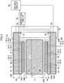
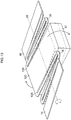
- Figure 1 is a perspective view of a MEMS scanner device according to a first embodiment.
- Figure 2 is an explanatory diagram that is a combination of a plan view (top view) of the MEMS scanner device according to the first embodiment as viewed from a reflection surface side of a mirror unit and a block configuration diagram showing circuit elements for device drive and angle detection.
- a MEMS scanner device 10 (corresponding to a “mirror driving device”) according to the embodiment includes a mirror unit 12, a pair of piezoelectric actuator units 14, 16 that are disposed at both sides of the mirror unit 12 so as to sandwich it, linking units 18, 20 that join one end portions 14A, 16A of the respective piezoelectric actuator units 14, 16 and end portions 12A, 12B of the mirror unit 12, and a fixing frame 30 (corresponding to a “fixing unit”) that fixedly supports the other end portions (hereinafter, referred to as base end portions) 14B, 16B of the piezoelectric actuator units 14, 16.
- the piezoelectric actuator unit of reference numeral 14 is referred to as the "first piezoelectric actuator unit”
- the piezoelectric actuator unit of reference numeral 16 is referred to as the "second piezoelectric actuator unit”.
- the linking unit of reference numeral 18 is referred to as the “first linking unit”
- the linking unit of reference numeral 20 is referred to as the "second linking unit”.
- the end portion of reference character 12A is referred to as the "first end portion”
- the end portion of reference character 12B is referred to as the "second end portion”.
- the mirror unit 12 has a roughly rectangular shape in planar view, and for increasing the reflectance of incident light, a metallic thin film of Au (gold), Al (aluminum) or the like is formed on a mirror surface (a top surface of the mirror unit 12), which is a reflection surface 12C to reflect light.
- the material to be used for the mirror coating and the film thickness are not particularly limited, and various designs are possible using a known mirror material (a high-reflectance material).
- the "rectangular shape" means a shape in which the whole of the basic shape can be roughly grasped as a rectangular shape. Examples thereof include a shape in which the corner portions of a rectangular shape are chamfered, a shape in which the corner portions are rounded off, a shape in which a part or whole of a side is configured by a curved line or a polygonal line, a shape in which an additional shape necessary for linking is added to the connecting parts between the mirror unit 12 and the respective linking units 18, 20, and the like.
- the shape of the mirror unit 12 is not particularly limited. Without being limited to an oblong shape exemplified in Figure 1 and Figure 2 , various shapes such as a square shape, a polygonal shape, a circular shape and an elliptical shape are possible. Further, the planar view shape of the mirror unit 12 and the shape of the reflection surface 12C may be coincide, or may be different. The reflection surface 12C can be formed within the area range of the top surface of the mirror unit 12.
- the embodiment exemplifies the mirror unit 12 having the reflection surface 12C with a roughly oblong shape in planar view, and, for explanation, applies orthogonal x, y and z axes in which the x-direction is defined as the long-side direction of the mirror unit 12 at the time of non-driving, the y-direction is defined as the short-side direction orthogonal to the y-direction, and the z-direction is defined as the direction perpendicular to the xy plane.
- the pair of piezoelectric actuator units 14, 16 are disposed so as to sandwich both sides in the y-axis direction of the mirror unit 12 in which the reflection surface 12C is oriented in the z-axis direction at the time of non-driving.
- the respective piezoelectric actuator units 14, 16 are actuators having a piezoelectric unimorph cantilever (cantilever beam) structure (see Figure 3 ), and perform bending displacement by the deformation of a piezoelectric substance due to the inverse piezoelectric effect.
- one end portions in the x-direction are fixedly supported by the fixing frame 30, and the end portions 14A, 16A on the opposite side, without being fixed by a frame or the like, are unconstraint ends that can be displaced because of the cantilever structure.
- the end portion 14A on the unconstraint side of the first piezoelectric actuator unit 14 is connected with one end portion 18A of the first linking unit 18, which is configured in a meandering form. Further, the other end portion 18B of the first linking unit 18 is connected with the first end portion 12A of a side along the x-axis direction of the mirror unit 12.
- the end portion 16A on the unconstraint side of the second piezoelectric actuator unit 16 is connected with one end portion 20A of the second linking unit 20, which is configured in a meandering form.
- the other end portion 20B of the second linking unit 20 is connected with the second end portion 12B in the x-axis direction of the mirror unit 12.
- the end portions (12A, 12B) in the x-axis direction of the mirror unit 12, with which the first linking unit 18 and the second linking unit 20 are connected respectively, are not required to be the farthest end positions in a strict sense, and include sites in ranges that are roughly grasped as end portions (at the farthest end positions and near the peripheries thereof).
- the MEMS scanner device 10 drives the first piezoelectric actuator unit 14 and the second piezoelectric actuator unit 16 to vibrate the x-axis-directional end portions (12A, 12B) of the mirror unit 12 up and down (in the thickness direction of the mirror unit 12), and thereby excites, to the mirror unit 12, the rotational resonance motion around a rotation axis 22 parallel to the y-axis, to perform the rotational drive of the mirror unit 12 (see Figure 4 ).
- the rotation axis 22 is a line that goes through a nearly central point of the reflection surface 12C and that is parallel to the y-axis.
- the first linking unit 18 and the second linking unit 20 are connected with sites that are near the peripheries of the end portions of the mirror unit 12 and that are away in the x-axis direction from the mirror center within ranges allowing for the achievement of such an intended resonant drive. That is, the first end portion 12A and second end portion 12B of the mirror unit 12 with which the first linking unit 18 and the second linking unit 20 are connected respectively are portions containing the ends of the mirror unit 12 away in the x-axis direction (in the direction perpendicular to the rotation axis 22) along the reflection surface 12C from the rotation axis 22 and the ranges around the vicinities of the ends.
- the first linking unit 18 and the second linking unit 20 have a structure in which multiple thin plate members 19 (corresponding to "plate-shaped members") having a flat-plate bar shape, whose longitudinal direction is the x-axis direction, are arrayed so as to be folded back in a meandering form.
- the embodiment exemplifies a structure in which two thin plate members 19 are arrayed in parallel and end portions of these two thin plate members 19 are connected with each other such that they are folded back in a meandering form.
- the number of the thin plate members 19 configuring each of the linking units (18, 20) is not particularly limited, and an appropriate number can be adopted if it is one or more.
- the first linking unit 18 and the second linking unit 20 each function as plate-shaped hinge units that deform the respective thin plate members 19 such that they are deflected (bent) in the thickness direction, by the drive of the first piezoelectric actuator unit 14 and the second piezoelectric actuator unit 16.
- the inertia force in the opposite direction to an acceleration direction (a direction in which force is applied) of the end portions 14A, 16A of the respective piezoelectric actuator units 14, 16 acts on the mirror unit 12.
- the inertia force matches a direction in which the mirror unit 12 is inclined, and therefore, the force generated in the piezoelectric actuator units 14, 16 is efficiently utilized as the force for inclining the mirror unit 12.
- the displacement direction of the piezoelectric actuator units 14, 16 roughly coincides with the rotation direction of the mirror unit 12 at all times and the whole force is used for the rotation of the mirror, the use efficiency of the force is much more excellent compared to the torsion bar structure. Further, even in the case of a large rotation angle, the energy loss is reduced, and therefore, a large displacement (inclination angle) can be obtained.
- linking units 18, 20 in a meandering form that join the mirror unit 12 and the piezoelectric actuator units 14, 16 accumulate the displacement by the gradual bending of the respective thin plate members 19, and therefore, have an advantage that the stress to be applied to the individual thin plate members 19 is reduced, and even in the case of a large rotation angle, they are hard to break.
- the multiple thin plate members 19 configuring the first linking unit 18 and the second linking unit 20 are referred to as the first thin plate member 19-1, the second thin plate member 19-2, the third thin plate member 19-3 and the fourth thin plate member 19-4, in the order from left to right in Figure 1 (from top to bottom in Figure 2 ).
- first linking unit 18 is configured such that the first thin plate member 19-1 and the second thin plate member 19-2 are joined.
- the second linking unit 20 is configured such that the third thin plate member 19-3 and the fourth thin plate member 19-4 are joined.
- the upper electrodes of the piezoelectric actuator units (14, 16) are referred to as the "drive electrodes”, and are designated by reference numerals 15 and 17.
- reference numerals 31, 32, 33 and 34 provided on the surface of the fixing frame 30 designate output terminals for detection signal output.
- the respective wires 51 to 54 are patterned on the piezoelectric substance film.
- the wire 51 which is led out of the detection electrode 25-1 formed on the top surface of the first thin plate member 19-1, is led, from the first thin plate member 19-1, around the proximity of the upper electrode (drive electrode 15) of the first piezoelectric actuator unit 14 along the longitudinal direction, to be joined to the output terminal (first output terminal) designated by reference numeral 31.
- the wire 52 which is led out of the detection electrode 25-2 formed on the top surface of the second thin plate member 19-2, is led around the proximity of the detection electrode 25-1 of the first thin plate member 19-1 along the longitudinal direction, and therewith, is led around the proximity of the upper electrode (drive electrode 15) of the first piezoelectric actuator unit 14 along the longitudinal direction, to be joined to the output terminal (second output terminal) designated by reference numeral 32.
- the wire 53 which is led out of the detection electrode 25-3 formed on the top surface of the third thin plate member 19-3, is led around the proximity of the detection electrode 25-4 of the fourth thin plate member 19-4 along the longitudinal direction, and therewith, is led around the proximity of the upper electrode (drive electrode 17) of the second piezoelectric actuator unit 16 along the longitudinal direction, to be joined to the output terminal (third output terminal) designated by reference numeral 33.
- the wire 54 which is led out of the detection electrode 25-4 formed on the fourth thin plate member 19-4, is led, from the fourth thin plate member 19-4, around the proximity of the upper electrode (drive electrode 17) of the second piezoelectric actuator unit 16 along the longitudinal direction, to be joined to the output terminal (fourth output terminal) designated by reference numeral 34.
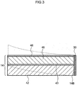
- FIG. 3 is a schematic diagram showing a cross-section structure of the piezoelectric actuator units 14, 16 having a piezoelectric unimorph cantilever structure.
- the piezoelectric actuator units 14, 16 have the same structure, and therefore, as a representative of them, the structure of the piezoelectric actuator unit of reference numeral 14 is described.
- a structure other than the unimorph cantilever may be used as the piezoelectric actuator unit.
- a bimorph cantilever in which two piezoelectric substance layers are laminated so as to sandwich electrodes may be used.
- the piezoelectric actuator unit 14 has a structure in which a lower electrode 43, a piezoelectric substance 46 and an upper electrode 48 are laminated and formed on a vibration plate 42.
- a laminate structure body can be obtained, for example, by sequentially forming the respective layers of the lower electrode 43, piezoelectric substance 46 and upper electrode 48 on a silicon (Si) substrate.
- the right end in Figure 3 is the fixed end that is supported by the fixing frame 30 (see Figure 1 and Figure 2 ).
- a drive voltage is applied between the electrodes (43, 48), and thereby, the piezoelectric substance 46 is deformed.
- the vibration plate 42 is deflected, and the lever unit moves up and down.
- the broken line in Figure 3 shows a manner in which the lever unit is displaced upward.
- the piezoelectric actuator units 14, 16 are means for converting an electric signal into a mechanical displacement by utilizing the inverse piezoelectric effect of the piezoelectric substance 46.
- the driving circuit 62 applies the same drive voltage to the pair of piezoelectric actuator units 14, 16 simultaneously, and thereby, the piezoelectric actuator units 14, 16 at both sides of the mirror unit 12 are displaced in the same direction. Therefore, as a power supply source to supply the power for drive to the pair of piezoelectric actuator units 14, 16, the common (same) driving circuit 62 can be used.
- the drive waveform to be supplied to the piezoelectric actuator units 14, 16 a sinusoidal waveform signal or pulse waveform signal that has a frequency for exciting the resonance can be used.
- the MEMS scanner device 10 acts as follows.
- the piezoelectric actuator units 14, 16 When the driving circuit 62 applies the same drive voltage to the pair of piezoelectric actuator units 14, 16 simultaneously, the piezoelectric actuator units 14, 16 are displaced, and the linking units 18, 20 in a meandering form that are connected with them are bent and deformed. Then, the end portions 12A, 12B of the mirror unit 12 that are connected with the linking units 18, 20 are displaced in the vertical direction (z-axis direction). By this action, the rotational torque is given to the mirror unit 12, and the mirror unit 12 performs the rotational motion around the rotation axis 22.
- the piezoelectric actuator units 14, 16 are vibrated up and down, and the rotational motion of the mirror unit 12 is induced.
- the resonant drive is performed by the application of a drive voltage having a frequency near the resonant frequency, the mirror unit 12 vibrates at a large inclination angle.
- the linking units 18, 20 in a meandering form are easily bent and deformed, and therefore, are effective in obtaining a large displacement in the resonant drive (see Figure 4 and Figure 5 ).
- the frequency of the drive voltage to be applied to the piezoelectric actuator units 14, 16 is not necessarily required to strictly coincide with the mechanical resonant frequency of the structure body. The difference in the frequency of the drive voltage is allowable in a range in which the resonance is excited.
- the rotational resonance motion enables the mirror unit 12 to be displaced around the rotation axis 22 at a large rotation angle. That is, in response to the drive of the piezoelectric actuator units 14, 16, the mirror unit 12 at the middle swings around the rotation axis 22.
- the light for example, the laser beam emitted from a laser beam source not shown in the figure
- the MEMS scanner device 10 can perform light scanning at a large deflection angle.
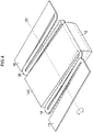
- Figure 4 and Figure 5 are explanatory diagrams for explaining the stress (pxx component) to be applied to the linking units (plate-shaped hinge units) during the resonant drive.
- Figure 4 is a perspective view showing a manner at the time of driving in a rotation resonance mode.
- Figure 5 is a schematic diagram of the first linking unit 18 shown in Figure 4 , as viewed from the positive direction of the y-axis.
- the description of the fixing frame 30 is omitted.
- the action of the second linking unit 20 is the same as the action of the first linking unit 18.
- the thin plate members 19-1, 19-2 configuring the first linking unit 18 are deformed so as to be deflected in opposite directions to each other, and stresses in opposite directions to each other are applied to the surfaces of the respective thin plate members 19-1, 19-2. That is, as shown in Figure 5 , when the first thin plate member 19-1 performs such an action (bending deformation) that it becomes convex downward, the second thin plate member 19-2 performs such an action that it becomes convex upward. On this occasion, a compressive stress is applied to the surface of the first thin plate member 19-1, and a tensile stress is applied to the surface of the second thin plate member 19-2.
- first thin plate member 19-1 (hinge 1) and second thin plate member 19-2 (hinge 2) are deflected in the opposite directions to each other, and an angle displacement ⁇ 1 due to the bending of the first thin plate member 19-1 and an angle displacement ⁇ 2 due to the bending of the second thin plate member 19-2 are added to give the inclination angle of the mirror unit 12.
- the reflection surface 12C of the mirror unit 12 is inclined around the y-axis at an angle of ( ⁇ 1 + ⁇ 2).
- the stresses applied to the first thin plate member 19-1 and the second thin plate member 19-2 are detected as the voltages between the upper electrodes and lower electrodes of the sensor units 24-1, 24-2, and thereby, they function as angle sensors.
- the structure according to the embodiment allows for an angle detection that is excellent in linearity. Further, an AGC (Automatic Gain Control) circuit and a phase synchronization (PLL; Phase-Locked Loop) circuit are built, and using the angle detection signal acquired in that way, the feedback is performed to the voltage to be applied to the piezoelectric actuator units. Thereby, even when the resonant frequency is changed by a change in environmental temperature or the like, it is possible to keep the scan angle constant. For example, the feedback is performed to the driving circuit, such that the waveforms applied to the piezoelectric actuator units and the phases of the waveforms detected by the sensor units have predetermined values, and thereby, the resonance is maintained.
- AGC Automatic Gain Control
- PLL Phase-Locked Loop
- Such a feedback control circuit can be embedded in the detecting circuit 64. Further, the driving circuit 62, the detecting circuit 64 and the feedback control circuit can be collectively configured as an integrated circuit such as an ASIC (Application Specific Integrated Circuit).
- ASIC Application Specific Integrated Circuit
- the sensor unit only needs to be provided on a part of the thin plate member 19, within a range allowing for the achievement of the intended function by which the stress of the thin plate member 19 is detected, and the detection electrode having an appropriate size can be designed.
- piezoelectric substance suitable for the embodiment there is a piezoelectric substance containing one kind of, or two or more kinds of perovskite-type oxides (P) that are represented by the following formula.
- P perovskite-type oxides
- Examples of the perovskite-type oxide to be represented by the above general formula include lead-containing compounds such as lead titanate, lead zirconate titanate (PZT), lead zirconate, lead lanthanum titanate, lead lanthanum zirconate titanate, lead magnesium niobate zirconium titanate, lead nickel niobate zirconium titanate, and lead zinc niobate zirconium titanate, and a mixed crystal system of them; and non-lead-containing compound such as barium titanate, barium strontium titanate, bismuth sodium titanate, bismuth potassium titanate, sodium niobate, potassium niobate, lithium niobate, and bismuth ferrite, and a mixed crystal system of them.
- lead-containing compounds such as lead titanate, lead zirconate titanate (PZT), lead zirconate, lead lanthanum titanate, lead lanthanum zirconate titanate, lead magnesium
- the piezoelectric substance film according to the embodiment contain one kind of, or two or more kinds of perovskite-type oxides (PX) that are represented by the following formula.
- PX perovskite-type oxides
- the perovskite-type oxide (PX) is intrinsic PZT, or a PZT in which M is substituted for a part of the B-sites. It is known that, in a PZT to which various kinds of donor ions having a higher valence than the valence of the substitution-target ion have been added, properties such as piezoelectric performance are improved relative to intrinsic PZT. It is preferable that M is one kind of, or two or more kinds of donor ions that have a higher valence than quadrivalent Zr and Ti. Examples of such a donor ion include V 5+ , Nb 5+ , Ta 5+ , Sb 5+ , Mo 6+ , and W 6+ , and the like.
- b - x - y is not particularly limited.
- the molar ratio of Nb / (Zr + Ti + Nb) preferably, should be 0.05 or more and 0.25 or less, and more preferably, should be 0.06 or more and 0.20 or less.
- a piezoelectric substance film composed of the perovskite-type oxide represented by the above-described General Formulas (P) and (PX) has a high piezoelectric distortion constant (d31 constant), and therefore, a piezoelectric actuator including such a piezoelectric substance film is excellent in displacement property.
- the piezoelectric actuator including the piezoelectric substance film composed of the perovskite-type oxide represented by General Formulas (P) and (PX) has a voltage-displacement property that is excellent in linearity. These piezoelectric materials exhibit a good actuator property and sensor property, in the practice of the present invention.
- the perovskite-type oxide represented by General Formula (PX) has a higher piezoelectric constant than that represented by General Formula (P).
- a lead zirconate titanate (PZT) thin film in which 12% Nb in atomic composition percentage has been doped can be used, for example.
- a piezoelectric substance in bulk may be jointed on a substrate and may be polished, but in that method, it is difficult to perform the thinning of the piezoelectric substance (in polishing, the limit is about 15 ⁇ m).
- the piezoelectric thin film is directly formed on the substrate by a vapor growth method, a sol-gel method or the like.
- the piezoelectric substance 46 according to the embodiment is a thin film having a thickness of 1 ⁇ m or more and 10 ⁇ m or less.
- a vapor growth method is preferable.
- various methods such as an ion plating method, a MOCVD method (metal organic chemical vapor growth method) and a PLD method (pulsed laser deposition method) can be applied.
- a method for example, a sol-gel method
- a sol-gel method other than the vapor growth method may be considered.
- Example 1 described later as the piezoelectric substance 46, a PZT thin film that is formed by a sputtering method and that has a thickness of 4 ⁇ m is used, but the piezoelectric substance 46 is not limited to this.
- the MEMS scanner device 10 was made in the following procedure.
- the fixing frame 30 has a structure in which both the handle layer and the device layer are utilized, and the thickness is about 360 ⁇ m.
- the piezoelectric actuator unit and the plate-shaped hinge unit both have a laminate structure of the Si device layer (10 ⁇ m), the lower electrode, the PZT thin film and the upper electrode.
- the piezoelectric actuator unit functions as a piezoelectric thin film unimorph actuator that is deformed so as to be deflected up and down by the application of a voltage between the upper and lower electrodes.
- the piezoelectric actuator units 14, 16 have a laminate structure of the Si device layer (10 ⁇ m), the lower electrode, the PZT thin film and the upper electrode, and functions as a piezoelectric thin film unimorph actuator.
- Example 1 the PZT thin film is formed by being directly formed on the substrate by the sputtering method and thereafter being processed by the dry etching.
- the configuration in the practice of the present invention is not limited to the thin film piezoelectric substance.
- a bulk piezoelectric substance may be bonded to a vibration plate, and thereby a unimorph actuator may be formed.
- two piezoelectric substances having different polarities may be bonded, and thereby a bimorph actuator may be formed.
- the substrate material, the electrode material, the piezoelectric material, the film thickness, the film formation condition and the like can be appropriately selected depending on the purpose.
- Vsense1 shows the signals from the detection electrodes 25-1, 25-4
- Vsense2 shows the signals from the detection electrodes 25-2, 25-3.
- Figure 7 shows plots of the relation between the scan angle and the detection voltage when the drive voltage to be given to the piezoelectric actuator units 14, 16 was changed.
- “Differential” shows the differential between the two voltage signals (Vsense1, Vsense2) that was detected by a differential circuit.
- the angle detectability of each detection electrode was as follows.
- the differential circuit is embedded in the detecting circuit 64 shown in Figure 2 .
- the MEMS scanner device 10 shown in Figure 1 has a bilaterally symmetric structure across the mirror unit 12.
- the first thin plate member 19-1 and the fourth thin plate member 19-24 perform an equivalent action
- the second thin plate member 19-2 and the third thin plate member 19-3 perform an equivalent action.
- a similar detection signal (Vsense1 in Figure 6 ) is obtained.
- a similar detection signal (Vsense2 in Figure 6 ) is obtained.
- the combination of the first thin plate member 19-1 and the third thin plate member 19-3, the combination of the second thin plate member 19-2 and the fourth thin plate member 19-4, and the combination of the third thin plate member 19-3 and the fourth thin plate member 19-4 are also possible, in addition to the combination of the first thin plate member 19-1 and the second thin plate member 19-2, and any combination may be adopted.
- the number of the thin plate members configuring the linking units (18, 20) in a meandering form is generalized to be m (m is an integer of 2 or more).
- m is an integer of 2 or more.
- the initial value of the consecutive numbers j is not limited to "1", but may be "0", and an arbitrary integer can be adopted.
- the sensor unit it is not necessarily required to provide the sensor unit for all the thin plate members 19-1 to 19-4, and a configuration in which a sensor unit not to be used for sensing is omitted is also possible.
- Example 2 a MEMS scanner device having the same structure as Example 1 was made by the same making method as Example 1, except that a material having a composition of Pb 1.3 (Zr 0.52 Ti 0.48 )O 3 was used as the target material in the PZT film formation.
- a material having a composition of Pb 1.3 (Zr 0.52 Ti 0.48 )O 3 was used as the target material in the PZT film formation.
- Figure 8 shows a relation between applied voltages and optical scan angles. Figure 8 concurrently describes the result of Example 1 (Nb 12% PZT).
- the white triangle marks show the measurement results when a polarization process was not performed for a PZT in which Nb had not been doped.
- the black triangle marks show the measurement results when a polarization process was performed after the film formation for the PZT in which Nb had not been doped.
- the black circle marks show the measurement results of Example 1 using the PZT (with no polarization process) in which 12% Nb had been doped.
- Figure 9 shows a chart in which relations between Nb doping amounts in a PZT and actuator properties/sensing properties are arranged.
- values when the polarization was not performed are used.
- the decision of whether the polarization process is necessary in the case where the scan angle in the non-polarized state (when 0.5 Vpp was applied) was less than or equal to 0.8 fold of the scan angle after the polarization process, a decision of "C" (the polarization process is necessary) was made. In the case of being more than 0.8 fold and less than or equal to 0.9 fold, a decision of "A" (the use is possible with no polarization process) was made. In the case of being more than 0.9 fold, a decision of "AA” (the polarization process is unnecessary) was made.
- the piezoelectric property increases with the increase in the Nb doping amount. Therefore, a more Nb doping amount can give a high scan angle at a lower voltage, and give a higher detection voltage in the angle detection.
- the first embodiment, and Examples 1 and 2 use the structure in which the piezoelectric substance thin film is laminated on the linking units 18, 20 functioning as the plate-shaped hinge units, and the stresses are converted into voltages by the piezoelectric effect.
- the means for detecting the stress in the plate-shaped hinge unit is not limited to this example.
- the means for detecting the stress to be generated in the linking unit a mode in which the piezo-resistance effect is utilized is also possible.
- a configuration in which boron doping is performed to the surfaces of the linking units 18, 20 of silicon (Si), a p-type Si layer exhibiting the piezo-resistance effect is formed, and the stress detection is performed by utilizing the change in the electric resistance of the p-type Si layer due to the applied stress may be employed.
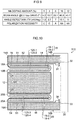
- FIG 10 is a plan view showing the configuration of a MEMS scanner device according to a second embodiment.
- the linking units 18, 20 are configured by a p-type Si in which boron is diffused on a part of the Si surface, and the stress is detected by utilizing a piezo-resistance effect by which the electric resistance of the p-type Si part changes due to the stress to be applied to the linking units 18, 20.
- the change in the resistance value with use of a circuit to convert it into a voltage, is detected as a voltage signal.
- Figure 11 is a configuration diagram of a circuit to convert a change in the resistance value into a voltage.
- the R1 and R2 in the figure show the resistances of piezo-resistance material units provided on thin plate members that are displaced in opposite directions to each other, respectively. That is, the R1 shows the resistance of a piezo-resistance material unit provided on an odd-numbered thin plate member (for example, the resistance of the piezo-resistance material unit 125-3 provided on the third thin plate member 19-3), and the R2 shows the resistance of a piezo-resistance material unit provided on an even-numbered thin plate member (for example, the resistance of the piezo-resistance material unit 125-4 provided on the fourth thin plate member 19-4).
- a voltage dividing circuit connecting the R1 and the R2 is configured, and a voltage signal Vout after the division by the R1 and the R2 is obtained.
- a circuit is embedded in the detecting circuit 64.
- the actuator unit and the sensor unit can be formed simultaneously in the same process, allowing for the simplification of the process and the reduction of the cost.
- the configuration of the detecting circuit is also simple.
- Figure 12 is a plan view of a principal part of a MEMS scanner device 210 according to a third embodiment
- Figure 13 is a perspective view showing an action state in the rotation resonance mode.
- the linking units 18, 20 functioning as the plate-shaped hinge units have a structure in which three thin plate members are joined in a meandering form.
- the other configuration is the same configuration as the first embodiment. Since the number of thin plate members is increased, it is possible to obtain a lower resonant frequency than the first embodiment.
- the linking unit 18 shown in Figure 12 has a structure in which thin plate members 219-1, 219-2, 219-3 are arrayed so as to be folded back in a meandering form. Further, the linking unit 20 has a structure in which thin plate members 219-4, 219-5, 219-6 are arrayed so as to be folded back in a meandering form.
- detection electrodes 225-3, 225-4 are provided on the odd-numbered thin plate members 219-3, 219-4 with respect to the sides close to the mirror unit 12, and detection electrodes 225-2, 225-5 are provided on the even-numbered thin plate members 219-2, 219-5.
- the illustration of the wires (51 to 54) and output terminals (31 to 34) is omitted.
- the thin plate members designated by reference numerals 219-1, 219-6 fall under "odd-numbered", and therefore, a mode in which detection electrodes are provided on the thin plate members 219-1, 219-6 instead of the detection electrodes 225-3, 225-4 or along with them is also possible.
- the end portions 12A, 12B of the mirror unit 12 are vibrated up and down by the vertical drive of the piezoelectric actuator units 14, 16, and thereby, the inclining (rotational) motion of the mirror unit 12 is induced by the inertia force, and the mirror unit 12 is largely inclined by the resonant vibration (see Figure 13 ).
- the linking units having a tortuous shape (the plate-shaped hinge units folded back in a meandering form) 18, 20 are provided between the mirror unit 12 and the piezoelectric actuator units 14, 16, and thereby, the displacement of the inclination angle of the mirror unit 12 is further enlarged. Then, it is possible to detect the stresses to be generated in the linking units during the rotational drive, and to grasp the angle of the mirror unit 12.
- the tortuous shape (meandering form) of the linking unit is not an indispensable element, and a mode in which the linking unit is configured by one thin plate member functioning as the plate-shaped hinge is also possible.
- PZT piezoelectric material to be used for the piezoelectric actuator unit and the sensor unit
- PZT piezoelectric material to be used for the piezoelectric actuator unit and the sensor unit
- a non-lead piezoelectric substance such as BaTiO 3 , KNaNbO 3 and BiFeO 3
- a non-perovskite piezoelectric substance such as AIN and ZnO 2 can be used.
- a piezoelectric actuator unit in which multiple piezoelectric cantilevers are combined can be employed.
- a piezoelectric cantilever having a folding structure in a meandering form can be employed.
- whether the folding structure of the cantilever unit is employed, and the number of times of folding (the number of folds) are not particularly limited. It is possible to increase the displacement amount with the increase in the number of folds of the cantilever.
- the resonant frequency tends to be decreased as the number of folds is increased. Further, the resonant frequency tends to be decreased as the width of the lever unit or plate-shaped member (hinge plate) is thinned.
- the present invention can be utilized for various uses, as an optical device that reflects light such as laser beam and changes the advancing direction of the light.
- the present invention can be widely applied to an optical deflector, an optical scanner, a laser printer, a bar code reader, a display device, various optical sensors (a distance measuring sensor, a shape measuring sensor), an optical communication device, a laser projector, an OCT image diagnosis device, and the like.
Applications Claiming Priority (2)
| Application Number | Priority Date | Filing Date | Title |
|---|---|---|---|
| JP2012212238A JP5916577B2 (ja) | 2012-09-26 | 2012-09-26 | ミラー駆動装置及びその駆動方法 |
| PCT/JP2013/074648 WO2014050586A1 (ja) | 2012-09-26 | 2013-09-12 | ミラー駆動装置及びその駆動方法 |
Publications (3)
| Publication Number | Publication Date |
|---|---|
| EP2902836A1 EP2902836A1 (en) | 2015-08-05 |
| EP2902836A4 EP2902836A4 (en) | 2016-05-04 |
| EP2902836B1 true EP2902836B1 (en) | 2021-10-27 |
Family
ID=50387993
Family Applications (1)
| Application Number | Title | Priority Date | Filing Date |
|---|---|---|---|
| EP13841383.6A Active EP2902836B1 (en) | 2012-09-26 | 2013-09-12 | Mirror driving device and driving method for same |
Country Status (4)
| Country | Link |
|---|---|
| US (1) | US10048489B2 (ja) |
| EP (1) | EP2902836B1 (ja) |
| JP (1) | JP5916577B2 (ja) |
| WO (1) | WO2014050586A1 (ja) |
Families Citing this family (22)
| Publication number | Priority date | Publication date | Assignee | Title |
|---|---|---|---|---|
| US10739460B2 (en) | 2010-08-11 | 2020-08-11 | Apple Inc. | Time-of-flight detector with single-axis scan |
| JP5654158B1 (ja) * | 2014-05-07 | 2015-01-14 | 株式会社トライフォース・マネジメント | 可動反射素子および二次元走査装置 |
| US9624100B2 (en) | 2014-06-12 | 2017-04-18 | Apple Inc. | Micro pick up array pivot mount with integrated strain sensing elements |
| DE102014217799B4 (de) * | 2014-09-05 | 2019-11-21 | Fraunhofer-Gesellschaft zur Förderung der angewandten Forschung e.V. | Piezoelektrischer Positionssensor für piezoelektrisch angetriebene resonante Mikrospiegel |
| US9705432B2 (en) * | 2014-09-30 | 2017-07-11 | Apple Inc. | Micro pick up array pivot mount design for strain amplification |
| JP6606865B2 (ja) * | 2015-05-29 | 2019-11-20 | ミツミ電機株式会社 | 光走査装置及びその製造方法、光走査制御装置 |
| JP6498047B2 (ja) | 2015-06-09 | 2019-04-10 | 株式会社トライフォース・マネジメント | 可動反射装置およびこれを利用した反射面駆動システム |
| CN104977104B (zh) * | 2015-07-13 | 2017-04-12 | 大连理工大学 | 一种压电式小量程大量程比的测力装置 |
| US10298913B2 (en) * | 2016-08-18 | 2019-05-21 | Apple Inc. | Standalone depth camera |
| IT201600132144A1 (it) * | 2016-12-29 | 2018-06-29 | St Microelectronics Srl | Dispositivo attuatore micro-elettro-meccanico con comando piezoelettrico, mobile nel piano |
| JP6354892B2 (ja) * | 2017-05-18 | 2018-07-11 | 株式会社リコー | 位置検出装置と映像機器 |
| WO2019021400A1 (ja) * | 2017-07-26 | 2019-01-31 | 株式会社 トライフォース・マネジメント | 発電素子 |
| DE102017220813A1 (de) * | 2017-11-22 | 2019-05-23 | Robert Bosch Gmbh | Laserprojektionsvorrichtung |
| JP6985602B2 (ja) * | 2018-01-29 | 2021-12-22 | ミツミ電機株式会社 | 光走査装置及び光走査装置の製造方法 |
| IT201800002364A1 (it) | 2018-02-02 | 2019-08-02 | St Microelectronics Srl | Dispositivo micro-manipolatore micro-elettro-meccanico con comando piezoelettrico, mobile nel piano |
| DE102018215528A1 (de) * | 2018-09-12 | 2020-03-12 | Robert Bosch Gmbh | Mikromechanisches Bauteil und Herstellungsverfahren für ein mikromechanisches Bauteil |
| US11221478B2 (en) * | 2019-04-15 | 2022-01-11 | Microsoft Technology Licensing, Llc | MEMS scanner |
| US11175492B2 (en) | 2019-08-12 | 2021-11-16 | Microsoft Technology Licensing, Llc | Substrate for scanning mirror system |
| US11750779B2 (en) | 2019-08-20 | 2023-09-05 | Ricoh Company, Ltd. | Light deflector, optical scanning system, image projection device, image forming apparatus, and lidar device |
| CN112752209B (zh) * | 2019-10-31 | 2022-03-25 | 华为技术有限公司 | 一种压电式mems传感器以及相关设备 |
| CN111289155B (zh) * | 2020-02-26 | 2021-07-13 | 西安交通大学 | 基于电磁激励压阻检测的面内振动硅微谐振式压力传感器 |
| US20220026537A1 (en) * | 2020-07-22 | 2022-01-27 | Beijing Voyager Technology Co., Ltd. | Systems and methods for sensing rotation angles of a micro mirror in an optical sensing system |
Family Cites Families (10)
| Publication number | Priority date | Publication date | Assignee | Title |
|---|---|---|---|---|
| JP2008039810A (ja) * | 2006-08-01 | 2008-02-21 | Matsushita Electric Ind Co Ltd | 光学反射素子 |
| JP4926596B2 (ja) | 2006-08-08 | 2012-05-09 | スタンレー電気株式会社 | 光偏向器及びその製造方法 |
| DE102007058239B4 (de) * | 2007-12-04 | 2021-04-29 | Robert Bosch Gmbh | Mikrospiegelvorrichtung |
| JP2009258210A (ja) * | 2008-04-14 | 2009-11-05 | Panasonic Corp | 光学反射素子 |
| AU2009266808B2 (en) * | 2008-07-03 | 2014-07-10 | Teleflex Life Sciences Limited | Apparatus and methods for treating obstructions within body lumens |
| KR101287267B1 (ko) * | 2009-05-11 | 2013-07-17 | 파나소닉 주식회사 | 광학 반사 소자 |
| JP2011095523A (ja) * | 2009-10-30 | 2011-05-12 | Panasonic Corp | 光学反射素子 |
| JP5400636B2 (ja) | 2010-01-20 | 2014-01-29 | スタンレー電気株式会社 | 光偏向器及びこれを用いた光学装置 |
| JP5293668B2 (ja) * | 2010-03-30 | 2013-09-18 | パナソニック株式会社 | 光学反射素子 |
| JP5592192B2 (ja) * | 2010-08-11 | 2014-09-17 | 富士フイルム株式会社 | 圧電体膜とその製造方法、圧電素子および液体吐出装置 |
-
2012
- 2012-09-26 JP JP2012212238A patent/JP5916577B2/ja active Active
-
2013
- 2013-09-12 EP EP13841383.6A patent/EP2902836B1/en active Active
- 2013-09-12 WO PCT/JP2013/074648 patent/WO2014050586A1/ja active Application Filing
-
2015
- 2015-03-25 US US14/668,429 patent/US10048489B2/en active Active
Non-Patent Citations (1)
| Title |
|---|
| None * |
Also Published As
| Publication number | Publication date |
|---|---|
| WO2014050586A1 (ja) | 2014-04-03 |
| EP2902836A4 (en) | 2016-05-04 |
| JP2014066876A (ja) | 2014-04-17 |
| US20150198801A1 (en) | 2015-07-16 |
| JP5916577B2 (ja) | 2016-05-11 |
| EP2902836A1 (en) | 2015-08-05 |
| US10048489B2 (en) | 2018-08-14 |
Similar Documents
| Publication | Publication Date | Title |
|---|---|---|
| EP2902836B1 (en) | Mirror driving device and driving method for same | |
| US9864189B2 (en) | Mirror drive device and driving method thereof | |
| EP2827183B1 (en) | Mirror drive device and driving method thereof | |
| US8879132B2 (en) | Mirror driving apparatus, method of driving same and method of manufacturing same | |
| US9030721B2 (en) | Mirror driving device and method of controlling the device | |
| EP3203297B1 (en) | Mirror drive device and drive method therefor | |
| JP5264954B2 (ja) | ミラー駆動装置及び方法 | |
| EP3203298B1 (en) | Mirror drive device and drive method therefor | |
| US20210223539A1 (en) | Micromirror device and method of driving micromirror device | |
| JP5344110B1 (ja) | 圧電体膜、インクジェットヘッド、インクジェットヘッドを用いて画像を形成する方法、角速度センサ、角速度センサを用いて角速度を測定する方法、圧電発電素子ならびに圧電発電素子を用いた発電方法 |
Legal Events
| Date | Code | Title | Description |
|---|---|---|---|
| PUAI | Public reference made under article 153(3) epc to a published international application that has entered the european phase |
Free format text: ORIGINAL CODE: 0009012 |
|
| 17P | Request for examination filed |
Effective date: 20150325 |
|
| AK | Designated contracting states |
Kind code of ref document: A1 Designated state(s): AL AT BE BG CH CY CZ DE DK EE ES FI FR GB GR HR HU IE IS IT LI LT LU LV MC MK MT NL NO PL PT RO RS SE SI SK SM TR |
|
| AX | Request for extension of the european patent |
Extension state: BA ME |
|
| DAX | Request for extension of the european patent (deleted) | ||
| RA4 | Supplementary search report drawn up and despatched (corrected) |
Effective date: 20160406 |
|
| RIC1 | Information provided on ipc code assigned before grant |
Ipc: H01L 41/09 20060101ALI20160331BHEP Ipc: G02B 26/08 20060101ALI20160331BHEP Ipc: G02B 26/10 20060101AFI20160331BHEP Ipc: B81B 3/00 20060101ALI20160331BHEP Ipc: H01L 41/187 20060101ALI20160331BHEP |
|
| STAA | Information on the status of an ep patent application or granted ep patent |
Free format text: STATUS: EXAMINATION IS IN PROGRESS |
|
| 17Q | First examination report despatched |
Effective date: 20190219 |
|
| STAA | Information on the status of an ep patent application or granted ep patent |
Free format text: STATUS: EXAMINATION IS IN PROGRESS |
|
| RAP3 | Party data changed (applicant data changed or rights of an application transferred) |
Owner name: FUJIFILM CORPORATION |
|
| GRAP | Despatch of communication of intention to grant a patent |
Free format text: ORIGINAL CODE: EPIDOSNIGR1 |
|
| STAA | Information on the status of an ep patent application or granted ep patent |
Free format text: STATUS: GRANT OF PATENT IS INTENDED |
|
| INTG | Intention to grant announced |
Effective date: 20210629 |
|
| GRAS | Grant fee paid |
Free format text: ORIGINAL CODE: EPIDOSNIGR3 |
|
| GRAA | (expected) grant |
Free format text: ORIGINAL CODE: 0009210 |
|
| STAA | Information on the status of an ep patent application or granted ep patent |
Free format text: STATUS: THE PATENT HAS BEEN GRANTED |
|
| AK | Designated contracting states |
Kind code of ref document: B1 Designated state(s): AL AT BE BG CH CY CZ DE DK EE ES FI FR GB GR HR HU IE IS IT LI LT LU LV MC MK MT NL NO PL PT RO RS SE SI SK SM TR |
|
| REG | Reference to a national code |
Ref country code: GB Ref legal event code: FG4D |
|
| REG | Reference to a national code |
Ref country code: CH Ref legal event code: EP |
|
| REG | Reference to a national code |
Ref country code: AT Ref legal event code: REF Ref document number: 1442297 Country of ref document: AT Kind code of ref document: T Effective date: 20211115 |
|
| REG | Reference to a national code |
Ref country code: DE Ref legal event code: R096 Ref document number: 602013079830 Country of ref document: DE |
|
| REG | Reference to a national code |
Ref country code: IE Ref legal event code: FG4D |
|
| REG | Reference to a national code |
Ref country code: LT Ref legal event code: MG9D |
|
| REG | Reference to a national code |
Ref country code: NL Ref legal event code: MP Effective date: 20211027 |
|
| REG | Reference to a national code |
Ref country code: AT Ref legal event code: MK05 Ref document number: 1442297 Country of ref document: AT Kind code of ref document: T Effective date: 20211027 |
|
| PG25 | Lapsed in a contracting state [announced via postgrant information from national office to epo] |
Ref country code: RS Free format text: LAPSE BECAUSE OF FAILURE TO SUBMIT A TRANSLATION OF THE DESCRIPTION OR TO PAY THE FEE WITHIN THE PRESCRIBED TIME-LIMIT Effective date: 20211027 Ref country code: LT Free format text: LAPSE BECAUSE OF FAILURE TO SUBMIT A TRANSLATION OF THE DESCRIPTION OR TO PAY THE FEE WITHIN THE PRESCRIBED TIME-LIMIT Effective date: 20211027 Ref country code: FI Free format text: LAPSE BECAUSE OF FAILURE TO SUBMIT A TRANSLATION OF THE DESCRIPTION OR TO PAY THE FEE WITHIN THE PRESCRIBED TIME-LIMIT Effective date: 20211027 Ref country code: BG Free format text: LAPSE BECAUSE OF FAILURE TO SUBMIT A TRANSLATION OF THE DESCRIPTION OR TO PAY THE FEE WITHIN THE PRESCRIBED TIME-LIMIT Effective date: 20220127 Ref country code: AT Free format text: LAPSE BECAUSE OF FAILURE TO SUBMIT A TRANSLATION OF THE DESCRIPTION OR TO PAY THE FEE WITHIN THE PRESCRIBED TIME-LIMIT Effective date: 20211027 |
|
| PG25 | Lapsed in a contracting state [announced via postgrant information from national office to epo] |
Ref country code: IS Free format text: LAPSE BECAUSE OF FAILURE TO SUBMIT A TRANSLATION OF THE DESCRIPTION OR TO PAY THE FEE WITHIN THE PRESCRIBED TIME-LIMIT Effective date: 20220227 Ref country code: SE Free format text: LAPSE BECAUSE OF FAILURE TO SUBMIT A TRANSLATION OF THE DESCRIPTION OR TO PAY THE FEE WITHIN THE PRESCRIBED TIME-LIMIT Effective date: 20211027 Ref country code: PT Free format text: LAPSE BECAUSE OF FAILURE TO SUBMIT A TRANSLATION OF THE DESCRIPTION OR TO PAY THE FEE WITHIN THE PRESCRIBED TIME-LIMIT Effective date: 20220228 Ref country code: PL Free format text: LAPSE BECAUSE OF FAILURE TO SUBMIT A TRANSLATION OF THE DESCRIPTION OR TO PAY THE FEE WITHIN THE PRESCRIBED TIME-LIMIT Effective date: 20211027 Ref country code: NO Free format text: LAPSE BECAUSE OF FAILURE TO SUBMIT A TRANSLATION OF THE DESCRIPTION OR TO PAY THE FEE WITHIN THE PRESCRIBED TIME-LIMIT Effective date: 20220127 Ref country code: NL Free format text: LAPSE BECAUSE OF FAILURE TO SUBMIT A TRANSLATION OF THE DESCRIPTION OR TO PAY THE FEE WITHIN THE PRESCRIBED TIME-LIMIT Effective date: 20211027 Ref country code: LV Free format text: LAPSE BECAUSE OF FAILURE TO SUBMIT A TRANSLATION OF THE DESCRIPTION OR TO PAY THE FEE WITHIN THE PRESCRIBED TIME-LIMIT Effective date: 20211027 Ref country code: HR Free format text: LAPSE BECAUSE OF FAILURE TO SUBMIT A TRANSLATION OF THE DESCRIPTION OR TO PAY THE FEE WITHIN THE PRESCRIBED TIME-LIMIT Effective date: 20211027 Ref country code: GR Free format text: LAPSE BECAUSE OF FAILURE TO SUBMIT A TRANSLATION OF THE DESCRIPTION OR TO PAY THE FEE WITHIN THE PRESCRIBED TIME-LIMIT Effective date: 20220128 Ref country code: ES Free format text: LAPSE BECAUSE OF FAILURE TO SUBMIT A TRANSLATION OF THE DESCRIPTION OR TO PAY THE FEE WITHIN THE PRESCRIBED TIME-LIMIT Effective date: 20211027 |
|
| REG | Reference to a national code |
Ref country code: DE Ref legal event code: R097 Ref document number: 602013079830 Country of ref document: DE |
|
| PG25 | Lapsed in a contracting state [announced via postgrant information from national office to epo] |
Ref country code: SM Free format text: LAPSE BECAUSE OF FAILURE TO SUBMIT A TRANSLATION OF THE DESCRIPTION OR TO PAY THE FEE WITHIN THE PRESCRIBED TIME-LIMIT Effective date: 20211027 Ref country code: SK Free format text: LAPSE BECAUSE OF FAILURE TO SUBMIT A TRANSLATION OF THE DESCRIPTION OR TO PAY THE FEE WITHIN THE PRESCRIBED TIME-LIMIT Effective date: 20211027 Ref country code: RO Free format text: LAPSE BECAUSE OF FAILURE TO SUBMIT A TRANSLATION OF THE DESCRIPTION OR TO PAY THE FEE WITHIN THE PRESCRIBED TIME-LIMIT Effective date: 20211027 Ref country code: EE Free format text: LAPSE BECAUSE OF FAILURE TO SUBMIT A TRANSLATION OF THE DESCRIPTION OR TO PAY THE FEE WITHIN THE PRESCRIBED TIME-LIMIT Effective date: 20211027 Ref country code: DK Free format text: LAPSE BECAUSE OF FAILURE TO SUBMIT A TRANSLATION OF THE DESCRIPTION OR TO PAY THE FEE WITHIN THE PRESCRIBED TIME-LIMIT Effective date: 20211027 Ref country code: CZ Free format text: LAPSE BECAUSE OF FAILURE TO SUBMIT A TRANSLATION OF THE DESCRIPTION OR TO PAY THE FEE WITHIN THE PRESCRIBED TIME-LIMIT Effective date: 20211027 |
|
| PLBE | No opposition filed within time limit |
Free format text: ORIGINAL CODE: 0009261 |
|
| STAA | Information on the status of an ep patent application or granted ep patent |
Free format text: STATUS: NO OPPOSITION FILED WITHIN TIME LIMIT |
|
| 26N | No opposition filed |
Effective date: 20220728 |
|
| PG25 | Lapsed in a contracting state [announced via postgrant information from national office to epo] |
Ref country code: AL Free format text: LAPSE BECAUSE OF FAILURE TO SUBMIT A TRANSLATION OF THE DESCRIPTION OR TO PAY THE FEE WITHIN THE PRESCRIBED TIME-LIMIT Effective date: 20211027 |
|
| PG25 | Lapsed in a contracting state [announced via postgrant information from national office to epo] |
Ref country code: SI Free format text: LAPSE BECAUSE OF FAILURE TO SUBMIT A TRANSLATION OF THE DESCRIPTION OR TO PAY THE FEE WITHIN THE PRESCRIBED TIME-LIMIT Effective date: 20211027 |
|
| PG25 | Lapsed in a contracting state [announced via postgrant information from national office to epo] |
Ref country code: MC Free format text: LAPSE BECAUSE OF FAILURE TO SUBMIT A TRANSLATION OF THE DESCRIPTION OR TO PAY THE FEE WITHIN THE PRESCRIBED TIME-LIMIT Effective date: 20211027 |
|
| REG | Reference to a national code |
Ref country code: CH Ref legal event code: PL |
|
| REG | Reference to a national code |
Ref country code: BE Ref legal event code: MM Effective date: 20220930 |
|
| PG25 | Lapsed in a contracting state [announced via postgrant information from national office to epo] |
Ref country code: IT Free format text: LAPSE BECAUSE OF FAILURE TO SUBMIT A TRANSLATION OF THE DESCRIPTION OR TO PAY THE FEE WITHIN THE PRESCRIBED TIME-LIMIT Effective date: 20211027 |
|
| P01 | Opt-out of the competence of the unified patent court (upc) registered |
Effective date: 20230515 |
|
| PG25 | Lapsed in a contracting state [announced via postgrant information from national office to epo] |
Ref country code: LU Free format text: LAPSE BECAUSE OF NON-PAYMENT OF DUE FEES Effective date: 20220912 |
|
| PG25 | Lapsed in a contracting state [announced via postgrant information from national office to epo] |
Ref country code: LI Free format text: LAPSE BECAUSE OF NON-PAYMENT OF DUE FEES Effective date: 20220930 Ref country code: IE Free format text: LAPSE BECAUSE OF NON-PAYMENT OF DUE FEES Effective date: 20220912 Ref country code: CH Free format text: LAPSE BECAUSE OF NON-PAYMENT OF DUE FEES Effective date: 20220930 |
|
| PG25 | Lapsed in a contracting state [announced via postgrant information from national office to epo] |
Ref country code: BE Free format text: LAPSE BECAUSE OF NON-PAYMENT OF DUE FEES Effective date: 20220930 |
|
| PGFP | Annual fee paid to national office [announced via postgrant information from national office to epo] |
Ref country code: GB Payment date: 20230727 Year of fee payment: 11 |
|
| PGFP | Annual fee paid to national office [announced via postgrant information from national office to epo] |
Ref country code: FR Payment date: 20230808 Year of fee payment: 11 Ref country code: DE Payment date: 20230802 Year of fee payment: 11 |
|
| PG25 | Lapsed in a contracting state [announced via postgrant information from national office to epo] |
Ref country code: HU Free format text: LAPSE BECAUSE OF FAILURE TO SUBMIT A TRANSLATION OF THE DESCRIPTION OR TO PAY THE FEE WITHIN THE PRESCRIBED TIME-LIMIT; INVALID AB INITIO Effective date: 20130912 |