EP2902836B1 - Dispositif d'entraînement de miroir et son procédé d'entraînement - Google Patents
Dispositif d'entraînement de miroir et son procédé d'entraînement Download PDFInfo
- Publication number
- EP2902836B1 EP2902836B1 EP13841383.6A EP13841383A EP2902836B1 EP 2902836 B1 EP2902836 B1 EP 2902836B1 EP 13841383 A EP13841383 A EP 13841383A EP 2902836 B1 EP2902836 B1 EP 2902836B1
- Authority
- EP
- European Patent Office
- Prior art keywords
- unit
- mirror
- piezoelectric
- piezoelectric actuator
- driving device
- Prior art date
- Legal status (The legal status is an assumption and is not a legal conclusion. Google has not performed a legal analysis and makes no representation as to the accuracy of the status listed.)
- Active
Links
- 238000000034 method Methods 0.000 title description 47
- 238000001514 detection method Methods 0.000 claims description 65
- 239000000126 substance Substances 0.000 claims description 51
- 230000000694 effects Effects 0.000 claims description 29
- 229910052729 chemical element Inorganic materials 0.000 claims description 28
- 239000000463 material Substances 0.000 claims description 27
- 239000010409 thin film Substances 0.000 claims description 24
- 239000000758 substrate Substances 0.000 claims description 14
- 230000008859 change Effects 0.000 claims description 10
- 229910052758 niobium Inorganic materials 0.000 claims description 10
- 238000004544 sputter deposition Methods 0.000 claims description 9
- 229910052760 oxygen Inorganic materials 0.000 claims description 7
- 229910052726 zirconium Inorganic materials 0.000 claims description 7
- 229910052787 antimony Inorganic materials 0.000 claims description 6
- QVGXLLKOCUKJST-UHFFFAOYSA-N atomic oxygen Chemical compound [O] QVGXLLKOCUKJST-UHFFFAOYSA-N 0.000 claims description 6
- 230000001747 exhibiting effect Effects 0.000 claims description 6
- 239000001301 oxygen Substances 0.000 claims description 6
- 229910052715 tantalum Inorganic materials 0.000 claims description 6
- 229910052720 vanadium Inorganic materials 0.000 claims description 6
- 229910052796 boron Inorganic materials 0.000 claims description 4
- 229910052719 titanium Inorganic materials 0.000 claims description 4
- 229910052793 cadmium Inorganic materials 0.000 claims description 3
- 229910052804 chromium Inorganic materials 0.000 claims description 3
- 229910052802 copper Inorganic materials 0.000 claims description 3
- 229910052733 gallium Inorganic materials 0.000 claims description 3
- 229910052738 indium Inorganic materials 0.000 claims description 3
- 229910052742 iron Inorganic materials 0.000 claims description 3
- 229910052748 manganese Inorganic materials 0.000 claims description 3
- 229910052750 molybdenum Inorganic materials 0.000 claims description 3
- 229910052759 nickel Inorganic materials 0.000 claims description 3
- 229910052706 scandium Inorganic materials 0.000 claims description 3
- 229910052718 tin Inorganic materials 0.000 claims description 3
- 229910052721 tungsten Inorganic materials 0.000 claims description 3
- 229910052725 zinc Inorganic materials 0.000 claims description 3
- 229910052451 lead zirconate titanate Inorganic materials 0.000 description 33
- 230000008569 process Effects 0.000 description 24
- 239000010408 film Substances 0.000 description 18
- 230000010287 polarization Effects 0.000 description 16
- 238000006073 displacement reaction Methods 0.000 description 15
- 230000003287 optical effect Effects 0.000 description 13
- 230000009471 action Effects 0.000 description 11
- 238000010586 diagram Methods 0.000 description 11
- 230000015572 biosynthetic process Effects 0.000 description 10
- 238000013461 design Methods 0.000 description 8
- 238000005452 bending Methods 0.000 description 6
- RTAQQCXQSZGOHL-UHFFFAOYSA-N Titanium Chemical compound [Ti] RTAQQCXQSZGOHL-UHFFFAOYSA-N 0.000 description 5
- 230000006872 improvement Effects 0.000 description 5
- 238000004519 manufacturing process Methods 0.000 description 5
- XUIMIQQOPSSXEZ-UHFFFAOYSA-N Silicon Chemical compound [Si] XUIMIQQOPSSXEZ-UHFFFAOYSA-N 0.000 description 4
- 238000001312 dry etching Methods 0.000 description 4
- 238000005530 etching Methods 0.000 description 4
- 150000002500 ions Chemical class 0.000 description 4
- 238000005259 measurement Methods 0.000 description 4
- 238000012014 optical coherence tomography Methods 0.000 description 4
- 230000009467 reduction Effects 0.000 description 4
- 230000035945 sensitivity Effects 0.000 description 4
- 229910052710 silicon Inorganic materials 0.000 description 4
- 239000010703 silicon Substances 0.000 description 4
- ZOXJGFHDIHLPTG-UHFFFAOYSA-N Boron Chemical compound [B] ZOXJGFHDIHLPTG-UHFFFAOYSA-N 0.000 description 3
- QCWXUUIWCKQGHC-UHFFFAOYSA-N Zirconium Chemical compound [Zr] QCWXUUIWCKQGHC-UHFFFAOYSA-N 0.000 description 3
- 238000012986 modification Methods 0.000 description 3
- 230000004048 modification Effects 0.000 description 3
- 238000003980 solgel method Methods 0.000 description 3
- 229910002113 barium titanate Inorganic materials 0.000 description 2
- 230000008901 benefit Effects 0.000 description 2
- 150000001875 compounds Chemical class 0.000 description 2
- 239000013078 crystal Substances 0.000 description 2
- 230000003247 decreasing effect Effects 0.000 description 2
- 239000007789 gas Substances 0.000 description 2
- 239000010931 gold Substances 0.000 description 2
- 238000009616 inductively coupled plasma Methods 0.000 description 2
- 229910052746 lanthanum Inorganic materials 0.000 description 2
- FZLIPJUXYLNCLC-UHFFFAOYSA-N lanthanum atom Chemical compound [La] FZLIPJUXYLNCLC-UHFFFAOYSA-N 0.000 description 2
- -1 lead titanate Chemical class 0.000 description 2
- HFGPZNIAWCZYJU-UHFFFAOYSA-N lead zirconate titanate Chemical compound [O-2].[O-2].[O-2].[O-2].[O-2].[Ti+4].[Zr+4].[Pb+2] HFGPZNIAWCZYJU-UHFFFAOYSA-N 0.000 description 2
- PXHVJJICTQNCMI-UHFFFAOYSA-N nickel Substances [Ni] PXHVJJICTQNCMI-UHFFFAOYSA-N 0.000 description 2
- 230000003071 parasitic effect Effects 0.000 description 2
- 238000000059 patterning Methods 0.000 description 2
- NRNCYVBFPDDJNE-UHFFFAOYSA-N pemoline Chemical compound O1C(N)=NC(=O)C1C1=CC=CC=C1 NRNCYVBFPDDJNE-UHFFFAOYSA-N 0.000 description 2
- 238000005498 polishing Methods 0.000 description 2
- 238000012545 processing Methods 0.000 description 2
- 238000004549 pulsed laser deposition Methods 0.000 description 2
- 239000013077 target material Substances 0.000 description 2
- 239000011701 zinc Substances 0.000 description 2
- 229910002902 BiFeO3 Inorganic materials 0.000 description 1
- YPQJHZKJHIBJAP-UHFFFAOYSA-N [K].[Bi] Chemical compound [K].[Bi] YPQJHZKJHIBJAP-UHFFFAOYSA-N 0.000 description 1
- 230000001133 acceleration Effects 0.000 description 1
- 229910052782 aluminium Inorganic materials 0.000 description 1
- XAGFODPZIPBFFR-UHFFFAOYSA-N aluminium Chemical compound [Al] XAGFODPZIPBFFR-UHFFFAOYSA-N 0.000 description 1
- 229910052454 barium strontium titanate Inorganic materials 0.000 description 1
- JRPBQTZRNDNNOP-UHFFFAOYSA-N barium titanate Chemical compound [Ba+2].[Ba+2].[O-][Ti]([O-])([O-])[O-] JRPBQTZRNDNNOP-UHFFFAOYSA-N 0.000 description 1
- 229910052797 bismuth Inorganic materials 0.000 description 1
- JCXGWMGPZLAOME-UHFFFAOYSA-N bismuth atom Chemical compound [Bi] JCXGWMGPZLAOME-UHFFFAOYSA-N 0.000 description 1
- FSAJRXGMUISOIW-UHFFFAOYSA-N bismuth sodium Chemical compound [Na].[Bi] FSAJRXGMUISOIW-UHFFFAOYSA-N 0.000 description 1
- 239000011248 coating agent Substances 0.000 description 1
- 238000000576 coating method Methods 0.000 description 1
- 229910052681 coesite Inorganic materials 0.000 description 1
- 238000004891 communication Methods 0.000 description 1
- 238000012790 confirmation Methods 0.000 description 1
- 229910052906 cristobalite Inorganic materials 0.000 description 1
- 230000001419 dependent effect Effects 0.000 description 1
- 238000003745 diagnosis Methods 0.000 description 1
- NKZSPGSOXYXWQA-UHFFFAOYSA-N dioxido(oxo)titanium;lead(2+) Chemical compound [Pb+2].[O-][Ti]([O-])=O NKZSPGSOXYXWQA-UHFFFAOYSA-N 0.000 description 1
- 239000007772 electrode material Substances 0.000 description 1
- 238000005516 engineering process Methods 0.000 description 1
- 230000007613 environmental effect Effects 0.000 description 1
- 238000011156 evaluation Methods 0.000 description 1
- 238000002474 experimental method Methods 0.000 description 1
- PCHJSUWPFVWCPO-UHFFFAOYSA-N gold Chemical compound [Au] PCHJSUWPFVWCPO-UHFFFAOYSA-N 0.000 description 1
- 229910052737 gold Inorganic materials 0.000 description 1
- 239000012212 insulator Substances 0.000 description 1
- 238000007733 ion plating Methods 0.000 description 1
- HEPLMSKRHVKCAQ-UHFFFAOYSA-N lead nickel Chemical compound [Ni].[Pb] HEPLMSKRHVKCAQ-UHFFFAOYSA-N 0.000 description 1
- JQJCSZOEVBFDKO-UHFFFAOYSA-N lead zinc Chemical compound [Zn].[Pb] JQJCSZOEVBFDKO-UHFFFAOYSA-N 0.000 description 1
- GQYHUHYESMUTHG-UHFFFAOYSA-N lithium niobate Chemical compound [Li+].[O-][Nb](=O)=O GQYHUHYESMUTHG-UHFFFAOYSA-N 0.000 description 1
- 229910052751 metal Inorganic materials 0.000 description 1
- 239000002184 metal Substances 0.000 description 1
- 238000002488 metal-organic chemical vapour deposition Methods 0.000 description 1
- 238000012544 monitoring process Methods 0.000 description 1
- ZBSCCQXBYNSKPV-UHFFFAOYSA-N oxolead;oxomagnesium;2,4,5-trioxa-1$l^{5},3$l^{5}-diniobabicyclo[1.1.1]pentane 1,3-dioxide Chemical compound [Mg]=O.[Pb]=O.[Pb]=O.[Pb]=O.O1[Nb]2(=O)O[Nb]1(=O)O2 ZBSCCQXBYNSKPV-UHFFFAOYSA-N 0.000 description 1
- 238000001020 plasma etching Methods 0.000 description 1
- 229920001296 polysiloxane Polymers 0.000 description 1
- UKDIAJWKFXFVFG-UHFFFAOYSA-N potassium;oxido(dioxo)niobium Chemical compound [K+].[O-][Nb](=O)=O UKDIAJWKFXFVFG-UHFFFAOYSA-N 0.000 description 1
- 230000007261 regionalization Effects 0.000 description 1
- 230000004044 response Effects 0.000 description 1
- 239000004065 semiconductor Substances 0.000 description 1
- 239000000377 silicon dioxide Substances 0.000 description 1
- VYPSYNLAJGMNEJ-UHFFFAOYSA-N silicon dioxide Inorganic materials O=[Si]=O VYPSYNLAJGMNEJ-UHFFFAOYSA-N 0.000 description 1
- UYLYBEXRJGPQSH-UHFFFAOYSA-N sodium;oxido(dioxo)niobium Chemical compound [Na+].[O-][Nb](=O)=O UYLYBEXRJGPQSH-UHFFFAOYSA-N 0.000 description 1
- 229910052682 stishovite Inorganic materials 0.000 description 1
- 229910052905 tridymite Inorganic materials 0.000 description 1
- 238000001039 wet etching Methods 0.000 description 1
- 229910000859 α-Fe Inorganic materials 0.000 description 1
Images


Classifications
-
- G—PHYSICS
- G02—OPTICS
- G02B—OPTICAL ELEMENTS, SYSTEMS OR APPARATUS
- G02B26/00—Optical devices or arrangements for the control of light using movable or deformable optical elements
- G02B26/08—Optical devices or arrangements for the control of light using movable or deformable optical elements for controlling the direction of light
- G02B26/0816—Optical devices or arrangements for the control of light using movable or deformable optical elements for controlling the direction of light by means of one or more reflecting elements
- G02B26/0833—Optical devices or arrangements for the control of light using movable or deformable optical elements for controlling the direction of light by means of one or more reflecting elements the reflecting element being a micromechanical device, e.g. a MEMS mirror, DMD
- G02B26/0858—Optical devices or arrangements for the control of light using movable or deformable optical elements for controlling the direction of light by means of one or more reflecting elements the reflecting element being a micromechanical device, e.g. a MEMS mirror, DMD the reflecting means being moved or deformed by piezoelectric means
-
- G—PHYSICS
- G01—MEASURING; TESTING
- G01L—MEASURING FORCE, STRESS, TORQUE, WORK, MECHANICAL POWER, MECHANICAL EFFICIENCY, OR FLUID PRESSURE
- G01L1/00—Measuring force or stress, in general
- G01L1/16—Measuring force or stress, in general using properties of piezoelectric devices
-
- G—PHYSICS
- G01—MEASURING; TESTING
- G01L—MEASURING FORCE, STRESS, TORQUE, WORK, MECHANICAL POWER, MECHANICAL EFFICIENCY, OR FLUID PRESSURE
- G01L1/00—Measuring force or stress, in general
- G01L1/16—Measuring force or stress, in general using properties of piezoelectric devices
- G01L1/162—Measuring force or stress, in general using properties of piezoelectric devices using piezoelectric resonators
-
- G—PHYSICS
- G01—MEASURING; TESTING
- G01L—MEASURING FORCE, STRESS, TORQUE, WORK, MECHANICAL POWER, MECHANICAL EFFICIENCY, OR FLUID PRESSURE
- G01L1/00—Measuring force or stress, in general
- G01L1/18—Measuring force or stress, in general using properties of piezo-resistive materials, i.e. materials of which the ohmic resistance varies according to changes in magnitude or direction of force applied to the material
-
- G—PHYSICS
- G02—OPTICS
- G02B—OPTICAL ELEMENTS, SYSTEMS OR APPARATUS
- G02B26/00—Optical devices or arrangements for the control of light using movable or deformable optical elements
- G02B26/08—Optical devices or arrangements for the control of light using movable or deformable optical elements for controlling the direction of light
- G02B26/10—Scanning systems
- G02B26/105—Scanning systems with one or more pivoting mirrors or galvano-mirrors
-
- H—ELECTRICITY
- H10—SEMICONDUCTOR DEVICES; ELECTRIC SOLID-STATE DEVICES NOT OTHERWISE PROVIDED FOR
- H10N—ELECTRIC SOLID-STATE DEVICES NOT OTHERWISE PROVIDED FOR
- H10N30/00—Piezoelectric or electrostrictive devices
- H10N30/20—Piezoelectric or electrostrictive devices with electrical input and mechanical output, e.g. functioning as actuators or vibrators
- H10N30/204—Piezoelectric or electrostrictive devices with electrical input and mechanical output, e.g. functioning as actuators or vibrators using bending displacement, e.g. unimorph, bimorph or multimorph cantilever or membrane benders
- H10N30/2041—Beam type
- H10N30/2042—Cantilevers, i.e. having one fixed end
- H10N30/2044—Cantilevers, i.e. having one fixed end having multiple segments mechanically connected in series, e.g. zig-zag type
-
- H—ELECTRICITY
- H10—SEMICONDUCTOR DEVICES; ELECTRIC SOLID-STATE DEVICES NOT OTHERWISE PROVIDED FOR
- H10N—ELECTRIC SOLID-STATE DEVICES NOT OTHERWISE PROVIDED FOR
- H10N30/00—Piezoelectric or electrostrictive devices
- H10N30/80—Constructional details
- H10N30/85—Piezoelectric or electrostrictive active materials
- H10N30/853—Ceramic compositions
- H10N30/8548—Lead based oxides
- H10N30/8554—Lead zirconium titanate based
Claims (13)
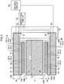
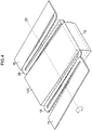
- Dispositif d'entraînement de miroir (10, 110, 210) comprenant :une unité de miroir (12) configurée pour présenter une surface de réflexion pour réfléchir de la lumière ;une paire d'unités d'actionneur piézoélectrique (14, 16) configurées pour être disposées des deux côtés de l'unité de miroir (12) de manière à enserrer l'unité de miroir (12) ;des unités de liaison (18, 20), dont chacune est configurée pour connecter une première extrémité de l'unité d'actionneur piézoélectrique (14, 16) avec une partie d'extrémité de l'unité de miroir (12), la partie d'extrémité de l'unité de miroir (12) étant à l'écart d'un axe de rotation (22) de l'unité de miroir (12) dans une direction qui est le long de la surface de réflexion et est perpendiculaire à l'axe de rotation (22) ; etune unité de fixation (30) configurée pour supporter l'autre extrémité de l'unité d'actionneur piézoélectrique (14, 16),dans lequel chacune des unités de liaison (18, 20) est une unité de charnière en forme de plaque qui présente une structure incluant deux éléments en forme de plaque (19) ou plus dont une direction longitudinale est une direction qui est le long de la surface de réflexion et qui est perpendiculaire à l'axe de rotation (22), et dans les unités de liaison (18, 20), les éléments en forme de plaque (19) sont déformés de manière à être déviés dans une direction d'épaisseur par un entraînement de l'unité d'actionneur piézoélectrique (14, 16), et chacune des unités de liaison (18, 20) est pourvue d'une unité de détection de contrainte (24-i, 125-i, 225-i) qui détecte une contrainte devant être générée dans l'unité de liaison (18, 20) pendant un entraînement en rotation de l'unité de miroir (12) par une vibration résonante, la vibration résonante étant induite par l'entraînement des unités d'actionneur piézoélectrique (14, 16) et impliquant un mouvement en rotation de l'unité de miroir (12) ;dans lequel chacune des unités de liaison (18, 20) présente une structure dans laquelle deux ou plus des éléments en forme de plaque (19) sont disposés en réseau de manière à être repliés en une forme sinueuse, et au moment de la vibration résonante, des éléments en forme de plaque (19) disposés en réseau de manière adjacente sont déformés de manière à être déviés dans des directions opposées l'une à l'autre ;caractérisé en ce que, lorsque des numéros consécutifs indiquant un ordre de réseau sont donnés aux deux ou plus des éléments en forme de plaque (19) disposés en réseau de manière à être repliés en la forme sinueuse, à partir d'un côté proche de l'unité de miroir (12) vers une direction de l'unité d'actionneur piézoélectrique (14, 16) et ainsi, chacun des éléments en forme de plaque (19) est identifié,le dispositif (10, 110, 210) comprend, en tant qu'unité de détection de contrainte (24-i),une première unité de détection de contrainte (24-2, 24-3, 125-2, 125-3, 225-2, 225-3) configurée pour détecter une contrainte devant être générée dans un élément en forme de plaque de numéro impair (19- 2, 19-3, 219-2, 219-3), etune seconde unité de détection de contrainte (24-1, 24-4, 125-1, 125-4, 225-1, 225-4) configurée pour détecter un contrainte devant être générée dans un élément en forme de plaque de numéro pair (19-1, 19-4, 219-1, 219-4).
- Dispositif d'entraînement de miroir (10, 110, 210) selon la revendication 1,
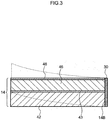
dans lequel l'unité de détection de contrainte (24-i, 125-i, 225-i) présente une structure stratifiée dans laquelle une électrode inférieure (43), une substance piézoélectrique (46) et une électrode supérieure (48) sont stratifiées sur l'élément en forme de plaque (19) dans l'ordre, et présente une structure dans laquelle la contrainte est convertie en un signal électrique par un effet piézoélectrique de la substance piézoélectrique (46). - Dispositif d'entraînement de miroir (10, 110, 210) selon la revendication 2,dans lequel des signaux de tension sont acquis à partir à la fois de la première unité de détection de contrainte (24-2, 24-3, 125-2, 125-3, 225-2, 225-3) et de la seconde unité de détection de contrainte (24-1, 24- 4, 125-1, 125-4, 225-1, 225-4), respectivement, etle dispositif d'entraînement de miroir (10, 110, 210) comprend un circuit de détection (64) configuré pour détecter un différentiel entre un premier signal de détection acquis à partir de la première unité de détection de contrainte (24-2, 24-3, 125-2, 125-3, 225-2, 225-3) et un second signal de détection acquis à partir de la seconde unité de détection de contrainte (24-1, 24 -4, 125-1, 125-4, 225-1, 225-4).
- Dispositif d'entraînement de miroir (10, 110, 210) selon la revendication 1,dans lequel une partie de surface de l'élément en forme de plaque (19) est composée d'un matériau exhibant un effet de piézo-résistance, etl'unité de détection de contrainte (24-i, 125-i, 225-i) convertit la contrainte en un changement de valeur de résistance par l'effet de piézo-résistance du matériau exhibant l'effet de piézo-résistance.
- Dispositif d'entraînement de miroir (10, 110, 210) selon la revendication 4, comprenant un circuit de détection (64) configuré pour convertir le changement de valeur de résistance en un signal de tension.
- Dispositif d'entraînement de miroir (10, 110, 210) selon la revendication 5, pour autant qu'elle se rapporte à la revendication 3,
dans lequel le circuit de détection (64) acquiert un signal de tension avec un circuit diviseur de tension configuré pour connecter une première résistance configurée par la première unité de détection de contrainte (24-2, 24-3, 125-2, 125-3, 225-2, 225-3) et une seconde résistance configurée par la seconde unité de détection de contrainte (24-1, 24-4, 125-1, 125-4, 225-1, 225-4). - Dispositif d'entraînement de miroir (10, 110, 210) selon l'une quelconque des revendications 1 à 6,
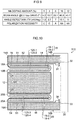
dans lequel l'unité d'actionneur piézoélectrique (14, 16) est configurée par un porte-à-faux unimorphe piézoélectrique dans lequel une plaque de vibration (42), une électrode inférieure (43), une substance piézoélectrique (46) et une électrode supérieure (48) sont stratifiées dans l'ordre. - Dispositif d'entraînement de miroir (10, 110, 210) selon la revendication 7, pour autant qu'elle se rapporte à la revendication 4,
dans lequel la substance piézoélectrique (46) à utiliser dans l'unité d'actionneur piézoélectrique (14, 16) et l'unité de détection de contrainte (24-i, 125-i, 225-i) est un film mince qui présente une épaisseur de 1 à 10 µm et qui est formé directement sur un substrat qui est la plaque de vibration (42). - Dispositif d'entraînement de miroir (10, 110, 210) selon l'une quelconque des revendications 1 à 8,dans lequel la substance piézoélectrique (46) à utiliser dans l'unité d'actionneur piézoélectrique (14, 16) est un type, ou deux types ou plus d'oxydes de type pérovskite qui sont représentés par la formule (P) suivante :
Formule Générale
ABO3... (P)
où dans la formule (P), A est un élément chimique aux sites A, et est au moins un type d'élément chimique incluant Pb,B est un élément chimique aux sites B, et est au moins un type d'élément chimique choisi dans le groupe consistant en Ti, Zr, V, Nb, Ta, Sb, Cr, Mo, W, Mn, Sc, Co, Cu, In, Sn, Ga, Zn, Cd, Fe et Ni,O est un élément oxygène, etun rapport molaire de l'élément chimique de site A, de l'élément chimique de site B et de l'élément oxygène est de 1:1:3 en tant que standard, mais le rapport molaire peut s'écarter du rapport molaire standard dans une plage permettant un structure pérovskite. - Dispositif d'entraînement de miroir (10, 110, 210) selon l'une quelconque des revendications 1 à 8,dans lequel la substance piézoélectrique (46) à utiliser dans l'unité d'actionneur piézoélectrique (14, 16) est un type de, ou deux ou plus types d'oxydes de type pérovskite qui sont représentés par la formule (PX) suivante :
Aa(Zrx, Tiy, Mb-x-y)bOc... (PX)
où dans la formule (PX), A est un élément chimique aux sites A, et est au moins un type d'élément chimique incluant Pb,M est au moins un type d'élément chimique choisi dans le groupe constitué de V, Nb, Ta et Sb,0<x<b, 0<y<b et 0 ≤ b - x - y sont maintenus, eta:b:c=1:1:3 est standard, mais le rapport molaire peut s'écarter du rapport molaire standard dans une plage permettant une structure pérovskite. - Dispositif d'entraînement de miroir (10, 110, 210) selon la revendication 10,
dans lequel l'oxyde de type pérovskite (PX) inclut du Nb, et un rapport molaire de Nb/(Zr + Ti + Nb) est de 0,06 ou plus et de 0,20 ou moins. - Dispositif d'entraînement de miroir (10, 110, 210) selon l'une quelconque des revendications 1 à 11,
dans lequel la substance piézoélectrique (46) à utiliser dans l'unité d'actionneur piézoélectrique (14, 16) est un film mince qui est formé par une procédé de pulvérisation cathodique. - Dispositif d'entraînement de miroir (10, 110, 210) selon l'une quelconque des revendications 1 à 12, comprenant
un circuit d'entraînement (62) configuré pour fournir une tension d'entraînement à la paire d'unités d'actionneur piézoélectrique (14, 16), le circuit d'entraînement (62) fournissant la tension d'entraînement qui entraîne par résonance l'unité de miroir (12) autour d'une fréquence de résonance fx dans un mode de résonance dans lequel l'unité de miroir (12) effectue un mouvement de rotation autour de l'axe de rotation (22).
Applications Claiming Priority (2)
| Application Number | Priority Date | Filing Date | Title |
|---|---|---|---|
| JP2012212238A JP5916577B2 (ja) | 2012-09-26 | 2012-09-26 | ミラー駆動装置及びその駆動方法 |
| PCT/JP2013/074648 WO2014050586A1 (fr) | 2012-09-26 | 2013-09-12 | Dispositif d'entraînement de miroir et son procédé d'entraînement |
Publications (3)
| Publication Number | Publication Date |
|---|---|
| EP2902836A1 EP2902836A1 (fr) | 2015-08-05 |
| EP2902836A4 EP2902836A4 (fr) | 2016-05-04 |
| EP2902836B1 true EP2902836B1 (fr) | 2021-10-27 |
Family
ID=50387993
Family Applications (1)
| Application Number | Title | Priority Date | Filing Date |
|---|---|---|---|
| EP13841383.6A Active EP2902836B1 (fr) | 2012-09-26 | 2013-09-12 | Dispositif d'entraînement de miroir et son procédé d'entraînement |
Country Status (4)
| Country | Link |
|---|---|
| US (1) | US10048489B2 (fr) |
| EP (1) | EP2902836B1 (fr) |
| JP (1) | JP5916577B2 (fr) |
| WO (1) | WO2014050586A1 (fr) |
Families Citing this family (22)
| Publication number | Priority date | Publication date | Assignee | Title |
|---|---|---|---|---|
| US10739460B2 (en) | 2010-08-11 | 2020-08-11 | Apple Inc. | Time-of-flight detector with single-axis scan |
| JP5654158B1 (ja) * | 2014-05-07 | 2015-01-14 | 株式会社トライフォース・マネジメント | 可動反射素子および二次元走査装置 |
| US9624100B2 (en) | 2014-06-12 | 2017-04-18 | Apple Inc. | Micro pick up array pivot mount with integrated strain sensing elements |
| DE102014217799B4 (de) * | 2014-09-05 | 2019-11-21 | Fraunhofer-Gesellschaft zur Förderung der angewandten Forschung e.V. | Piezoelektrischer Positionssensor für piezoelektrisch angetriebene resonante Mikrospiegel |
| US9705432B2 (en) * | 2014-09-30 | 2017-07-11 | Apple Inc. | Micro pick up array pivot mount design for strain amplification |
| JP6606865B2 (ja) * | 2015-05-29 | 2019-11-20 | ミツミ電機株式会社 | 光走査装置及びその製造方法、光走査制御装置 |
| JP6498047B2 (ja) | 2015-06-09 | 2019-04-10 | 株式会社トライフォース・マネジメント | 可動反射装置およびこれを利用した反射面駆動システム |
| CN104977104B (zh) * | 2015-07-13 | 2017-04-12 | 大连理工大学 | 一种压电式小量程大量程比的测力装置 |
| US10298913B2 (en) * | 2016-08-18 | 2019-05-21 | Apple Inc. | Standalone depth camera |
| IT201600132144A1 (it) * | 2016-12-29 | 2018-06-29 | St Microelectronics Srl | Dispositivo attuatore micro-elettro-meccanico con comando piezoelettrico, mobile nel piano |
| JP6354892B2 (ja) * | 2017-05-18 | 2018-07-11 | 株式会社リコー | 位置検出装置と映像機器 |
| EP3460981B1 (fr) * | 2017-07-26 | 2022-03-30 | Tri-Force Management Corporation | Élément de production d'électricité |
| DE102017220813A1 (de) | 2017-11-22 | 2019-05-23 | Robert Bosch Gmbh | Laserprojektionsvorrichtung |
| JP6985602B2 (ja) * | 2018-01-29 | 2021-12-22 | ミツミ電機株式会社 | 光走査装置及び光走査装置の製造方法 |
| IT201800002364A1 (it) | 2018-02-02 | 2019-08-02 | St Microelectronics Srl | Dispositivo micro-manipolatore micro-elettro-meccanico con comando piezoelettrico, mobile nel piano |
| DE102018215528A1 (de) * | 2018-09-12 | 2020-03-12 | Robert Bosch Gmbh | Mikromechanisches Bauteil und Herstellungsverfahren für ein mikromechanisches Bauteil |
| US11221478B2 (en) * | 2019-04-15 | 2022-01-11 | Microsoft Technology Licensing, Llc | MEMS scanner |
| US11175492B2 (en) | 2019-08-12 | 2021-11-16 | Microsoft Technology Licensing, Llc | Substrate for scanning mirror system |
| US11750779B2 (en) | 2019-08-20 | 2023-09-05 | Ricoh Company, Ltd. | Light deflector, optical scanning system, image projection device, image forming apparatus, and lidar device |
| CN112752209B (zh) * | 2019-10-31 | 2022-03-25 | 华为技术有限公司 | 一种压电式mems传感器以及相关设备 |
| CN111289155B (zh) * | 2020-02-26 | 2021-07-13 | 西安交通大学 | 基于电磁激励压阻检测的面内振动硅微谐振式压力传感器 |
| US20220026537A1 (en) * | 2020-07-22 | 2022-01-27 | Beijing Voyager Technology Co., Ltd. | Systems and methods for sensing rotation angles of a micro mirror in an optical sensing system |
Family Cites Families (10)
| Publication number | Priority date | Publication date | Assignee | Title |
|---|---|---|---|---|
| JP2008039810A (ja) * | 2006-08-01 | 2008-02-21 | Matsushita Electric Ind Co Ltd | 光学反射素子 |
| JP4926596B2 (ja) | 2006-08-08 | 2012-05-09 | スタンレー電気株式会社 | 光偏向器及びその製造方法 |
| DE102007058239B4 (de) * | 2007-12-04 | 2021-04-29 | Robert Bosch Gmbh | Mikrospiegelvorrichtung |
| JP2009258210A (ja) * | 2008-04-14 | 2009-11-05 | Panasonic Corp | 光学反射素子 |
| US8043313B2 (en) * | 2008-07-03 | 2011-10-25 | Hotspur Technologies, Inc | Apparatus and methods for treating obstructions within body lumens |
| US8477398B2 (en) * | 2009-05-11 | 2013-07-02 | Panasonic Corporation | Optical reflection element |
| JP2011095523A (ja) * | 2009-10-30 | 2011-05-12 | Panasonic Corp | 光学反射素子 |
| JP5400636B2 (ja) | 2010-01-20 | 2014-01-29 | スタンレー電気株式会社 | 光偏向器及びこれを用いた光学装置 |
| JP5293668B2 (ja) * | 2010-03-30 | 2013-09-18 | パナソニック株式会社 | 光学反射素子 |
| JP5592192B2 (ja) * | 2010-08-11 | 2014-09-17 | 富士フイルム株式会社 | 圧電体膜とその製造方法、圧電素子および液体吐出装置 |
-
2012
- 2012-09-26 JP JP2012212238A patent/JP5916577B2/ja active Active
-
2013
- 2013-09-12 WO PCT/JP2013/074648 patent/WO2014050586A1/fr active Application Filing
- 2013-09-12 EP EP13841383.6A patent/EP2902836B1/fr active Active
-
2015
- 2015-03-25 US US14/668,429 patent/US10048489B2/en active Active
Non-Patent Citations (1)
| Title |
|---|
| None * |
Also Published As
| Publication number | Publication date |
|---|---|
| EP2902836A1 (fr) | 2015-08-05 |
| US20150198801A1 (en) | 2015-07-16 |
| EP2902836A4 (fr) | 2016-05-04 |
| WO2014050586A1 (fr) | 2014-04-03 |
| US10048489B2 (en) | 2018-08-14 |
| JP5916577B2 (ja) | 2016-05-11 |
| JP2014066876A (ja) | 2014-04-17 |
Similar Documents
| Publication | Publication Date | Title |
|---|---|---|
| EP2902836B1 (fr) | Dispositif d'entraînement de miroir et son procédé d'entraînement | |
| US9864189B2 (en) | Mirror drive device and driving method thereof | |
| EP2827183B1 (fr) | Dispositif d'entraînement de miroir et son procédé de commande | |
| US8879132B2 (en) | Mirror driving apparatus, method of driving same and method of manufacturing same | |
| US9030721B2 (en) | Mirror driving device and method of controlling the device | |
| EP3203297B1 (fr) | Dispositif d'entraînement de miroir et procédé d'entraînement pour celui-ci | |
| JP5264954B2 (ja) | ミラー駆動装置及び方法 | |
| EP3203298B1 (fr) | Dispositif d'entraînement de miroir et son procédé d'entraînement | |
| US20210223539A1 (en) | Micromirror device and method of driving micromirror device | |
| JP5344110B1 (ja) | 圧電体膜、インクジェットヘッド、インクジェットヘッドを用いて画像を形成する方法、角速度センサ、角速度センサを用いて角速度を測定する方法、圧電発電素子ならびに圧電発電素子を用いた発電方法 |
Legal Events
| Date | Code | Title | Description |
|---|---|---|---|
| PUAI | Public reference made under article 153(3) epc to a published international application that has entered the european phase |
Free format text: ORIGINAL CODE: 0009012 |
|
| 17P | Request for examination filed |
Effective date: 20150325 |
|
| AK | Designated contracting states |
Kind code of ref document: A1 Designated state(s): AL AT BE BG CH CY CZ DE DK EE ES FI FR GB GR HR HU IE IS IT LI LT LU LV MC MK MT NL NO PL PT RO RS SE SI SK SM TR |
|
| AX | Request for extension of the european patent |
Extension state: BA ME |
|
| DAX | Request for extension of the european patent (deleted) | ||
| RA4 | Supplementary search report drawn up and despatched (corrected) |
Effective date: 20160406 |
|
| RIC1 | Information provided on ipc code assigned before grant |
Ipc: H01L 41/09 20060101ALI20160331BHEP Ipc: G02B 26/08 20060101ALI20160331BHEP Ipc: G02B 26/10 20060101AFI20160331BHEP Ipc: B81B 3/00 20060101ALI20160331BHEP Ipc: H01L 41/187 20060101ALI20160331BHEP |
|
| STAA | Information on the status of an ep patent application or granted ep patent |
Free format text: STATUS: EXAMINATION IS IN PROGRESS |
|
| 17Q | First examination report despatched |
Effective date: 20190219 |
|
| STAA | Information on the status of an ep patent application or granted ep patent |
Free format text: STATUS: EXAMINATION IS IN PROGRESS |
|
| RAP3 | Party data changed (applicant data changed or rights of an application transferred) |
Owner name: FUJIFILM CORPORATION |
|
| GRAP | Despatch of communication of intention to grant a patent |
Free format text: ORIGINAL CODE: EPIDOSNIGR1 |
|
| STAA | Information on the status of an ep patent application or granted ep patent |
Free format text: STATUS: GRANT OF PATENT IS INTENDED |
|
| INTG | Intention to grant announced |
Effective date: 20210629 |
|
| GRAS | Grant fee paid |
Free format text: ORIGINAL CODE: EPIDOSNIGR3 |
|
| GRAA | (expected) grant |
Free format text: ORIGINAL CODE: 0009210 |
|
| STAA | Information on the status of an ep patent application or granted ep patent |
Free format text: STATUS: THE PATENT HAS BEEN GRANTED |
|
| AK | Designated contracting states |
Kind code of ref document: B1 Designated state(s): AL AT BE BG CH CY CZ DE DK EE ES FI FR GB GR HR HU IE IS IT LI LT LU LV MC MK MT NL NO PL PT RO RS SE SI SK SM TR |
|
| REG | Reference to a national code |
Ref country code: GB Ref legal event code: FG4D |
|
| REG | Reference to a national code |
Ref country code: CH Ref legal event code: EP |
|
| REG | Reference to a national code |
Ref country code: AT Ref legal event code: REF Ref document number: 1442297 Country of ref document: AT Kind code of ref document: T Effective date: 20211115 |
|
| REG | Reference to a national code |
Ref country code: DE Ref legal event code: R096 Ref document number: 602013079830 Country of ref document: DE |
|
| REG | Reference to a national code |
Ref country code: IE Ref legal event code: FG4D |
|
| REG | Reference to a national code |
Ref country code: LT Ref legal event code: MG9D |
|
| REG | Reference to a national code |
Ref country code: NL Ref legal event code: MP Effective date: 20211027 |
|
| REG | Reference to a national code |
Ref country code: AT Ref legal event code: MK05 Ref document number: 1442297 Country of ref document: AT Kind code of ref document: T Effective date: 20211027 |
|
| PG25 | Lapsed in a contracting state [announced via postgrant information from national office to epo] |
Ref country code: RS Free format text: LAPSE BECAUSE OF FAILURE TO SUBMIT A TRANSLATION OF THE DESCRIPTION OR TO PAY THE FEE WITHIN THE PRESCRIBED TIME-LIMIT Effective date: 20211027 Ref country code: LT Free format text: LAPSE BECAUSE OF FAILURE TO SUBMIT A TRANSLATION OF THE DESCRIPTION OR TO PAY THE FEE WITHIN THE PRESCRIBED TIME-LIMIT Effective date: 20211027 Ref country code: FI Free format text: LAPSE BECAUSE OF FAILURE TO SUBMIT A TRANSLATION OF THE DESCRIPTION OR TO PAY THE FEE WITHIN THE PRESCRIBED TIME-LIMIT Effective date: 20211027 Ref country code: BG Free format text: LAPSE BECAUSE OF FAILURE TO SUBMIT A TRANSLATION OF THE DESCRIPTION OR TO PAY THE FEE WITHIN THE PRESCRIBED TIME-LIMIT Effective date: 20220127 Ref country code: AT Free format text: LAPSE BECAUSE OF FAILURE TO SUBMIT A TRANSLATION OF THE DESCRIPTION OR TO PAY THE FEE WITHIN THE PRESCRIBED TIME-LIMIT Effective date: 20211027 |
|
| PG25 | Lapsed in a contracting state [announced via postgrant information from national office to epo] |
Ref country code: IS Free format text: LAPSE BECAUSE OF FAILURE TO SUBMIT A TRANSLATION OF THE DESCRIPTION OR TO PAY THE FEE WITHIN THE PRESCRIBED TIME-LIMIT Effective date: 20220227 Ref country code: SE Free format text: LAPSE BECAUSE OF FAILURE TO SUBMIT A TRANSLATION OF THE DESCRIPTION OR TO PAY THE FEE WITHIN THE PRESCRIBED TIME-LIMIT Effective date: 20211027 Ref country code: PT Free format text: LAPSE BECAUSE OF FAILURE TO SUBMIT A TRANSLATION OF THE DESCRIPTION OR TO PAY THE FEE WITHIN THE PRESCRIBED TIME-LIMIT Effective date: 20220228 Ref country code: PL Free format text: LAPSE BECAUSE OF FAILURE TO SUBMIT A TRANSLATION OF THE DESCRIPTION OR TO PAY THE FEE WITHIN THE PRESCRIBED TIME-LIMIT Effective date: 20211027 Ref country code: NO Free format text: LAPSE BECAUSE OF FAILURE TO SUBMIT A TRANSLATION OF THE DESCRIPTION OR TO PAY THE FEE WITHIN THE PRESCRIBED TIME-LIMIT Effective date: 20220127 Ref country code: NL Free format text: LAPSE BECAUSE OF FAILURE TO SUBMIT A TRANSLATION OF THE DESCRIPTION OR TO PAY THE FEE WITHIN THE PRESCRIBED TIME-LIMIT Effective date: 20211027 Ref country code: LV Free format text: LAPSE BECAUSE OF FAILURE TO SUBMIT A TRANSLATION OF THE DESCRIPTION OR TO PAY THE FEE WITHIN THE PRESCRIBED TIME-LIMIT Effective date: 20211027 Ref country code: HR Free format text: LAPSE BECAUSE OF FAILURE TO SUBMIT A TRANSLATION OF THE DESCRIPTION OR TO PAY THE FEE WITHIN THE PRESCRIBED TIME-LIMIT Effective date: 20211027 Ref country code: GR Free format text: LAPSE BECAUSE OF FAILURE TO SUBMIT A TRANSLATION OF THE DESCRIPTION OR TO PAY THE FEE WITHIN THE PRESCRIBED TIME-LIMIT Effective date: 20220128 Ref country code: ES Free format text: LAPSE BECAUSE OF FAILURE TO SUBMIT A TRANSLATION OF THE DESCRIPTION OR TO PAY THE FEE WITHIN THE PRESCRIBED TIME-LIMIT Effective date: 20211027 |
|
| REG | Reference to a national code |
Ref country code: DE Ref legal event code: R097 Ref document number: 602013079830 Country of ref document: DE |
|
| PG25 | Lapsed in a contracting state [announced via postgrant information from national office to epo] |
Ref country code: SM Free format text: LAPSE BECAUSE OF FAILURE TO SUBMIT A TRANSLATION OF THE DESCRIPTION OR TO PAY THE FEE WITHIN THE PRESCRIBED TIME-LIMIT Effective date: 20211027 Ref country code: SK Free format text: LAPSE BECAUSE OF FAILURE TO SUBMIT A TRANSLATION OF THE DESCRIPTION OR TO PAY THE FEE WITHIN THE PRESCRIBED TIME-LIMIT Effective date: 20211027 Ref country code: RO Free format text: LAPSE BECAUSE OF FAILURE TO SUBMIT A TRANSLATION OF THE DESCRIPTION OR TO PAY THE FEE WITHIN THE PRESCRIBED TIME-LIMIT Effective date: 20211027 Ref country code: EE Free format text: LAPSE BECAUSE OF FAILURE TO SUBMIT A TRANSLATION OF THE DESCRIPTION OR TO PAY THE FEE WITHIN THE PRESCRIBED TIME-LIMIT Effective date: 20211027 Ref country code: DK Free format text: LAPSE BECAUSE OF FAILURE TO SUBMIT A TRANSLATION OF THE DESCRIPTION OR TO PAY THE FEE WITHIN THE PRESCRIBED TIME-LIMIT Effective date: 20211027 Ref country code: CZ Free format text: LAPSE BECAUSE OF FAILURE TO SUBMIT A TRANSLATION OF THE DESCRIPTION OR TO PAY THE FEE WITHIN THE PRESCRIBED TIME-LIMIT Effective date: 20211027 |
|
| PLBE | No opposition filed within time limit |
Free format text: ORIGINAL CODE: 0009261 |
|
| STAA | Information on the status of an ep patent application or granted ep patent |
Free format text: STATUS: NO OPPOSITION FILED WITHIN TIME LIMIT |
|
| 26N | No opposition filed |
Effective date: 20220728 |
|
| PG25 | Lapsed in a contracting state [announced via postgrant information from national office to epo] |
Ref country code: AL Free format text: LAPSE BECAUSE OF FAILURE TO SUBMIT A TRANSLATION OF THE DESCRIPTION OR TO PAY THE FEE WITHIN THE PRESCRIBED TIME-LIMIT Effective date: 20211027 |
|
| PG25 | Lapsed in a contracting state [announced via postgrant information from national office to epo] |
Ref country code: SI Free format text: LAPSE BECAUSE OF FAILURE TO SUBMIT A TRANSLATION OF THE DESCRIPTION OR TO PAY THE FEE WITHIN THE PRESCRIBED TIME-LIMIT Effective date: 20211027 |
|
| PG25 | Lapsed in a contracting state [announced via postgrant information from national office to epo] |
Ref country code: MC Free format text: LAPSE BECAUSE OF FAILURE TO SUBMIT A TRANSLATION OF THE DESCRIPTION OR TO PAY THE FEE WITHIN THE PRESCRIBED TIME-LIMIT Effective date: 20211027 |
|
| REG | Reference to a national code |
Ref country code: CH Ref legal event code: PL |
|
| REG | Reference to a national code |
Ref country code: BE Ref legal event code: MM Effective date: 20220930 |
|
| PG25 | Lapsed in a contracting state [announced via postgrant information from national office to epo] |
Ref country code: IT Free format text: LAPSE BECAUSE OF FAILURE TO SUBMIT A TRANSLATION OF THE DESCRIPTION OR TO PAY THE FEE WITHIN THE PRESCRIBED TIME-LIMIT Effective date: 20211027 |
|
| P01 | Opt-out of the competence of the unified patent court (upc) registered |
Effective date: 20230515 |
|
| PG25 | Lapsed in a contracting state [announced via postgrant information from national office to epo] |
Ref country code: LU Free format text: LAPSE BECAUSE OF NON-PAYMENT OF DUE FEES Effective date: 20220912 |
|
| PG25 | Lapsed in a contracting state [announced via postgrant information from national office to epo] |
Ref country code: LI Free format text: LAPSE BECAUSE OF NON-PAYMENT OF DUE FEES Effective date: 20220930 Ref country code: IE Free format text: LAPSE BECAUSE OF NON-PAYMENT OF DUE FEES Effective date: 20220912 Ref country code: CH Free format text: LAPSE BECAUSE OF NON-PAYMENT OF DUE FEES Effective date: 20220930 |
|
| PG25 | Lapsed in a contracting state [announced via postgrant information from national office to epo] |
Ref country code: BE Free format text: LAPSE BECAUSE OF NON-PAYMENT OF DUE FEES Effective date: 20220930 |
|
| PGFP | Annual fee paid to national office [announced via postgrant information from national office to epo] |
Ref country code: GB Payment date: 20230727 Year of fee payment: 11 |
|
| PGFP | Annual fee paid to national office [announced via postgrant information from national office to epo] |
Ref country code: FR Payment date: 20230808 Year of fee payment: 11 Ref country code: DE Payment date: 20230802 Year of fee payment: 11 |
|
| PG25 | Lapsed in a contracting state [announced via postgrant information from national office to epo] |
Ref country code: HU Free format text: LAPSE BECAUSE OF FAILURE TO SUBMIT A TRANSLATION OF THE DESCRIPTION OR TO PAY THE FEE WITHIN THE PRESCRIBED TIME-LIMIT; INVALID AB INITIO Effective date: 20130912 |