EP2827183B1 - Dispositif d'entraînement de miroir et son procédé de commande - Google Patents
Dispositif d'entraînement de miroir et son procédé de commande Download PDFInfo
- Publication number
- EP2827183B1 EP2827183B1 EP14177045.3A EP14177045A EP2827183B1 EP 2827183 B1 EP2827183 B1 EP 2827183B1 EP 14177045 A EP14177045 A EP 14177045A EP 2827183 B1 EP2827183 B1 EP 2827183B1
- Authority
- EP
- European Patent Office
- Prior art keywords
- section
- electrode
- actuator
- mirror
- piezoelectric
- Prior art date
- Legal status (The legal status is an assumption and is not a legal conclusion. Google has not performed a legal analysis and makes no representation as to the accuracy of the status listed.)
- Active
Links
- 238000000034 method Methods 0.000 title claims description 36
- 238000001514 detection method Methods 0.000 claims description 50
- 238000006073 displacement reaction Methods 0.000 claims description 39
- 230000008878 coupling Effects 0.000 claims description 37
- 238000010168 coupling process Methods 0.000 claims description 37
- 238000005859 coupling reaction Methods 0.000 claims description 37
- 239000010409 thin film Substances 0.000 claims description 18
- 239000000758 substrate Substances 0.000 claims description 17
- 238000009826 distribution Methods 0.000 claims description 13
- 230000000694 effects Effects 0.000 claims description 12
- 238000003475 lamination Methods 0.000 claims description 11
- 238000007667 floating Methods 0.000 claims description 10
- 229910052787 antimony Inorganic materials 0.000 claims description 4
- QVGXLLKOCUKJST-UHFFFAOYSA-N atomic oxygen Chemical compound [O] QVGXLLKOCUKJST-UHFFFAOYSA-N 0.000 claims description 4
- 229910052758 niobium Inorganic materials 0.000 claims description 4
- 239000001301 oxygen Substances 0.000 claims description 4
- 229910052760 oxygen Inorganic materials 0.000 claims description 4
- 229910052715 tantalum Inorganic materials 0.000 claims description 4
- 229910052720 vanadium Inorganic materials 0.000 claims description 4
- 238000005452 bending Methods 0.000 claims description 3
- 229910052759 nickel Inorganic materials 0.000 claims description 3
- 229910052719 titanium Inorganic materials 0.000 claims description 3
- 229910052726 zirconium Inorganic materials 0.000 claims description 3
- 229910052793 cadmium Inorganic materials 0.000 claims description 2
- 229910052804 chromium Inorganic materials 0.000 claims description 2
- 229910052802 copper Inorganic materials 0.000 claims description 2
- 229910052733 gallium Inorganic materials 0.000 claims description 2
- 229910052738 indium Inorganic materials 0.000 claims description 2
- 229910052742 iron Inorganic materials 0.000 claims description 2
- 229910052748 manganese Inorganic materials 0.000 claims description 2
- 229910052750 molybdenum Inorganic materials 0.000 claims description 2
- 229910052706 scandium Inorganic materials 0.000 claims description 2
- 229910052718 tin Inorganic materials 0.000 claims description 2
- 229910052721 tungsten Inorganic materials 0.000 claims description 2
- 229910052725 zinc Inorganic materials 0.000 claims description 2
- 239000012071 phase Substances 0.000 description 45
- 230000000052 comparative effect Effects 0.000 description 35
- 238000010586 diagram Methods 0.000 description 29
- 230000003287 optical effect Effects 0.000 description 16
- 239000010408 film Substances 0.000 description 14
- 238000002474 experimental method Methods 0.000 description 13
- 230000006835 compression Effects 0.000 description 12
- 238000007906 compression Methods 0.000 description 12
- 238000012986 modification Methods 0.000 description 9
- 230000004048 modification Effects 0.000 description 9
- 239000000463 material Substances 0.000 description 8
- 238000009413 insulation Methods 0.000 description 7
- 238000004458 analytical method Methods 0.000 description 5
- 238000004519 manufacturing process Methods 0.000 description 5
- 239000000203 mixture Substances 0.000 description 5
- 238000004544 sputter deposition Methods 0.000 description 5
- XUIMIQQOPSSXEZ-UHFFFAOYSA-N Silicon Chemical compound [Si] XUIMIQQOPSSXEZ-UHFFFAOYSA-N 0.000 description 4
- 150000001875 compounds Chemical class 0.000 description 4
- 150000002500 ions Chemical class 0.000 description 4
- 230000008569 process Effects 0.000 description 4
- 229910052710 silicon Inorganic materials 0.000 description 4
- 239000010703 silicon Substances 0.000 description 4
- 239000013598 vector Substances 0.000 description 4
- 229910002113 barium titanate Inorganic materials 0.000 description 3
- 238000006243 chemical reaction Methods 0.000 description 3
- 238000013461 design Methods 0.000 description 3
- 238000001312 dry etching Methods 0.000 description 3
- 238000005530 etching Methods 0.000 description 3
- 238000011156 evaluation Methods 0.000 description 3
- HFGPZNIAWCZYJU-UHFFFAOYSA-N lead zirconate titanate Chemical compound [O-2].[O-2].[O-2].[O-2].[O-2].[Ti+4].[Zr+4].[Pb+2] HFGPZNIAWCZYJU-UHFFFAOYSA-N 0.000 description 3
- PXHVJJICTQNCMI-UHFFFAOYSA-N nickel Substances [Ni] PXHVJJICTQNCMI-UHFFFAOYSA-N 0.000 description 3
- 238000001947 vapour-phase growth Methods 0.000 description 3
- RTAQQCXQSZGOHL-UHFFFAOYSA-N Titanium Chemical compound [Ti] RTAQQCXQSZGOHL-UHFFFAOYSA-N 0.000 description 2
- 125000004429 atom Chemical group 0.000 description 2
- 239000013078 crystal Substances 0.000 description 2
- 230000007547 defect Effects 0.000 description 2
- 239000007789 gas Substances 0.000 description 2
- 239000010931 gold Substances 0.000 description 2
- 230000005484 gravity Effects 0.000 description 2
- 229910052746 lanthanum Inorganic materials 0.000 description 2
- FZLIPJUXYLNCLC-UHFFFAOYSA-N lanthanum atom Chemical compound [La] FZLIPJUXYLNCLC-UHFFFAOYSA-N 0.000 description 2
- 229910052451 lead zirconate titanate Inorganic materials 0.000 description 2
- QNZFKUWECYSYPS-UHFFFAOYSA-N lead zirconium Chemical compound [Zr].[Pb] QNZFKUWECYSYPS-UHFFFAOYSA-N 0.000 description 2
- 238000005259 measurement Methods 0.000 description 2
- 229910052751 metal Inorganic materials 0.000 description 2
- 239000002184 metal Substances 0.000 description 2
- 230000011218 segmentation Effects 0.000 description 2
- 238000003980 solgel method Methods 0.000 description 2
- 229910002902 BiFeO3 Inorganic materials 0.000 description 1
- -1 KNaNbO3 Inorganic materials 0.000 description 1
- FYYHWMGAXLPEAU-UHFFFAOYSA-N Magnesium Chemical compound [Mg] FYYHWMGAXLPEAU-UHFFFAOYSA-N 0.000 description 1
- YPQJHZKJHIBJAP-UHFFFAOYSA-N [K].[Bi] Chemical compound [K].[Bi] YPQJHZKJHIBJAP-UHFFFAOYSA-N 0.000 description 1
- WOIHABYNKOEWFG-UHFFFAOYSA-N [Sr].[Ba] Chemical compound [Sr].[Ba] WOIHABYNKOEWFG-UHFFFAOYSA-N 0.000 description 1
- 230000009471 action Effects 0.000 description 1
- 229910052782 aluminium Inorganic materials 0.000 description 1
- XAGFODPZIPBFFR-UHFFFAOYSA-N aluminium Chemical compound [Al] XAGFODPZIPBFFR-UHFFFAOYSA-N 0.000 description 1
- JRPBQTZRNDNNOP-UHFFFAOYSA-N barium titanate Chemical compound [Ba+2].[Ba+2].[O-][Ti]([O-])([O-])[O-] JRPBQTZRNDNNOP-UHFFFAOYSA-N 0.000 description 1
- 230000008901 benefit Effects 0.000 description 1
- 229910052797 bismuth Inorganic materials 0.000 description 1
- JCXGWMGPZLAOME-UHFFFAOYSA-N bismuth atom Chemical compound [Bi] JCXGWMGPZLAOME-UHFFFAOYSA-N 0.000 description 1
- FSAJRXGMUISOIW-UHFFFAOYSA-N bismuth sodium Chemical compound [Na].[Bi] FSAJRXGMUISOIW-UHFFFAOYSA-N 0.000 description 1
- 238000005229 chemical vapour deposition Methods 0.000 description 1
- 239000011248 coating agent Substances 0.000 description 1
- 238000000576 coating method Methods 0.000 description 1
- 238000004891 communication Methods 0.000 description 1
- 230000001419 dependent effect Effects 0.000 description 1
- 238000000151 deposition Methods 0.000 description 1
- 230000008021 deposition Effects 0.000 description 1
- NKZSPGSOXYXWQA-UHFFFAOYSA-N dioxido(oxo)titanium;lead(2+) Chemical compound [Pb+2].[O-][Ti]([O-])=O NKZSPGSOXYXWQA-UHFFFAOYSA-N 0.000 description 1
- 238000005516 engineering process Methods 0.000 description 1
- PCHJSUWPFVWCPO-UHFFFAOYSA-N gold Chemical compound [Au] PCHJSUWPFVWCPO-UHFFFAOYSA-N 0.000 description 1
- 229910052737 gold Inorganic materials 0.000 description 1
- 238000009616 inductively coupled plasma Methods 0.000 description 1
- 239000012212 insulator Substances 0.000 description 1
- 238000007733 ion plating Methods 0.000 description 1
- GQYHUHYESMUTHG-UHFFFAOYSA-N lithium niobate Chemical compound [Li+].[O-][Nb](=O)=O GQYHUHYESMUTHG-UHFFFAOYSA-N 0.000 description 1
- 229910052749 magnesium Inorganic materials 0.000 description 1
- 239000011777 magnesium Substances 0.000 description 1
- 238000012014 optical coherence tomography Methods 0.000 description 1
- 125000004430 oxygen atom Chemical group O* 0.000 description 1
- 238000000059 patterning Methods 0.000 description 1
- 230000010363 phase shift Effects 0.000 description 1
- 238000001020 plasma etching Methods 0.000 description 1
- 230000010287 polarization Effects 0.000 description 1
- UKDIAJWKFXFVFG-UHFFFAOYSA-N potassium;oxido(dioxo)niobium Chemical compound [K+].[O-][Nb](=O)=O UKDIAJWKFXFVFG-UHFFFAOYSA-N 0.000 description 1
- 238000004088 simulation Methods 0.000 description 1
- UYLYBEXRJGPQSH-UHFFFAOYSA-N sodium;oxido(dioxo)niobium Chemical compound [Na+].[O-][Nb](=O)=O UYLYBEXRJGPQSH-UHFFFAOYSA-N 0.000 description 1
- 239000000126 substance Substances 0.000 description 1
- 239000013077 target material Substances 0.000 description 1
- 238000004876 x-ray fluorescence Methods 0.000 description 1
- 239000011701 zinc Substances 0.000 description 1
- RPEUFVJJAJYJSS-UHFFFAOYSA-N zinc;oxido(dioxo)niobium Chemical compound [Zn+2].[O-][Nb](=O)=O.[O-][Nb](=O)=O RPEUFVJJAJYJSS-UHFFFAOYSA-N 0.000 description 1
- 229910000859 α-Fe Inorganic materials 0.000 description 1
Images


Classifications
-
- G—PHYSICS
- G02—OPTICS
- G02B—OPTICAL ELEMENTS, SYSTEMS OR APPARATUS
- G02B26/00—Optical devices or arrangements for the control of light using movable or deformable optical elements
- G02B26/08—Optical devices or arrangements for the control of light using movable or deformable optical elements for controlling the direction of light
- G02B26/0816—Optical devices or arrangements for the control of light using movable or deformable optical elements for controlling the direction of light by means of one or more reflecting elements
- G02B26/0833—Optical devices or arrangements for the control of light using movable or deformable optical elements for controlling the direction of light by means of one or more reflecting elements the reflecting element being a micromechanical device, e.g. a MEMS mirror, DMD
- G02B26/0858—Optical devices or arrangements for the control of light using movable or deformable optical elements for controlling the direction of light by means of one or more reflecting elements the reflecting element being a micromechanical device, e.g. a MEMS mirror, DMD the reflecting means being moved or deformed by piezoelectric means
-
- B—PERFORMING OPERATIONS; TRANSPORTING
- B81—MICROSTRUCTURAL TECHNOLOGY
- B81B—MICROSTRUCTURAL DEVICES OR SYSTEMS, e.g. MICROMECHANICAL DEVICES
- B81B3/00—Devices comprising flexible or deformable elements, e.g. comprising elastic tongues or membranes
-
- H—ELECTRICITY
- H02—GENERATION; CONVERSION OR DISTRIBUTION OF ELECTRIC POWER
- H02N—ELECTRIC MACHINES NOT OTHERWISE PROVIDED FOR
- H02N2/00—Electric machines in general using piezoelectric effect, electrostriction or magnetostriction
- H02N2/10—Electric machines in general using piezoelectric effect, electrostriction or magnetostriction producing rotary motion, e.g. rotary motors
- H02N2/103—Electric machines in general using piezoelectric effect, electrostriction or magnetostriction producing rotary motion, e.g. rotary motors by pressing one or more vibrators against the rotor
-
- H—ELECTRICITY
- H02—GENERATION; CONVERSION OR DISTRIBUTION OF ELECTRIC POWER
- H02N—ELECTRIC MACHINES NOT OTHERWISE PROVIDED FOR
- H02N2/00—Electric machines in general using piezoelectric effect, electrostriction or magnetostriction
- H02N2/10—Electric machines in general using piezoelectric effect, electrostriction or magnetostriction producing rotary motion, e.g. rotary motors
- H02N2/14—Drive circuits; Control arrangements or methods
- H02N2/145—Large signal circuits, e.g. final stages
- H02N2/147—Multi-phase circuits
-
- H—ELECTRICITY
- H10—SEMICONDUCTOR DEVICES; ELECTRIC SOLID-STATE DEVICES NOT OTHERWISE PROVIDED FOR
- H10N—ELECTRIC SOLID-STATE DEVICES NOT OTHERWISE PROVIDED FOR
- H10N30/00—Piezoelectric or electrostrictive devices
- H10N30/20—Piezoelectric or electrostrictive devices with electrical input and mechanical output, e.g. functioning as actuators or vibrators
- H10N30/204—Piezoelectric or electrostrictive devices with electrical input and mechanical output, e.g. functioning as actuators or vibrators using bending displacement, e.g. unimorph, bimorph or multimorph cantilever or membrane benders
- H10N30/2041—Beam type
Definitions
- the presently disclosed subject matter is related to a mirror drive device and a driving method of the mirror drive device, and in particular, related to a structure of a micro mirror device that is suitable for an optical deflector that is used for optical scanning, and a driving method of the micro mirror device.
- micro electro mechanical system (MEMS) scanner A micro scanner that is manufactured using a micro process technology of silicon (Si) (hereinafter referred to as “micro electro mechanical system (MEMS) scanner”) features a small size and low power consumption, and a wide range of applications from a laser projector to an optical diagnostic scanner such as for optical coherence tomography have been expected.
- Si silicon
- MEMS micro electro mechanical system
- a piezoelectric driving scheme using deformation of a piezoelectric body has a high torque density as compared with the other schemes, and obtains a high scan angle with the small size, so that the piezoelectric drive scheme is promising among the various schemes.
- resonance driving is mainly used, and the high torque of the piezoelectric driving scheme is a great advantage for the utilization.
- US 2010/0195180 A1 relates to a deflecting mirror which includes a fixed base member; a mirror having a reflection surface; a support member swingably supporting the mirror; a pair of driving beam members, each having a first end connected with the fixed base member and a second end connected with the support member to support the support member from both sides; and a piezoelectric member fixed to each driving beam member and extending from the first or second end of each driving beam member while having length not longer than about half the length of the driving beam member.
- the piezoelectric member and the driving beam members constitute piezoelectric unimorph or bimorph structure.
- JP 2010/26069 , JP 2005/128147 A , and JP 2013/112342 A are further prior art.
- the piezoelectric MEMS scanner having such a structure cannot convert the piezoelectric torque into tilting displacement effectively, and high voltage of about 40V (volts) is required in order to obtain a sufficient displacement angle.
- a sensor stress detection section
- drive displacement is required in order to keep vibration in a resonant mode, and in this case, it is necessary that one of the cantilevers in the actuator is used as a sensor, so that there is a problem that driving force is significantly reduced to about half.
- the presently disclosed subject matter is made in view of such circumstances, and an object of the presently disclosed subject matter is to provide a mirror drive device in which a displacement efficiency can be improved as compared with the conventional structure, and a displacement angle that is large enough can be obtained even when a sensor section is provided, and a driving method of the mirror drive device.
- the electrode section is arranged correspondingly to distribution of stresses that are generated in the piezoelectric body at the time of deformation of the actuator section, so that driving can be performed efficiently, and a larger mirror inclination angle can be obtained as compared with the structure in the related art.
- the displacement efficiency is improved, so that a sufficient displacement angle can be obtained even when the part of electrodes is used for the detection.
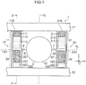
- Fig. 1 is a plan view of a structure of a micro scanner device according to a first embodiment not falling under the scope of claim 1.
- a micro scanner device 1 that corresponds to "mirror drive device” includes a mirror section 2 having a circular shape, a first torsion bar section 4 and a second torsion bar section 7 that support the mirror section 2 from both sides of the diameter direction, a first actuator section 11 and a second actuator section 22 that are connected to the first torsion bar section 4 and operate as a piezoelectric actuator section 10, a third actuator section 31 and a fourth actuator section 42 that are connected to a second torsion bar section 7 and operate as a piezoelectric actuator section 30.
- the first actuator section 11 and the second actuator section 22 are connected to each other through a coupling section 15, and the first torsion bar section 4 is connected to the coupling section 15.
- the third actuator section 31 and the fourth actuator section 42 are connected to each other through a coupling section 35, and the second torsion bar section 7 is connected to the coupling section 35.
- the micro scanner device 1 includes a first fixture member 51 to and by which a base end section 11B that is an end portion on the opposite side to the coupling section 15 of the first actuator section 11 is fixed and supported and a second fixture member 52 to and by which a base end section 22B that is an end portion on the opposite side to the coupling section 15 of the second actuator section 22 is fixed and supported.
- first fixture member 51 and the second fixture member 52 can be a part of a fixture frame member in which members are connected to each other integrally through a member element that is not illustrated.
- the first torsion bar section 4 and the second torsion bar section 7 are members that supports the mirror section 2 rotatably, and correspond "mirror supporting section", and the first torsion bar section 4 corresponds to “first mirror supporting section”, and the second torsion bar section 7 corresponds to "second mirror supporting section".
- the base end sections 11B and 31B correspond to "first base end section", the base end sections 22B and 42B correspond to "second base end section”.
- the first fixture member 51 and the second fixture member 52 correspond to "fixture section".
- x, y, and z axes that are perpendicular to each other is described in which a normal line direction of the mirror surface (reflective surface 2C) at the time of non-driving of the piezoelectric actuator sections 10 and 30 is set as a z axis direction (direction perpendicular to the plane of Fig. 1 ), and a direction that is parallel to a rotating axis (main axis) R A of the mirror section 2 by the first torsion bar section 4 and the second torsion bar section 7 (horizontal direction parallel to the plane of Fig.
- a direction that is perpendicular to both the x axis and the z axis (vertical direction parallel to the plane of Fig. 1 ) is set as a y axis direction.
- the micro scanner device 1 is parallel to the y axis and has a structure of a line symmetry (left-right symmetry) generally with respect to the center line CL that passes through the center of the mirror section 2. Due to the symmetry on such a structure, the first actuator section 11 and the third actuator section 31 have the same the structure and function, and the structures and functions of the second actuator section 22 and the fourth actuator section 42 are in common. That is, the third actuator section 31 and the fourth actuator section 42 have structures that are respectively similar to the first actuator section 11 and the second actuator section 22, and the third actuator section 31 corresponds to "first actuator section", and the fourth actuator section 42 correspond to "second actuator section".
- the upper surface of the mirror section 2 is a reflective surface 2C that reflects light.
- a metal thin film such as Au (gold) and Al (aluminum) is formed in order to improve a reflectance of incident light.
- the material and film thickness that are used for mirror coating are not limited, and various designs can be made using a known mirror material (high reflectance material).
- the planar shape of the mirror section 2 that functions as a reflection section and the shape of the reflective surface 2C may correspond to each other, or may be different from each other.
- the reflective surface 2C can be formed within an area range of the upper surface of the mirror section 2.
- the mirror section 2 having a circular shape is illustrated, but in the embodiments, the shape of the mirror section 2 is not particularly limited. Instead of the circular shape illustrated in Fig. 1 , various shapes such as oval, square, or polygon shape can be employed.
- the representation of the circular, oval, rectangle (square) shapes, etc. means that, the shape can be regarded as the basic overall shape of these configurations substantially regardless of the shape in the strict mathematical definition.
- a rectangle shape the corners of which are chamfered a rectangle shape the corners are rounded, a shape in which a part or all of lines are constituted by a curve and a polygonal line, a shape to which an additional shape is added that is required for a connection portion of the mirror section 2, and the first torsion bar section 4 and the second torsion bar section 7.
- the first actuator section 11 and the second actuator section 22 are coupled to each other in the y axis direction so that the axes of the respective longitudinal directions are matched to each other.
- the first torsion bar section 4 is connected to the coupling section 15 of the first actuator section 11 and the second actuator section 22. That is, the coupling section 15 is a connection portion between the first actuator section 11 and the second actuator section 22, and a connection portion between the first actuator section 11, the second actuator section 22, and the first torsion bar section 4.
- the first actuator section 11 and the second actuator section 22 are arranged on the both sides of the y axis direction (both upper and lower sides in Fig. 1 ) across the coupling section 15 to which the first torsion bar section 4 is connected. In Fig.
- the first actuator section 11 is arranged on one of both sides in the y axis direction that sandwiches the coupling section 15 (upper side in Fig. 1 ), and the second actuator section 22 is arranged on the other side (lower side in Fig. 1 ).
- the first actuator section 11 is a piezoelectric actuator having a cantilever structure in which the base end section 11B that is coupled to the first fixture member 51 is set as a fixture end, and a direction of a line segment that connects the fixture end (base end section 11B) and the coupling section 15 is used as a longitudinal direction.
- the second actuator section 22 is a piezoelectric actuator having a cantilever structure in which the base end section 22B that is coupled to the second fixture member 52 is set as a fixture end, and a direction of a line segment that connects the fixture end (base end section 22B) and the coupling section 15 is used as a longitudinal direction. That is, the coupling section 15 to which the first torsion bar section 4 is connected corresponds to an end portion (displacement section) on the non-binding side in the cantilever structure, which is displaced due to driving of the first actuator section 11 and the second actuator section 22.
- Tilting drive of the coupling section 15 and the first torsion bar section 4 can be performed by bending the first actuator section 11 and the second actuator section 22 that are connected to the first torsion bar section 4 through the coupling section 15 in opposite directions to each other as described above.
- tilting displacement is induced to the coupling section 15 and the first torsion bar section 4, and the mirror section 2 is rotated around a rotating axis R A (reflective surface 2C of the mirror section 2 is tilted).
- the rotating axis R A of the mirror section 2 is an axis that is parallel to the x axis and passes through the center of the mirror section 2.
- the first actuator section 11 has an electrode arrangement structure by an electrode division configuration in which division into two parts of a first electrode section 111 and a second electrode section 112 is performed for the longitudinal direction.
- the first electrode section 111 and the second electrode section 112 are electrodes that are independent of (insulated and separated from) each other. That is, the first actuator section 11 has a structure in which the first electrode section 111 and the second electrode section 112 are arranged side by side so as to sandwich an insulation section 113 along a length direction (y axis direction in Fig. 1 ) of the cantilever portion having a length from the base end section 11B as the fixture end of the cantilever structure to the coupling section 15 as the displacement proximal end section on the non-binding side.
- the second actuator section 22 also has an electrode arrangement structure by an electrode division configuration in which division into two parts of a third electrode section 221 and a fourth electrode section 222 is performed for the longitudinal direction. That is, the second actuator section 22 has a structure in which the third electrode section 221 and the fourth electrode section 222 are arranged side by side so as to sandwich an insulation section 223 along a length direction (y axis direction in Fig. 1 ) of the cantilever portion having a length from the base end section 22B as the fixture end of the cantilever structure to the coupling section 15 as the displacement proximal end section on the non-binding side.
- the third electrode section 221 and the fourth electrode section 222 are electrodes that are independent of (insulated and separated from) each other. However, electrode sections to which the same drive voltage is applied (for example, a pair of the first electrode section 111 and the third electrode section 221, or a pair of the second electrode section 112 and the fourth electrode section 222) may be connected to each other through a wiring section (not illustrated).
- an insulation section 133 is formed between the second electrode section 112 of the first actuator section 11 and the third electrode section 221 of the second actuator section 22 as well.
- Each of the first electrode section 111, the second electrode section 112, the third electrode section 221, and the fourth electrode section 222 is constituted by a single electrode.
- the structures of the third actuator section 31 and the fourth actuator section 42 are similar to the structures of the first actuator section 11 and the second actuator section 22.
- a second torsion bar section 7 is connected to the coupling section 35 between the third actuator section 31 and the fourth actuator section 42. That is, the third actuator section 31 and the fourth actuator section 42 are arranged on both sides of the y axis direction of the coupling section 35 to which the second torsion bar section 7 is connected (both upper and lower sides of the coupling section 35 in Fig. 1 ).
- the third actuator section 31 has an electrode arrangement structure by an electrode division configuration in which division into two parts of a fifth electrode section 311 and a sixth electrode section 312 is performed for the longitudinal direction.
- the fifth electrode section 311 and the sixth electrode section 312 are electrodes that are independent of (insulated and separated from) each other through an insulation section 313.
- the fourth actuator section 42 also has an electrode arrangement structure by an electrode division configuration in which division into two parts of a seventh electrode section 421 and an eighth electrode section 422 is performed for the longitudinal direction.
- the seventh electrode section 421 and the eighth electrode section 422 are electrodes that are independent of (insulated and separated from) each other through an insulation section 423.
- An insulation section 333 is formed between the sixth electrode section 312 of the third actuator section 31 and the seventh electrode section 421 of the fourth actuator section 42 as well.
- Each of the fifth electrode section 311, the sixth electrode section 312, the seventh electrode section 421, and the eighth electrode section 422 is constituted by a single electrode.
- a description that is related to the first actuator section 11 and the second actuator section 22 is similar to a description that is related to the third actuator section 31 and the fourth actuator section 42, so that the first actuator section 11 and the second actuator section 22 are mainly described below, and the description that is related to the third actuator section 31 and the fourth actuator section 42 is omitted herein.
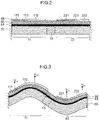
- Fig. 2 is a cross-sectional view taken along a line 2-2 in Fig. 1 .
- the cross-sectional view of a portion of the first actuator section 11 and the second actuator section 22 is illustrated, and the illustration of a portion of the first fixture member 51 and the second fixture member 52 is omitted.
- each of the first actuator section 11 and the second actuator section 22 is a unimorph type thin film piezoelectric actuator having a lamination structure in which a lower electrode 64, a piezoelectric body 66, and an upper electrode 68 are laminated in this order on a substrate of silicon (Si) that functions as a diaphragm 60.
- Si silicon
- the upper electrode 68 the first electrode section 111, the second electrode section 112, the third electrode section 221, and the fourth electrode section 222 are included.
- Each of the first actuator section 11 and the second actuator section 22 functions as a piezoelectric thin film unimorph actuator on which deflection deformation is performed in the up-down direction of Fig. 2 due to the inverse piezoelectric effect of the piezoelectric body 66 by applying voltage between the upper electrode 68 and the lower electrode 64 (see Fig. 3 ).
- the posture of "A” can be tiled, and "A” can be turned upside down, and even when the lamination direction of the lamination structure that depends on the posture of the substrate and the film is not always matched with the up-down direction using the gravity direction as a reference, the surface of a member that is a certain reference (for example, A) is set as a reference, and a direction that is away from the surface in the thickness direction is caused to correspond to "on" in order to represent the upper-lower relationship of the lamination structure without confusion.
- a certain reference for example, A
- the representation of "lamination of B on A” may correspond to a case in which one or plurality of layers lies between “A” and “B", and “B” is laminated on “A” through the one or plurality of layers instead of the case in which "B” is directly laminated on "A” so as to be in contact with "A".
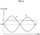
- Fig. 3 is a schematic cross-sectional view illustrating a state of deformation of the piezoelectric actuator section at the time of application of drive voltage.
- the drive voltages V 1 , and V 2 are described as drive voltages by waveforms of sine waves having opposite phases to each other (phase difference 180°) (see Fig. 4 ).
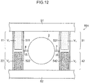
- Fig. 4 is a waveform diagram illustrating examples of the drive voltages V 1 and V 2 .
- V 1 and V 2 are voltages having the opposite phases to each other (phase difference 180°), and for an electrode group of the first electrode section 111 and the third electrode section 221, and an electrode group of the second electrode section 112 and the fourth electrode section 222, the voltages (V 1 , and V 2 ) having the opposite phases to each other are applied.
- V 1 and V 2 can be represented by as follows.
- V 1 V off1 + V 1A sin ⁇ t
- V 2 V off2 + V 2A sin ⁇ t + ⁇
- V 1A and V 2A are voltage amplitudes, and " ⁇ ” is an angular frequency, and “t” is a time, and “ ⁇ ” is a phase difference.
- the offset voltages V off1 and V off2 are optional, and for example, it is preferable that the drive voltages V 1 and V 2 are set so as not to exceed polarization inversion voltage of the piezoelectric body.
- each of the actuator sections (11, 22, 31, and 42) is driven by a resonant frequency that corresponds to the resonant mode in which tilting displacement occurs in the first torsion bar section 4 and the second torsion bar section 7 that supports the mirror section 2, large tilting displacement occurs in the first torsion bar section 4, the second torsion bar section 7, and the mirror section 2, so that a wide tilting angle range can be obtained. As a result, a wide range can be scanned.
- the piezoelectric body layer is not separated (divided) in a unit of the electrode section, and used as a single piezoelectric body film, but in the embodiment of the invention, the piezoelectric body 66 may also be divided correspondingly the division configuration of the electrode section.
- the portion of the piezoelectric body 66, which is sandwiched by the upper and lower electrodes functions as a driving force generation section or a stress detection section (sensor section), so that an unnecessary piezoelectric body portion that does not directly contribute to an operation as such a piezoelectric conversion section (piezoelectric element section) (portion in which there is no upper electrode) can be eliminated.
- the unnecessary piezoelectric body portion is eliminated and division of the piezoelectric body is performed in a unit of the piezoelectric conversion section, the rigidity of the actuator section is reduced, and the actuator section is deformed easily.
- Fig. 5 is a schematic diagram illustrating displacement of the piezoelectric body in each of the first actuator section 11 and the second actuator section 22 at the time of resonance driving.
- Fig. 6 is a schematic diagram illustrating a direction of a principal stress in each of the first actuator section 11 and the second actuator section 22 at the time of resonance driving.
- a portion illustrated by an arrow B in Fig. 5 is a portion that corresponds to the coupling section 15, and a state in which tilting displacement occurs in this portion is illustrated in Fig. 5 .
- the first actuator section 11 and the second actuator section 22 are in the bending deformation state illustrated in Figs. 5 and 6 in a driving state by the resonant mode vibration, there are generated a portion to which a stress in a compression direction (compression stress) is applied (reference numerals 71 and 73 in Fig.
- the stress described herein is a stress generated in the x-y plane when the film thickness direction is set as the z axis, a direction having the largest absolute value of the component from among principal stress vectors in the x-y plane is set as a direction of the stress.
- the first electrode section 111, the second electrode section 112, the third electrode section 221, and the fourth electrode section 222 are respectively arranged.
- the first electrode section 111 is provided for the compression stress area 71 in Fig. 5
- the second electrode section 112 is provide for the tensile stress area 72
- the third electrode section 221 is provided for the compression stress area 73
- the fourth electrode section 222 is provided for the tensile stress area 74.
- the insulation sections 113, 133, and 223 are formed so as to respectively correspond to the intermediate areas 76, 77, and 78.
- a parameter such as a device dimension, Young's modulus of a material, and a device shape is given, and analysis can be performed using a mode analysis method.
- stress distribution in the piezoelectric body at the driving by the resonant mode is analyzed, and division into the areas of the upper electrode is performed so as to correspond to the segmentation of the compression stress area and the tensile stress area in the stress distribution based on the analysis result, and the arrangement configuration of the first electrode section 111, the second electrode section 112, the third electrode section 221, and the fourth electrode section 222 is determined.
- the electrode sections can be divided into two groups.
- the first electrode section 111 and the third electrode section 221 belong to a first group (first electrode group), and the second electrode section 112 and the fourth electrode section 222 belong to a second group (second electrode group).
- drive voltage having the same phase is applied to the electrode sections that correspond to the areas having the same stress direction, and the drive voltages having different phases (optimally, the opposite phases to each other) are applied to the electrode sections that correspond to the areas having different stress directions (stresses having opposite directions), so that piezoelectric power can be converted into tilting displacement the most efficiently.
- the example is described above in which the drive voltage V 1 is applied to the first electrode section 111 and the third electrode section 221, and the drive voltage V 2 that has the opposite phase to the drive voltage V 1 is applied to the second electrode section 112 and the fourth electrode section 222, but the drive voltage V 2 can be applied to the first electrode section 111 and the third electrode section 221, and the drive voltage V 1 can be applied to the second electrode section 112 and the fourth electrode section 222.
- each of the electrode sections (111, 112, 221, and 222) is constituted by a single electrode
- at least one of the electrode sections (111, 112, 221, and 222) may be constituted by a plurality of electrodes.
- the fifth electrode section 311, and the sixth electrode section 312 of the third actuator section 31, and, the seventh electrode section 421, and the eighth electrode section 422 of the fourth actuator section 42 have arrangements that are respectively similar to the above-described electrode sections (111, 112, 221, and 222).
- Fig. 7 is a diagram illustrating an example in which all of the first electrode section 111 to the eighth electrode section 422 are used as driving electrodes.
- a portion in which the piezoelectric body 66 lies between each of the electrode sections (111, 112, 221, 222, 311, 312, 421, and 422) as the upper electrode 68 and the lower electrode 64 (see Fig. 2 ) operates as a piezoelectric element section.
- all of the electrode sections are used as driving electrodes, and all of the piezoelectric element sections function as driving force generation sections.
- the same drive voltage V 2 is applied to the electrode group of the first electrode section 111 of the first actuator section 11, the third electrode section 221 of the second actuator section 22, the fifth electrode section 311 of the third actuator section 31, and the seventh electrode section 421 of the fourth actuator section 42, and the drive voltage V 1 that has the opposite phase to the drive voltage V 2 is applied to the second electrode section 112 of the first actuator section 11, the fourth electrode section 222 of the second actuator section 22, the sixth electrode section 312 of the third actuator section 31, and the eighth electrode section 422 of the fourth actuator section 42.
- the piezoelectric element sections that respectively correspond to the electrode sections (111, 112, 221, 222, 31 1, 312, 421, and 422) are used as driving force generation sections, so that a large displacement angle can be obtained.
- phase difference 0° is not limited to "phase difference 0°”
- phase difference 180° includes an allowable range of a phase difference in which the phases are employed as substantially the opposite phase, which is not problematic in practice (for example, 180° ⁇ 10°).
- the voltage amplitude and phase difference of drive voltage that is applied to each of the piezoelectric element sections may be adjusted as appropriate in order to adjust operation performance between elements.
- the embodiment of the presently disclosed subject matter includes a case in which voltage amplitude and a phase difference are changed within the range of such adjustment.
- Fig. 8 is a diagram illustrating an example in which a part of the first electrode section 111 to the eighth electrode section 422 is used as a sensing (detection) electrode for stress detection.
- the fourth electrode section 222 and the eighth electrode section 422 are used as detection electrodes, and the other electrode sections are used as driving electrodes.
- the detection electrode is set at a floating potential and detects voltage that is generated by a piezoelectric effect of the piezoelectric body 66 (positive piezoelectric effect).
- electrodes represented by "s" are detection electrodes that are used to detect a sensing signal and are set at a floating potential.
- the voltage detection section functions as a stress detection section.
- a drive circuit that enables keeping of the resonant state, etc. can be configured.
- Fig. 9 is a diagram illustrating an example of a configuration in which at least one voltage detection section is provided in each of the actuator sections (11, 22, 31, and 42) that constitutes the piezoelectric actuator section.
- the first electrode section 111, the fourth electrode section 222, the fifth electrode section 311, and the eighth electrode section 422 function as sensing electrodes.
- the operation state can be grasped for each of the actuator sections, so that application control of drive voltage can be performed appropriately based on a detection signal, and further stable resonance driving can be achieved.
- Fig. 10 is a modification of Fig. 8 .
- Fig. 10 is diagram illustrating an example in which each of the fourth electrode section 222 and the eighth electrode section 422 described in Fig. 8 is further divided into a plurality of electrodes.
- Fig. 10 an example is illustrated in which the fourth electrode section 222 is divided into three electrodes 222A, 222B, and 222C in the x direction, and the eighth electrode section 422 is divided into three electrode 422A, 422B, and 422C in the x direction.
- the electrode 222B that is arranged at the center is set at a floating potential and used as a voltage detection section (sensing electrode), and the remaining electrodes 222A and 222C (left and right sides of the electrode 222B) are used as drive voltage application sections (that is, driving force generation section).
- the electrode 422B that is arranged in the center is set at a floating potential and used as a voltage detection section (sensing electrode), and the remaining electrodes 422A and 422C that are arranged on the left and right sides of the electrode 422B are used as drive voltage application sections (that is, driving force generation sections).
- an electrode area that is used for the voltage detection section is minimized, and a high scan angle is kept, and stress detection can be performed.
- Fig. 11 is a modification of Fig. 9 .
- Fig. 11 an example is described in which each of the first electrode section 111, the fourth electrode section 222, the fifth electrode section 311, and the eighth electrode section 422 illustrated in Fig. 9 is further divided into a plurality of electrodes.
- the same reference numerals is assigned to an element that is similar to that of the structure described in Fig. 10 , and the description is omitted herein.
- Fig. 11 an example is illustrated in which the first electrode section 111 is divided into three electrodes 111A, 111B, and 111C in the x direction, and the fourth electrode section 222 is divided into three electrodes 222A, 222B, and 222C in the x direction, and the fifth electrode section 311 is divided into three electrodes 311A, 311B, and 311C in the x direction, and the eighth electrode section 422 is divided into three electrodes 422A, 422B, and 422C in the x direction.
- the electrode 111B that is arranged at the center is set at a floating potential and used as a voltage detection section (sensing electrode), and the remaining electrodes 111A and 111C (left and right sides of the electrode 11 1B) are used as drive voltage application sections (that is, driving force generation sections).
- the electrode 311B that is arranged at the center is set at a floating potential and used as a voltage detection section (sensing electrode), and the remaining electrodes 311A and 311C that are arranged on the left and right sides of the electrode 311B are used as drive voltage application sections (that is, driving force generation sections).
- an electrode area that is used for the voltage detection section is minimized, and a high scan angle is kept, and the stress detection can be performed.
- a micro scanner device is manufactured by a manufacturing method that is described below as the first embodiment.
- a Ti layer is formed by 30 nm, and a Ir layer is formed by 150 nm on a Silicon On Insulator (SOI) substrate having a lamination structure in which a handle layer 350 ⁇ m, a box layer 1 ⁇ m, and a device layer 24 ⁇ m are laminated by a sputtering method at substrate temperature 350°C.
- a conductive layer by the lamination body of the Ti layer (30 nm) and the Ir layer (150 nm) corresponds to "the lower electrode 64" described in Fig. 2 .
- Film-forming of the piezoelectric body (PZT) layer by 2.5 ⁇ m is performed on the substrate that is formed so as to laminated with the lower electrode (Ti/Ir) in the procedure 1, using a high frequency (radio frequency: RF) sputtering device.
- RF radio frequency
- film-forming gas a mixture gas of 97.5% Ar and 2.5% O 2 is used, and as a target material, the composition of Pb 1.3 ((Zr 0.52 Ti 0.48 ) 0.88 Nb 0.12 ) O 3 is used.
- Film-forming pressure is 2.2 mTorr (about 0.293 Pa), and film-forming temperature is 450°C.
- the obtained PZT layer is a Nb dope PZT thin film to which 12% of Nb is doped in the atomic composition ratio.
- a composition ratio of Pb contained in the formed PZT thin film was measured by the X-ray Fluorescence Analysis (XRF).
- XRF X-ray Fluorescence Analysis
- a measured ratio of Pb / (Zr + Ti + Nb) was 1.05.
- a ratio "a" of a Pb amount contained in the formed PZT thin film having a perovskite structure may be unequal to 1.00, due to an interstitial atom or lattice defect.
- a ratio "c" of O atoms contained in the formed PZT thin film having a perovskite structure may be unequal to 3.00, due to an interstitial atom or lattice defect.
- Pattern forming of an upper electrode having a lamination structure of Pt/Ti by a liftoff method is performed on the substrate on which the PZT layer is formed by the procedure 2, and pattern etching of the PZT thin film is performed by inductively coupled plasma (ICP) dry etching.
- ICP inductively coupled plasma
- pattern etching is performed on a device layer by a dry etch process of silicon, and the shapes of the actuator section, the mirror section, and the fixture member are processed.
- Deep etching (Deep RIE: Reactive Ion Etching) of a handle layer is performed on the back surface of the substrate.
- a micro scanner device having the structure as illustrated in Fig. 1 is manufactured.
- the film-forming of a PZT thin film is performed directly on a substrate by the sputtering method, and then the dry etching process is performed so as to form the PZT thin film.
- the piezoelectric body is thinned to simplify the manufacturing process, and fine patterning can be performed. This improves yield significantly, and the further downsizing of the device can be achieved.
- the piezoelectric body of the actuator section is not limited to the thin film piezoelectric body, and a unimorph actuator may be formed by attaching a bulk piezoelectric body to a diaphragm, and a bimorph actuator may be formed by attaching piezoelectric bodies having two different polarities.
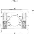
- a micro scanner device By using the substrate (SOI substrate) and the manufacturing process method that are completely the same as the first embodiment, a micro scanner device according to a comparative example 1 illustrated in Fig. 12 is manufactured.
- a device 501 illustrated in Fig. 12 the same reference numeral is assigned to an element that is the same as or similar to the structure of Fig. 1 , and the description is omitted herein.
- the upper electrodes of the first actuator section 11, the second actuator section 22, the third actuator section 31, and the fourth actuator section 42 respectively include only single electrode sections 511, 522, 531, and 542.
- Fig. 12 is a diagram illustrating an example in which all of the electrode sections (511, 522, 531, and 542) are used as driving electrodes.
- the drive voltage V 1 is applied to the electrode section 511 of the first actuator section 11 and the electrode section 531 of the third actuator section 31, and the drive voltage V 2 having an opposite phase to the drive voltage V 1 is applied to the electrode section 522 of the second actuator section 22 and the electrode section 542 of the fourth actuator section 42.
- one of the plurality of electrode sections (511, 522, 531, and 542) is used as a detection (sensing) electrode.
- One of the first actuator section 11 and the second actuator section 22 that are connected to the first torsion bar section 4 is caused to function as a sensing electrode.
- one of the third actuator section 31 and the fourth actuator section 42 that are connected to the second torsion bar section 7 is caused to function as a sensing electrode.
- Fig. 13 an example is illustrated in which the electrode sections 511 and 531 are used as sensing electrodes in view of the symmetry.
- the electrode section that is used for sensing is set at a floating potential and detects voltage that is generated by the positive piezoelectric effect of the piezoelectric body.
- Fig. 14 is a graph illustrating a relationship between drive voltage and a scan angle in a device that is an experiment target.
- first embodiment corresponds to the configuration in Fig. 7
- first embodiment (sensing is performed) corresponds to the configuration in Fig. 8
- comparativative example 1 corresponds to the configuration in Fig. 12
- comparativative example 1 (sensing is performed) corresponds to the configuration in Fig. 13 .
- the drive voltages V 1 , and V 2 by the sine wave of voltage amplitude V PP are input to the drive electrode section, resonant vibration that is associated with the rotation movement of the mirror section 2 is induced, and a machine deflection angle of the mirror section 2 is measured by a scan angle of laser.
- the devices according to "first embodiment” and “first embodiment (sensing is performed)" are applied correspondingly to the descriptions in Figs. 7 and 8 .
- the devices according to "comparative example 1" and “comparative example 1 (sensing is performed)” are applied correspondingly to the descriptions in Figs. 12 and 13 .
- the resonant frequency is 25 kHz.
- Fig. 14 The result of the experiment is illustrated in Fig. 14 .
- the horizontal axis indicates voltage amplitude (unit of volts [V]), and the vertical axis indicates an optical scan angle (unit of degrees [deg]).
- the device according to the first embodiment in which a single actuator section includes a plurality of electrodes section can obtain a high scan angle as compared with the device according to the comparative example 1.
- a high scan angle can be kept as compared with the device according to the comparative example 1.
- A is an element of A-site, and at least one element including Pb.
- the standard molar ratio of the A-site element, the B-site element, and the oxygen element is 1:1:3, and the molar ratio may be deviated from the standard molar ratio within a range in which the perovskite structure can be obtained.
- the perovskite-type oxide that is represented by the above-described general formula (P) there are a lead-containing compound such as lead titanate, lead zirconate titanate (PZT), lead zirconate, lead lanthanum titanate, lead lanthanum zirconate titanate, magnesium niobate lead zirconium titanate, nickel niobate zirconium lead titanate, zinc niobate zirconium lead titanate, and mixed crystal systems of the compounds, and a non-lead-containing compound such as barium titanate, strontium barium titanate, bismuth sodium titanate, bismuth potassium titanate, sodium niobate, potassium niobate, lithium niobate, bismuth ferrite, and mixed crystal systems of the compounds.
- a lead-containing compound such as lead titanate, lead zirconate titanate (PZT), lead zirconate, lead lanthanum titanate, lead lanthanum zir
- the piezoelectric body film according to the embodiment includes one or more kinds of perovskite-type oxides (PX) that are represented by the following formula.
- PX perovskite-type oxides
- A is an element of A-site, and at least one element including Pb.
- the perovskite-type oxide (PX) is a genuine PZT, or an oxide that is obtained by replacing a part of B-site of the PZT with M.
- PZT that is doped with various donor ions having a valence that is higher than the valence of a replacement ion, it is known that a characteristic of the piezoelectric performance, etc. is improved as compared with the genuine PZT.
- M is one or more types of donor ions the valence of which is larger than that of tetravalent Zr and Ti.
- a donor ion there are V 5+ , Nb 5+ , Ta 5+ , Sb 5 +, Mo 6+ , W 6+ , etc.
- the b-x-y is not particularly limited as long as the range is a range in which the perovskite structure can be obtained.
- M is Nb
- the Nb/(Zr+Ti+Nb) molar ratio is 0.05 or more to 0.25 or less, and it is further preferable that the molar ratio is 0.06 or more to 0.20 or less.
- the piezoelectric body film that is constituted by the perovskite-type oxide that is represented by the above-described general formulas (P) and (PX) has a high piezoelectric distortion constant (d31 constant), so that a piezoelectric actuator that includes such a piezoelectric body film has an excellent displacement characteristic.
- the piezoelectric actuator that includes the piezoelectric body film that is constituted by the perovskite-type oxide that is represented by the general formula (P) and (PX) has a voltage-displacement characteristic of excellent linearity.
- the piezoelectric material has an actuator characteristic and a sensor characteristic that are excellent for the embodiments of the presently disclosed subject matter. It is noted that the perovskite-type oxide that is represented by the general formula (PX) has a higher piezoelectric constant than the perovskite-type oxide that is represented by the general formula (P).
- a lead zirconate titanate (PZT) thin film that is doped with Nb by 12% in atomic composition percentage can be used.
- PZT lead zirconate titanate
- the PZT is selected as the piezoelectric body material that is used for the actuator section (driving force generation section and stress detection section), but the embodiment is not limited to such a material.
- a lead-free piezoelectric body of BaTiO 3 , KNaNbO 3 , BiFeO 3 , etc. can be used, and a non-perovskite piezoelectric body of AlN, ZnO 2 , etc. can be also used.
- a vapor-phase growth method As a film-forming method of the piezoelectric body, a vapor-phase growth method is preferable. For example, instead of the sputtering method, various methods such as an ion plating method, a metal organic chemical vapor deposition method (MOCVD), a pulse laser deposition (PLD) method can be applied. In addition, it is conceivable that a method other than the vapor-phase growth method (for example, sol-gel method, etc.) is used. It is preferable that film-forming of a piezoelectric thin film is directly performed on a substrate by the vapor-phase growth method, the sol-gel method, etc. In particular, as the piezoelectric body 66 according to the embodiment, it is preferable that a thin film has a film thickness of 1 ⁇ m or more to 10 ⁇ m or less.
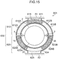
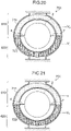
- a micro scanner device 601 illustrated in Fig. 15 is manufactured using completely the same substrate (SOI substrate) as the first embodiment by the same process method.
- the same reference numeral is assigned to an element that is the same as or similar to the device 1 illustrated in Fig. 1 , and the description is omitted herein.
- the micro scanner device 601 is constituted by a first actuator section 610 and a second actuator section 620 that are tuning-fork type unimorph actuators, and the micro scanner device 601 has an approximately annular actuator shape in a plan view by the structure in which the first actuator section 610 and the second actuator section 620 are coupled to each other.
- an oval annular appearance (contour) shape that is slightly flattened from a perfect circle is illustrated, but the annular actuator shape is not limited to the illustrated example.
- An annular shape of a perfect circle may be employed, and an oval annular shape the aspect ratio of which is further larger than the example of Fig. 15 may be employed.
- large torque can be obtained by a large area of the actuator section, so that the oval shape is preferable as compared with the perfect circle.
- the first torsion bar section 4 is connected to the coupling section 15, and the second torsion bar section 7 is connected to the coupling section 35.
- the first actuator section 610 has a tuning-fork shape in which two arm sections 610A and 610B are arranged so as to be divided on both sides of the x direction of the mirror section 2.
- a base end section 615 that corresponds to a root portion that bifurcates toward the two arm sections 610A and 610B is fixed to the first fixture member 51.
- the first actuator section 610 operates as tuning-fork type piezoelectric actuator that uses the base end section 615 that is fixed to the first fixture member 51 as a fixture end.
- the upper electrode of the first actuator section 610 is divided into a single first electrode section 611 and two second electrode sections 612A and 612B for the longitudinal direction along the shapes of the arm sections 610A and 610B.
- the structure of the second actuator section 620 is similar to the structure of the first actuator section 610.
- the second actuator section 620 has a tuning-fork shape in which two arm sections 620A and 620B are arranged so as to be divided on both sides of the x direction of the mirror section 2.
- a base end section 625 that corresponds to a root portion that bifurcates toward the two arm sections 620A and 620B is fixed to the second fixture member 52, and operates as a tuning-fork-shaped piezoelectric actuator that uses the base end section 625 as a fixture end.
- the upper electrode of the second actuator section 620 is divided into two third electrode sections 623A and 623B, and a single fourth electrode section 624 along the shapes of the arm sections 620A and 620B.
- a piezoelectric actuator section 630 is configured that has an annular structure in which the arm sections 610A and 610B of the first actuator section 610 are respectively connected to the arm sections 620A and 620B of the second actuator section 620 through the coupling sections 15 and 35.
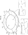
- Fig. 16 is a schematic perspective view illustrating deformation of the piezoelectric actuator section and distribution of stress directions of principal stresses at the time of resonant mode driving of the micro scanner.
- the mirror section 2, the first torsion bar section 4, and the second torsion bar section 7 illustrated in Fig. 15 are omitted.
- portions that are indicated by arrows B are portions that correspond to the coupling sections 15 and 35.
- the piezoelectric actuator section 630 is deformed as illustrated in Fig. 16 , and tilting displacement occurs in the portions that are indicated by the arrows B.
- tilting displacement of the first torsion bar section 4, the second torsion bar section 7 and the mirror section 2 illustrated in Fig. 15 is induced.
- the first electrode section 611, the second electrode sections 612A and 612B, the third electrode sections 623A and 623B, and the fourth electrode section 624 are respectively arranged for the areas of the piezoelectric body section having different stress directions (reference numerals 81, 82A, 82B, 83A, 83B, and 84).
- Electrode group When a group (electrode group) is constituted by electrode sections that correspond to the areas having the same stress direction, and the piezoelectric conversion sections are segmented into two groups so as to correspond to areas in which stresses occurs in opposite directions to each other, the first electrode section 611, and the third electrode sections 623A and 623B belong to a first group (first electrode group), and the second electrode sections 612A and 612B, and the fourth electrode section 624 belong to a second group (second electrode group).
- piezoelectric power can converted into tilting displacement the most efficiently.
- compression stress and tensile stress are defined by selecting two principal stresses in the plane that is orthogonal to the film thickness direction of the piezoelectric body, from three principal stress vector that are orthogonal to each other ( ⁇ 1 and ⁇ 2 in Fig. 16 ), and selecting a direction having a larger absolute value (direction of the maximum principal stress) from the selected two principal stresses.
- the direction is the direction of ⁇ 2 in Fig. 16 .
- a vector in a direction toward the outside is defined as the tensile direction
- a vector in a direction toward the inside is defined as the compression direction.
- the definition is performed as described above is that the dimensions of the actuator section is generally planar (length of height is small enough as compared with the dimension in the plane direction) in the piezoelectric MEMS device, and the stress ⁇ 3 in the film thickness direction can be regarded as nearly zero.
- stresses in the opposite directions to each other is determined based on the above-described definition.
- all of the electrode sections can be used for driving, or a part of electrode sections can be used for sensing (detection).
- Fig. 17 is a diagram illustrating an example in which all of the electrode sections are used as drive electrodes.
- the drive voltage V 1 is applied to the first electrode section 611, and the third electrode sections 623A and 623B that belong to the first group, and the drive voltage V 2 having the opposite phase as the drive voltage V 1 is applied to the second electrode sections 612A and 612B, and the fourth electrode section 624 that belong to the second group.
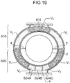
- Fig. 18 is a diagram illustrating an example in which a part of electrode sections is used as a sensor.
- an example is illustrated in which the fourth electrode section 624 in the second actuator section 620 is used as a sensing electrode.
- Fig. 19 is a modification of Fig. 18 , and illustrates an example in which the fourth electrode section 624 in Fig. 18 is divided into a plurality of electrodes 624A, 624B, and 624C, and the electrode 624B out of the plurality of electrodes 624A, 624B, and 624C is used as a sensor.
- first electrode section 611 of the first actuator section 610 is used as a sensor (not illustrated).
- first electrode section 611 can have a similar structure to the fourth electrode section 624 described in Figs. 18 and 19 .
- a micro scanner device according to a comparative example 2 as illustrated in Fig. 20 is manufactured using a substrate (SOI substrate) and a manufacturing process method that are completely the same as the first embodiment.
- a device 701 illustrated in Fig. 20 the same reference numeral is assigned to an element that is the same as or similar to the structure of Fig. 15 , and the description is omitted herein.
- the device 701 according to the comparative example 2 has a structure in which the upper electrodes of the first actuator section 610 and the second actuator section 620 only respectively include single electrode sections 711 and 722.
- Fig. 20 is a diagram illustrating an example in which the two electrode sections 711 and 722 are used as driving electrodes.
- the drive voltage V 2 can be applied to the electrode section 711 of the first actuator section 610, and the drive voltage V 1 that has the opposite phase to the drive voltage V 2 can be applied to the electrode section 722 of the second actuator section 620.
- one of the two electrode sections 711 and 722 is used for detection (sensing) as illustrated in Fig. 21 .
- Fig. 21 an example is illustrated in which the first electrode section 711 of the first actuator section 610 is used for sensing.
- the electrode section that is used for sensing is set at a floating potential, and detects voltage that is generated by the positive piezoelectric effect of the piezoelectric body.
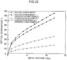
- Fig. 22 is a graph illustrating a relationship between drive voltage and a scan angle in a device that is an experiment target.
- second embodiment corresponds to the configuration of Fig. 17
- second embodiment (sensing is performed) corresponds to the configuration of Fig. 18
- comparativative example 2 corresponds to the configuration of Fig. 20
- comparativative example 2 (sensing is performed) corresponds to the configuration of Fig. 21 .
- the drive voltages V 1 , and V 2 by the sine wave of the voltage amplitude V PP are input to the driving electrode section, and resonant vibration that is associated with a rotation movement of the mirror section 2 (oscillating movement in which rotation is performed around the rotating axis R A ) is induced, and a machine deflection angle of the mirror section 2 is measured by a scan angle of laser.
- the devices according to "second embodiment” and “second embodiment (sensing is performed)" are applied correspondingly to the descriptions of Figs. 17 and 18 .
- the resonant frequency is 26 kHz.
- Fig. 22 The result of the experiment is illustrated in Fig. 22 .
- the horizontal axis indicates voltage amplitude (unit of volts [V]), and the vertical axis indicates an optical scan angle (unit of degrees [deg]).
- the device according to the second embodiment using the tuning-fork type actuator obtains a higher scan angle than the device according to the first embodiment using the cantilever type actuator.
- the device according to the second embodiment in which the plurality of electrodes sections are included in the single actuator section obtains a higher scan angle than the device according to the comparative example 2.
- the device according to the second embodiment (“second embodiment in which sensing is performed") keeps a higher scan angle than the device according to the comparative example 2.
- a component noise vibration
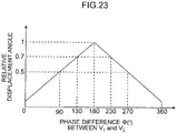
- a relationship between a phase difference and a relative displacement angle between the drive voltages of V 1 and V 2 a relationship between a phase difference and a relative displacement angle between the drive voltages of V 1 and V 2 .
- the displacement angle becomes maximum when a phase difference between the drive voltages V 1 and V 2 is 180° (opposite phases to each other) and becomes minimum when the phase difference is 0° (same phase).
- the range of a phase difference is caused to be within a range of "90° ⁇ 270°" in order to obtain an enough displacement angle.
- the phase difference is caused to be within a range of "130° ⁇ 230°".
- the number of types of the drive waveforms may be two or more.
- drive voltage that is applied to the first electrode section 611 can be set at "V 11 "
- drive voltage that is applied to the second electrode sections 612A and 612B can be set at "V 12 "
- drive voltage that is applied to the third electrode sections 623A and 623B can be set at "V 21 "
- drive voltage that is applied to the fourth electrode section 624 can be set at "V 22 ".
- V 11 V off11 + V 11A sin ⁇ t
- V 12 V off12 + V 12A sin ⁇ t + ⁇
- V 21 V off21 + V 21A sin ⁇ t
- V 22 V off22 + V 22A sin ⁇ t + ⁇
- V 11A “, “V 12A “, “V 21A “, and “V 22A” are voltage amplitudes, and " ⁇ ” is an angular frequency, and “t” is a time, and “ ⁇ ” is a phase difference.
- the phase difference ⁇ is in a range of "90° ⁇ 270°", and more preferably, in a range of "130° ⁇ 230°".
- V 11A “, “V 12A “, “V 21A “, and “V 22A” a given value of 0 or more can be obtained.
- V 11A ,” “V 12A “, “V 21A “, and “V 22A “ different values can be set, and the same value can be set to a part or all of “V 11A ,” “V 12A “, “V 21A “, and “V 22A “.
- the phases of "V 11 “ and “V 21 “ are matched with each other, and the phases of "V 12 “ and “V 22 " may be matched with each other but not completely, and a slight phase shift of about ⁇ 10° is permissible.
- the applied voltage is not limited to a sine wave, and a cycle waveform such as a square wave and a triangle wave can be applied.
- the devices according to the first embodiment and the second embodiment can obtain a high displacement amount even when driving in the non-resonant mode is performed. That is, driving can be performed even with a frequency that is low enough as compared with a resonant frequency without usage of resonant.
- Fig. 25 is a graph illustrating an experiment result of measurement of a displacement angle when driving is performed by applying DC voltage (at the time of non-resonance driving) for the devices according to the second embodiment and the comparative example 2.
- the horizontal axis indicates drive voltage, and the vertical axis indicates an optical scan angle.
- Fig. 25 illustrates a displacement angle when a voltage waveform (square wave) of 1 kHz is applied for the structure in the second embodiment and the comparative example 2. In this experiment, offset voltage is applied so as not to exceed a coercive field of the piezoelectric body.
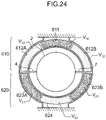
- a specific example of each of the dimensions in the second embodiment is illustrated in Fig. 26 .
- the whole length "a" is 2.3 mm
- the width "b" of the arm section of the actuator is 0.4 mm
- the diameter "c” of the mirror section is 1.2 mm
- the horizontal width "d” between the coupling sections of the torsion bar section is 1.7 mm
- the thickness "e” of the torsion bar section is 0.16 mm.
- Fig. 27 is a diagram illustrating a structure example of a control system that is used for driving of the device.
- a control system of the device configuration according to the second embodiment illustrated in Fig. 18 is illustrated.
- each of the first electrode section 611, and the second electrode sections 612A and 612B of the first actuator section 610, and the third electrode sections 623A and 623B of the second actuator section 620, which are used for driving is connected to a corresponding voltage output terminal in the drive circuit 810.
- the drive voltage V 1 is supplied to the first electrode section 611 of the first actuator section 610 and the third electrode sections 623A and 623B of the second actuator section 620 from the drive circuit 810.
- the drive voltage V 2 is supplied to the second electrode sections 612A and 612B of the first actuator section 610 from the drive circuit 810. It is noted that, in Fig. 27 , the electrode sections to which the same drive voltage is applied are connected to each other in parallel, but individual drive voltage may be supplied to each of the electrode sections.
- the drive circuit 810 supplies the drive voltages V 1 and V 2 that are used to cause the mirror section 2 to perform resonance driving in the vicinity of a resonant frequency fx of the resonant mode in which the mirror section 2 performs the rotation movement around the rotating axis R A .
- the fourth electrode section 624 of the second actuator section 620 which is used for sensing, is connected to a detection circuit 812.
- the lower electrode 64 is connected to a shared terminal of the drive circuit 810 and the detection circuit 812 (V 0 terminal, for example, a GND terminal).
- Each of the electrodes is connected to the drive circuit 810 or the detection circuit 812 through a pattern wiring section or a wiring member such as wire bonding on the substrate, which is not illustrated.
- a voltage signal is detected from the fourth electrode section 624 through the detection circuit 812, and the detection result is notified to a control circuit 814.
- the control circuit 814 transmits a control signal to the drive circuit 810 so as to keep the resonance based on the signal that is transmitted from the detection circuit 812, and controls application of drive voltage to the first actuator section 610 and the second actuator section 620.
- feedback to the drive circuit 810 is performed so that the phase of the waveform of the drive voltage that is applied to the piezoelectric actuator section and the phase of the waveform that is detected from the stress detection section (sensor section) become a certain value to keep the resonance.
- the control circuit 814 controls voltage that is applied to the piezoelectric actuator section or a drive frequency based on the detection signal that is obtained from the stress detection section.
- Such a feedback control circuit can be incorporated into the detection circuit 812.
- the drive circuit 810, the detection circuit 812, and the control circuit 814 can be configured together as an integrated circuit such as an application specific integrated circuit (ASIC).
- ASIC application specific integrated circuit
- the structure is employed in which division of the electrode of the actuator section is performed based on stress distribution of principal stresses at the time of resonant mode vibration, which is grasped from simulation analysis of the device correspondingly to the compression direction area and the tensile direction area in which the stress directions are opposite directions to each other, and by providing the electrode section of the first group and the electrode section of the second group in which driving forces having different phases are generated, driving can be performed efficiently, and a high displacement angle can be obtained.
- the actuator section can be used as the stress detection section that detects a potential as which a part or all of the electrodes that constitute one of electrode sections are set as a floating potential.
- the stress detection section cannot generate driving force, but still can keep a high scan angle as compared with the structure in the related art.
- the first torsion bar section 4 and the second torsion bar section 7 are connected to a portion that is to be matched with the rotating axis R A of the mirror section 2, and extend in the axial direction of the rotating axis R A toward the outside of the mirror section 2.
- the example is described above in which the first torsion bar section 4 and the second torsion bar section 7 are connected to the position that is matched with the rotating axis R A of the mirror section 2, but the connection position of the torsion bar section may not be strictly matched with the rotating axis R A , and is not limited to the configuration of one connection position, and a plurality of connection positions may be employed.
- the rotating axis R A when an approximately center portion in the longitudinal direction of the mirror section 2 (true center point on the design and the surrounding and neighborhood of the center point) is the rotating axis R A , in addition to the configuration in which the torsion bar is supported so as to be connected to one position that is approximately matched with the rotating axis R A and, a configuration can be employed in which the torsion bar is connected to two locations or more so as to have axis symmetry across the position of the rotating axis R A in a range that is approximately regarded as the center portion.
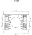
- Fig. 28 illustrates an example not falling under the scope of claim 1 in which torsion bar sections 4A, 4B, 7A, and 7B each two of which are located on one side are provided instead of the first torsion bar section 4 and the second torsion bar section 7 in Fig. 1 .
- the same reference numeral is assigned to an element that is the same as or similar to the structure illustrated in Fig. 1 , and the description is omitted herein.
- Fig. 1 the structure is described above the first torsion bar section 4 is connected to the coupling section 15 in which the first actuator section 11 is coupled to the second actuator section 22, but a configuration can be employed in which the first actuator section 11 and the second actuator section 22 are separated.
- Fig. 29 illustrates such an example.
- the same reference numeral is assigned to a member that is the same as or similar to the structure Figs. 1 and 28 , and the description is omitted herein.
- the first actuator section 11 and the second actuator section 22 are configured as cantilever structures so as to be independent of each other, and the torsion bar section 4A is connected to the distal end of the first actuator section 11, and the torsion bar section 4B is connected to the distal end of the second actuator section 22.
- the third actuator section 31 and the fourth actuator section 42 are configured as the cantilever structures so as to be independent of each other, and the torsion bar section 7A is connected to the distal end of the third actuator section 31, and the torsion bar section 7B is connected to the distal end of the fourth actuator section 42.
- mirror driving that is similar to that of Figs. 1 and 28 can be performed.
- the mirror drive device can be used for various purposes as an optical device that reflects light such as laser light and changes a traveling direction of the light.
- the mirror drive device can be widely applied to an optical deflector, an optical scanning device, a laser printer, a bar code reader, a display device, various optical sensors (distance measuring sensor and shape measurement sensor), an optical communication device, a laser projector, an optical interference tomographic image diagnostic apparatus, etc.
Claims (14)
- Dispositif d'entraînement de miroir (1) comprenant :une section de miroir (2) qui inclut une surface réfléchissante configurée pour réfléchir de la lumière ;une section de support de miroir (4, 7) qui est couplée à la section de miroir, la section de support de miroir étant configurée pour supporter la section de miroir de sorte que la section de miroir pivote autour d'un axe de rotation ;une section d'actionneur piézoélectrique (610, 620) qui est couplée à la section de support de miroir, la section d'actionneur piézoélectrique étant configurée pour générer une force d'entraînement qui amène la section de miroir à pivoter autour de l'axe de rotation ; etune section d'installation (51, 52) configurée pour supporter la section d'actionneur piézoélectrique,dans lequel : la section d'actionneur piézoélectrique inclut une première section d'actionneur (610) et une seconde section d'actionneur (620) qui sont déformées par un effet piézoélectrique inverse obtenu en appliquant une tension d'entraînement,la première section d'actionneur est agencée sur un côté de côtés qui prennent en sandwich la section de support de miroir, et la seconde section d'actionneur est agencée sur un autre côté de ceux-ci,une première section d'extrémité de base (11B, 31B) sur un côté opposé à la section de support de miroir dans la première section d'actionneur et une seconde section d'extrémité de base (22B, 42B) sur un côté opposé à la section de support de miroir dans la seconde section d'actionneur sont fixées à la section d'installation,le dispositif d'entraînement de miroir (1) est agencé de sorte qu'un entraînement d'inclinaison puisse se produire dans la section de support de miroir en pliant la première section d'actionneur et la seconde section d'actionneur dans des directions opposées l'une à l'autre,l'électrode supérieure de la première section d'actionneur inclut une première section d'électrode et une deuxième section d'électrode dont chacune est constituée par une ou une pluralité d'électrodes,l'électrode supérieure de la seconde section d'actionneur inclut une troisième section d'électrode et une quatrième section d'électrode dont chacune est constituée par une ou une pluralité d'électrodes,une configuration d'agencement de la première section d'électrode, la deuxième section d'électrode, la troisième section d'électrode et la quatrième section d'électrode correspond à une distribution de contraintes de contraintes principales dans une direction dans le plan qui est perpendiculaire à une direction d'épaisseur de couche du corps piézoélectrique dans une vibration de mode de résonance qui est associée au déplacement d'inclinaison de la section de miroir dû à la rotation autour de l'axe de rotation,dans une portion de corps piézoélectrique qui correspond à des positions de la première section d'électrode et de la troisième section d'électrode, et une portion de corps piézoélectrique qui correspond à des positions de la deuxième section d'électrode et de la quatrième section d'électrode, des contraintes présentant des directions opposées les unes aux autres sont générées dans une vibration du mode de résonance,et la première section d'actionneur et la seconde section d'actionneur sont des sections d'actionneur présentant une forme de type diapason dans laquelle deux sections de bras qui sont agencées de manière à être divisées sur les deux côtés des sections de miroir sont fournies,caractérisé en ce quedans la seconde section d'actionneur (620), une de la troisième et de la quatrième sections d'électrode est divisée en trois électrodes (624A, 624B, 624C), un des électrodes étant utilisée comme un capteur de manière à détecter une tension qui est générée par un effet piézoélectrique de la portion de corps piézoélectrique associé à une déformation de la portion de corps piézoélectrique, et les deux autres des trois électrodes (624A, 624B, 624C) sont utilisées comme des sections de génération de force d'entraînement.
- Dispositif d'entraînement de miroir (1) selon la revendication 1,dans lequel la première section d'actionneur et la seconde section d'actionneur sont raccordées l'une à l'autre, etla section de support de miroir est couplée à une section de couplage de la première section d'actionneur et de la seconde section d'actionneur.
- Dispositif d'entraînement de miroir (1) selon la revendication 1 ou 2,
dans lequel la première section d'actionneur et la seconde section d'actionneur sont des actionneurs monomorphes piézoélectriques et présentent des structures de laminage dans lesquelles un diaphragme, une électrode inférieure, un corps piézoélectrique, et une électrode supérieure sont laminés dans cet ordre. - Dispositif d'entraînement de miroir (1) selon l'une quelconque des revendications 1 à 3, comprenant en outre
une première section de support de miroir (4) et une seconde section de support de miroir (7) qui supportent la section de miroir depuis les deux côtés de l'axe de rotation dans une direction axiale, en tant que la section de support de miroir. - Dispositif d'entraînement de miroir (1) selon l'une quelconque des revendications 1 à 4,
dans lequel la première section d'actionneur et la seconde section d'actionneur incluent des structures de cantilever dans lesquelles la première section d'extrémité de base et la seconde section d'extrémité de base qui sont fixées par la section d'installation sont utilisées comme des extrémités d'installation. - Dispositif d'entraînement de miroir (1) selon l'une quelconque des revendications 1 à 5, comprenant en outre :un circuit d'entraînement (810) configuré pour fournir une tension d'entraînement à une électrode qui est incluse dans au moins une de la première section d'électrode et de la troisième section d'électrode, et fournir une tension d'entraînement à une électrode qui est incluse dans au moins une de la deuxième section d'électrode et de la quatrième section d'électrode,dans lequel une différence de phase ϕ entre la tension d'entraînement qui est appliquée à au moins une de la première section d'électrode et de la troisième section d'électrode et la tension d'entraînement qui est appliquée à au moins une de la deuxième section d'électrode et de la quatrième section d'électrode est dans une plage de « 130° ≤ ϕ ≤ 230° ».
- Dispositif d'entraînement de miroir (1) selon l'une quelconque des revendications 1 à 6, dans lequel :l'une (624B) des trois électrodes (624A, 624B, 624C) est définie comme un potentiel flottant ; etle dispositif d'entraînement de miroir (1) comprend en outre un circuit de détection configuré pour détecter la tension qui est générée par l'effet piézoélectrique qui est associé à la déformation de la seconde section d'actionneur (620), depuis l'une (624B) des électrodes (624A, 624B, 624C).
- Dispositif d'entraînement de miroir (1) selon l'une quelconque des revendications 1 à 7, comprenant en outre :
un circuit d'entraînement (810) configuré pour fournir une tension d'entraînement à la section d'actionneur piézoélectrique, et fournir une tension d'entraînement qui amène un entraînement de résonance à être effectué sur la section de miroir proche d'une fréquence de résonance fx du mode de résonance dans lequel la section de miroir effectue un mouvement de rotation autour de l'axe de rotation. - Dispositif d'entraînement de miroir (1) selon l'une quelconque des revendications 1 à 8,
dans lequel le corps piézoélectrique qui est utilisé pour la section d'actionneur piézoélectrique est une couche mince qui présente une épaisseur de 1 à 10 µm, et est une couche mince qui est obtenue en effectuant une formation de couche directement sur un substrat qui est un diaphragme. - Dispositif d'entraînement de miroir (1) selon l'une quelconque des revendications 1 à 9,
dans lequel le corps piézoélectrique qui est utilisé pour la section d'actionneur piézoélectrique est un ou plusieurs types d'oxydes de type pérovskite qui sont représentés par une formule (P) suivante
formule générale ABO3 ... (P)
dans la formule, « A » est un élément de site A, et au moins un élément incluant Pb,« B » est un élément de site B, et au moins un type d'élément sélectionné à partir d'un groupe incluant Ti, Zr, V, Nb, Ta, Sb, Cr, Mo, W, Mn, Sc, Co, Cu, In, Sn, Ga, Zn, Cd, Fe, et Ni,« O » est un élément d'oxygène, etun rapport molaire standard entre l'élément de site A, l'élément de site B et l'élément d'oxygène est 1 : 1 : 3, et un rapport molaire doit être dévié du rapport molaire standard dans une plage dans laquelle une structure de pérovskite est obtenue. - Dispositif d'entraînement de miroir (1) selon l'une quelconque des revendications 1 à 9,
dans lequel le corps piézoélectrique qui est utilisé pour la section d'actionneur piézoélectrique est un ou plusieurs types d'oxydes de type pérovskite qui sont représentés par une formule (PX) suivante
Aa (Zrx, Tiy, Mb-x-y)bOc ... (PX)
dans la formule, « A » est un élément de site A, et au moins un élément incluant Pb,« M » est au moins un type d'élément sélectionné à partir d'un groupe incluant V, Nb, Ta, et Sb,« 0 < x < b », « 0 < y < b », et « 0 ≤ b - x - y » sont satisfaites, etun rapport molaire standard est « a : b : c = 1 : 1 : 3 », et un rapport molaire doit être dévié du rapport molaire standard dans la plage dans laquelle la structure de pérovskite est obtenue. - Dispositif d'entraînement de miroir (1) selon la revendication 11, dans lequel l'oxyde de type pérovskite (PX) inclut Nb, et le rapport molaire « Nb / (Zr + Ti + Nb) » est de 0,06 ou plus à 0,20 ou moins.
- Procédé d'entraînement de miroir dans le dispositif d'entraînement de miroir (1) selon l'une quelconque des revendications 1 à 12, comprenant l'étape consistant àappliquer une tension d'entraînement à une électrode qui est incluse dans au moins une de la première section d'électrode et de la troisième section d'électrode, et appliquer une tension d'entraînement à une électrode qui est incluse dans au moins une de la deuxième section d'électrode et de la quatrième section d'électrode,dans lequel une différence de phase ϕ entre la tension d'entraînement qui est appliquée à au moins une de la première section d'électrode et de la troisième section d'électrode et la tension d'entraînement qui est appliquée à au moins une de la deuxième section d'électrode et de la quatrième section d'électrode est dans une plage de « 130° ≤ ϕ ≤ 230° ».
- Procédé d'entraînement de miroir selon la revendication 13,dans lequel une partie de la pluralité d'électrodes qui est incluse dans la première section d'électrode, la deuxième section d'électrode, la troisième section d'électrode et la quatrième section d'électrode est utilisée comme une électrode de détection qui détecte une tension qui est générée par un effet piézoélectrique qui est associé à une déformation du corps piézoélectrique, etun signal de détection est obtenu depuis l'électrode de détection durant l'entraînement de la section de miroir.
Applications Claiming Priority (1)
| Application Number | Priority Date | Filing Date | Title |
|---|---|---|---|
| JP2013148569A JP5916667B2 (ja) | 2013-07-17 | 2013-07-17 | ミラー駆動装置及びその駆動方法 |
Publications (2)
| Publication Number | Publication Date |
|---|---|
| EP2827183A1 EP2827183A1 (fr) | 2015-01-21 |
| EP2827183B1 true EP2827183B1 (fr) | 2022-04-27 |
Family
ID=51176271
Family Applications (1)
| Application Number | Title | Priority Date | Filing Date |
|---|---|---|---|
| EP14177045.3A Active EP2827183B1 (fr) | 2013-07-17 | 2014-07-15 | Dispositif d'entraînement de miroir et son procédé de commande |
Country Status (4)
| Country | Link |
|---|---|
| US (1) | US9678335B2 (fr) |
| EP (1) | EP2827183B1 (fr) |
| JP (1) | JP5916667B2 (fr) |
| CN (1) | CN104297918A (fr) |
Families Citing this family (15)
| Publication number | Priority date | Publication date | Assignee | Title |
|---|---|---|---|---|
| JP6606865B2 (ja) | 2015-05-29 | 2019-11-20 | ミツミ電機株式会社 | 光走査装置及びその製造方法、光走査制御装置 |
| JP6498047B2 (ja) * | 2015-06-09 | 2019-04-10 | 株式会社トライフォース・マネジメント | 可動反射装置およびこれを利用した反射面駆動システム |
| US10003889B2 (en) * | 2015-08-04 | 2018-06-19 | Infineon Technologies Ag | System and method for a multi-electrode MEMS device |
| JP6301017B2 (ja) * | 2016-02-17 | 2018-03-28 | 三菱電機株式会社 | ミラー駆動装置およびその製造方法 |
| CN106324827B (zh) * | 2016-09-29 | 2019-03-12 | 东南大学 | 一种谐振式液体振镜及其驱动方法 |
| WO2018088291A1 (fr) * | 2016-11-09 | 2018-05-17 | 第一精工株式会社 | Élément réfléchissant mobile |
| IT201600121010A1 (it) | 2016-11-29 | 2018-05-29 | St Microelectronics Srl | Dispositivo mems con azionamento piezoelettrico, sistema mems proiettivo includente il dispositivo mems e relativo metodo di pilotaggio |
| US11885957B2 (en) | 2018-02-27 | 2024-01-30 | Pioneer Corporation | Optical deflector |
| US11029512B2 (en) * | 2018-06-27 | 2021-06-08 | Microsoft Technology Licensing, Llc | Adjusting a resonant frequency of a scanning mirror |
| CN113574007A (zh) * | 2019-03-28 | 2021-10-29 | 富士胶片株式会社 | 微镜器件及微镜器件的驱动方法 |
| JP7209082B2 (ja) * | 2019-04-26 | 2023-01-19 | 富士フイルム株式会社 | マイクロミラーデバイス |
| EP3961289A4 (fr) * | 2019-04-26 | 2022-06-15 | FUJIFILM Corporation | Dispositif de micro-miroir |
| JP7451930B2 (ja) * | 2019-10-11 | 2024-03-19 | 株式会社リコー | 光偏向器、偏向装置、距離測定装置、画像投影装置、及び車両 |
| CN114105081A (zh) * | 2020-08-27 | 2022-03-01 | 中光电智能感测股份有限公司 | 微型扫描面镜 |
| JP2022081999A (ja) * | 2020-11-20 | 2022-06-01 | セイコーエプソン株式会社 | 光学デバイスの駆動方法、光学システム、及び、表示装置 |
Citations (2)
| Publication number | Priority date | Publication date | Assignee | Title |
|---|---|---|---|---|
| US20100014143A1 (en) * | 2008-07-16 | 2010-01-21 | Funai Electric Co., Ltd. | Vibrating Mirror Element |
| EP2808719A1 (fr) * | 2013-05-28 | 2014-12-03 | Stanley Electric Co., Ltd. | Déflecteur optique comprenant des parties piézoélectriques séparées sur des actionneurs piézoélectriques et son procédé de conception |
Family Cites Families (22)
| Publication number | Priority date | Publication date | Assignee | Title |
|---|---|---|---|---|
| JPH11112048A (ja) * | 1997-10-02 | 1999-04-23 | Seiko Epson Corp | 圧電体素子、インクジェット式記録ヘッドおよびそれらの製造方法 |
| US6972883B2 (en) * | 2002-02-15 | 2005-12-06 | Ricoh Company, Ltd. | Vibration mirror, optical scanning device, and image forming using the same, method for making the same, and method for scanning image |
| JP2005128147A (ja) * | 2003-10-22 | 2005-05-19 | Stanley Electric Co Ltd | 光偏向器及び光学装置 |
| CN100576716C (zh) * | 2004-06-07 | 2009-12-30 | 松下电器产业株式会社 | 执行机构、具有该执行机构的微动机构以及具有该微动机构的摄像模块 |
| JP4237208B2 (ja) * | 2005-09-26 | 2009-03-11 | 富士フイルム株式会社 | 圧電素子及びその駆動方法、圧電装置、液体吐出装置 |
| JP2007199682A (ja) * | 2005-12-27 | 2007-08-09 | Konica Minolta Holdings Inc | 光偏向器および光ビーム走査装置 |
| JP2007206480A (ja) * | 2006-02-03 | 2007-08-16 | Toko Inc | 光走査素子 |
| JP4926596B2 (ja) * | 2006-08-08 | 2012-05-09 | スタンレー電気株式会社 | 光偏向器及びその製造方法 |
| EP1905867A1 (fr) | 2006-09-28 | 2008-04-02 | Fujifilm Corporation | Procédé de formation d'un film, film piézoélectrique, et dispositif piézoélectrique |
| JP4972774B2 (ja) * | 2007-02-16 | 2012-07-11 | コニカミノルタアドバンストレイヤー株式会社 | マイクロスキャナおよびそれを備える光学機器 |
| US7864390B2 (en) * | 2007-05-28 | 2011-01-04 | Konica Minolta Opto, Inc. | Image display apparatus |
| JP4972781B2 (ja) | 2007-06-19 | 2012-07-11 | コニカミノルタアドバンストレイヤー株式会社 | マイクロスキャナ及びそれを備えた光走査装置。 |
| JP2009302661A (ja) * | 2008-06-10 | 2009-12-24 | Toshiba Corp | 圧電デバイス |
| JP5505306B2 (ja) | 2008-08-22 | 2014-05-28 | コニカミノルタ株式会社 | 駆動装置 |
| JP2010080813A (ja) | 2008-09-29 | 2010-04-08 | Fujifilm Corp | 圧電体膜とその製造方法、圧電素子、及び液体吐出装置 |
| JP5493735B2 (ja) | 2009-01-30 | 2014-05-14 | 株式会社リコー | 偏向ミラー、光走査装置、画像形成装置、および画像投影装置 |
| JP5419488B2 (ja) * | 2009-02-17 | 2014-02-19 | Necトーキン株式会社 | 圧電素子 |
| JP5191939B2 (ja) * | 2009-03-31 | 2013-05-08 | スタンレー電気株式会社 | 光偏向器用アクチュエータ装置 |
| JP2011075955A (ja) * | 2009-09-30 | 2011-04-14 | Brother Industries Ltd | 画像表示装置 |
| JP5400636B2 (ja) * | 2010-01-20 | 2014-01-29 | スタンレー電気株式会社 | 光偏向器及びこれを用いた光学装置 |
| CN103038694A (zh) * | 2010-07-29 | 2013-04-10 | 日本电气株式会社 | 光学扫描器件和图像显示设备 |
| JP5264954B2 (ja) * | 2011-03-30 | 2013-08-14 | 富士フイルム株式会社 | ミラー駆動装置及び方法 |
-
2013
- 2013-07-17 JP JP2013148569A patent/JP5916667B2/ja active Active
-
2014
- 2014-07-14 US US14/330,415 patent/US9678335B2/en active Active
- 2014-07-15 EP EP14177045.3A patent/EP2827183B1/fr active Active
- 2014-07-17 CN CN201410341171.0A patent/CN104297918A/zh active Pending
Patent Citations (3)
| Publication number | Priority date | Publication date | Assignee | Title |
|---|---|---|---|---|
| US20100014143A1 (en) * | 2008-07-16 | 2010-01-21 | Funai Electric Co., Ltd. | Vibrating Mirror Element |
| EP2808719A1 (fr) * | 2013-05-28 | 2014-12-03 | Stanley Electric Co., Ltd. | Déflecteur optique comprenant des parties piézoélectriques séparées sur des actionneurs piézoélectriques et son procédé de conception |
| US20140355088A1 (en) * | 2013-05-28 | 2014-12-04 | Stanley Electric Co., Ltd. | Optical deflector including separated piezoelectric portions on piezoelectric actuators and its designing method |
Also Published As
| Publication number | Publication date |
|---|---|
| US20150022871A1 (en) | 2015-01-22 |
| EP2827183A1 (fr) | 2015-01-21 |
| JP5916667B2 (ja) | 2016-05-11 |
| US9678335B2 (en) | 2017-06-13 |
| JP2015022064A (ja) | 2015-02-02 |
| CN104297918A (zh) | 2015-01-21 |
Similar Documents
| Publication | Publication Date | Title |
|---|---|---|
| EP2827183B1 (fr) | Dispositif d'entraînement de miroir et son procédé de commande | |
| EP2827182B1 (fr) | Dispositif d'entraînement de miroir et son procédé de commande | |
| US10281716B2 (en) | Mirror driving device and driving method thereof | |
| US10371940B2 (en) | Mirror driving device and driving method thereof | |
| US10048489B2 (en) | Mirror driving device and driving method for same | |
| US9030721B2 (en) | Mirror driving device and method of controlling the device | |
| US8879132B2 (en) | Mirror driving apparatus, method of driving same and method of manufacturing same | |
| JP5264954B2 (ja) | ミラー駆動装置及び方法 | |
| US20210223539A1 (en) | Micromirror device and method of driving micromirror device | |
| US20210405350A1 (en) | Micromirror device and method of driving micromirror device | |
| US20220043257A1 (en) | Micromirror device | |
| US20230084499A1 (en) | Micromirror device |
Legal Events
| Date | Code | Title | Description |
|---|---|---|---|
| 17P | Request for examination filed |
Effective date: 20140715 |
|
| AK | Designated contracting states |
Kind code of ref document: A1 Designated state(s): AL AT BE BG CH CY CZ DE DK EE ES FI FR GB GR HR HU IE IS IT LI LT LU LV MC MK MT NL NO PL PT RO RS SE SI SK SM TR |
|
| AX | Request for extension of the european patent |
Extension state: BA ME |
|
| PUAI | Public reference made under article 153(3) epc to a published international application that has entered the european phase |
Free format text: ORIGINAL CODE: 0009012 |
|
| R17P | Request for examination filed (corrected) |
Effective date: 20150511 |
|
| RBV | Designated contracting states (corrected) |
Designated state(s): AL AT BE BG CH CY CZ DE DK EE ES FI FR GB GR HR HU IE IS IT LI LT LU LV MC MK MT NL NO PL PT RO RS SE SI SK SM TR |
|
| STAA | Information on the status of an ep patent application or granted ep patent |
Free format text: STATUS: EXAMINATION IS IN PROGRESS |
|
| 17Q | First examination report despatched |
Effective date: 20180906 |
|
| STAA | Information on the status of an ep patent application or granted ep patent |
Free format text: STATUS: EXAMINATION IS IN PROGRESS |
|
| RAP3 | Party data changed (applicant data changed or rights of an application transferred) |
Owner name: FUJIFILM CORPORATION |
|
| GRAP | Despatch of communication of intention to grant a patent |
Free format text: ORIGINAL CODE: EPIDOSNIGR1 |
|
| STAA | Information on the status of an ep patent application or granted ep patent |
Free format text: STATUS: GRANT OF PATENT IS INTENDED |
|
| INTG | Intention to grant announced |
Effective date: 20220119 |
|
| GRAS | Grant fee paid |
Free format text: ORIGINAL CODE: EPIDOSNIGR3 |
|
| GRAA | (expected) grant |
Free format text: ORIGINAL CODE: 0009210 |
|
| STAA | Information on the status of an ep patent application or granted ep patent |
Free format text: STATUS: THE PATENT HAS BEEN GRANTED |
|
| AK | Designated contracting states |
Kind code of ref document: B1 Designated state(s): AL AT BE BG CH CY CZ DE DK EE ES FI FR GB GR HR HU IE IS IT LI LT LU LV MC MK MT NL NO PL PT RO RS SE SI SK SM TR |
|
| REG | Reference to a national code |
Ref country code: GB Ref legal event code: FG4D |
|
| REG | Reference to a national code |
Ref country code: CH Ref legal event code: EP |
|
| REG | Reference to a national code |
Ref country code: AT Ref legal event code: REF Ref document number: 1487384 Country of ref document: AT Kind code of ref document: T Effective date: 20220515 |
|
| REG | Reference to a national code |
Ref country code: DE Ref legal event code: R096 Ref document number: 602014083396 Country of ref document: DE |
|
| REG | Reference to a national code |
Ref country code: IE Ref legal event code: FG4D |
|
| REG | Reference to a national code |
Ref country code: LT Ref legal event code: MG9D |
|
| REG | Reference to a national code |
Ref country code: NL Ref legal event code: MP Effective date: 20220427 |
|
| REG | Reference to a national code |
Ref country code: AT Ref legal event code: MK05 Ref document number: 1487384 Country of ref document: AT Kind code of ref document: T Effective date: 20220427 |
|
| PG25 | Lapsed in a contracting state [announced via postgrant information from national office to epo] |
Ref country code: NL Free format text: LAPSE BECAUSE OF FAILURE TO SUBMIT A TRANSLATION OF THE DESCRIPTION OR TO PAY THE FEE WITHIN THE PRESCRIBED TIME-LIMIT Effective date: 20220427 |
|
| PG25 | Lapsed in a contracting state [announced via postgrant information from national office to epo] |
Ref country code: SE Free format text: LAPSE BECAUSE OF FAILURE TO SUBMIT A TRANSLATION OF THE DESCRIPTION OR TO PAY THE FEE WITHIN THE PRESCRIBED TIME-LIMIT Effective date: 20220427 Ref country code: PT Free format text: LAPSE BECAUSE OF FAILURE TO SUBMIT A TRANSLATION OF THE DESCRIPTION OR TO PAY THE FEE WITHIN THE PRESCRIBED TIME-LIMIT Effective date: 20220829 Ref country code: NO Free format text: LAPSE BECAUSE OF FAILURE TO SUBMIT A TRANSLATION OF THE DESCRIPTION OR TO PAY THE FEE WITHIN THE PRESCRIBED TIME-LIMIT Effective date: 20220727 Ref country code: LT Free format text: LAPSE BECAUSE OF FAILURE TO SUBMIT A TRANSLATION OF THE DESCRIPTION OR TO PAY THE FEE WITHIN THE PRESCRIBED TIME-LIMIT Effective date: 20220427 Ref country code: HR Free format text: LAPSE BECAUSE OF FAILURE TO SUBMIT A TRANSLATION OF THE DESCRIPTION OR TO PAY THE FEE WITHIN THE PRESCRIBED TIME-LIMIT Effective date: 20220427 Ref country code: GR Free format text: LAPSE BECAUSE OF FAILURE TO SUBMIT A TRANSLATION OF THE DESCRIPTION OR TO PAY THE FEE WITHIN THE PRESCRIBED TIME-LIMIT Effective date: 20220728 Ref country code: FI Free format text: LAPSE BECAUSE OF FAILURE TO SUBMIT A TRANSLATION OF THE DESCRIPTION OR TO PAY THE FEE WITHIN THE PRESCRIBED TIME-LIMIT Effective date: 20220427 Ref country code: ES Free format text: LAPSE BECAUSE OF FAILURE TO SUBMIT A TRANSLATION OF THE DESCRIPTION OR TO PAY THE FEE WITHIN THE PRESCRIBED TIME-LIMIT Effective date: 20220427 Ref country code: BG Free format text: LAPSE BECAUSE OF FAILURE TO SUBMIT A TRANSLATION OF THE DESCRIPTION OR TO PAY THE FEE WITHIN THE PRESCRIBED TIME-LIMIT Effective date: 20220727 Ref country code: AT Free format text: LAPSE BECAUSE OF FAILURE TO SUBMIT A TRANSLATION OF THE DESCRIPTION OR TO PAY THE FEE WITHIN THE PRESCRIBED TIME-LIMIT Effective date: 20220427 |
|
| PG25 | Lapsed in a contracting state [announced via postgrant information from national office to epo] |
Ref country code: RS Free format text: LAPSE BECAUSE OF FAILURE TO SUBMIT A TRANSLATION OF THE DESCRIPTION OR TO PAY THE FEE WITHIN THE PRESCRIBED TIME-LIMIT Effective date: 20220427 Ref country code: PL Free format text: LAPSE BECAUSE OF FAILURE TO SUBMIT A TRANSLATION OF THE DESCRIPTION OR TO PAY THE FEE WITHIN THE PRESCRIBED TIME-LIMIT Effective date: 20220427 Ref country code: LV Free format text: LAPSE BECAUSE OF FAILURE TO SUBMIT A TRANSLATION OF THE DESCRIPTION OR TO PAY THE FEE WITHIN THE PRESCRIBED TIME-LIMIT Effective date: 20220427 Ref country code: IS Free format text: LAPSE BECAUSE OF FAILURE TO SUBMIT A TRANSLATION OF THE DESCRIPTION OR TO PAY THE FEE WITHIN THE PRESCRIBED TIME-LIMIT Effective date: 20220827 |
|
| REG | Reference to a national code |
Ref country code: DE Ref legal event code: R097 Ref document number: 602014083396 Country of ref document: DE |
|
| PG25 | Lapsed in a contracting state [announced via postgrant information from national office to epo] |
Ref country code: SM Free format text: LAPSE BECAUSE OF FAILURE TO SUBMIT A TRANSLATION OF THE DESCRIPTION OR TO PAY THE FEE WITHIN THE PRESCRIBED TIME-LIMIT Effective date: 20220427 Ref country code: SK Free format text: LAPSE BECAUSE OF FAILURE TO SUBMIT A TRANSLATION OF THE DESCRIPTION OR TO PAY THE FEE WITHIN THE PRESCRIBED TIME-LIMIT Effective date: 20220427 Ref country code: RO Free format text: LAPSE BECAUSE OF FAILURE TO SUBMIT A TRANSLATION OF THE DESCRIPTION OR TO PAY THE FEE WITHIN THE PRESCRIBED TIME-LIMIT Effective date: 20220427 Ref country code: EE Free format text: LAPSE BECAUSE OF FAILURE TO SUBMIT A TRANSLATION OF THE DESCRIPTION OR TO PAY THE FEE WITHIN THE PRESCRIBED TIME-LIMIT Effective date: 20220427 Ref country code: DK Free format text: LAPSE BECAUSE OF FAILURE TO SUBMIT A TRANSLATION OF THE DESCRIPTION OR TO PAY THE FEE WITHIN THE PRESCRIBED TIME-LIMIT Effective date: 20220427 Ref country code: CZ Free format text: LAPSE BECAUSE OF FAILURE TO SUBMIT A TRANSLATION OF THE DESCRIPTION OR TO PAY THE FEE WITHIN THE PRESCRIBED TIME-LIMIT Effective date: 20220427 |
|
| PG25 | Lapsed in a contracting state [announced via postgrant information from national office to epo] |
Ref country code: MC Free format text: LAPSE BECAUSE OF FAILURE TO SUBMIT A TRANSLATION OF THE DESCRIPTION OR TO PAY THE FEE WITHIN THE PRESCRIBED TIME-LIMIT Effective date: 20220427 |
|
| REG | Reference to a national code |
Ref country code: CH Ref legal event code: PL |
|
| PLBE | No opposition filed within time limit |
Free format text: ORIGINAL CODE: 0009261 |
|
| STAA | Information on the status of an ep patent application or granted ep patent |
Free format text: STATUS: NO OPPOSITION FILED WITHIN TIME LIMIT |
|
| GBPC | Gb: european patent ceased through non-payment of renewal fee |
Effective date: 20220727 |
|
| REG | Reference to a national code |
Ref country code: BE Ref legal event code: MM Effective date: 20220731 |
|
| PG25 | Lapsed in a contracting state [announced via postgrant information from national office to epo] |
Ref country code: AL Free format text: LAPSE BECAUSE OF FAILURE TO SUBMIT A TRANSLATION OF THE DESCRIPTION OR TO PAY THE FEE WITHIN THE PRESCRIBED TIME-LIMIT Effective date: 20220427 |
|
| 26N | No opposition filed |
Effective date: 20230130 |
|
| PG25 | Lapsed in a contracting state [announced via postgrant information from national office to epo] |
Ref country code: LU Free format text: LAPSE BECAUSE OF NON-PAYMENT OF DUE FEES Effective date: 20220715 Ref country code: LI Free format text: LAPSE BECAUSE OF NON-PAYMENT OF DUE FEES Effective date: 20220731 Ref country code: FR Free format text: LAPSE BECAUSE OF NON-PAYMENT OF DUE FEES Effective date: 20220731 Ref country code: CH Free format text: LAPSE BECAUSE OF NON-PAYMENT OF DUE FEES Effective date: 20220731 |
|
| PG25 | Lapsed in a contracting state [announced via postgrant information from national office to epo] |
Ref country code: SI Free format text: LAPSE BECAUSE OF FAILURE TO SUBMIT A TRANSLATION OF THE DESCRIPTION OR TO PAY THE FEE WITHIN THE PRESCRIBED TIME-LIMIT Effective date: 20220427 Ref country code: GB Free format text: LAPSE BECAUSE OF NON-PAYMENT OF DUE FEES Effective date: 20220727 Ref country code: BE Free format text: LAPSE BECAUSE OF NON-PAYMENT OF DUE FEES Effective date: 20220731 |
|
| P01 | Opt-out of the competence of the unified patent court (upc) registered |
Effective date: 20230515 |
|
| PG25 | Lapsed in a contracting state [announced via postgrant information from national office to epo] |
Ref country code: IE Free format text: LAPSE BECAUSE OF NON-PAYMENT OF DUE FEES Effective date: 20220715 |
|
| PGFP | Annual fee paid to national office [announced via postgrant information from national office to epo] |
Ref country code: DE Payment date: 20230531 Year of fee payment: 10 |
|
| PG25 | Lapsed in a contracting state [announced via postgrant information from national office to epo] |
Ref country code: IT Free format text: LAPSE BECAUSE OF FAILURE TO SUBMIT A TRANSLATION OF THE DESCRIPTION OR TO PAY THE FEE WITHIN THE PRESCRIBED TIME-LIMIT Effective date: 20220427 |
|
| PG25 | Lapsed in a contracting state [announced via postgrant information from national office to epo] |
Ref country code: HU Free format text: LAPSE BECAUSE OF FAILURE TO SUBMIT A TRANSLATION OF THE DESCRIPTION OR TO PAY THE FEE WITHIN THE PRESCRIBED TIME-LIMIT; INVALID AB INITIO Effective date: 20140715 |
|
| PG25 | Lapsed in a contracting state [announced via postgrant information from national office to epo] |
Ref country code: MK Free format text: LAPSE BECAUSE OF FAILURE TO SUBMIT A TRANSLATION OF THE DESCRIPTION OR TO PAY THE FEE WITHIN THE PRESCRIBED TIME-LIMIT Effective date: 20220427 Ref country code: CY Free format text: LAPSE BECAUSE OF FAILURE TO SUBMIT A TRANSLATION OF THE DESCRIPTION OR TO PAY THE FEE WITHIN THE PRESCRIBED TIME-LIMIT Effective date: 20220427 |