WO2014045555A1 - 光走査器およびそれを用いた画像表示装置 - Google Patents
光走査器およびそれを用いた画像表示装置 Download PDFInfo
- Publication number
- WO2014045555A1 WO2014045555A1 PCT/JP2013/005437 JP2013005437W WO2014045555A1 WO 2014045555 A1 WO2014045555 A1 WO 2014045555A1 JP 2013005437 W JP2013005437 W JP 2013005437W WO 2014045555 A1 WO2014045555 A1 WO 2014045555A1
- Authority
- WO
- WIPO (PCT)
- Prior art keywords
- light
- polarization
- optical
- scanning
- optical scanning
- Prior art date
- Legal status (The legal status is an assumption and is not a legal conclusion. Google has not performed a legal analysis and makes no representation as to the accuracy of the status listed.)
- Ceased
Links
Images




Classifications
-
- G—PHYSICS
- G02—OPTICS
- G02B—OPTICAL ELEMENTS, SYSTEMS OR APPARATUS
- G02B5/00—Optical elements other than lenses
- G02B5/08—Mirrors
- G02B5/0808—Mirrors having a single reflecting layer
-
- G—PHYSICS
- G02—OPTICS
- G02B—OPTICAL ELEMENTS, SYSTEMS OR APPARATUS
- G02B26/00—Optical devices or arrangements for the control of light using movable or deformable optical elements
- G02B26/08—Optical devices or arrangements for the control of light using movable or deformable optical elements for controlling the direction of light
- G02B26/10—Scanning systems
- G02B26/101—Scanning systems with both horizontal and vertical deflecting means, e.g. raster or XY scanners
-
- G—PHYSICS
- G02—OPTICS
- G02B—OPTICAL ELEMENTS, SYSTEMS OR APPARATUS
- G02B27/00—Optical systems or apparatus not provided for by any of the groups G02B1/00 - G02B26/00, G02B30/00
- G02B27/28—Optical systems or apparatus not provided for by any of the groups G02B1/00 - G02B26/00, G02B30/00 for polarising
- G02B27/286—Optical systems or apparatus not provided for by any of the groups G02B1/00 - G02B26/00, G02B30/00 for polarising for controlling or changing the state of polarisation, e.g. transforming one polarisation state into another
-
- G—PHYSICS
- G02—OPTICS
- G02B—OPTICAL ELEMENTS, SYSTEMS OR APPARATUS
- G02B5/00—Optical elements other than lenses
- G02B5/30—Polarising elements
- G02B5/3083—Birefringent or phase retarding elements
Definitions
- the present invention relates to an optical scanner and an image display apparatus using the same, and more particularly, to an optical scanner that displays an image by scanning beam light onto a surface to be scanned and an image display apparatus using the same.
- Patent Document 1 describes a projection display device that combines red, green, and blue light beams modulated by an image signal and displays an image on a projection surface by an optical scanning element. More specifically, the red, green, and blue light beams emitted from the light sources are combined by the color combining element. The combined beam light is scanned two-dimensionally by two optical scanning elements that perform optical scanning in the horizontal direction and the vertical direction. As a result, the color-combined and two-dimensionally scanned beam light is displayed as a color image on the projection surface. In this configuration, the light beam is scanned toward the projection surface, and the light beam is emitted as pulsed light by dividing the light beam between pixels during scanning. As a result, a high-definition projection image without image unevenness can be obtained.
- Patent Document 2 discloses one or more light sources that emit modulated light beams, a beam shaping optical element, a beam combiner, a selective folding mirror, a polarization conversion element, and an optical scanning element that deflects the light beam.
- the configuration of an integrated photonic module with a scanning mirror is described.
- the modulated beam light output from the light source is linearly polarized light and is S-polarized light whose electric field component is in the vertical direction.
- the modulated beam light is directed to the beam combiner via the beam shaping optical element.
- the beam combiner combines the S-polarized components of the modulated beam light.
- the selective folding mirror is, for example, a polarization beam splitter, which reflects the S-polarized component by 90 degrees and transmits the P-polarized component as it is without reflecting by 90 degrees. Therefore, the modulated combined beam light that is S-polarized light travels while being deflected to the scanning mirror side in the selective folding mirror.
- a polarization conversion element is disposed on the path toward the scanning mirror.
- the polarization conversion element is, for example, a quarter wavelength plate, and S-polarized light is converted into circularly polarized light.
- the circularly polarized light incident on the scanning mirror is reflected by the scanning mirror, and becomes P-polarized light when transmitted again through the polarization conversion element.
- Patent Document 1 and Patent Document 2 also describe a configuration in which modulated combined beam light is incident obliquely on an optical scanning element having a scanning mirror as an embodiment different from the above.
- Patent Document 1 and Patent Document 2 beam light is obliquely incident on an optical scanning element having a scanning mirror. Therefore, the apparent beam diameter on the scanning mirror is further enlarged. As a result, there has been a problem that the scanning mirror has a large diameter and consequently the volume of the apparatus increases.
- the light beam is vertically incident on the optical scanning element having the scanning mirror.
- the increase in the apparent beam diameter on the scanning mirror can be minimized, there is a problem that the image quality deteriorates due to the return light due to the surface reflection.
- the resolution of a scanning laser projector is defined by the product of the scanning angle of the scanning mirror and the scanning mirror diameter. This is because the resolution of the scanning laser projector is determined by the arrangement amount of the beam spots formed on the surface to be scanned by the scanning beam. Then, in order to display a high-resolution image (high-quality image), it is necessary to form a small beam spot on the surface to be scanned and to have a large scanning angle of the optical scanning element. On the other hand, the reduction of the beam spot on the surface to be scanned and the enlargement of the scanning angle are in a trade-off relationship. Therefore, it is difficult to realize a high-resolution image (high-quality image).
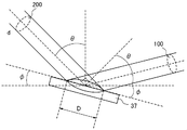
- FIG. 7 is a schematic diagram for explaining a configuration example of a related scanning mirror.
- the scanning angle of the scanning beam light projected on the non-projection surface depends on the tilt angle of the scanning mirror 37.
- ⁇ + ⁇ is within ⁇ 90 degrees, and the scanning angle ⁇ of the scanning mirror 37 is scanned at an equal angle in the ⁇ direction.
- the minimum value of cos ( ⁇ + ⁇ ) is smaller than the minimum value of cos ( ⁇ ). This is because there is an offset of ⁇ ( ⁇ 0).
- the beam light diameter D on the scanning mirror 37 is maximized when cos ( ⁇ + ⁇ ) is minimized, which is when the incident beam light 200 is incident obliquely. .
- the beam light diameter D on the scanning mirror 37 is enlarged compared to the case of perpendicular incidence. Therefore, in order to reflect all of the incident beam light 200, it is necessary to increase the diameter of the scanning mirror 37. Increasing the diameter of the scanning mirror 37 also affects the angle range in which the optical scanning element can scan, thereby limiting the scanning angle. Therefore, increasing the diameter of the scanning mirror 37 leads to a decrease in image quality.
- FIG. 8 is a schematic diagram for explaining the surface reflected beam light 300 generated by the polarization conversion element in the image display device of Patent Document 2.
- FIG. Linearly polarized incident beam light 200 enters the polarization beam splitter 21 from a light source (not shown).
- the polarization direction is, for example, S-polarized light.
- the polarization beam splitter 21 acts so as to reflect the S-polarized light by 90 degrees and not the P-polarized light by 90 degrees
- the incident beam light 200 from the light source 1 is reflected by the polarizing beam splitter 21 by 90 degrees.
- the incident beam light 200 reflected in the direction of the optical scanning element 3 passes through the quarter wavelength plate 61 as a polarization conversion element.
- the surface reflected beam light 300 is generated at the boundary surface where the refractive index difference is generated.
- the surface reflected beam light 300 is generated.
- the surface reflected beam light 300 has the same polarization as the scanning beam light 100 reflected by the optical scanning element 3. This is because the 1 ⁇ 4 wavelength plate 61 is reciprocated. Therefore, the surface reflection beam light 300 that does not pass through the scanning mirror 37 is projected onto the surface to be scanned 4 in the same manner as the scanning beam light 100 that passes through the scanning mirror 37. As a result, the image quality is degraded.
- the surface reflectance R [(n 1 ⁇ n 2 ) / (n 1 + n 2 )] 2 (2) It becomes.
- the formula (2) About 4% of the incident light energy becomes a surface reflection component. Since this surface reflection component is projected as a bright spot on the surface to be scanned, the image quality is significantly lowered.
- the display screen resolution is, for example, SVGA (800 pixels ⁇ 600 pixels).
- an AR (Anti Reflection) coat is applied to the interface between the quarter-wave plate and the air, and the surface reflectance R is 0.5%. This is because, for example, when the AR coating technique using a dielectric multilayer film is used, the surface reflectance can be reduced to about 0.5%.
- Two-dimensional scanning is realized by scanning in the horizontal and vertical directions with a single scanning mirror. Since the beam diameter of the surface reflection beam and the beam diameter on the display screen are substantially equal, the spot on which the bright spot that does not pass through the scanning mirror is projected is 1 / (800 ⁇ 600) of the entire screen.
- the configuration in which the beam light is obliquely incident on the optical scanning element has a problem of image quality deterioration due to the increase in the diameter of the scanning mirror, the influence on the scanning angle, the influence of the occurrence of distortion, and the like. .
- Such a configuration also increases the volume of the optical scanning element.
- the configuration is such that the beam light is vertically incident on the optical scanning element so as to avoid such influence, there is a problem that an adverse effect due to the return light occurs.
- An object of the present invention is to provide an optical scanner and an image display device using the same that solve the above-described problem that the image display device using the optical scanner is large in size and the image quality is lowered. It is to provide.
- an optical scanner of the present invention scans a light source that emits a light beam in a first polarization state, a polarization separation element, and the light beam emitted from the light source toward a surface to be scanned.
- An optical scanning element wherein the optical scanning element converts the incident first polarized light beam into a second polarized light beam and radiates it toward the polarized light separating element.
- the beam light in the polarization state and the beam light in the second polarization state are spatially separated.
- the optical scanner of the present invention and the image display device using the same, it is possible to display a high-quality image without causing an increase in the size of the device.
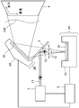
- FIG. 1 is a schematic diagram for explaining a configuration of an image display apparatus having an optical scanner according to the first embodiment of the present invention.
- the image display apparatus according to the present embodiment includes a light source 1, a polarization separation element 2, an optical scanning element 3, and a control unit 5, and displays an image on the scanned surface 4.
- optical components such as a lens, a mirror, and a diffraction grating (not shown) may be provided on the beam light path.
- the light source 1 emits beam light 11 in the first polarization state. More specifically, the light source 1 is configured by, for example, a semiconductor laser element, a solid-state laser element, a beam light shape shaping optical system, or the like that emits light beams having one or more wavelengths. Then, the light source 1 emits the light beam 11 in the first polarization state modulated by the control unit 5 in accordance with the video signal.
- the polarization separation element 2 is provided on the optical path of the beam light emitted from the light source 1. Then, the polarization separation element 2 separates the second polarization state beam light 12 out of the first polarization state light beam 11 and reflects it by 90 degrees in the direction of the optical scanning element 3, and is orthogonal to the second polarization state. And has a function of transmitting light in the third polarization state.
- a plate-type polarization beam splitter or a cube-type polarization beam splitter on which an optical thin film is deposited can be used as the polarization separation element 2.
- the optical scanning element 3 includes a scanning mirror 31 and a scanning mirror driving unit 32, and the scanning mirror 31 is provided on the optical path of the beam light 12 in the second polarization state.
- the scanning mirror 31 has a function of reflecting the incident light beam 12 in the second polarization state in the direction of the polarization separation element 2 and a function of converting the beam light 13 in the third polarization state when reflected. .
- the optical scanning element 3 operates so as to scan the light beam in at least one of the horizontal direction and the vertical direction.
- a resonant MEMS mirror can be used as the optical scanning element 3.
- a polygon mirror, a galvanometer mirror, or the like may be used as the optical scanning element 3.
- the scanned surface 4 includes a scattering surface that transmits and reflects the incident scanning beam and diffuses it.
- the scanned surface 4 may be a fluorescent screen that generates fluorescence by incident beam light.
- FIG. 2 is a schematic diagram for explaining the operation of the optical scanner according to the first embodiment of the present invention.
- the optical scanner of this embodiment includes a light source 1, a polarization separation element 2, and an optical scanning element 3.
- optical components such as a lens, a mirror, a diffraction grating, and a control unit (not shown), a control device, and the like may be provided on the beam light path.
- the light source 1 emits beam light 11 in the first polarization state.
- the light source emits the light beam 11 in the first polarization state modulated by a control unit (not shown) and modulated according to the video signal.
- the polarization separation element 2 separates the second polarization state beam light 12 out of the first polarization state beam light 11 and reflects it 90 degrees in the direction of the optical scanning element 3, and orthogonally crosses the second polarization.
- 3 has a function of transmitting light having a polarization state of 3.
- the optical scanning element 3 includes a scanning mirror 31 and a scanning mirror driving unit 32.
- the scanning mirror 31 has a function of reflecting the incident light beam 12 in the second polarization state in the direction of the polarization separating element 2 and a function of converting the beam light 13 in the third polarization state when reflected. is doing.
- the tilt angle of the scanning mirror 31 is movable. By changing the tilt angle of the scanning mirror 31, the beam light 13 in the third polarization state is deflected and acts as an optical scanner. 1 shows the optical path of the beam light 13 in the third polarization state when the tilt angle (scanning angle) of the scanning mirror 31 is changed, while FIG. 2 shows the tilt angle of the scanning mirror 31 being changed. The optical path when there is no light (when scanning is not performed) is shown. As apparent from FIG. 2, the optical scanning element 3 of the present embodiment is configured such that the beam light enters the optical scanning element 3 substantially vertically.
- a plate-type polarization beam splitter 21 is used as the polarization separation element 2, and the polarization beam splitter 21 is configured to reflect a specific polarization component by 90 degrees.
- the light source 1 emits S-polarized beam light to the polarization beam splitter 21 as the beam light 11 in the first polarization state.
- the polarization beam splitter 21 is configured to reflect S-polarized light by 90 degrees and transmit P-polarized light.
- the polarization beam splitter 21 reflects the light beam 11 (S-polarized light) in the first polarization state toward the optical scanning element 3, and the light beam 11 in the first polarization state is reflected in the second polarization state.
- the light beam 12 is obtained.
- the beam light 12 (S-polarized light) in the second polarization state is incident on the optical scanning element 3 having the scanning mirror 31.
- the scanning mirror 31 operates to reflect the beam light 12 in the second polarization state (S-polarized light) in the direction of the polarization beam splitter 21 and convert it to the beam light 13 in the third polarization state (P-polarized light). To do.
- the scanning mirror driving unit 32 drives the scanning mirror 31 so as to form a scanning pattern of beam light on the scanned surface 4 in accordance with a control signal from the control unit 5.
- the output balance of each wavelength of the light source 1 is modulated according to the deflection angle of the optical scanning element 3 by the control signal of the control unit 5.
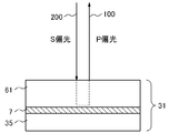
- a scanning mirror 31 having a specific polarization conversion function there is a configuration having a reflecting surface 7 and a transmissive quarter-wave plate 61.
- FIG. 3 is a schematic diagram for explaining the configuration of the scanning mirror 31 used in the implementation state. A transmissive quarter-wave plate 61 and a reflecting surface 7 are formed on the scanning mirror substrate 35.
- the quarter wave plate 61 includes an element made of quartz, birefringent polymer, mica, or the like as a raw material.
- the S-polarized incident beam light 200 that has entered the quarter-wave plate 61 via the polarization beam splitter 21 is converted into circularly-polarized light by the quarter-wave plate 61 when it reaches the reflecting surface 7.
- the reflection surface 7 reflects the light in a circularly polarized state, the phase of the circularly polarized light is reversed.
- the circularly polarized state of the incident beam light 200 travels in a direction opposite to the rotation direction when incident, with respect to the traveling direction of the beam light.
- the reflected circularly polarized light beam propagates again inside the quarter-wave plate 61.
- the S-polarized linearly polarized light incident on the scanning mirror 31 becomes linearly polarized light (P-polarized light) that has been polarization-converted in the polarization direction orthogonal to the S-polarized light.
- the P-polarized beam light is emitted from the scanning mirror 31 as the operation beam light 100.
- the optical scanner according to the present embodiment includes the scanning mirror 31 having the polarization conversion function, and thus the surface reflected beam light having the same polarization direction as the scanning beam light is not used without passing through the optical scanning element 3 in principle. Does not occur. Therefore, a region having a high energy density is not generated locally on the scanned surface 4 due to unnecessary surface reflected beam light, so that a high-quality image can be displayed.
- the light beam is incident on the optical scanning element 3 having the scanning mirror 31 in a substantially vertical direction, the influence of the beam light diameter expansion on the surface of the scanning mirror 31 is minimized. Accordingly, it is possible to avoid an increase in the size of the apparatus due to an increase in the diameter of the scanning mirror 31. Further, the burden on the optical scanning mirror driving unit is reduced, and it is possible to improve performance by expanding the optical scanning range.
- FIG. 4 is a schematic diagram for explaining the configuration of an image display device using an optical scanner according to the second embodiment of the present invention. Individual components included in the present embodiment are the same as those in the first embodiment.
- the light source 1 emits a first polarized light beam 11 modulated by the control unit 5 in accordance with the video signal.
- the polarization separation element 2 is provided on the optical path of the beam light emitted from the light source 1. Then, the polarization separation element 2 separates the light beam 12 in the second polarization state from the light beam 11 in the first polarization state, transmits the light beam 12 in the direction of the optical scanning element 3, and orthogonally crosses the second polarization. 3 has a function of reflecting light in the polarization state 3 by 90 degrees.
- the scanning mirror 31 included in the optical scanning element 3 is provided on the optical path of the beam light 12 in the second polarization state.
- the scanning mirror 31 has a function of reflecting the incident light beam 12 in the second polarization state in the direction of the polarization separation element 2 and a light beam 13 in the third polarization state different from the second polarization state when reflected. And a function to convert. Further, the scanning mirror 31 operates so as to scan the light beam in at least one direction of the horizontal direction and the vertical direction. (Operation)
- the optical path of the light beam and the operation of optical scanning will be described.
- a plate-type polarization beam splitter 21 is used as the polarization separation element 2 and the polarization beam splitter 21 is configured to transmit a specific polarization component.
- the light source 1 emits the first polarization state light beam 11 that is S-polarized light beam toward the polarization beam splitter 21.
- the polarization beam splitter 21 is configured to transmit S-polarized light and reflect P-polarized light by 90 degrees. At this time, the polarization beam splitter 21 transmits the light beam 11 (S-polarized light) in the first polarization state toward the optical scanning element 3 as the light beam 12 in the second polarization state.
- the second polarized light beam (S-polarized light) is incident on the optical scanning element 3 having the scanning mirror 31 having a polarization conversion function.
- the scanning mirror 31 operates to reflect the beam light 12 in the second polarization state (S-polarized light) in the direction of the polarization beam splitter 21 and convert it to the beam light 13 in the third polarization state (P-polarized light). To do.
- the scanning mirror driving unit 32 deflects the scanning mirror 31 so as to form a scanning pattern on the scanned surface 4 in accordance with a control signal from the control unit 5.
- the image display apparatus according to the present embodiment is configured such that the light beam 11 in the first polarization state travels straight from the light source 1 toward the optical scanning element 3 via the polarization separation element 2. Therefore, in addition to the same effects as those of the first embodiment, the following new effects are achieved. That is, since the light path travels straight, the optical axis can be easily adjusted.
- FIG. 5 is a schematic diagram for explaining a configuration of an image display apparatus having an optical scanner according to the third embodiment of the present invention.
- This embodiment has a configuration having two optical scanning elements.
- the two optical scanning elements 3A and 3B have scanning mirrors 31 and 33 and scanning mirror driving units 32 and 34, respectively.
- the scanning mirror driving units 32 and 34 deflect the scanning beam 100 in the horizontal direction or the vertical direction based on the control signal of the control unit 5, respectively.
- the light source 1 emits a first polarized light beam 11 modulated by the control unit 5 in accordance with the video signal.
- the polarization separation element 2 When the light beam 11 in the first polarization state is incident, the polarization separation element 2 reflects the light beam in the second polarization state by 90 degrees, and in the third polarization state orthogonal to the second polarization state. It has a function of transmitting light.
- the light beam 11 in the first polarization state incident on the polarization separation element 2 is reflected 90 degrees in the direction of the scanning mirror 31 included in the first optical scanning element 3A, and becomes the light beam 12 in the second polarization state.
- the scanning mirror 31 has a function of reflecting the incident light beam 12 in the second polarization state in the direction of the polarization separation element 2 and a function of converting the light beam 13 in the third polarization state.
- the scanning mirror 31 operates so as to scan the beam light in at least one direction of the horizontal direction and the vertical direction.
- the second optical scanning element 3B After exiting from the optical scanning element 3A, the second optical scanning element 3B is provided on the optical path of the beam light 13 in the third polarization state that has passed through the polarization separation element 2.
- the scanning mirror 33 has a function of reflecting incident beam light in the direction of the scanned surface 4. Then, the second optical scanning element 3B operates to scan the beam light 13 in the third polarization state in a direction different from the scanning direction of the first optical scanning element 3A.
- the scanning mirror 33 used in this embodiment does not need to have a function of converting polarized light. (Operation)
- the optical path of the light beam and the operation of optical scanning will be described.
- a plate-type polarization beam splitter 21 is used as the polarization separation element 2, and the polarization beam splitter 21 is configured to reflect a specific polarization component by 90 degrees.
- the optical scanning element 3A scans in the vertical direction with respect to the scanned surface 4, and the optical scanning element 3B scans in the horizontal direction with respect to the scanned surface 4.
- the light source 1 emits the first polarization state light beam 11 that is S-polarized light beam toward the polarization beam splitter 21.
- the polarization beam splitter 21 is configured to reflect S-polarized light by 90 degrees and transmit P-polarized light.
- the polarization beam splitter 21 reflects the light beam 11 (S-polarized light) in the first polarization state 90 degrees toward the optical scanning element 3A as the beam light 12 (S-polarized light) in the second polarization state. Then, the light beam (S-polarized light) in the second polarization state enters the optical scanning element 3A including the scanning mirror 31 having a polarization conversion function.
- the scanning mirror 31 operates so as to reflect the second polarized light beam 12 (S-polarized light) in the direction of the polarizing beam splitter and convert it into the third polarized light beam 13 (P-polarized light).
- the scanning mirror drive unit 32 deflects the scanning mirror 31 according to the control signal from the control unit 5 so that the beam light is scanned in the vertical direction on the scanned surface 4.
- the image display apparatus is configured to have two optical scanning elements 3A and 3B for scanning in two directions, horizontal and vertical.
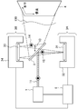
- FIG. 6 is a schematic diagram for explaining the configuration of an image display apparatus using an optical scanner according to the fourth embodiment of the present invention.
- This embodiment also has a configuration including two optical scanning elements.
- the difference between the third embodiment and the present embodiment is that each of the two scanning mirrors 3A and 3B has a polarization conversion function.
- the light source 1 emits a first polarized light beam 11 modulated by the control unit 5 in accordance with the video signal.
- the polarization separation element 2 reflects the light beam in the second polarization state by 90 degrees, and in the third polarization state orthogonal to the second polarization state. It has a function of transmitting light.
- the light beam 11 in the first polarization state incident on the polarization separation element 2 is reflected by 90 degrees toward the scanning mirror 31 included in the first optical scanning element 3A, and becomes the light beam 12 in the second polarization state. .
- the scanning mirror 31 has a function of reflecting the incident light beam 12 in the second polarization state in the direction of the polarization separation element 2 and a function of converting the light beam 13 in the third polarization state.
- the scanning mirror 31 operates so as to scan the light beam in one of the horizontal direction and the vertical direction.
- the second optical scanning element 3B is on the optical path of the beam light that has passed through the polarization separation element 2 out of the third polarized light beam 13 emitted from the optical scanning element 3A.
- the scanning mirror 33 has a function of reflecting incident beam light in the direction of the surface to be scanned 4 and a function of converting the beam light 14 into a fourth polarization state. Then, the second optical scanning element 3B operates to scan the beam light 13 in the third polarization state in a direction different from the scanning direction of the first optical scanning element 3A. (Operation)
- the optical path of the light beam and the operation of optical scanning will be described.
- a plate-type polarization beam splitter 21 is used as the polarization separation element 2, and the polarization beam splitter 21 is configured to reflect a specific polarization component by 90 degrees.
- the optical scanning element 3A scans in the vertical direction
- the optical scanning element 3B scans in the horizontal direction.
- the light source 1 emits the first polarization state light beam 11 that is S-polarized light beam toward the polarization beam splitter 21.
- the polarization beam splitter 21 is configured to reflect S-polarized light by 90 degrees and transmit P-polarized light.
- the polarization beam splitter 21 reflects the light beam 11 (S-polarized light) in the first polarization state by 90 degrees toward the optical scanning element 3A to obtain the light beam 12 in the second polarization state. Then, the light beam 12 (S-polarized light) in the second polarization state enters the optical scanning element 3A having the scanning mirror 31 having a polarization conversion function.
- the scanning mirror 31 operates so as to reflect the second polarized light beam 12 (S-polarized light) in the direction of the polarizing beam splitter and convert it into the third polarized light beam 13 (P-polarized light).
- the scanning mirror driving unit 32 drives the scanning mirror 31 according to the control signal from the control unit 5 so that the beam light is scanned in the vertical direction on the surface to be scanned 4.
- the beam light transmitted through the polarization beam splitter 21 enters the optical scanning element 3B.
- the scanning mirror 33 operates to reflect the beam light transmitted through the polarization beam splitter 21 in the direction of the surface to be scanned 4 and to convert the beam light 14 (S-polarized light) in the fourth polarization state.
- the light beam 14 (S-polarized light) in the fourth polarization state is reflected by the polarization separation element 2 by 90 degrees, reaches the scanned surface 4, and becomes the scanning beam light 100.
- the scanning mirror driving unit 34 drives the scanning mirror 33 so that the beam light is scanned in the horizontal direction on the surface to be scanned 4 according to the control signal of the control unit 5.
- the scanning beam light 100 two-dimensionally scanned on the non-scanning surface is projected.
- the image display apparatus according to the present embodiment includes two optical scanning elements, both of which are configured such that beam light is incident substantially vertically. Therefore, in addition to the same effects as those of the third embodiment, the following new effects are achieved. That is, since the incident light beam to the optical scanning element 3B having the scanning mirror 33 is not oblique, the influence of the beam light diameter expansion on the surface of the scanning mirror 33 is minimized. Accordingly, an increase in aperture of the scanning mirror 33 can be suppressed. As a result, it is possible to reduce the size of the apparatus, reduce the burden on the optical scanning mirror driving unit, and improve the performance by expanding the optical scanning range.
- the polarization state of the beam light emitted from the light source may be linearly polarized light, circularly polarized light, or elliptically polarized light.
- the polarization beam splitter may be provided with a polarization / transmission characteristic different from the description example of the embodiment with respect to the separation characteristic between the S-polarized light and the P-polarized light.
- the light beams other than in the second polarization state may be incident on a beam stopper provided at a position that does not spatially interfere with the scanning beam.
- the reflection direction of the scanning beam by the scanning mirror may be perpendicular to the light source side or the paper surface in each drawing as long as it does not interfere with the scanning beam region.
- the scanning order may be either the horizontal direction or the vertical direction first.
- a light source that emits beam light in a first polarization state
- a polarization separation element An optical scanning element that scans the beam light emitted from the light source toward the surface to be scanned, The optical scanning element converts the incident beam light in the first polarization state into a beam light in the second polarization state, and radiates it toward the polarization separation element
- the polarization separation element is an optical scanner that spatially separates the light beam in the first polarization state and the light beam in the second polarization state.
- (Appendix 2) The optical scanner according to appendix 1, wherein the optical scanning element reflects incident beam light and gives a phase difference corresponding to a half wavelength between two orthogonal polarization components of the incident beam light.
- the optical scanning element includes a phase shifter that gives a phase difference of 1 ⁇ 4 wavelength between two orthogonal polarization components of the incident beam light; A reflection surface formed integrally with the phase shifter; The optical scanner according to claim 1, wherein the incident beam light is emitted after reciprocating in the phase shifter by the reflecting surface.
- (Appendix 4) The optical scanner according to appendix 3, wherein the phase shifter is a quarter-wave plate.
- the said polarization separation element is characterized by deflecting one polarization with respect to the light beam of the said 1st polarization state, and the beam light of the said 2nd polarization state, and not deflecting other polarization
- the optical scanner according to appendix 1. The optical scanning element includes: a first optical scanning element that scans incident beam light in a first direction; A second optical scanning element that scans the incident light beam in a second direction different from the first direction; The optical scanner according to any one of appendices 1 to 5, including: (Appendix 7) The optical scanner according to appendix 6, wherein the second optical scanning element reflects incident beam light in the direction of the surface to be scanned.
- the present invention is applicable to, for example, an optical scanner used for image display and an image display device using the same.
Landscapes
- Physics & Mathematics (AREA)
- General Physics & Mathematics (AREA)
- Optics & Photonics (AREA)
- Mechanical Optical Scanning Systems (AREA)
Description
本発明は、光走査器およびそれを用いた画像表示装置に関し、特に、ビーム光を被走査面上に走査して画像を表示する光走査器およびそれを用いた画像表示装置に関する。
赤色、緑色、青色のビーム光を2次元走査して画像を表示する、走査型レーザプロジェクタが多く提案されている。
例えば、特許文献1には、画像信号で変調された赤色、緑色、青色のビーム光を合成し、光走査素子によって被投射面に画像を表示する投射型表示装置が記載されている。より詳細には、光源からそれぞれ発する赤色、緑色、青色のビーム光は色合成素子で合成される。そして、合成されたビーム光は、水平方向および垂直方向に光走査を行う2つの光走査素子によって、2次元的に走査されている。その結果、色合成され2次元的に走査されたビーム光が、被投射面上にカラー画像として表示される。この構成において、ビーム光を被投射面に向けて走査し、かつ、走査中にビーム光を画素間で区切ることでパルス光として放射することが特徴であるとしている。その結果、画像むらのない高精細な投射画像が得ることができるとしている。
また、特許文献2には、変調されたビーム光を出射する1つ以上の光源、ビーム整形光学素子、ビーム結合器、選択性折り畳みミラー、偏光変換素子、そしてビーム光を偏向する光走査素子である走査ミラーを備えた統合型フォトニックモジュールの構成が記載されている。光源から出力される変調ビーム光は直線偏光であり、電界成分が垂直方向であるS偏光となっている。変調ビーム光は、ビーム整形光学素子を介してビーム結合器へ向かう。ビーム結合器は、変調されたビーム光のS偏光成分を結合させる。選択制折り畳みミラーは、例えば偏光ビームスプリッタであり、S偏光成分を90度反射させ、P偏光成分を90度反射させずそのまま透過させる。そのため、S偏光である変調合成ビーム光は、選択性折り畳みミラーにおいて、走査ミラー側に偏向して進む。走査ミラーに向かう経路上には偏光変換素子が配置されている。偏光変換素子は、例えば1/4波長板であり、S偏光は円偏光に変換される。そして、走査ミラー入射した円偏光は、走査ミラーで反射され、偏光変換素子を再度透過した際にはP偏光になる。走査ミラーからの出射光であるP偏光の走査ビーム光は、偏光ビームスプリッタにおいては偏向せずにそのまま透過し、その結果、走査ビーム光は被走査面に投射される。このように、コンパクトな走査型レーザプロジェクタが実現できるとしている。なお、特許文献1および特許文献2には、前述とは別の実施形態として、走査ミラーを有する光走査素子に対して、変調合成ビーム光を斜めに入射する構成も記載されている。
しかしながら、これら文献に記載の光走査器およびそれを用いた画像表示装置には次のような問題があった。
特許文献1および特許文献2の別の実施形態においては、走査ミラーを有する光走査素子に対してビーム光が斜めに入射する構成である。そのため、走査ミラー上での見かけのビーム径がより拡大される。その結果、走査ミラーが大口径化し、ひいては装置の体積が増大する、という問題があった。
他方、特許文献2の実施形態では、走査ミラーを有する光走査素子に対してビーム光が垂直に入射する構成としている。この場合、走査ミラー上での見かけのビーム径の拡大は最小に抑えられるものの、表面反射による戻り光によって画質が劣化するという問題があった。
上記問題に対して、出願人は以下のような詳細分析を行った。
まず、走査ミラー上での見かけのビーム径がより拡大する問題について検討する。
一般に、走査型レーザプロジェクタの解像度は、走査ミラーの走査角度と走査ミラー径との積によって規定される。その理由は、走査型レーザプロジェクタの解像度は、走査ビームが被走査面上に形成するビームスポットの配列量で決定されるからである。そうすると、解像度の高い画像(高画質な画像)を表示するためには、被走査面上で小さなビームスポットを形成し、かつ、光走査素子の走査角度が大きいことが必要となる。その一方で、被走査面上でのビームスポットの縮小化と、走査角度の拡大化とは二律背反の関係にある。従って、解像度の高い画像(高画質な画像)を実現することは困難である。
図7は、関連する走査ミラーの構成例を説明するための模式図である。走査ミラー37を傾けることで、走査ミラーで反射したビーム光の戻り方向を変えている。即ち、非投射面に投射される走査ビーム光の走査角度は、走査ミラー37の傾け角度に依存する。図7に示すように、入射ビームが斜めに走査ミラー37に入射する場合を考える。走査ミラー37上でのビーム光径Dは、入射ビーム光200のビーム径および走査ビーム光100のビーム径をd、走査をしていない状態でのビーム光の走査ミラー37への入射角をθ、走査ミラー37の機械的な走査角度をφとすると、
D=d/cos(φ+θ) ・・・(1)
と表すことができる。φ+θは±90度以内であり、走査ミラー37の走査角度φは±方向に均等な角度で各々走査されるものとする。ここで、入射ビーム光200が斜入射する場合(θ≠0)と、入射ビーム光200が垂直入射する場合(θ=0)とを比較する。φを±方向に均等に変化させる場合、cos(φ+θ)の最小値は、cos(φ)の最小値よりも小さくなる。これは、θ(≠0)分のオフセットがあるからである。そうすると、式(1)より、走査ミラー37上でのビーム光径Dが最大値となるのは、cos(φ+θ)が最小となる場合であり、それは入射ビーム光200が斜入射する場合である。以上のように、斜め入射の場合には、垂直入射する場合よりも、走査ミラー37上でのビーム光径Dが拡大される。そのため、入射ビーム光200の全てを反射させるためには走査ミラー37を大口径化することが必要になる。走査ミラー37の大口径化は、光走査素子が走査できる角度範囲にも影響を与え、走査角度が制限されることとなる。従って、走査ミラー37の大口径化は、画質の低下につながる。
D=d/cos(φ+θ) ・・・(1)
と表すことができる。φ+θは±90度以内であり、走査ミラー37の走査角度φは±方向に均等な角度で各々走査されるものとする。ここで、入射ビーム光200が斜入射する場合(θ≠0)と、入射ビーム光200が垂直入射する場合(θ=0)とを比較する。φを±方向に均等に変化させる場合、cos(φ+θ)の最小値は、cos(φ)の最小値よりも小さくなる。これは、θ(≠0)分のオフセットがあるからである。そうすると、式(1)より、走査ミラー37上でのビーム光径Dが最大値となるのは、cos(φ+θ)が最小となる場合であり、それは入射ビーム光200が斜入射する場合である。以上のように、斜め入射の場合には、垂直入射する場合よりも、走査ミラー37上でのビーム光径Dが拡大される。そのため、入射ビーム光200の全てを反射させるためには走査ミラー37を大口径化することが必要になる。走査ミラー37の大口径化は、光走査素子が走査できる角度範囲にも影響を与え、走査角度が制限されることとなる。従って、走査ミラー37の大口径化は、画質の低下につながる。
また、斜め入射においては歪曲収差が発生し、それを補正する構造や調整機能が必要となり装置が複雑化・大型化する、といった問題も生じる。
次に、表面反射による戻り光により画質が劣化する問題について検討する。
図8は、特許文献2の画像表示装置において、偏光変換素子で発生する表面反射ビーム光300について説明するための概略図である。図示していない光源から直線偏光の入射ビーム光200が、偏光ビームスプリッタ21に入射する。偏光方向は例えばS偏光である。ここで、偏光ビームスプリッタ21が、S偏光を90度反射し、P偏光を90度反射しないように作用する場合、光源1からの入射ビーム光200は偏光ビームスプリッタ21において90度反射される。光走査素子3の方向に反射した入射ビーム光200が、偏光変換素子としての1/4波長板61を透過する。その際、入射ビーム光の光路に屈折率差が存在すると、その屈折率差が生じている境界面において表面反射ビーム光300が発生する。ここで、1/4波長板61と空気層との間に屈折率差が存在するため、表面反射ビーム光300が発生する。この表面反射ビーム光300は、光走査素子3で反射した走査ビーム光100と同じ偏光となる。それは、1/4波長板61を往復することになるからである。そのため、走査ミラー37を経由しない表面反射ビーム光300が、走査ミラー37を経由した走査ビーム光100と同じく、被走査面4に投射されることになる。その結果、画質が低下することになる。
一般的に、光が屈折率n1から屈折率n2の物質に垂直入射するとき、表面反射率Rは、
R=[(n1-n2)/(n1+n2)]2 ・・・(2)
となる。具体的な数値例として、1/4波長板(屈折率:1.5)、1/4波長板と走査ミラーの間の空間は空気(屈折率:1.0)とすると、式(2)より入射した光エネルギーのうち約4%が表面反射成分となる。この表面反射成分が、被走査面では輝点として投射されるために画質が著しく低下することになる。
R=[(n1-n2)/(n1+n2)]2 ・・・(2)
となる。具体的な数値例として、1/4波長板(屈折率:1.5)、1/4波長板と走査ミラーの間の空間は空気(屈折率:1.0)とすると、式(2)より入射した光エネルギーのうち約4%が表面反射成分となる。この表面反射成分が、被走査面では輝点として投射されるために画質が著しく低下することになる。
画質低下の程度について、以下では定量的に検討する。そのため、ビーム光の表面反射によって表示画面上に発生する輝点と、輝点を含まない表示画面全体のエネルギー密度とを比較する。前提として、表示画面の解像度を例えばSVGA(800画素×600画素)とする。また、1/4波長板と空気の界面にはAR(Anti Refrection)コートが施されており、表面反射率Rは0.5%とする。その理由は、例えば、誘電体多層膜によるARコートの技術を用いた場合、表面反射率は0.5%程度まで低減可能だからである。また、2次元走査は、1つの走査ミラーで水平および垂直方向に走査して実現するものとする。表面反射ビームのビーム径と表示画面上のビーム径とはほぼ等しいため、走査ミラーを経由しない輝点が投射されるスポットは、画面全体の1/(800×600)となる。
以上を勘案すると、輝点のエネルギー密度は、表示画面全体のエネルギー密度の2412倍(=0.5%/(99.5%/800×600))となる。そうすると、この輝点は観察者に認識されうるレベルとなる。このようにARコートを施したとしても画質低下の影響は避けられない。
以上述べてきたように、光走査素子にビーム光が斜めに入射するような構成は、走査ミラーの大口径化および走査角度への影響、歪曲収差発生の影響、等による画質低下が問題となる。また、このような構成は光走査素子の体積増加をもたらす。その一方で、このような影響を避けるべく光走査素子にビーム光が垂直に入射するような構成にすると、戻り光による悪影響が発生するという問題がある。
本発明の目的は、上述した課題である、光走査器を用いた画像表示装置では、装置が大型化し、画質が低下する、という課題を解決する光走査器およびそれを用いた画像表示装置を提供することにある。
上記目的を達成するため、本発明の光走査器は、第1の偏光状態のビーム光を出射する光源と、偏光分離素子と、光源から出射されたビーム光を被走査面に向けて走査させる光走査素子とを含み、光走査素子は入射した第1の偏光状態のビーム光を第2の偏光状態のビーム光に変換して偏光分離素子に向けて放射し、偏光分離素子は第1の偏光状態のビーム光と第2の偏光状態のビーム光とに空間的に分離する。
本発明の光走査器およびそれを用いた画像表示装置によれば、装置の大型化を招くことなく高画質な画像を表示することができる。
次に、本発明を実施するための形態について図面を参照して説明する。なお、以下の説明では、同じ機能を有するものには同じ符号をつけ、その説明を省略する場合がある。
(第1の実施形態)
(画像表示装置の構成)
図1は、本発明の第1の実施形態である光走査器を有する画像表示装置の構成を説明するための概略図である。図1に示すように、本実施形態の画像表示装置は、光源1と、偏光分離素子2と、光走査素子3と、制御部5とを有し、被走査面4上に画像を表示する。なお、本実施形態では、ビーム光の経路上に図示しないレンズ、ミラー、回折格子などの光学部品を備えてもよい。
(第1の実施形態)
(画像表示装置の構成)
図1は、本発明の第1の実施形態である光走査器を有する画像表示装置の構成を説明するための概略図である。図1に示すように、本実施形態の画像表示装置は、光源1と、偏光分離素子2と、光走査素子3と、制御部5とを有し、被走査面4上に画像を表示する。なお、本実施形態では、ビーム光の経路上に図示しないレンズ、ミラー、回折格子などの光学部品を備えてもよい。
光源1は、第1の偏光状態のビーム光11を出射する。より具体的には、光源1は、例えば、1つ以上の波長のビーム光を出射する半導体レーザ素子や固体レーザ素子、ビーム光形状整形光学系などで構成される。そして、光源1は映像信号に応じて制御部5によって変調された第1の偏光状態のビーム光11を出射する。
偏光分離素子2は、光源1から出射したビーム光の光路上に設けられる。そして、偏光分離素子2は、第1の偏光状態のビーム光11のうち、第2の偏光状態のビーム光12を分離して光走査素子3方向に90度反射させ、第2の偏光と直交する第3の偏光状態の光を透過させる機能を有する。偏光分離素子2として例えば、光学薄膜を蒸着したプレート型偏光ビームスプリッタや、キューブ型偏光ビームスプリッタを用いることができる。
光走査素子3は、走査ミラー31と走査ミラー駆動部32を有し、走査ミラー31は第2の偏光状態のビーム光12の光路上に設けられる。走査ミラー31は、入射した第2の偏光状態のビーム光12を偏光分離素子2の方向に反射させる機能と、反射させたときに第3の偏光状態のビーム光13に変換する機能とを有する。そして、光走査素子3はビーム光を水平方向および垂直方向の少なくとも一方向に走査するように動作する。光走査素子3としては例えば、共振型のMEMSミラーを用いることができる。これに限らず、光走査素子3としてポリゴンミラー、ガルバノミラーなどを用いてもよい。
なお、被走査面4としては、入射した走査ビームを透過および反射し拡散する散乱面がある。その他には、被走査面4は、入射したビーム光によって蛍光を発生させる蛍光スクリーンであってもよい。
(光走査器の構成)
図2は、本発明の第1の実施形態である光走査器の動作を説明するための模式図である。本実施形態の光走査器は、光源1と、偏光分離素子2と、光走査素子3と、を有する。なお、本実施形態では、ビーム光の経路上に図示しないレンズ、ミラー、回折格子、制御部などの光学部品や制御装置などを備えてもよい。
(光走査器の構成)
図2は、本発明の第1の実施形態である光走査器の動作を説明するための模式図である。本実施形態の光走査器は、光源1と、偏光分離素子2と、光走査素子3と、を有する。なお、本実施形態では、ビーム光の経路上に図示しないレンズ、ミラー、回折格子、制御部などの光学部品や制御装置などを備えてもよい。
光源1は、第1の偏光状態のビーム光11を出射する。光源は、例えば、図示しない制御部によって変調され、映像信号に応じて変調された第1の偏光状態のビーム光11を出射する。
偏光分離素子2は、第1の偏光状態のビーム光11のうち、第2の偏光状態のビーム光12を分離して光走査素子3方向に90度反射させ、第2の偏光と直交する第3の偏光状態の光を透過させる機能を有する。
光走査素子3は、走査ミラー31と走査ミラー駆動部32を有する。走査ミラー31は、入射した第2の偏光状態のビーム光12を偏光分離素子2の方向に反射させる機能と、反射させたときに第3の偏光状態のビーム光13に変換する機能とを有している。
走査ミラー31の傾斜角は可動である。走査ミラー31の傾斜角度が変化することによって、第3の偏光状態のビーム光13は偏向されて光走査器として作用する。なお、図1は走査ミラー31の傾斜角度(走査角)を変化させた場合における第3の偏光状態のビーム光13の光路を示し、一方、図2は走査ミラー31の傾斜角を変化させていない場合(走査をしていない状態)での光路を示す。図2より明らかなように、本実施形態の光走査素子3は、光走査素子3にビーム光が略垂直に入射する構成である。
(動作)
以下では、ビーム光の光路および光走査の動作について詳細に説明する。
以下では、ビーム光の光路および光走査の動作について詳細に説明する。
偏光分離素子2としてプレート型偏光ビームスプリッタ21を用い、偏光ビームスプリッタ21は特定の偏光成分を90度反射するように構成されているとする。
光源1は、第1の偏光状態のビーム光11として、偏光ビームスプリッタ21に対してS偏光のビーム光を出射する。偏光ビームスプリッタ21は、S偏光を90度反射し、P偏光を透過するように構成されているとする。
このとき、偏光ビームスプリッタ21は、第1の偏光状態のビーム光11(S偏光)を、光走査素子3に向かって反射させ、第1の偏光状態のビーム光11は第2の偏光状態のビーム光12となる。第2の偏光状態のビーム光12(S偏光)は、走査ミラー31を有する光走査素子3に入射する。
走査ミラー31は、第2の偏光状態のビーム光12(S偏光)を、偏光ビームスプリッタ21の方向に反射するとともに、第3の偏光状態のビーム光13(P偏光)に変換するように動作する。走査ミラー駆動部32は、制御部5の制御信号に従って被走査面4上にビーム光の走査パターンを形成するように、走査ミラー31を駆動する。制御部5の制御信号により、光走査素子3の偏向角度に応じて光源1の各波長の出力バランスが変調される。
光走査素子3から出射した第3の偏光状態のビーム光13(P偏光)は、再度偏光ビームスプリッタ21に入射する。偏光ビームスプリッタ21は、P偏光を透過するように構成されているため、第3の偏光状態のビーム光13(P偏光)は走査ビーム100として被走査面4に投射される。
(走査ミラーの具体的構成)
具体的な偏光変換機能を有する走査ミラー31として、反射面7と透過型1/4波長板61を有する構成がある。図3は、実施状態で用いる走査ミラー31の構成を説明するための模式図である。透過型1/4波長板61と反射面7とが走査ミラー基板35上に形成されている。1/4波長板61としては、水晶、複屈折ポリマー、雲母などを原材料とした素子がある。図3を用いて、ビーム光が、反射面7と透過型1/4波長板61が積層された走査ミラー31に、入射および反射するときの偏光状態の変化について説明する。偏光ビームスプリッタ21を介して1/4波長板61に入射したS偏光の入射ビーム光200は、反射面7に到達時には1/4波長板61によって円偏光に変換される。そして、反射面7において円偏光状態で反射する際、円偏光の位相が反転する。そのため、入射ビーム光200は、反射面7で反射後、その円偏光状態がビーム光の進行方向に対して、入射したときの回転方向とは反対方向に回転して進行するようになる。反射した円偏光のビーム光は、1/4波長板61の内部を再び伝搬する。その結果、1/4波長板を2回透過するため1/2波長板を透過したことと等価となる。従って、走査ミラー31に入射したS偏光の直線偏光は、S偏光と直交する偏光方向に偏光変換された直線偏光(P偏光)となる。そして、P偏光となったビーム光は、操作ビーム光100として走査ミラー31から出射する。
(効果)
このように、本実施形態の光走査器では、偏光変換機能を有する走査ミラー31を備えているため、光走査素子3を経由せずに走査ビーム光と同じ偏光方向の表面反射ビーム光が原理的に発生しない。従って、不要な表面反射ビーム光によって被走査面4においてエネルギー密度が局所的に大きい領域が発生することはないため、高画質な画像を表示することが可能となる。
(走査ミラーの具体的構成)
具体的な偏光変換機能を有する走査ミラー31として、反射面7と透過型1/4波長板61を有する構成がある。図3は、実施状態で用いる走査ミラー31の構成を説明するための模式図である。透過型1/4波長板61と反射面7とが走査ミラー基板35上に形成されている。1/4波長板61としては、水晶、複屈折ポリマー、雲母などを原材料とした素子がある。図3を用いて、ビーム光が、反射面7と透過型1/4波長板61が積層された走査ミラー31に、入射および反射するときの偏光状態の変化について説明する。偏光ビームスプリッタ21を介して1/4波長板61に入射したS偏光の入射ビーム光200は、反射面7に到達時には1/4波長板61によって円偏光に変換される。そして、反射面7において円偏光状態で反射する際、円偏光の位相が反転する。そのため、入射ビーム光200は、反射面7で反射後、その円偏光状態がビーム光の進行方向に対して、入射したときの回転方向とは反対方向に回転して進行するようになる。反射した円偏光のビーム光は、1/4波長板61の内部を再び伝搬する。その結果、1/4波長板を2回透過するため1/2波長板を透過したことと等価となる。従って、走査ミラー31に入射したS偏光の直線偏光は、S偏光と直交する偏光方向に偏光変換された直線偏光(P偏光)となる。そして、P偏光となったビーム光は、操作ビーム光100として走査ミラー31から出射する。
(効果)
このように、本実施形態の光走査器では、偏光変換機能を有する走査ミラー31を備えているため、光走査素子3を経由せずに走査ビーム光と同じ偏光方向の表面反射ビーム光が原理的に発生しない。従って、不要な表面反射ビーム光によって被走査面4においてエネルギー密度が局所的に大きい領域が発生することはないため、高画質な画像を表示することが可能となる。
さらに、走査ミラー31を有する光走査素子3へビーム光が略垂直方向で入射する構成であるため、走査ミラー31面上でのビーム光径拡大の影響が最小となる。従って、走査ミラー31の口径増加による装置の大型化を回避することができる。さらに、光走査ミラー駆動部の負担が減少し、光走査範囲の拡大による性能向上を図ることが可能となる。
なお、光走査素子によって偏向された走査ビームは空間的に拡がって1/4波長板に入射する。そのため、1/4波長板は走査ビーム全てが通過しうる表面積を確保する必要がある。この点において、本実施形態では、1/4波長板を走査ミラーに配置した構成としているので走査ビームの拡がりを最小にでき、装置の小型化を図ることができる。
(第2の実施形態)
図4は、本発明の第2の実施形態である光走査器を用いた画像表示装置の構成を説明するための概略図である。本実施形態が有する個々の構成要素は第1の実施形態と同様である。
(構成)
光源1は、映像信号に応じて制御部5によって変調された第1の偏光状態のビーム光11を出射する。
(第2の実施形態)
図4は、本発明の第2の実施形態である光走査器を用いた画像表示装置の構成を説明するための概略図である。本実施形態が有する個々の構成要素は第1の実施形態と同様である。
(構成)
光源1は、映像信号に応じて制御部5によって変調された第1の偏光状態のビーム光11を出射する。
偏光分離素子2は、光源1から出射したビーム光の光路上に設けられる。そして、偏光分離素子2は、第1の偏光状態のビーム光11のうち、第2の偏光状態のビーム光12を分離して光走査素子3方向に透過させ、第2の偏光と直交する第3の偏光状態の光を90度反射させる機能を有する。
光走査素子3に含まれる走査ミラー31は、第2の偏光状態のビーム光12の光路上に設けられる。走査ミラー31は、入射した第2の偏光状態のビーム光12を偏光分離素子2の方向に反射させる機能と、反射するときに第2の偏光状態と異なる第3の偏光状態のビーム光13に変換する機能とを有する。さらに、走査ミラー31はビーム光を水平方向および垂直方向の少なくとも一方向に走査するように動作する。
(動作)
以下では、ビーム光の光路および光走査の動作について説明する。
(動作)
以下では、ビーム光の光路および光走査の動作について説明する。
偏光分離素子2としてプレート型偏光ビームスプリッタ21を用い、偏光ビームスプリッタ21は特定の偏光成分を透過するように構成されているとする。
光源1は、S偏光のビーム光である第1の偏光状態のビーム光11を偏光ビームスプリッタ21に向けて出射する。偏光ビームスプリッタ21は、S偏光を透過させ、P偏光を90度反射するように構成されている。このとき、偏光ビームスプリッタ21は、第1の偏光状態のビーム光11(S偏光)を、第2の偏光状態のビーム光12として光走査素子3に向け透過させる。第2の偏光状態のビーム光(S偏光)は、偏光変換機能を有する走査ミラー31を有する光走査素子3に入射する。
走査ミラー31は、第2の偏光状態のビーム光12(S偏光)を、偏光ビームスプリッタ21の方向に反射するとともに、第3の偏光状態のビーム光13(P偏光)に変換するように動作する。走査ミラー駆動部32は、制御部5の制御信号に従って、被走査面4に走査パターンを形成するように走査ミラー31を偏向する。
光走査素子3から出射した第3の偏光状態のビーム光13(P偏光)は再度偏光ビームスプリッタ21に入射する。偏光ビームスプリッタ21はP偏光を90度反射するように構成されているため、第3の偏光状態のビーム光13(P偏光)は走査ビーム100として被走査面4に投射される。
(効果)
本実施形態に係る画像表示装置は、第1の偏光状態のビーム光11が、偏光分離素子2を介して、光源1から光走査素子3に向けて直進する構成である。そのため、第1の実施形態と同等の効果に加え、以下のような新たな効果を奏する。即ち、直進する光路であるため、光軸調整が容易になる。また、光源1と被走査面4に対する光走査素子3の配置が略90度相違する構成であるため、画像表示装置の設計の自由度が高まる。
(第3の実施形態)
図5は、本発明の第3の実施形態である光走査器を有する画像表示装置の構成を説明するための概略図である。本実施形態は、光走査素子を2つ有する構成である。2つの光走査素子3A、3Bは、走査ミラー31、33および走査ミラー駆動部32、34をそれぞれ有する。走査ミラー駆動部32、34は、制御部5の制御信号に基づいて走査ビーム100を水平方向または垂直方向に、それぞれ偏向する。
(構成)
光源1は、映像信号に応じて制御部5によって変調された第1の偏光状態のビーム光11を出射する。偏光分離素子2は、第1の偏光状態であるビーム光11が入射したとき、第2の偏光状態のビーム光を90度反射させ、また、第2の偏光と直交する第3の偏光状態の光を透過させる機能を有する。偏光分離素子2に入射した第1の偏光状態のビーム光11は、第1の光走査素子3Aに含まれる走査ミラー31方向に90度反射され、第2の偏光状態のビーム光12となる。走査ミラー31は、入射した第2の偏光状態のビーム光12について、偏光分離素子2の方向に反射する機能と、第3の偏光状態のビーム光13に変換する機能とを有する。そして、走査ミラー31は、ビーム光を水平方向および垂直方向の少なくとも一方向に走査するように動作する。
(効果)
本実施形態に係る画像表示装置は、第1の偏光状態のビーム光11が、偏光分離素子2を介して、光源1から光走査素子3に向けて直進する構成である。そのため、第1の実施形態と同等の効果に加え、以下のような新たな効果を奏する。即ち、直進する光路であるため、光軸調整が容易になる。また、光源1と被走査面4に対する光走査素子3の配置が略90度相違する構成であるため、画像表示装置の設計の自由度が高まる。
(第3の実施形態)
図5は、本発明の第3の実施形態である光走査器を有する画像表示装置の構成を説明するための概略図である。本実施形態は、光走査素子を2つ有する構成である。2つの光走査素子3A、3Bは、走査ミラー31、33および走査ミラー駆動部32、34をそれぞれ有する。走査ミラー駆動部32、34は、制御部5の制御信号に基づいて走査ビーム100を水平方向または垂直方向に、それぞれ偏向する。
(構成)
光源1は、映像信号に応じて制御部5によって変調された第1の偏光状態のビーム光11を出射する。偏光分離素子2は、第1の偏光状態であるビーム光11が入射したとき、第2の偏光状態のビーム光を90度反射させ、また、第2の偏光と直交する第3の偏光状態の光を透過させる機能を有する。偏光分離素子2に入射した第1の偏光状態のビーム光11は、第1の光走査素子3Aに含まれる走査ミラー31方向に90度反射され、第2の偏光状態のビーム光12となる。走査ミラー31は、入射した第2の偏光状態のビーム光12について、偏光分離素子2の方向に反射する機能と、第3の偏光状態のビーム光13に変換する機能とを有する。そして、走査ミラー31は、ビーム光を水平方向および垂直方向の少なくとも一方向に走査するように動作する。
光走査素子3Aから出射した後、偏光分離素子2を透過した第3の偏光状態のビーム光13の光路上に、第2の光走査素子3Bを設ける。走査ミラー33は、入射したビーム光を被走査面4の方向に反射する機能を有する。そして、第2の光走査素子3Bは、第3の偏光状態のビーム光13を、第1の光走査素子3Aの走査方向とは異なる方向に走査するように動作する。本実施形態に用いる走査ミラー33は、偏光を変換する機能を備える必要はない。
(動作)
以下では、ビーム光の光路および光走査の動作について説明する。
(動作)
以下では、ビーム光の光路および光走査の動作について説明する。
偏光分離素子2としてプレート型偏光ビームスプリッタ21を用い、偏光ビームスプリッタ21は特定の偏光成分を90度反射するように構成されているとする。光走査素子3Aは、例えば被走査面4に対して垂直方向に走査し、光走査素子3Bは被走査面4に対して水平方向に走査するものとする。
光源1は、S偏光のビーム光である第1の偏光状態のビーム光11を偏光ビームスプリッタ21に向けて出射する。偏光ビームスプリッタ21は、S偏光を90度反射し、P偏光を透過するように構成されているとする。
このとき、偏光ビームスプリッタ21は、第1の偏光状態のビーム光11(S偏光)を、第2の偏光状態のビーム光12(S偏光)として光走査素子3Aに向かって90度反射させる。そして、第2の偏光状態のビーム光(S偏光)は、偏光変換機能を有する走査ミラー31を備えた光走査素子3Aに入射する。
走査ミラー31は、第2の偏光状態のビーム光12(S偏光)を、偏光ビームスプリッタ方向に反射するとともに、第3の偏光状態のビーム光13(P偏光)に変換するように動作する。走査ミラー駆動部32は、制御部5の制御信号に従って、被走査面4において垂直方向にビーム光が走査されるよう走査ミラー31を偏向する。
光走査素子3Aから出射した第3の偏光状態のビーム光13(P偏光)のうち、偏光ビームスプリッタ21を透過したビーム光は、光走査素子3Bに入射する。走査ミラー33は、偏光ビームスプリッタ21を透過したビーム光を、被走査面4の方向に反射する。その際、走査ミラー駆動部34は、制御部5の制御信号に従って、被走査面4において水平方向にビーム光が走査されるよう走査ミラー33を駆動する。その結果、非走査面上に2次元的に走査された走査ビーム光100が投射される。
(効果)
本実施形態に係る画像表示装置は、水平および垂直の2方向への走査に対して、2つの光走査素子3Aと3Bとを有する構成である。そのため、第1および第2の実施形態と同等の効果に加え、以下のような新たな効果を奏する。即ち、1つの走査方向に対して、1つの光走査素子を備えているため、1つの走査ミラー駆動部に対して要求される性能仕様が緩和される。その結果、走査ミラーの駆動性能を向上させることが可能となり、画像表示装置の高画質化を図ることができる。
(第4の実施形態)
図6は、本発明の第4の実施形態である光走査器を用いた画像表示装置の構成を説明するための概略図である。本実施形態も光走査素子を2つ備えた構成である。第3の実施形態と本実施形態におけるものとの相違は、2つの走査ミラー3Aと3Bとがいずれも偏光変換機能を有することである。
(構成)
光源1は、映像信号に応じて制御部5によって変調された第1の偏光状態のビーム光11を出射する。偏光分離素子2は、第1の偏光状態であるビーム光11が入射したとき、第2の偏光状態のビーム光を90度反射させ、また、第2の偏光と直交する第3の偏光状態の光を透過させる機能を有する。偏光分離素子2に入射した第1の偏光状態のビーム光11は、第1の光走査素子3Aに含まれる走査ミラー31に向けて90度反射され、第2の偏光状態のビーム光12となる。走査ミラー31は、入射した第2の偏光状態のビーム光12を偏光分離素子2の方向に反射する機能と、第3の偏光状態のビーム光13に変換する機能とを有する。そして、走査ミラー31は、ビーム光を水平方向および垂直方向のいずれか一方向に走査するように動作する。
(効果)
本実施形態に係る画像表示装置は、水平および垂直の2方向への走査に対して、2つの光走査素子3Aと3Bとを有する構成である。そのため、第1および第2の実施形態と同等の効果に加え、以下のような新たな効果を奏する。即ち、1つの走査方向に対して、1つの光走査素子を備えているため、1つの走査ミラー駆動部に対して要求される性能仕様が緩和される。その結果、走査ミラーの駆動性能を向上させることが可能となり、画像表示装置の高画質化を図ることができる。
(第4の実施形態)
図6は、本発明の第4の実施形態である光走査器を用いた画像表示装置の構成を説明するための概略図である。本実施形態も光走査素子を2つ備えた構成である。第3の実施形態と本実施形態におけるものとの相違は、2つの走査ミラー3Aと3Bとがいずれも偏光変換機能を有することである。
(構成)
光源1は、映像信号に応じて制御部5によって変調された第1の偏光状態のビーム光11を出射する。偏光分離素子2は、第1の偏光状態であるビーム光11が入射したとき、第2の偏光状態のビーム光を90度反射させ、また、第2の偏光と直交する第3の偏光状態の光を透過させる機能を有する。偏光分離素子2に入射した第1の偏光状態のビーム光11は、第1の光走査素子3Aに含まれる走査ミラー31に向けて90度反射され、第2の偏光状態のビーム光12となる。走査ミラー31は、入射した第2の偏光状態のビーム光12を偏光分離素子2の方向に反射する機能と、第3の偏光状態のビーム光13に変換する機能とを有する。そして、走査ミラー31は、ビーム光を水平方向および垂直方向のいずれか一方向に走査するように動作する。
第2の光走査素子3Bは、光走査素子3Aから出射した第3の偏光状態のビーム光13のうち、偏光分離素子2を透過したビーム光の光路上にある。走査ミラー33は、入射したビーム光を被走査面4の方向に反射する機能と、第4の偏光状態のビーム光14に変換する機能とを有する。そして、第2の光走査素子3Bは、第3の偏光状態のビーム光13を、第1の光走査素子3Aの走査方向とは異なる方向に走査するように動作する。
(動作)
以下では、ビーム光の光路および光走査の動作について説明する。
(動作)
以下では、ビーム光の光路および光走査の動作について説明する。
偏光分離素子2としてプレート型偏光ビームスプリッタ21を用い、偏光ビームスプリッタ21は特定の偏光成分を90度反射するように構成されているとする。被走査面4について、例えば、光走査素子3Aは垂直方向に走査し、光走査素子3Bは水平方向に走査するものとする。
光源1は、S偏光のビーム光である第1の偏光状態のビーム光11を偏光ビームスプリッタ21に向けて出射する。偏光ビームスプリッタ21は、S偏光を90度反射し、P偏光を透過するように構成されているとする。
このとき、偏光ビームスプリッタ21は、第1の偏光状態のビーム光11(S偏光)を光走査素子3Aに向かって90度反射させ、第2の偏光状態のビーム光12とする。そして、第2の偏光状態のビーム光12(S偏光)は、偏光変換機能を有する走査ミラー31を有する光走査素子3Aに入射する。
走査ミラー31は、第2の偏光状態のビーム光12(S偏光)を、偏光ビームスプリッタ方向に反射するとともに、第3の偏光状態のビーム光13(P偏光)に変換するように動作する。走査ミラー駆動部32は、制御部5の制御信号に従って、被走査面4において垂直方向にビーム光が走査されるよう、走査ミラー31を駆動する。
光走査素子3Aから出射した第3の偏光状態のビーム光13(P偏光)のうち、偏光ビームスプリッタ21を透過したビーム光は、光走査素子3Bに入射する。走査ミラー33は、偏光ビームスプリッタ21を透過したビーム光を、被走査面4の方向に反射するとともに、第4の偏光状態のビーム光14(S偏光)に変換するように動作する。その結果、第4の偏光状態のビーム光14(S偏光)は、偏光分離素子2で90度反射されて、被走査面4に到達し、走査ビーム光100となる。その際、走査ミラー駆動部34は、制御部5の制御信号に従って被走査面4において水平方向にビーム光が走査されるように走査ミラー33を駆動する。その結果、非走査面上に2次元的に走査された走査ビーム光100が投射される。
(効果)
本実施形態による画像表示装置は、2つの光走査素子を備え、いずれもビーム光が略垂直に入射する構成である。そのため、第3実施形態と同等の効果に加え、以下のような新たな効果を奏する。即ち、走査ミラー33を有する光走査素子3Bへのビーム光の入射が斜めではないため、走査ミラー33面上でのビーム光径拡大の影響が最小となる。従って、走査ミラー33の口径増加を抑制することができる。その結果、装置の小型化を図ることが可能になるとともに、光走査ミラー駆動部への負担を軽減し、光走査範囲の拡大による性能向上が可能となる。
(効果)
本実施形態による画像表示装置は、2つの光走査素子を備え、いずれもビーム光が略垂直に入射する構成である。そのため、第3実施形態と同等の効果に加え、以下のような新たな効果を奏する。即ち、走査ミラー33を有する光走査素子3Bへのビーム光の入射が斜めではないため、走査ミラー33面上でのビーム光径拡大の影響が最小となる。従って、走査ミラー33の口径増加を抑制することができる。その結果、装置の小型化を図ることが可能になるとともに、光走査ミラー駆動部への負担を軽減し、光走査範囲の拡大による性能向上が可能となる。
以上、各実施形態に基づき発明を説明したが、本発明は上記の実施形態に限定されるものではなく、その要旨を逸脱しない範囲において様々な形態で実施することが可能である。例えば、光源の出射するビーム光の偏光状態は直線偏光、円偏光、楕円偏光のいずれでもよい。例えば、偏光ビームスプリッタのS偏光とP偏光との分離特性に関して、実施形態の記載例とは異なる偏向・透過特性を備えるものであっても良い。例えば、第1の偏光状態のビーム光のうち、第2の偏光状態以外のビーム光は走査ビームと空間的に干渉しない位置に設けられたビームストッパーに入射させる構成としてもよい。また、走査ミラーによる走査ビームの反射方向は、走査ビーム領域に干渉しない限りにおいて光源側、または各図において紙面に対して垂直方向であってよい。さらに、複数の光走査素子を有する構成であって、水平および垂直方向に順次走査する構成とした場合、その走査される順序は水平方向および垂直方向のいずれを先に走査することとしてもよい。
本発明は上記実施形態に限定されることなく、特許請求の範囲に記載した発明の範囲内で、種々の変形が可能であり、それらも発明の範囲内に含まれることはいうまでもない。
上記の実施形態の一部又は全部は以下の付記のようにも記載され得るが、本発明は以下の構成に限定されるものではない。
(付記1)
第1の偏光状態のビーム光を出射する光源と、偏光分離素子と、
前記光源から出射されたビーム光を被走査面に向けて走査させる光走査素子と
を含み、
前記光走査素子は、入射した前記第1の偏光状態のビーム光を第2の偏光状態のビーム光に変換して、前記偏光分離素子に向けて放射し、
前記偏光分離素子は、前記第1の偏光状態のビーム光と、前記第2の偏光状態のビーム光とに空間的に分離する
光走査器。
(付記2)
前記光走査素子は、入射したビーム光を反射するとともに、前記入射したビーム光の直交する2つの偏光成分の間に半波長分の位相差を与える
付記1に記載の光走査器。
(付記3)
前記光走査素子は、前記入射したビーム光の直交する2つの偏光成分の間に1/4波長分の位相差を与える位相シフタと、
前記位相シフタと一体に形成された反射面を備え、
前記入射したビーム光を前記反射面によって前記位相シフタ内を往復させた後に出射する
付記1に記載の光走査器。
(付記4)
前記位相シフタは、1/4波長板である
付記3に記載の光走査器。
(付記5) 前記偏光分離素子は、前記第1の偏光状態のビーム光と前記第2の偏光状態のビーム光に対して、一の偏光を偏向させ、他の偏光を偏向させないことを特徴とする付記1に記載の光走査器。
(付記6)
前記光走査素子は、入射したビーム光を第1の方向に走査する第1の光走査素子と、
入射したビーム光を前記第1の方向とは異なる第2の方向に走査する第2の光走査素子と、
を含む
付記1から5のいずれか一項に記載の光走査器。
(付記7)
前記第2の光走査素子は、入射したビーム光を被走査面方向に反射させる
付記6に記載の光走査器。
(付記8)
前記第2の光走査素子は、入射するビーム光と出射するビーム光の偏光状態が不変である
付記6または7に記載の光走査器。
(付記9)
前記第2の光走査素子は、入射したビーム光を、前記偏光分離素子に向けて反射させる
付記6に記載の光走査素子。
(付記10)
前記第1の偏光状態のビーム光は、前記光走査素子が入射したビーム光を走査するときの角度に応じて変調される
付記1乃至9のいずれか一項に記載の光走査器。
(付記11)
付記1から10のいずれか一項に記載の光走査器と制御部とを備え、
前記制御部は、画像信号に応じて前記光源および前記光走査素子を制御する
画像表示装置。
(付記1)
第1の偏光状態のビーム光を出射する光源と、偏光分離素子と、
前記光源から出射されたビーム光を被走査面に向けて走査させる光走査素子と
を含み、
前記光走査素子は、入射した前記第1の偏光状態のビーム光を第2の偏光状態のビーム光に変換して、前記偏光分離素子に向けて放射し、
前記偏光分離素子は、前記第1の偏光状態のビーム光と、前記第2の偏光状態のビーム光とに空間的に分離する
光走査器。
(付記2)
前記光走査素子は、入射したビーム光を反射するとともに、前記入射したビーム光の直交する2つの偏光成分の間に半波長分の位相差を与える
付記1に記載の光走査器。
(付記3)
前記光走査素子は、前記入射したビーム光の直交する2つの偏光成分の間に1/4波長分の位相差を与える位相シフタと、
前記位相シフタと一体に形成された反射面を備え、
前記入射したビーム光を前記反射面によって前記位相シフタ内を往復させた後に出射する
付記1に記載の光走査器。
(付記4)
前記位相シフタは、1/4波長板である
付記3に記載の光走査器。
(付記5) 前記偏光分離素子は、前記第1の偏光状態のビーム光と前記第2の偏光状態のビーム光に対して、一の偏光を偏向させ、他の偏光を偏向させないことを特徴とする付記1に記載の光走査器。
(付記6)
前記光走査素子は、入射したビーム光を第1の方向に走査する第1の光走査素子と、
入射したビーム光を前記第1の方向とは異なる第2の方向に走査する第2の光走査素子と、
を含む
付記1から5のいずれか一項に記載の光走査器。
(付記7)
前記第2の光走査素子は、入射したビーム光を被走査面方向に反射させる
付記6に記載の光走査器。
(付記8)
前記第2の光走査素子は、入射するビーム光と出射するビーム光の偏光状態が不変である
付記6または7に記載の光走査器。
(付記9)
前記第2の光走査素子は、入射したビーム光を、前記偏光分離素子に向けて反射させる
付記6に記載の光走査素子。
(付記10)
前記第1の偏光状態のビーム光は、前記光走査素子が入射したビーム光を走査するときの角度に応じて変調される
付記1乃至9のいずれか一項に記載の光走査器。
(付記11)
付記1から10のいずれか一項に記載の光走査器と制御部とを備え、
前記制御部は、画像信号に応じて前記光源および前記光走査素子を制御する
画像表示装置。
この出願は、2012年9月19日に出願された日本出願特願2012-205864を基礎とする優先権を主張し、その開示の全てをここに取り込む。
本発明は、例えば、画像表示に用いられる光走査器およびそれを用いた画像表示装置などに利用可能である。
1 光源
2 偏光分離素子
21 偏光ビームスプリッタ
3、3A、3B 光走査素子
4 被走査面
5 制御部
61 1/4波長板
7 反射面
11 第1の偏光状態のビーム光
12 第2の偏光状態のビーム光
13 第3の偏光状態のビーム光
14 第4の偏光状態のビーム光
31、33、37 走査ミラー
32、34 走査ミラー駆動部
35 走査ミラー基板
100 走査ビーム光
200 入射ビーム光
300 表面反射ビーム光
2 偏光分離素子
21 偏光ビームスプリッタ
3、3A、3B 光走査素子
4 被走査面
5 制御部
61 1/4波長板
7 反射面
11 第1の偏光状態のビーム光
12 第2の偏光状態のビーム光
13 第3の偏光状態のビーム光
14 第4の偏光状態のビーム光
31、33、37 走査ミラー
32、34 走査ミラー駆動部
35 走査ミラー基板
100 走査ビーム光
200 入射ビーム光
300 表面反射ビーム光
Claims (10)
- 第1の偏光状態のビーム光を出射する光源と、偏光分離素子と、
前記光源から出射されたビーム光を被走査面に向けて走査させる光走査素子と
を含み、
前記光走査素子は、入射した前記第1の偏光状態のビーム光を第2の偏光状態のビーム光に変換して、前記偏光分離素子に向けて放射し、
前記偏光分離素子は、前記第1の偏光状態のビーム光と、前記第2の偏光状態のビーム光とに空間的に分離する
光走査器。 - 前記光走査素子は、入射したビーム光を反射するとともに、前記入射したビーム光の直交する2つの偏光成分の間に半波長分の位相差を与える
請求項1に記載の光走査器。 - 前記光走査素子は、前記入射したビーム光の直交する2つの偏光成分の間に1/4波長分の位相差を与える位相シフタと、
前記位相シフタと一体に形成された反射面を備え、
前記入射したビーム光を前記反射面によって前記位相シフタ内を往復させた後に出射する
請求項2に記載の光走査器。 - 前記位相シフタは、1/4波長板である
請求項3に記載の光走査器。 - 前記光走査素子は、入射したビーム光を第1の方向に走査する第1の光走査素子と、
入射したビーム光を前記第1の方向とは異なる第2の方向に走査する第2の光走査素子と、
を含む
請求項1から4のいずれか一項に記載の光走査器。 - 前記第2の光走査素子は、入射したビーム光を被走査面方向に反射させる
請求項5に記載の光走査器。 - 前記第2の光走査素子は、入射するビーム光と出射するビーム光の偏光状態が不変である
請求項5または6に記載の光走査器。 - 前記第2の光走査素子は、入射したビーム光を、前記偏光分離素子に向けて反射する
請求項5に記載の光走査素子。 - 前記第1の偏光状態のビーム光は、前記光走査素子が入射したビーム光を走査するときの角度に応じて変調される
請求項1から8のいずれか一項に記載の光走査器。 - 請求項1から9のいずれか一項に記載の光走査器と制御部とを備え、
前記制御部は、画像信号に応じて前記光源および前記光走査素子を制御する
画像表示装置。
Applications Claiming Priority (2)
| Application Number | Priority Date | Filing Date | Title |
|---|---|---|---|
| JP2012205864 | 2012-09-19 | ||
| JP2012-205864 | 2012-09-19 |
Publications (1)
| Publication Number | Publication Date |
|---|---|
| WO2014045555A1 true WO2014045555A1 (ja) | 2014-03-27 |
Family
ID=50340897
Family Applications (1)
| Application Number | Title | Priority Date | Filing Date |
|---|---|---|---|
| PCT/JP2013/005437 Ceased WO2014045555A1 (ja) | 2012-09-19 | 2013-09-13 | 光走査器およびそれを用いた画像表示装置 |
Country Status (1)
| Country | Link |
|---|---|
| WO (1) | WO2014045555A1 (ja) |
Cited By (4)
| Publication number | Priority date | Publication date | Assignee | Title |
|---|---|---|---|---|
| WO2018200140A1 (en) * | 2017-04-28 | 2018-11-01 | Microsoft Technology Licensing, Llc | Compact display engine with mems scanners |
| WO2018200141A1 (en) * | 2017-04-28 | 2018-11-01 | Microsoft Technology Licensing, Llc | Compact display engine with mems scanners |
| JP2021165825A (ja) * | 2020-04-01 | 2021-10-14 | パナソニックIpマネジメント株式会社 | 表示装置 |
| US11366311B2 (en) | 2020-04-01 | 2022-06-21 | Panasonic Intellectual Property Management Co., Ltd. | Display device |
Citations (5)
| Publication number | Priority date | Publication date | Assignee | Title |
|---|---|---|---|---|
| JPH07333544A (ja) * | 1994-06-07 | 1995-12-22 | Dainippon Screen Mfg Co Ltd | 光偏向器 |
| JP2003077154A (ja) * | 2001-04-25 | 2003-03-14 | Olympus Optical Co Ltd | ミラーの角度検出装置、光信号スイッチシステム及び光信号スイッチング方法 |
| JP2005526289A (ja) * | 2002-05-17 | 2005-09-02 | マイクロビジョン インコーポレイテッド | 一つの次元において画像ビームを掃引し、第二の次元において画像ビームを双方向に掃引する装置及び方法 |
| JP2010061114A (ja) * | 2008-08-06 | 2010-03-18 | Ricoh Co Ltd | 光走査装置及び画像形成装置 |
| WO2012111698A1 (ja) * | 2011-02-18 | 2012-08-23 | 日本電気株式会社 | 走査型画像表示装置及びその画像表示方法 |
-
2013
- 2013-09-13 WO PCT/JP2013/005437 patent/WO2014045555A1/ja not_active Ceased
Patent Citations (5)
| Publication number | Priority date | Publication date | Assignee | Title |
|---|---|---|---|---|
| JPH07333544A (ja) * | 1994-06-07 | 1995-12-22 | Dainippon Screen Mfg Co Ltd | 光偏向器 |
| JP2003077154A (ja) * | 2001-04-25 | 2003-03-14 | Olympus Optical Co Ltd | ミラーの角度検出装置、光信号スイッチシステム及び光信号スイッチング方法 |
| JP2005526289A (ja) * | 2002-05-17 | 2005-09-02 | マイクロビジョン インコーポレイテッド | 一つの次元において画像ビームを掃引し、第二の次元において画像ビームを双方向に掃引する装置及び方法 |
| JP2010061114A (ja) * | 2008-08-06 | 2010-03-18 | Ricoh Co Ltd | 光走査装置及び画像形成装置 |
| WO2012111698A1 (ja) * | 2011-02-18 | 2012-08-23 | 日本電気株式会社 | 走査型画像表示装置及びその画像表示方法 |
Cited By (7)
| Publication number | Priority date | Publication date | Assignee | Title |
|---|---|---|---|---|
| WO2018200140A1 (en) * | 2017-04-28 | 2018-11-01 | Microsoft Technology Licensing, Llc | Compact display engine with mems scanners |
| WO2018200141A1 (en) * | 2017-04-28 | 2018-11-01 | Microsoft Technology Licensing, Llc | Compact display engine with mems scanners |
| CN110546548A (zh) * | 2017-04-28 | 2019-12-06 | 微软技术许可有限责任公司 | 具有mems扫描器的紧凑型显示引擎 |
| CN110603475A (zh) * | 2017-04-28 | 2019-12-20 | 微软技术许可有限责任公司 | 具有mems扫描器的紧凑型显示引擎 |
| JP2021165825A (ja) * | 2020-04-01 | 2021-10-14 | パナソニックIpマネジメント株式会社 | 表示装置 |
| JP7002061B2 (ja) | 2020-04-01 | 2022-02-10 | パナソニックIpマネジメント株式会社 | 表示装置 |
| US11366311B2 (en) | 2020-04-01 | 2022-06-21 | Panasonic Intellectual Property Management Co., Ltd. | Display device |
Similar Documents
| Publication | Publication Date | Title |
|---|---|---|
| JP5434085B2 (ja) | 投射型画像表示装置および投射光学系 | |
| JP5810917B2 (ja) | 走査装置、画像表示装置及びその制御方法 | |
| JP5360683B2 (ja) | プロジェクター | |
| JP5862393B2 (ja) | プロジェクター | |
| KR100364399B1 (ko) | 액정 프로젝터의 광학계 | |
| JP2013041236A (ja) | 走査型画像表示装置及び走査型投影装置 | |
| JP2012230321A (ja) | 走査型画像表示装置 | |
| JP7203317B2 (ja) | 光源装置及び投写型映像表示装置 | |
| JP7531122B2 (ja) | 光源装置および投写型表示装置 | |
| JP2018124538A (ja) | 光源装置および投写型表示装置 | |
| JP2014048383A (ja) | 投影装置 | |
| JP7667298B2 (ja) | 光源装置、及び投写型映像表示装置 | |
| US20110128503A1 (en) | Stereoscopic image projector | |
| WO2014045555A1 (ja) | 光走査器およびそれを用いた画像表示装置 | |
| JP2007047245A (ja) | 光源装置、光走査装置及び画像表示装置 | |
| KR100381050B1 (ko) | 액정 프로젝터의 광학계 | |
| JP2019028442A (ja) | 光源装置および投写型表示装置 | |
| JP2008165066A (ja) | 投射型画像投影装置 | |
| JP4732089B2 (ja) | 波長選択性偏光変換素子、投射表示光学系および画像投射装置 | |
| JP2002350781A (ja) | リアプロジェクタ | |
| JP2008070690A (ja) | 波長板、及びプロジェクタ | |
| JP5311790B2 (ja) | 画像表示装置 | |
| JP2004325854A (ja) | 液晶プロジェクタ | |
| KR100828365B1 (ko) | 레이저 디스플레이장치 | |
| JP2011095404A (ja) | 画像表示装置 |
Legal Events
| Date | Code | Title | Description |
|---|---|---|---|
| 121 | Ep: the epo has been informed by wipo that ep was designated in this application |
Ref document number: 13838844 Country of ref document: EP Kind code of ref document: A1 |
|
| NENP | Non-entry into the national phase |
Ref country code: DE |
|
| 122 | Ep: pct application non-entry in european phase |
Ref document number: 13838844 Country of ref document: EP Kind code of ref document: A1 |
|
| NENP | Non-entry into the national phase |
Ref country code: JP |