WO2014038206A1 - 光センサ - Google Patents
光センサ Download PDFInfo
- Publication number
- WO2014038206A1 WO2014038206A1 PCT/JP2013/005270 JP2013005270W WO2014038206A1 WO 2014038206 A1 WO2014038206 A1 WO 2014038206A1 JP 2013005270 W JP2013005270 W JP 2013005270W WO 2014038206 A1 WO2014038206 A1 WO 2014038206A1
- Authority
- WO
- WIPO (PCT)
- Prior art keywords
- light
- light receiving
- incident
- slit
- optical sensor
- Prior art date
- Legal status (The legal status is an assumption and is not a legal conclusion. Google has not performed a legal analysis and makes no representation as to the accuracy of the status listed.)
- Ceased
Links
Images


Classifications
-
- G—PHYSICS
- G01—MEASURING; TESTING
- G01J—MEASUREMENT OF INTENSITY, VELOCITY, SPECTRAL CONTENT, POLARISATION, PHASE OR PULSE CHARACTERISTICS OF INFRARED, VISIBLE OR ULTRAVIOLET LIGHT; COLORIMETRY; RADIATION PYROMETRY
- G01J1/00—Photometry, e.g. photographic exposure meter
- G01J1/02—Details
- G01J1/0204—Compact construction
- G01J1/0209—Monolithic
-
- G—PHYSICS
- G01—MEASURING; TESTING
- G01J—MEASUREMENT OF INTENSITY, VELOCITY, SPECTRAL CONTENT, POLARISATION, PHASE OR PULSE CHARACTERISTICS OF INFRARED, VISIBLE OR ULTRAVIOLET LIGHT; COLORIMETRY; RADIATION PYROMETRY
- G01J1/00—Photometry, e.g. photographic exposure meter
- G01J1/02—Details
- G01J1/0271—Housings; Attachments or accessories for photometers
-
- G—PHYSICS
- G01—MEASURING; TESTING
- G01J—MEASUREMENT OF INTENSITY, VELOCITY, SPECTRAL CONTENT, POLARISATION, PHASE OR PULSE CHARACTERISTICS OF INFRARED, VISIBLE OR ULTRAVIOLET LIGHT; COLORIMETRY; RADIATION PYROMETRY
- G01J1/00—Photometry, e.g. photographic exposure meter
- G01J1/02—Details
- G01J1/04—Optical or mechanical part supplementary adjustable parts
- G01J1/0407—Optical elements not provided otherwise, e.g. manifolds, windows, holograms, gratings
- G01J1/0437—Optical elements not provided otherwise, e.g. manifolds, windows, holograms, gratings using masks, aperture plates, spatial light modulators, spatial filters, e.g. reflective filters
-
- G—PHYSICS
- G01—MEASURING; TESTING
- G01J—MEASUREMENT OF INTENSITY, VELOCITY, SPECTRAL CONTENT, POLARISATION, PHASE OR PULSE CHARACTERISTICS OF INFRARED, VISIBLE OR ULTRAVIOLET LIGHT; COLORIMETRY; RADIATION PYROMETRY
- G01J1/00—Photometry, e.g. photographic exposure meter
- G01J1/02—Details
- G01J1/04—Optical or mechanical part supplementary adjustable parts
- G01J1/0407—Optical elements not provided otherwise, e.g. manifolds, windows, holograms, gratings
- G01J1/0462—Slit arrangements
-
- G—PHYSICS
- G01—MEASURING; TESTING
- G01J—MEASUREMENT OF INTENSITY, VELOCITY, SPECTRAL CONTENT, POLARISATION, PHASE OR PULSE CHARACTERISTICS OF INFRARED, VISIBLE OR ULTRAVIOLET LIGHT; COLORIMETRY; RADIATION PYROMETRY
- G01J1/00—Photometry, e.g. photographic exposure meter
- G01J1/02—Details
- G01J1/04—Optical or mechanical part supplementary adjustable parts
- G01J1/0488—Optical or mechanical part supplementary adjustable parts with spectral filtering
-
- G—PHYSICS
- G01—MEASURING; TESTING
- G01J—MEASUREMENT OF INTENSITY, VELOCITY, SPECTRAL CONTENT, POLARISATION, PHASE OR PULSE CHARACTERISTICS OF INFRARED, VISIBLE OR ULTRAVIOLET LIGHT; COLORIMETRY; RADIATION PYROMETRY
- G01J1/00—Photometry, e.g. photographic exposure meter
- G01J1/02—Details
- G01J1/04—Optical or mechanical part supplementary adjustable parts
- G01J1/06—Restricting the angle of incident light
-
- G—PHYSICS
- G01—MEASURING; TESTING
- G01J—MEASUREMENT OF INTENSITY, VELOCITY, SPECTRAL CONTENT, POLARISATION, PHASE OR PULSE CHARACTERISTICS OF INFRARED, VISIBLE OR ULTRAVIOLET LIGHT; COLORIMETRY; RADIATION PYROMETRY
- G01J1/00—Photometry, e.g. photographic exposure meter
- G01J1/42—Photometry, e.g. photographic exposure meter using electric radiation detectors
- G01J1/4228—Photometry, e.g. photographic exposure meter using electric radiation detectors arrangements with two or more detectors, e.g. for sensitivity compensation
-
- G—PHYSICS
- G01—MEASURING; TESTING
- G01N—INVESTIGATING OR ANALYSING MATERIALS BY DETERMINING THEIR CHEMICAL OR PHYSICAL PROPERTIES
- G01N21/00—Investigating or analysing materials by the use of optical means, i.e. using sub-millimetre waves, infrared, visible or ultraviolet light
- G01N21/17—Systems in which incident light is modified in accordance with the properties of the material investigated
- G01N21/55—Specular reflectivity
- G01N21/552—Attenuated total reflection
-
- G—PHYSICS
- G01—MEASURING; TESTING
- G01W—METEOROLOGY
- G01W1/00—Meteorology
- G01W1/12—Sunshine duration recorders
-
- G—PHYSICS
- G01—MEASURING; TESTING
- G01W—METEOROLOGY
- G01W1/00—Meteorology
- G01W1/14—Rainfall or precipitation gauges
-
- G—PHYSICS
- G02—OPTICS
- G02B—OPTICAL ELEMENTS, SYSTEMS OR APPARATUS
- G02B5/00—Optical elements other than lenses
- G02B5/20—Filters
- G02B5/201—Filters in the form of arrays
-
- H—ELECTRICITY
- H10—SEMICONDUCTOR DEVICES; ELECTRIC SOLID-STATE DEVICES NOT OTHERWISE PROVIDED FOR
- H10F—INORGANIC SEMICONDUCTOR DEVICES SENSITIVE TO INFRARED RADIATION, LIGHT, ELECTROMAGNETIC RADIATION OF SHORTER WAVELENGTH OR CORPUSCULAR RADIATION
- H10F30/00—Individual radiation-sensitive semiconductor devices in which radiation controls the flow of current through the devices, e.g. photodetectors
- H10F30/10—Individual radiation-sensitive semiconductor devices in which radiation controls the flow of current through the devices, e.g. photodetectors the devices being sensitive to infrared radiation, visible or ultraviolet radiation, and having no potential barriers, e.g. photoresistors
-
- H—ELECTRICITY
- H10—SEMICONDUCTOR DEVICES; ELECTRIC SOLID-STATE DEVICES NOT OTHERWISE PROVIDED FOR
- H10F—INORGANIC SEMICONDUCTOR DEVICES SENSITIVE TO INFRARED RADIATION, LIGHT, ELECTROMAGNETIC RADIATION OF SHORTER WAVELENGTH OR CORPUSCULAR RADIATION
- H10F30/00—Individual radiation-sensitive semiconductor devices in which radiation controls the flow of current through the devices, e.g. photodetectors
- H10F30/20—Individual radiation-sensitive semiconductor devices in which radiation controls the flow of current through the devices, e.g. photodetectors the devices having potential barriers, e.g. phototransistors
- H10F30/21—Individual radiation-sensitive semiconductor devices in which radiation controls the flow of current through the devices, e.g. photodetectors the devices having potential barriers, e.g. phototransistors the devices being sensitive to infrared, visible or ultraviolet radiation
- H10F30/22—Individual radiation-sensitive semiconductor devices in which radiation controls the flow of current through the devices, e.g. photodetectors the devices having potential barriers, e.g. phototransistors the devices being sensitive to infrared, visible or ultraviolet radiation the devices having only one potential barrier, e.g. photodiodes
- H10F30/221—Individual radiation-sensitive semiconductor devices in which radiation controls the flow of current through the devices, e.g. photodetectors the devices having potential barriers, e.g. phototransistors the devices being sensitive to infrared, visible or ultraviolet radiation the devices having only one potential barrier, e.g. photodiodes the potential barrier being a PN homojunction
-
- H—ELECTRICITY
- H10—SEMICONDUCTOR DEVICES; ELECTRIC SOLID-STATE DEVICES NOT OTHERWISE PROVIDED FOR
- H10F—INORGANIC SEMICONDUCTOR DEVICES SENSITIVE TO INFRARED RADIATION, LIGHT, ELECTROMAGNETIC RADIATION OF SHORTER WAVELENGTH OR CORPUSCULAR RADIATION
- H10F55/00—Radiation-sensitive semiconductor devices covered by groups H10F10/00, H10F19/00 or H10F30/00 being structurally associated with electric light sources and electrically or optically coupled thereto
-
- H—ELECTRICITY
- H10—SEMICONDUCTOR DEVICES; ELECTRIC SOLID-STATE DEVICES NOT OTHERWISE PROVIDED FOR
- H10F—INORGANIC SEMICONDUCTOR DEVICES SENSITIVE TO INFRARED RADIATION, LIGHT, ELECTROMAGNETIC RADIATION OF SHORTER WAVELENGTH OR CORPUSCULAR RADIATION
- H10F77/00—Constructional details of devices covered by this subclass
- H10F77/30—Coatings
- H10F77/306—Coatings for devices having potential barriers
- H10F77/331—Coatings for devices having potential barriers for filtering or shielding light, e.g. multicolour filters for photodetectors
-
- H—ELECTRICITY
- H10—SEMICONDUCTOR DEVICES; ELECTRIC SOLID-STATE DEVICES NOT OTHERWISE PROVIDED FOR
- H10F—INORGANIC SEMICONDUCTOR DEVICES SENSITIVE TO INFRARED RADIATION, LIGHT, ELECTROMAGNETIC RADIATION OF SHORTER WAVELENGTH OR CORPUSCULAR RADIATION
- H10F77/00—Constructional details of devices covered by this subclass
- H10F77/40—Optical elements or arrangements
- H10F77/407—Optical elements or arrangements indirectly associated with the devices
-
- H—ELECTRICITY
- H10—SEMICONDUCTOR DEVICES; ELECTRIC SOLID-STATE DEVICES NOT OTHERWISE PROVIDED FOR
- H10F—INORGANIC SEMICONDUCTOR DEVICES SENSITIVE TO INFRARED RADIATION, LIGHT, ELECTROMAGNETIC RADIATION OF SHORTER WAVELENGTH OR CORPUSCULAR RADIATION
- H10F77/00—Constructional details of devices covered by this subclass
- H10F77/40—Optical elements or arrangements
- H10F77/413—Optical elements or arrangements directly associated or integrated with the devices, e.g. back reflectors
-
- B—PERFORMING OPERATIONS; TRANSPORTING
- B60—VEHICLES IN GENERAL
- B60S—SERVICING, CLEANING, REPAIRING, SUPPORTING, LIFTING, OR MANOEUVRING OF VEHICLES, NOT OTHERWISE PROVIDED FOR
- B60S1/00—Cleaning of vehicles
- B60S1/02—Cleaning windscreens, windows or optical devices
- B60S1/04—Wipers or the like, e.g. scrapers
- B60S1/06—Wipers or the like, e.g. scrapers characterised by the drive
- B60S1/08—Wipers or the like, e.g. scrapers characterised by the drive electrically driven
- B60S1/0818—Wipers or the like, e.g. scrapers characterised by the drive electrically driven including control systems responsive to external conditions, e.g. by detection of moisture, dirt or the like
- B60S1/0822—Wipers or the like, e.g. scrapers characterised by the drive electrically driven including control systems responsive to external conditions, e.g. by detection of moisture, dirt or the like characterized by the arrangement or type of detection means
- B60S1/0833—Optical rain sensor
Definitions
- the present disclosure relates to an optical sensor including a light receiving unit, a defining unit that defines an incident angle of incident light incident on the light receiving unit, and a selection unit that selects a wavelength of incident light.
- Patent Document 1 a photodiode, an angle limiting filter that limits an incident angle of incident light with respect to a light receiving region of the photodiode, and an optical bandpass that transmits light of a specific wavelength among incident light
- An optical sensor including a filter has been proposed.
- the angle limiting filter is formed of a light shielding material, and the optical bandpass filter is formed of a multilayer thin film.
- the angle limiting filter is formed on the photodiode, and the optical bandpass filter is formed on the angle limiting filter.
- the angle limiting filter is formed of a light shielding material
- the optical bandpass filter is formed of a multilayer thin film. Since the angle limiting filter and the optical bandpass filter are separated, the size of the optical sensor increases.
- the present disclosure aims to provide an optical sensor in which an increase in physique is suppressed.
- an optical sensor including a light receiving unit, a defining unit that defines an incident angle of incident light incident on the light receiving unit, and a selecting unit that selects a wavelength of incident light
- the defining unit and the selecting unit are:
- the light shielding film provided above the light receiving portion is shared.
- the defining part has an opening formed in the light shielding film, and the selection part has a slit formed in the light shielding film provided in a region surrounded by the opening.
- an increase in the physique of the optical sensor is suppressed as compared with a configuration in which the defining part and the selecting part are separate.
- the front windshield corresponds to a transparent plate.
- the optical sensor according to this embodiment will be described with reference to FIGS.
- the optical sensor 100 includes a light receiving unit 10, a defining unit 30, and a selecting unit 50.
- the defining unit 30 defines the incident angle of the incident light incident on the light receiving unit 10, and the selecting unit 50 selects the wavelength of the incident light.
- the optical sensor 100 includes a light emitting unit 70 and a storage unit 80 in addition to the light receiving unit 10, the defining unit 30, and the selecting unit 50.
- the storage unit 80 is mounted on the inner wall surface of the front windshield, and in the storage space constituted by the storage unit 80 and the front windshield, the light receiving unit 10, the defining unit 30, the selection unit 50, And the light emission part 70 is provided. Light outside the vehicle through the front windshield, the defining unit 30 and the selection unit 50 and the light emitted from the light emitting unit 70 are incident on the light receiving unit 10.
- the light receiving unit 10 converts incident light having an incident angle defined by the defining unit 30 and a wavelength selected by the selecting unit 50 into an electrical signal.
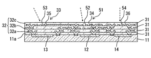
- the light receiving unit 10 is a photodiode having a PN junction, and is formed on the formation surface 11 a of the semiconductor substrate 11.
- the light receiving unit 10 includes three light receiving units 12 to 14, and the light receiving ranges (wavelength bands of light that can be detected) of the light receiving units 12 to 14 are different.
- the defining portion 30 includes a light transmissive film 31 having a light transmissive property, a light shielding film 32 having a light shielding property, and an opening 33 formed in the light shielding film 32.
- the light shielding film 32 includes a first film 32a, a second film 32b, and a third film 32c, and is laminated in this order at a predetermined interval above the formation surface 11a (light receiving unit 10).
- the opening 33 has openings 34 to 36 corresponding to the light receiving parts 12 to 14, respectively, and the incident angles of incident light defined by the openings 34 to 36 are different as shown by broken line arrows in FIG. ing. Further, as indicated by broken lines in FIG. 3, the opening areas of the openings 34 to 36 are also different.
- the selection unit 50 shares the light shielding film 32 included in the defining unit 30 and has a slit 51 formed in the shared light shielding film 32. As described above, the first film 32a, the second film 32b, and the third film 32c are stacked above the formation surface 11a at a predetermined interval. The selection unit 50 shares the second film 32b and the third film 32c apart from the formation surface 11a in the light shielding film 32 with the defining unit 30, and slits 51 in the shared second film 32b and third film 32c. Is formed.
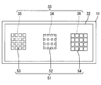
- the slit 51 is located in a region surrounded by the opening 33 and has slits 52 to 54 corresponding to the light receiving portions 12 to 14, respectively.
- the wavelengths of incident light selected by the slits 52 to 54 are different, the first slit 52 selects a wavelength band mainly included in the light irradiated by the light emitting unit 70, and the second slit 53 is a light emitting unit.
- the wavelength band excluding the wavelength band mainly included in the light irradiated at 70 is selected.
- the 3rd slit 54 selects infrared rays.
- the first slit 52 is formed in each of the second film 32b and the third film 32c, and the slits 53 and 54 are formed in the third film 32c.
- a plurality of slits 52 to 54 are formed in the light shielding film 32 in the region surrounded by the opening 33, and the planar shape thereof is rectangular.
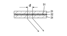
- a filter using surface plasmon resonance is formed by the plurality of slits 51, and the wavelength of incident light to be selected is determined by the filter.
- Surface plasmon exists at the interface between two different substances, and when light having energy that resonates with the surface plasmon, that is, light having a resonating wavelength band is incident on the interface, the surface plasmon resonates with the surface plasmon, and the light intensity becomes stronger. As a result, light with increased intensity is incident on the light receiving unit 10.
- the surface plasmon depends on the physical properties and shape of two substances forming the interface and the distance between the interfaces. Therefore, by changing the substance forming the interface as appropriate, changing the shape of the interface as appropriate, and changing the distance between the interfaces as appropriate, it is possible to select light in a wavelength band that increases the intensity.
- the wavelength that increases the intensity by appropriately changing the materials constituting the light-transmitting film 31 and the light-shielding film 32, appropriately changing the shape of the slit 51, and appropriately changing the interval between the slits 51.
- Band light can be selected.
- the light emitting unit 70 irradiates the front windshield with light and causes the reflected light reflected by the front windshield to enter the first light receiving unit 12.
- the light emitting unit 70 according to the present embodiment is an LED, and the wavelength band of the irradiated light has a longer wavelength than that of visible light.
- the light emitting unit 70 is provided on the semiconductor substrate 11, but may not be provided on the same semiconductor substrate 11 as the light receiving unit 10.
- the light emitting unit 70 may be provided on a different substrate from the light receiving unit 10.
- the storage unit 80 determines the relative positions of the light receiving unit 10 and the front windshield while storing the light receiving unit 10, the defining unit 30, the selection unit 50, and the light emitting unit 70, respectively.
- the storage unit 80 is made of a material that absorbs light emitted from the light emitting unit 70.
- the light receiving unit 10 includes the three light receiving units 12 to 14, the opening 33 of the defining unit 30 includes the three openings 34 to 36, and the slit 51 of the selection unit 50 includes 3 There are two slits 52-54.
- the first light receiving unit 12, the first opening 34, the first slit 52, and the light emitting unit 70 constitute a rain sensor that detects rainfall
- the slit 53 constitutes an angle sensor that detects the incident angle of light incident on the vehicle.
- the third light receiving unit 14, the third opening 36, and the third slit 54 constitute a solar radiation sensor that detects the amount of solar radiation.
- the first light receiving unit 12 corresponds to a light receiving unit for rain sensor
- the second light receiving unit 13 corresponds to a light receiving unit for angle sensor
- the third light receiving unit 14 corresponds to a light receiving unit for solar radiation sensor.
- the defining unit 30 and the selecting unit 50 share the light shielding film 32, and the defining unit 30 has the opening 33 formed in the light shielding film 32.
- a slit 51 made of the film 32 is provided. According to this, an increase in the physique of the optical sensor 100 is suppressed as compared with a configuration in which the defining part and the selecting part are separate.
- the wavelength of incident light selected by the slits 52 to 54 is different. According to this, the light receiving units 12 to 14 can detect light having different wavelengths.
- the first slit 52 corresponding to the first light receiving unit 12 selects a wavelength band mainly included in the light emitted from the light emitting unit 70. According to this, it is suppressed that the light which has wavelength bands other than the wavelength band mainly contained in the light irradiated with the light emission part 70 injects into the 1st light-receiving part 12. FIG. Therefore, the incidence of disturbance light on the first light receiving unit 12 is suppressed, and a decrease in rain detection accuracy is suppressed.
- the second slit 53 corresponding to the second light receiving unit 13 selects a wavelength band excluding the wavelength band mainly included in the light irradiated by the light emitting unit 70. According to this, the light emitted from the light emitting unit 70 is suppressed from entering the second light receiving unit 13. Therefore, a decrease in detection accuracy of the incident angle of light is suppressed.
- the third slit 54 corresponding to the third light receiving unit 14 selects infrared rays. Infrared radiation has the effect of giving heat to the object. Therefore, the temperature rise of the optical sensor 100 due to radiation can be detected by detecting the infrared rays with the third light receiving unit 14.
- the first film 32a, the second film 32b, and the third film 32c are stacked above the formation surface 11a, and an opening 33 is formed in each of the first film 32a, the second film 32b, and the third film 32c. According to this, the incident angle can be narrowed as compared with a configuration in which one light shielding film is stacked above the formation surface and an opening is formed in the light shielding film.
- Each of the defining unit 30 and the selection unit 50 shares the second film 32b and the third film 32c, and the first slit 52 corresponding to the first light receiving unit 12 includes the second film 32b and the third film 32c. Is formed. According to this, compared with the configuration in which the first slit is formed in one light shielding film, the half-value width of the incident light incident on the first light receiving unit 12 is narrowed, and disturbance light is incident on the first light receiving unit 12. It is suppressed. For this reason, the fall of the detection accuracy of rainfall is suppressed.
- the half-value width is the width from the peak value of the incident light intensity to the half value of the peak value.
- the incident angles of the incident light defined by the openings 34 to 36 corresponding to the light receiving units 12 to 14 are different. According to this, light having different incident angles can be detected by each of the light receiving units 12 to 14.
- planar shape of the slit 51 is a rectangle.
- planar shape of the slit 51 is not limited to the above example, and for example, a circle, an ellipse, a polygon, or the like can be adopted.
- a filter using surface plasmon resonance is formed by a plurality of slits 51 formed in the light shielding film 32 in the region surrounded by the opening 33.
- the filter formed by the slit 51 is not limited to the above example.
- a filter using a diffraction grating can be formed by the slit 51.
- the light When light is incident on the diffraction grating, the light is diffracted by the slit 51 constituting the diffraction grating.
- the light diffracted by each slit 51 interferes and the intensity of light of a specific wavelength increases.
- the specific wavelength at which the intensity increases depends on the width d of the slit 51 and the shape of the slit 51. Therefore, by changing the width d of the slit 51 as appropriate and changing the shape of the slit 51 as appropriate, it is possible to select light in a wavelength band that increases the intensity.
- the first film 32a, the second film 32b, and the third film 32c are stacked above the formation surface 11a with a predetermined interval.
- the light shielding film 32 stacked above the formation surface 11a is not limited to the above example. For example, one layer, two layers, or four layers may be used.
- the selection unit 50 shares the second film 32b and the third film 32c apart from the formation surface 11a with the defining unit 30 among the three light shielding films 32 is shown.
- the number to be shared is not limited to the above example and may be one or more layers.
- the wavelengths of incident light selected by the slits 52 to 54 are different is shown.
- the wavelength of the incident light selected by the slits 52 to 54 may not be different.
- the first slit 52 is formed in each of the second film 32b and the third film 32c, and the slits 53 and 54 are formed in the third film 32c.
- the slits 52 to 54 may be formed in at least one of the plurality of light shielding films 32 shared by the selection unit 50 with the defining unit 30.
- the incident angles of incident light defined by the openings 34 to 36 are different.
- the incident angles of the incident light defined by the openings 34 to 36 need not be different.
- the opening areas of the openings 34 to 36 are different.
- the opening areas of the openings 34 to 36 need not be different.
- the light receiving unit 10 includes the light receiving units 12 to 14
- the number of light receiving parts is not limited to the above example.
- a light sensor 100 includes a rain sensor, an angle sensor, and a solar radiation sensor.
- the sensor configured by the optical sensor 100 is not limited to the above example. Further, the number of sensors configured is not limited to the above example.
Landscapes
- Physics & Mathematics (AREA)
- General Physics & Mathematics (AREA)
- Spectroscopy & Molecular Physics (AREA)
- Life Sciences & Earth Sciences (AREA)
- Environmental & Geological Engineering (AREA)
- Engineering & Computer Science (AREA)
- Atmospheric Sciences (AREA)
- Biodiversity & Conservation Biology (AREA)
- Ecology (AREA)
- Environmental Sciences (AREA)
- Hydrology & Water Resources (AREA)
- Chemical & Material Sciences (AREA)
- Optics & Photonics (AREA)
- Analytical Chemistry (AREA)
- Biochemistry (AREA)
- General Health & Medical Sciences (AREA)
- Immunology (AREA)
- Pathology (AREA)
- Health & Medical Sciences (AREA)
- Photometry And Measurement Of Optical Pulse Characteristics (AREA)
- Solid State Image Pick-Up Elements (AREA)
- Light Receiving Elements (AREA)
- Photo Coupler, Interrupter, Optical-To-Optical Conversion Devices (AREA)
- Spectrometry And Color Measurement (AREA)
- Investigating Or Analysing Materials By Optical Means (AREA)
Priority Applications (3)
| Application Number | Priority Date | Filing Date | Title |
|---|---|---|---|
| US14/406,541 US9166081B2 (en) | 2012-09-07 | 2013-09-05 | Optical sensor |
| DE112013005039.0T DE112013005039B4 (de) | 2012-09-07 | 2013-09-05 | Optischer Sensor |
| CN201380039851.0A CN104508438B (zh) | 2012-09-07 | 2013-09-05 | 光传感器 |
Applications Claiming Priority (2)
| Application Number | Priority Date | Filing Date | Title |
|---|---|---|---|
| JP2012197339A JP5907011B2 (ja) | 2012-09-07 | 2012-09-07 | 光センサ |
| JP2012-197339 | 2012-09-07 |
Publications (1)
| Publication Number | Publication Date |
|---|---|
| WO2014038206A1 true WO2014038206A1 (ja) | 2014-03-13 |
Family
ID=50236835
Family Applications (1)
| Application Number | Title | Priority Date | Filing Date |
|---|---|---|---|
| PCT/JP2013/005270 Ceased WO2014038206A1 (ja) | 2012-09-07 | 2013-09-05 | 光センサ |
Country Status (5)
| Country | Link |
|---|---|
| US (1) | US9166081B2 (enExample) |
| JP (1) | JP5907011B2 (enExample) |
| CN (1) | CN104508438B (enExample) |
| DE (1) | DE112013005039B4 (enExample) |
| WO (1) | WO2014038206A1 (enExample) |
Families Citing this family (5)
| Publication number | Priority date | Publication date | Assignee | Title |
|---|---|---|---|---|
| EP3211453A1 (en) * | 2016-02-26 | 2017-08-30 | ams AG | Optical proximity sensor arrangement and method for producing an optical proximity sensor arrangement |
| WO2018069867A1 (en) * | 2016-10-13 | 2018-04-19 | Six Degrees Space Ltd | Method and apparatus for indoor positioning |
| CN106686215B (zh) * | 2016-12-06 | 2022-03-25 | Oppo广东移动通信有限公司 | 传感器组件以及移动终端 |
| TWI637502B (zh) * | 2017-12-05 | 2018-10-01 | 義明科技股份有限公司 | 光學感測裝置以及光學感測模組 |
| JP2024124181A (ja) * | 2023-03-02 | 2024-09-12 | ローム株式会社 | 光検出装置および光検出システム |
Citations (6)
| Publication number | Priority date | Publication date | Assignee | Title |
|---|---|---|---|---|
| JPH06177416A (ja) * | 1992-12-07 | 1994-06-24 | Nippondenso Co Ltd | 光センサー |
| JP2004198214A (ja) * | 2002-12-18 | 2004-07-15 | Denso Corp | 雨滴および光検出装置 |
| JP2009038352A (ja) * | 2007-07-06 | 2009-02-19 | Canon Inc | 光検出素子及び撮像素子、光検出方法及び撮像方法 |
| JP2011187857A (ja) * | 2010-03-11 | 2011-09-22 | Toshiba Corp | 固体撮像装置 |
| JP2012142514A (ja) * | 2011-01-06 | 2012-07-26 | Denso Corp | 光センサ |
| WO2013015117A1 (ja) * | 2011-07-28 | 2013-01-31 | ソニー株式会社 | 固体撮像素子および撮像システム |
Family Cites Families (19)
| Publication number | Priority date | Publication date | Assignee | Title |
|---|---|---|---|---|
| DE4406398A1 (de) | 1994-02-26 | 1995-08-31 | Bosch Gmbh Robert | Regensensor |
| US5428215A (en) * | 1994-05-27 | 1995-06-27 | Her Majesty The Queen In Right Of Canada, As Represented By Minister Of National Defence Of Her Majesty's Canadian Government | Digital high angular resolution laser irradiation detector (HARLID) |
| DE19933642A1 (de) * | 1999-07-17 | 2001-03-08 | Bosch Gmbh Robert | Lichtempfindliche Sensoreinheit, insbesondere zum automatischen Schalten von Beleuchtungseinrichtungen |
| JP2005233728A (ja) * | 2004-02-18 | 2005-09-02 | Denso Corp | 光センサ装置 |
| JP4772585B2 (ja) | 2006-05-10 | 2011-09-14 | 浜松ホトニクス株式会社 | 光検出器 |
| DE102006040790B4 (de) | 2006-08-31 | 2012-04-26 | Fraunhofer-Gesellschaft zur Förderung der angewandten Forschung e.V. | Reflexkoppler mit integriertem organischen Lichtemitter sowie Verwendung eines solchen Reflexkopplers |
| JP4621270B2 (ja) | 2007-07-13 | 2011-01-26 | キヤノン株式会社 | 光学フィルタ |
| EP2254159A4 (en) * | 2007-12-25 | 2012-06-20 | Seiko Instr Inc | OPTICAL DETECTION ARRANGEMENT AND PICTURE DISPLAY ARRANGEMENT |
| KR101776955B1 (ko) * | 2009-02-10 | 2017-09-08 | 소니 주식회사 | 고체 촬상 장치와 그 제조 방법, 및 전자 기기 |
| JP4973692B2 (ja) * | 2009-05-27 | 2012-07-11 | 株式会社デンソー | 移動体用光センサ装置 |
| JP5077780B2 (ja) * | 2009-07-06 | 2012-11-21 | 株式会社デンソー | 光検出装置 |
| JP2011061133A (ja) * | 2009-09-14 | 2011-03-24 | Zycube:Kk | 半導体イメージセンサとその製造法 |
| US20110068426A1 (en) * | 2009-09-22 | 2011-03-24 | Intersil Americas Inc. | Photodiodes and methods for fabricating photodiodes |
| JP5998426B2 (ja) | 2010-03-05 | 2016-09-28 | セイコーエプソン株式会社 | 光学センサー及び電子機器 |
| EP2400559A1 (de) * | 2010-06-22 | 2011-12-28 | SMA Solar Technology AG | Einstrahlungssensor für solare Lichtintensität |
| WO2012032753A1 (ja) | 2010-09-10 | 2012-03-15 | 株式会社デンソー | 光センサ |
| CN201804019U (zh) * | 2010-09-24 | 2011-04-20 | 浙江美佳机电科技有限公司 | 太阳能风光雨传感器 |
| JP2012222742A (ja) * | 2011-04-13 | 2012-11-12 | Sony Corp | 撮像素子および撮像装置 |
| JP6029266B2 (ja) * | 2011-08-09 | 2016-11-24 | キヤノン株式会社 | 撮像装置、撮像システムおよび撮像装置の製造方法 |
-
2012
- 2012-09-07 JP JP2012197339A patent/JP5907011B2/ja not_active Expired - Fee Related
-
2013
- 2013-09-05 DE DE112013005039.0T patent/DE112013005039B4/de not_active Expired - Fee Related
- 2013-09-05 CN CN201380039851.0A patent/CN104508438B/zh not_active Expired - Fee Related
- 2013-09-05 WO PCT/JP2013/005270 patent/WO2014038206A1/ja not_active Ceased
- 2013-09-05 US US14/406,541 patent/US9166081B2/en not_active Expired - Fee Related
Patent Citations (6)
| Publication number | Priority date | Publication date | Assignee | Title |
|---|---|---|---|---|
| JPH06177416A (ja) * | 1992-12-07 | 1994-06-24 | Nippondenso Co Ltd | 光センサー |
| JP2004198214A (ja) * | 2002-12-18 | 2004-07-15 | Denso Corp | 雨滴および光検出装置 |
| JP2009038352A (ja) * | 2007-07-06 | 2009-02-19 | Canon Inc | 光検出素子及び撮像素子、光検出方法及び撮像方法 |
| JP2011187857A (ja) * | 2010-03-11 | 2011-09-22 | Toshiba Corp | 固体撮像装置 |
| JP2012142514A (ja) * | 2011-01-06 | 2012-07-26 | Denso Corp | 光センサ |
| WO2013015117A1 (ja) * | 2011-07-28 | 2013-01-31 | ソニー株式会社 | 固体撮像素子および撮像システム |
Also Published As
| Publication number | Publication date |
|---|---|
| US9166081B2 (en) | 2015-10-20 |
| DE112013005039B4 (de) | 2022-07-21 |
| US20150179830A1 (en) | 2015-06-25 |
| CN104508438A (zh) | 2015-04-08 |
| JP2014052302A (ja) | 2014-03-20 |
| JP5907011B2 (ja) | 2016-04-20 |
| DE112013005039T5 (de) | 2015-07-30 |
| CN104508438B (zh) | 2016-07-13 |
Similar Documents
| Publication | Publication Date | Title |
|---|---|---|
| CN103196562B (zh) | 包括集成至少一个衍射光栅的封装的红外检测器 | |
| JP5907011B2 (ja) | 光センサ | |
| JP6015034B2 (ja) | 光学センサー及び電子機器 | |
| US20090244711A1 (en) | Imaging filter | |
| US20170289524A1 (en) | Optical System for Collecting Distance Information Within a Field | |
| TWI674395B (zh) | 包含一光柵結構之光感測器模組及光譜儀 | |
| KR20180036757A (ko) | 물질의 비접촉 감지를 위한 레퍼런스 스위치 아키텍처 | |
| CN109923445B (zh) | 具有互补角阻挡区域的光学滤光器 | |
| JP2012137646A5 (enExample) | ||
| JP5538194B2 (ja) | 光学装置及び電子機器 | |
| US9733180B2 (en) | Bolometer with high spectral sensitivity | |
| JP2013002966A (ja) | 非分散型赤外ガスセンサ | |
| JP6401647B2 (ja) | 赤外線センサおよび赤外線センサアレイ | |
| JP2006317244A5 (enExample) | ||
| JP2011117884A (ja) | 分光測定器 | |
| JP2014052302A5 (enExample) | ||
| CN211787124U (zh) | 生物识别成像装置和电子装置 | |
| JP2007201475A (ja) | Euv放射線のための狭帯域透過フィルタ | |
| WO2021039955A1 (ja) | 光電変換素子、撮像素子、および撮像システム | |
| JP7137925B2 (ja) | 放射温度計 | |
| EP3605042B1 (en) | Filter assembly, detector, and method of manufacture of a filter assembly | |
| WO2024004538A1 (ja) | 測定装置、照射装置、及び、バンドパスフィルタ | |
| JP2011506981A5 (enExample) | ||
| JP5757254B2 (ja) | 半導体光素子および半導体光装置 | |
| CN110109128A (zh) | 一种红外发射和探测集成芯片 |
Legal Events
| Date | Code | Title | Description |
|---|---|---|---|
| 121 | Ep: the epo has been informed by wipo that ep was designated in this application |
Ref document number: 13834956 Country of ref document: EP Kind code of ref document: A1 |
|
| WWE | Wipo information: entry into national phase |
Ref document number: 14406541 Country of ref document: US |
|
| NENP | Non-entry into the national phase |
Ref country code: DE |
|
| WWE | Wipo information: entry into national phase |
Ref document number: 1120130050390 Country of ref document: DE Ref document number: 112013005039 Country of ref document: DE |
|
| 122 | Ep: pct application non-entry in european phase |
Ref document number: 13834956 Country of ref document: EP Kind code of ref document: A1 |