WO2014030228A1 - 半導体装置、電子機器及び半導体装置の製造方法 - Google Patents
半導体装置、電子機器及び半導体装置の製造方法 Download PDFInfo
- Publication number
- WO2014030228A1 WO2014030228A1 PCT/JP2012/071208 JP2012071208W WO2014030228A1 WO 2014030228 A1 WO2014030228 A1 WO 2014030228A1 JP 2012071208 W JP2012071208 W JP 2012071208W WO 2014030228 A1 WO2014030228 A1 WO 2014030228A1
- Authority
- WO
- WIPO (PCT)
- Prior art keywords
- semiconductor device
- circuit board
- semiconductor element
- bonding
- semiconductor
- Prior art date
- Legal status (The legal status is an assumption and is not a legal conclusion. Google has not performed a legal analysis and makes no representation as to the accuracy of the status listed.)
- Ceased
Links
Images






Classifications
-
- H—ELECTRICITY
- H10—SEMICONDUCTOR DEVICES; ELECTRIC SOLID-STATE DEVICES NOT OTHERWISE PROVIDED FOR
- H10W—GENERIC PACKAGES, INTERCONNECTIONS, CONNECTORS OR OTHER CONSTRUCTIONAL DETAILS OF DEVICES COVERED BY CLASS H10
- H10W72/00—Interconnections or connectors in packages
- H10W72/071—Connecting or disconnecting
- H10W72/073—Connecting or disconnecting of die-attach connectors
-
- B—PERFORMING OPERATIONS; TRANSPORTING
- B82—NANOTECHNOLOGY
- B82Y—SPECIFIC USES OR APPLICATIONS OF NANOSTRUCTURES; MEASUREMENT OR ANALYSIS OF NANOSTRUCTURES; MANUFACTURE OR TREATMENT OF NANOSTRUCTURES
- B82Y40/00—Manufacture or treatment of nanostructures
-
- H—ELECTRICITY
- H10—SEMICONDUCTOR DEVICES; ELECTRIC SOLID-STATE DEVICES NOT OTHERWISE PROVIDED FOR
- H10W—GENERIC PACKAGES, INTERCONNECTIONS, CONNECTORS OR OTHER CONSTRUCTIONAL DETAILS OF DEVICES COVERED BY CLASS H10
- H10W72/00—Interconnections or connectors in packages
- H10W72/01—Manufacture or treatment
- H10W72/013—Manufacture or treatment of die-attach connectors
- H10W72/01321—Manufacture or treatment of die-attach connectors using local deposition
- H10W72/01323—Manufacture or treatment of die-attach connectors using local deposition in liquid form, e.g. by dispensing droplets or by screen printing
-
- H—ELECTRICITY
- H10—SEMICONDUCTOR DEVICES; ELECTRIC SOLID-STATE DEVICES NOT OTHERWISE PROVIDED FOR
- H10W—GENERIC PACKAGES, INTERCONNECTIONS, CONNECTORS OR OTHER CONSTRUCTIONAL DETAILS OF DEVICES COVERED BY CLASS H10
- H10W72/00—Interconnections or connectors in packages
- H10W72/071—Connecting or disconnecting
- H10W72/073—Connecting or disconnecting of die-attach connectors
- H10W72/07331—Connecting techniques
-
- H—ELECTRICITY
- H10—SEMICONDUCTOR DEVICES; ELECTRIC SOLID-STATE DEVICES NOT OTHERWISE PROVIDED FOR
- H10W—GENERIC PACKAGES, INTERCONNECTIONS, CONNECTORS OR OTHER CONSTRUCTIONAL DETAILS OF DEVICES COVERED BY CLASS H10
- H10W72/00—Interconnections or connectors in packages
- H10W72/071—Connecting or disconnecting
- H10W72/073—Connecting or disconnecting of die-attach connectors
- H10W72/07331—Connecting techniques
- H10W72/07332—Compression bonding, e.g. thermocompression bonding
-
- H—ELECTRICITY
- H10—SEMICONDUCTOR DEVICES; ELECTRIC SOLID-STATE DEVICES NOT OTHERWISE PROVIDED FOR
- H10W—GENERIC PACKAGES, INTERCONNECTIONS, CONNECTORS OR OTHER CONSTRUCTIONAL DETAILS OF DEVICES COVERED BY CLASS H10
- H10W72/00—Interconnections or connectors in packages
- H10W72/071—Connecting or disconnecting
- H10W72/073—Connecting or disconnecting of die-attach connectors
- H10W72/07331—Connecting techniques
- H10W72/07332—Compression bonding, e.g. thermocompression bonding
- H10W72/07333—Ultrasonic bonding, e.g. thermosonic bonding
-
- H—ELECTRICITY
- H10—SEMICONDUCTOR DEVICES; ELECTRIC SOLID-STATE DEVICES NOT OTHERWISE PROVIDED FOR
- H10W—GENERIC PACKAGES, INTERCONNECTIONS, CONNECTORS OR OTHER CONSTRUCTIONAL DETAILS OF DEVICES COVERED BY CLASS H10
- H10W72/00—Interconnections or connectors in packages
- H10W72/071—Connecting or disconnecting
- H10W72/073—Connecting or disconnecting of die-attach connectors
- H10W72/07331—Connecting techniques
- H10W72/07334—Using a reflow oven
-
- H—ELECTRICITY
- H10—SEMICONDUCTOR DEVICES; ELECTRIC SOLID-STATE DEVICES NOT OTHERWISE PROVIDED FOR
- H10W—GENERIC PACKAGES, INTERCONNECTIONS, CONNECTORS OR OTHER CONSTRUCTIONAL DETAILS OF DEVICES COVERED BY CLASS H10
- H10W72/00—Interconnections or connectors in packages
- H10W72/071—Connecting or disconnecting
- H10W72/073—Connecting or disconnecting of die-attach connectors
- H10W72/07351—Connecting or disconnecting of die-attach connectors characterised by changes in properties of the die-attach connectors during connecting
- H10W72/07352—Connecting or disconnecting of die-attach connectors characterised by changes in properties of the die-attach connectors during connecting changes in structures or sizes
-
- H—ELECTRICITY
- H10—SEMICONDUCTOR DEVICES; ELECTRIC SOLID-STATE DEVICES NOT OTHERWISE PROVIDED FOR
- H10W—GENERIC PACKAGES, INTERCONNECTIONS, CONNECTORS OR OTHER CONSTRUCTIONAL DETAILS OF DEVICES COVERED BY CLASS H10
- H10W72/00—Interconnections or connectors in packages
- H10W72/30—Die-attach connectors
- H10W72/321—Structures or relative sizes of die-attach connectors
-
- H—ELECTRICITY
- H10—SEMICONDUCTOR DEVICES; ELECTRIC SOLID-STATE DEVICES NOT OTHERWISE PROVIDED FOR
- H10W—GENERIC PACKAGES, INTERCONNECTIONS, CONNECTORS OR OTHER CONSTRUCTIONAL DETAILS OF DEVICES COVERED BY CLASS H10
- H10W72/00—Interconnections or connectors in packages
- H10W72/30—Die-attach connectors
- H10W72/321—Structures or relative sizes of die-attach connectors
- H10W72/325—Die-attach connectors having a filler embedded in a matrix
-
- H—ELECTRICITY
- H10—SEMICONDUCTOR DEVICES; ELECTRIC SOLID-STATE DEVICES NOT OTHERWISE PROVIDED FOR
- H10W—GENERIC PACKAGES, INTERCONNECTIONS, CONNECTORS OR OTHER CONSTRUCTIONAL DETAILS OF DEVICES COVERED BY CLASS H10
- H10W72/00—Interconnections or connectors in packages
- H10W72/30—Die-attach connectors
- H10W72/331—Shapes of die-attach connectors
-
- H—ELECTRICITY
- H10—SEMICONDUCTOR DEVICES; ELECTRIC SOLID-STATE DEVICES NOT OTHERWISE PROVIDED FOR
- H10W—GENERIC PACKAGES, INTERCONNECTIONS, CONNECTORS OR OTHER CONSTRUCTIONAL DETAILS OF DEVICES COVERED BY CLASS H10
- H10W72/00—Interconnections or connectors in packages
- H10W72/30—Die-attach connectors
- H10W72/331—Shapes of die-attach connectors
- H10W72/332—Plan-view shape, i.e. in top view
-
- H—ELECTRICITY
- H10—SEMICONDUCTOR DEVICES; ELECTRIC SOLID-STATE DEVICES NOT OTHERWISE PROVIDED FOR
- H10W—GENERIC PACKAGES, INTERCONNECTIONS, CONNECTORS OR OTHER CONSTRUCTIONAL DETAILS OF DEVICES COVERED BY CLASS H10
- H10W72/00—Interconnections or connectors in packages
- H10W72/30—Die-attach connectors
- H10W72/331—Shapes of die-attach connectors
- H10W72/334—Cross-sectional shape, i.e. in side view
-
- H—ELECTRICITY
- H10—SEMICONDUCTOR DEVICES; ELECTRIC SOLID-STATE DEVICES NOT OTHERWISE PROVIDED FOR
- H10W—GENERIC PACKAGES, INTERCONNECTIONS, CONNECTORS OR OTHER CONSTRUCTIONAL DETAILS OF DEVICES COVERED BY CLASS H10
- H10W72/00—Interconnections or connectors in packages
- H10W72/30—Die-attach connectors
- H10W72/351—Materials of die-attach connectors
-
- H—ELECTRICITY
- H10—SEMICONDUCTOR DEVICES; ELECTRIC SOLID-STATE DEVICES NOT OTHERWISE PROVIDED FOR
- H10W—GENERIC PACKAGES, INTERCONNECTIONS, CONNECTORS OR OTHER CONSTRUCTIONAL DETAILS OF DEVICES COVERED BY CLASS H10
- H10W72/00—Interconnections or connectors in packages
- H10W72/30—Die-attach connectors
- H10W72/351—Materials of die-attach connectors
- H10W72/352—Materials of die-attach connectors comprising metals or metalloids, e.g. solders
-
- H—ELECTRICITY
- H10—SEMICONDUCTOR DEVICES; ELECTRIC SOLID-STATE DEVICES NOT OTHERWISE PROVIDED FOR
- H10W—GENERIC PACKAGES, INTERCONNECTIONS, CONNECTORS OR OTHER CONSTRUCTIONAL DETAILS OF DEVICES COVERED BY CLASS H10
- H10W72/00—Interconnections or connectors in packages
- H10W72/30—Die-attach connectors
- H10W72/351—Materials of die-attach connectors
- H10W72/353—Materials of die-attach connectors not comprising solid metals or solid metalloids, e.g. ceramics
-
- H—ELECTRICITY
- H10—SEMICONDUCTOR DEVICES; ELECTRIC SOLID-STATE DEVICES NOT OTHERWISE PROVIDED FOR
- H10W—GENERIC PACKAGES, INTERCONNECTIONS, CONNECTORS OR OTHER CONSTRUCTIONAL DETAILS OF DEVICES COVERED BY CLASS H10
- H10W72/00—Interconnections or connectors in packages
- H10W72/50—Bond wires
- H10W72/59—Bond pads specially adapted therefor
-
- H—ELECTRICITY
- H10—SEMICONDUCTOR DEVICES; ELECTRIC SOLID-STATE DEVICES NOT OTHERWISE PROVIDED FOR
- H10W—GENERIC PACKAGES, INTERCONNECTIONS, CONNECTORS OR OTHER CONSTRUCTIONAL DETAILS OF DEVICES COVERED BY CLASS H10
- H10W72/00—Interconnections or connectors in packages
- H10W72/90—Bond pads, in general
-
- H—ELECTRICITY
- H10—SEMICONDUCTOR DEVICES; ELECTRIC SOLID-STATE DEVICES NOT OTHERWISE PROVIDED FOR
- H10W—GENERIC PACKAGES, INTERCONNECTIONS, CONNECTORS OR OTHER CONSTRUCTIONAL DETAILS OF DEVICES COVERED BY CLASS H10
- H10W72/00—Interconnections or connectors in packages
- H10W72/90—Bond pads, in general
- H10W72/941—Dispositions of bond pads
- H10W72/9415—Dispositions of bond pads relative to the surface, e.g. recessed, protruding
-
- H—ELECTRICITY
- H10—SEMICONDUCTOR DEVICES; ELECTRIC SOLID-STATE DEVICES NOT OTHERWISE PROVIDED FOR
- H10W—GENERIC PACKAGES, INTERCONNECTIONS, CONNECTORS OR OTHER CONSTRUCTIONAL DETAILS OF DEVICES COVERED BY CLASS H10
- H10W72/00—Interconnections or connectors in packages
- H10W72/90—Bond pads, in general
- H10W72/951—Materials of bond pads
- H10W72/952—Materials of bond pads comprising metals or metalloids, e.g. PbSn, Ag or Cu
-
- H—ELECTRICITY
- H10—SEMICONDUCTOR DEVICES; ELECTRIC SOLID-STATE DEVICES NOT OTHERWISE PROVIDED FOR
- H10W—GENERIC PACKAGES, INTERCONNECTIONS, CONNECTORS OR OTHER CONSTRUCTIONAL DETAILS OF DEVICES COVERED BY CLASS H10
- H10W74/00—Encapsulations, e.g. protective coatings
- H10W74/01—Manufacture or treatment
- H10W74/012—Manufacture or treatment of encapsulations on active surfaces of flip-chip devices, e.g. forming underfills
-
- H—ELECTRICITY
- H10—SEMICONDUCTOR DEVICES; ELECTRIC SOLID-STATE DEVICES NOT OTHERWISE PROVIDED FOR
- H10W—GENERIC PACKAGES, INTERCONNECTIONS, CONNECTORS OR OTHER CONSTRUCTIONAL DETAILS OF DEVICES COVERED BY CLASS H10
- H10W74/00—Encapsulations, e.g. protective coatings
- H10W74/10—Encapsulations, e.g. protective coatings characterised by their shape or disposition
- H10W74/15—Encapsulations, e.g. protective coatings characterised by their shape or disposition on active surfaces of flip-chip devices, e.g. underfills
-
- H—ELECTRICITY
- H10—SEMICONDUCTOR DEVICES; ELECTRIC SOLID-STATE DEVICES NOT OTHERWISE PROVIDED FOR
- H10W—GENERIC PACKAGES, INTERCONNECTIONS, CONNECTORS OR OTHER CONSTRUCTIONAL DETAILS OF DEVICES COVERED BY CLASS H10
- H10W90/00—Package configurations
- H10W90/701—Package configurations characterised by the relative positions of pads or connectors relative to package parts
- H10W90/731—Package configurations characterised by the relative positions of pads or connectors relative to package parts of die-attach connectors
- H10W90/734—Package configurations characterised by the relative positions of pads or connectors relative to package parts of die-attach connectors between a chip and a stacked insulating package substrate, interposer or RDL
Definitions
- the present invention relates to a semiconductor device, an electronic device, and a method for manufacturing the semiconductor device.
- first to third semiconductor elements a substrate having a conductor pattern formed on the upper surface, and first to third metal particles containing a metal particle paste between the lower surface of the semiconductor element and the upper surface of the conductive pattern.
- a semiconductor device comprising a bonding material layer is described.
- the linear expansion coefficient of the semiconductor element and the linear expansion coefficient of the circuit board are greatly different from each other.
- the semiconductor device disclosed in JP 2012-009703 A when the semiconductor element and the circuit board are thermally deformed due to heat generation of the semiconductor element, the deformation amount of the semiconductor element and the deformation amount of the circuit board are calculated. The difference is likely to increase.
- a semiconductor element having a large calorific value with a surface exceeding 200 ° C. is used, a large thermal stress is applied to the bonding layer for bonding the semiconductor element and the circuit board, and peeling or cracking occurs in the bonding layer. As a result, the bonding force between the semiconductor element and the circuit board may be reduced. As described above, there is room for further improvement in the bonding between the semiconductor element and the circuit board.
- One object of the present invention is to provide a semiconductor device, an electronic apparatus, and a method for manufacturing a semiconductor device, which can suppress a decrease in bonding strength between a semiconductor element and a circuit board.
- a semiconductor element A circuit board electrically connected to the semiconductor element; A bonding layer for bonding the semiconductor element and the circuit board; A semiconductor device including metal fine particles and a plurality of nanorods composed of at least the metal is applied to the bonding layer.
- a printed wiring board A semiconductor device mounted on the printed wiring board, The semiconductor device includes a semiconductor element, A circuit board electrically connected to the semiconductor element; An electronic apparatus including a metal fine particle and a bonding layer that includes at least a plurality of nanorods made of the metal and bonds the semiconductor element and the circuit board is applied.
- a semiconductor element is placed on each bonding material and heated to form a bonded body by bonding metal fine particles in the bonding material;
- a method of manufacturing a semiconductor device including a compressive stress generating step of generating a compressive stress in the combined body is applied.
- the present invention it is possible to provide a semiconductor device, an electronic device, and a method of manufacturing a semiconductor device that can suppress a decrease in bonding strength between a semiconductor element and a circuit board.
- FIG. 4 is a flowchart of a manufacturing method of the semiconductor device. It is explanatory drawing which shows step S1 of the manufacturing method of the same semiconductor device. It is explanatory drawing which shows step S2 of the manufacturing method of the same semiconductor device, Comprising: It is a top view of the same semiconductor device. It is explanatory drawing which shows step S2 of the manufacturing method of the same semiconductor device, Comprising: It is explanatory drawing which shows the side cross section of the same semiconductor device. It is explanatory drawing which shows step S3 of the manufacturing method of the same semiconductor device.
- step S4 of the manufacturing method of the same semiconductor device It is explanatory drawing which shows step S4 of the manufacturing method of the same semiconductor device. It is explanatory drawing which shows step S5 of the manufacturing method of the same semiconductor device. It is explanatory drawing which shows step S6 of the manufacturing method of the same semiconductor device. It is explanatory drawing which shows step S7 of the manufacturing method of the same semiconductor device. It is a SEM photograph which shows the growth of the nanorod of the semiconductor device. It is explanatory drawing which shows step S8 of the manufacturing method of the same semiconductor device. It is a SEM photograph which shows the nanorod of the semiconductor device.
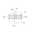
- the semiconductor device 10 is mounted on a printed wiring board 12 as shown in FIG. As illustrated in FIG. 2, the semiconductor device 10 includes a semiconductor element 20, a circuit board 40, and a bonding layer 30.
- the semiconductor element 20 is composed of a semiconductor mainly composed of a group IV single element semiconductor, a group III-V compound semiconductor, a group III-VI compound semiconductor, a group IV-IV compound semiconductor, or the like.
- the semiconductor element 20 is composed of a semiconductor mainly composed of silicon carbide (SiC), which is an IV-IV group compound semiconductor having excellent heat resistance.
- a metal sputter layer 201 such as gold, silver, platinum, copper, or nickel is formed on the circuit board 40 side of the semiconductor element 20.
- the circuit board 40 is electrically connected to the semiconductor element 20.
- the circuit board 40 includes, for example, a lead frame on which a die pad is formed and a DBC (Direct Bonding Copper) board on which a gold plating layer and a nickel plating layer are formed in this order from the surface side.
- DBC Direct Bonding Copper
- the bonding layer 30 can bond the semiconductor element 20 and the circuit board 40.
- the bonding layer 30 includes silver fine particles (an example of metal fine particles) and a plurality of nanorods NL composed of at least silver (an example of metal).
- the particle diameter of silver fine particles (hereinafter simply referred to as “silver fine particles”) is preferably several nanometers to several hundred nanometers.
- the bonding layer may include nickel fine particles and a plurality of nanorods composed of at least nickel.
- the bonding layer may include fine particles of iron and a plurality of nanorods composed of at least iron.
- the bonding layer may include gold-palladium fine particles and a plurality of nanorods composed of at least gold-palladium.
- the bonding layer may include gold-platinum fine particles and a plurality of nanorods composed of at least gold-platinum.
- the bonding layer 30 has a plurality of combined bodies 302 formed by combining silver fine particles.
- Each of the plurality of combined bodies 302 extends in a column shape from the circuit board 40 toward the semiconductor element 20 (from the semiconductor element 20 toward the circuit board 40), and is arranged at intervals.
- the semiconductor element 20 and the circuit board 40 are joined by the plurality of combined bodies 302.
- the plurality of nanorods NL are connected to the adjacent bonded bodies 302, respectively.
- the bonding layer 30 has a bonded body 302 formed by bonding silver fine particles, and at least one nanorod NL is formed of pores 304 formed between the bonded bodies 302. It arrange
- the nanorods NL connect the combined body 302 and the semiconductor element 20 as shown in FIG. Further, among the plurality of nanorods NL, the other nanorods NL2 connect the combined body 302 and the circuit board 40. Furthermore, the nanorods NL may extend from one combined body 302 and stick to other combined bodies 302, or the nanorods NL extended from a plurality of combined bodies 302 may stick to each other.
- the semiconductor device 10 can maintain high bonding strength because the nanorods NL are connected to the bonding bodies 302 in the bonding layer 30. Moreover, since each coupling body 302 is connected with the semiconductor layer 10 via the nanorod NL in the joining layer 30, a bigger electric current can be sent from a viewpoint of a skin effect.
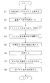
- the semiconductor device 10 is manufactured according to the steps shown in FIG.
- the circuit board 40 shown in FIG. 1 is the aforementioned DBC board 40a.
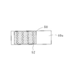
- Step S1 As shown in FIG. 5, a metal mask 50 is placed on the upper surface of the DBC substrate 40a.
- a metal mask 50 In the metal mask 50, a plurality of holes 52 are formed with an interval of, for example, 20 to 50 ⁇ m.
- an optical modeling resin or a rubber mask material may be used.
- a metal nanomaterial (an example of a bonding material) 54 containing silver fine particles, a surface protective material, and a solvent is applied from above the metal mask 50.
- silver fine particles gold fine particles, copper fine particles, platinum fine particles, nickel, gold-palladium, or gold-platinum fine particles may be used.
- Silver fine particles are particles in which silver particles are bonded (for example, low-temperature bonding). As described above, the particle size of the silver fine particles is, for example, several nanometers to several hundred nanometers.
- the surface protective material is, for example, a fatty acid, an alcohol or an amine compound, and a thiol compound.
- Solvents include, for example, paraffinic hydrocarbons such as n-hexane, n-heptane, n-octane, n-nonane and n-decane, higher alcohols such as n-nonanol and n-undecanol, or terpionol, toluene, etc. Is an aromatic hydrocarbon.
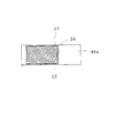
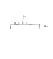
- Step S3 The metal mask 50 is removed, and the DBC substrate 40a is heated in a range of 150 ° C. or less, for example. By the heating, the solvent contained in the metal nanomaterial 54 is evaporated and removed. On the DBC substrate 40a, the metal nanomaterial 54 from which the solvent has been removed remains in a state of being filled in the holes 52 of the metal mask 50 (see FIG. 7). That is, as the arranging step by steps S1 to S3, the metal nanomaterials 54 containing silver fine particles are arranged at a plurality of positions on the DBC substrate 40a with a space therebetween.
- Step S4 As an attaching step, as shown in FIG. 8, a halogen-based organic solvent 56 is sprayed or dropped on the surface of the silver fine particles contained in the metal nanomaterial 54 remaining on the DBC substrate 40a to be attached.
- the halogen-based organic solvent 56 is, for example, one of a halogen-based organic compound, a cationic polymer, a cationic surfactant, and a halogen-based ionic liquid.
- halogen-based organic compounds include chloroform, dichloromethane, carbon tetrachloride, trochloroethylene, tetrachloroethylene, 1,1,1-trichloroethylene, monochlorobenzene, methyl monochloroacetate, ethyl monochloroacetate, methyl bromide, bromochloromethane, and dibromo. Chloromethane, tribromomethane and the like.
- Examples of the cationic polymer include polydiallyldimethylammonium chloride and polyallylamine hydrochloride.
- cationic surfactant examples include dialkyldimethylammonium chloride, distearyldimethylammonium chloride, stearyldimethylzendylammonium chloride, and stearyltrimethylammonium chloride.
- halogen-based ionic liquid examples include 1-ethyl-3-methylimidazolium chloride, 1-ethyl-3-methylimidazolium chloride, 1-butyl-3-methylimidazolium chloride, 1-butyl-2,3 -Dimethylimidazolium chloride, 1-butylpyridinium chloride, tetrabutylammonium chloride, tetrabutylammonium bromide and the like.
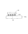
- Step S5 The semiconductor element 20 is left on the DBC substrate 40a in a state where the metal sputtered layer 201 such as gold, silver, platinum, copper, and nickel formed on one side of the semiconductor element 20 faces the DBC substrate 40a. It is placed on the metal nanomaterial 54 (see step S3) including the surface protective material (see FIG. 9).
- the metal sputtered layer 201 such as gold, silver, platinum, copper, and nickel formed on one side of the semiconductor element 20 faces the DBC substrate 40a. It is placed on the metal nanomaterial 54 (see step S3) including the surface protective material (see FIG. 9).
- Step S6 The semiconductor element 20 and the DBC substrate 40a are heated in a heating furnace within a range of 150 to 300 ° C., for example.
- the halogen-based organic solvent 56 see FIG. 8
- the surface protective material are evaporated, and as a forming step, the silver fine particles and the metal sputter layer 201 formed on the semiconductor element 20 are combined.
- silver fine particles are joined to each other by a quantum size effect (for example, low-temperature joining) to form a combined body 302 (see FIG. 10).
- the semiconductor element 20 is electrically connected to the DBC substrate 40a via a plurality of coupling bodies 302 that are spaced apart from each other.
- Step S7 As a compressive stress generation step, subsequent to step S6, heat treatment is performed in the same range of 150 to 300 ° C. to generate a compressive stress on the surface of each combined body 302.
- the heating time is preferably about 48 to 100 hours.
- heating may be performed by ultrasonic irradiation or microwave irradiation.
- the nanorods NL grow from the combined bodies 302 toward the gas phase.
- Step S8 Further, as a voltage application step, a DC pulse voltage is applied between the semiconductor element 20 and the DBC substrate 40a. By introducing this step, the growth of the nanorods NL can be further promoted.
- the semiconductor element 20 and the circuit board 40 are connected through the plurality of combined bodies 302 connected by the nanorods NL.
- the bonding layers 30 are connected to each other through the nanorods NL having elasticity in addition to the bonding between the metal fine particles, the semiconductor device 10 is resistant to repeated thermal expansion. As a result, it is possible to suppress a decrease in the bonding force between the semiconductor element and the circuit board.
- the heat resistance is improved by the above configuration, it is possible to cope with a semiconductor element having a large calorific value such that the surface temperature exceeds 200 ° C., for example.
- the semiconductor element manufacturing method described above can also be applied to a die bonding process for fixing the semiconductor element to the die pad of the lead frame.
- the metal nanomaterial may be arranged on the DBC substrate using a syringe.
- the nanorods may not be included over the entire bonding layer in plan view of the circuit board. That is, the nanorod may be included only in a part of the bonding layer.
Landscapes
- Pressure Welding/Diffusion-Bonding (AREA)
- Die Bonding (AREA)
Abstract
半導体素子20と回路基板40との接合力の低下を抑制することが可能な半導体装置10、電子機器14及び半導体装置10の製造方法を提供する。 半導体装置10は、半導体素子20と、半導体素子20と電気的に接続される回路基板40と、半導体素子20と回路基板40とを接合する接合層30と、を備え、接合層30は、金属の微粒子と、少なくとも金属から構成される複数のナノロッドNLと、を含む。
Description
本発明は、半導体装置、電子機器及び半導体装置の製造方法に関する。
従来、金属粒子を含む導電性ペーストを用いて半導体素子が回路基板に実装された半導体装置が知られている。このような半導体装置は、例えば、特開2012-009703号公報に開示されている。
上記特開2012-009703号公報には、半導体素子と、上面に導体パターンが形成された基板と、半導体素子の下面と導電パターンの上面との間に金属粒子ペーストを含む第1乃至第3の接合材料層とを備えた半導体装置が記載されている。
ここで、一般に、半導体素子の線膨張係数と、回路基板の線膨張係数とは、互いに大きく異なっている。このため、上記特開2012-009703号公報に開示された半導体装置では、半導体素子の発熱によって半導体素子及び回路基板が熱変形した場合に、半導体素子の変形量と、回路基板の変形量との差が大きくなると考えられる。特に、表面が200℃を超えるような発熱量の大きい半導体素子が用いられた場合、半導体素子と回路基板とを接合する接合層に大きな熱応力がかかり、接合層に剥離やクラックが発生して、半導体素子と回路基板との接合力が低下する恐れが生じる。
このように、半導体素子と回路基板との接合については、更に改善すべき余地があった。
このように、半導体素子と回路基板との接合については、更に改善すべき余地があった。
本発明の1つの目的は、半導体素子と回路基板との接合力の低下を抑制することが可能な半導体装置、電子機器及び半導体装置の製造方法を提供することである。
上記課題を解決するため、本発明の一の観点によれば、半導体素子と、
前記半導体素子と電気的に接続される回路基板と、
前記半導体素子と前記回路基板とを接合する接合層と、を備え、
前記接合層は、金属の微粒子と、少なくとも前記金属から構成される複数のナノロッドと、を含む半導体装置が適用される。
前記半導体素子と電気的に接続される回路基板と、
前記半導体素子と前記回路基板とを接合する接合層と、を備え、
前記接合層は、金属の微粒子と、少なくとも前記金属から構成される複数のナノロッドと、を含む半導体装置が適用される。
また、他の観点によれば、プリント配線基板と、
前記プリント配線基板に実装された半導体装置と、を備え、
前記半導体装置は、半導体素子と、
前記半導体素子と電気的に接続される回路基板と、
金属の微粒子と、少なくとも前記金属から構成された複数のナノロッドとを含み、前記半導体素子と前記回路基板とを接合する接合層と、を有する電子機器が適用される。
前記プリント配線基板に実装された半導体装置と、を備え、
前記半導体装置は、半導体素子と、
前記半導体素子と電気的に接続される回路基板と、
金属の微粒子と、少なくとも前記金属から構成された複数のナノロッドとを含み、前記半導体素子と前記回路基板とを接合する接合層と、を有する電子機器が適用される。
また、他の観点によれば、回路基板上に間隔を空けて金属微粒子を含む接合材を複数の箇所に配置する配置工程と、
前記複数の箇所に配置された前記接合材に含まれる前記金属微粒子の表面にハロゲン系有機性溶剤を付着させる付着工程と、
前記付着工程を実行した後、前記各接合材の上に半導体素子を載せて加熱し、前記接合材中の金属微粒子を結合させて結合体を形成する形成工程と、
前記結合体に圧縮応力を発生させる圧縮応力発生工程と、を含む半導体装置の製造方法が適用される。
前記複数の箇所に配置された前記接合材に含まれる前記金属微粒子の表面にハロゲン系有機性溶剤を付着させる付着工程と、
前記付着工程を実行した後、前記各接合材の上に半導体素子を載せて加熱し、前記接合材中の金属微粒子を結合させて結合体を形成する形成工程と、
前記結合体に圧縮応力を発生させる圧縮応力発生工程と、を含む半導体装置の製造方法が適用される。
本発明によれば、半導体素子と回路基板との接合力の低下を抑制することが可能な半導体装置、電子機器及び半導体装置の製造方法を提供できる。
以下、実施の形態を図面に基づいて説明する。なお、各図において、説明に関連しない部分は図示を省略する場合がある。
本実施の形態に係る半導体装置10は、図1に示すように、プリント配線基板12に実装され、電子機器14の一部を構成する。半導体装置10は、図2に示すように、半導体素子20、回路基板40、及び接合層30を備えている。
半導体素子20は、IV族単元素半導体、III-V族化合物半導体、III-VI族化合物半導体、又はIV-IV族化合物半導体などを主成分とする半導体により構成されている。以下では、半導体素子20が耐熱性に優れたIV-IV族化合物半導体の炭化ケイ素(SiC)を主成分とする半導体により構成されているものとして説明する。
半導体素子20の回路基板40の側には、金、銀、白金、銅、ニッケル等の金属スパッタ層201が形成されている。
半導体素子20の回路基板40の側には、金、銀、白金、銅、ニッケル等の金属スパッタ層201が形成されている。
回路基板40は、半導体素子20と電気的に接続される。回路基板40には、例えば、ダイパッドが形成されたリードフレームや、表面側から順に金めっき層及びニッケルめっき層が形成されたDBC(Direct Bonding Copper)基板も含まれる。
接合層30は、半導体素子20と回路基板40とを接合できる。接合層30は、銀の微粒子(金属の微粒子の一例)と、少なくとも銀(金属の一例)から構成される複数のナノロッドNLと、を含んでいる。銀の微粒子(以下、単に「銀微粒子」という。)の粒径は、数ナノ~数百ナノメートルであることが好ましい。
なお、接合層は、ニッケルの微粒子と、少なくともニッケルから構成される複数のナノロッドと、を含んでいてもよい。また、接合層は、鉄の微粒子と、少なくとも鉄から構成される複数のナノロッドと、を含んでいてもよい。また、接合層は、金-パラジウムの微粒子と、少なくとも金-パラジウムから構成される複数のナノロッドと、を含んでいてもよい。また、接合層は、金-白金の微粒子と、少なくとも金-白金から構成される複数のナノロッドと、を含んでいてもよい。
具体的には、接合層30は、銀微粒子が結合してそれぞれ形成された複数の結合体302を有している。これら複数の結合体302は、それぞれ回路基板40から半導体素子20に向かって(半導体素子20から回路基板40に向かって)柱状に延び、互いに間隔を空けて配置されている。半導体素子20及び回路基板40は、これら複数の結合体302によって接合されている。複数のナノロッドNLは、それぞれ隣り合う結合体302に繋がっている。
別の観点から説明すると、接合層30は、銀微粒子が結合して形成された結合体302を有し、少なくとも1本のナノロッドNLが、各結合体302の間に形成された空孔304の内部を通って配置され、各結合体302と繋がっている。
複数のナノロッドNLのうち、一部のナノロッドNL1は、図3に示すように、結合体302と半導体素子20とを繋いでいる。また、複数のナノロッドNLのうち、他のナノロッドNL2は、結合体302と回路基板40とを繋いでいる。更に、ナノロッドNLは、1つの結合体302から延びて、他の結合体302にくっ付く場合もあるし、複数の結合体302から延びたナノロッドNL同士がくっ付く場合もある。
このように、半導体装置10は、接合層30にてナノロッドNLが各結合体302を繋いでいるので、高い接合強度を維持できる。また、半導体装置10は、接合層30にてナノロッドNLを介して各結合体302同士が繋がっているので、表皮効果の観点から、より大きな電流を流すことができる。
次に、半導体装置10の製造方法について説明する。この半導体装置10の製造方法は、いわゆるダイボンディング工程に適用できる。
半導体装置10は、図4に示すステップに従って製造される。なお、本製造方法において、図1に示す回路基板40は、前述のDBC基板40aである。
半導体装置10は、図4に示すステップに従って製造される。なお、本製造方法において、図1に示す回路基板40は、前述のDBC基板40aである。
(ステップS1)
図5に示すように、DBC基板40aの上面に、メタルマスク50を載せる。このメタルマスク50には、複数の孔52が、例えば20~50μmの間隔を空けて形成されている。
なお、メタルマスク50に代えて、例えば光造形樹脂やゴムのマスク材としてもよい。
図5に示すように、DBC基板40aの上面に、メタルマスク50を載せる。このメタルマスク50には、複数の孔52が、例えば20~50μmの間隔を空けて形成されている。
なお、メタルマスク50に代えて、例えば光造形樹脂やゴムのマスク材としてもよい。
(ステップS2)
図6Aに示すように、メタルマスク50の上から、銀微粒子、表面保護材、及び溶媒を含む金属ナノ材料(接合材の一例)54を塗布する。なお、銀微粒子に代えて、金の微粒子、銅の微粒子、白金の微粒子、ニッケル、金-パラジウム、又は金-白金の微粒子としても良い。
銀微粒子は、銀の粒同士が接合(例えば、低温接合)した粒子である。前述の通り、銀微粒子の粒径は、例えば数ナノ~数百ナノメートルである。
表面保護材は、例えば、脂肪酸、アルコールやアミン化合物、及びチオール化合物である。
図6Aに示すように、メタルマスク50の上から、銀微粒子、表面保護材、及び溶媒を含む金属ナノ材料(接合材の一例)54を塗布する。なお、銀微粒子に代えて、金の微粒子、銅の微粒子、白金の微粒子、ニッケル、金-パラジウム、又は金-白金の微粒子としても良い。
銀微粒子は、銀の粒同士が接合(例えば、低温接合)した粒子である。前述の通り、銀微粒子の粒径は、例えば数ナノ~数百ナノメートルである。
表面保護材は、例えば、脂肪酸、アルコールやアミン化合物、及びチオール化合物である。
溶媒は、例えば、n-ヘキサン、n-ヘプタン、n-オクタン、n-ノナン、n-デカン等のパラフィン系炭化水素や、n-ノナノール、n-ウンデカノール等の高級アルコール、又はテルピオネール、トルエンなどの芳香族炭化水素である。
本ステップにより、メタルマスク50に形成された各孔52の内部には、金属ナノ材料54が充填される(図6B参照)。
本ステップにより、メタルマスク50に形成された各孔52の内部には、金属ナノ材料54が充填される(図6B参照)。
(ステップS3)
メタルマスク50を取り除き、DBC基板40aを例えば150℃以下の範囲で加熱する。加熱により、金属ナノ材料54が含む溶媒が蒸発して除去される。DBC基板40aの上には、溶媒が除去された金属ナノ材料54が、メタルマスク50の孔52の内部に充填された状態を保って残る(図7参照)。
つまり、ステップS1~S3による配置工程として、DBC基板40aの上に間隔を空けて銀微粒子を含む金属ナノ材料54が複数の箇所に配置される。
メタルマスク50を取り除き、DBC基板40aを例えば150℃以下の範囲で加熱する。加熱により、金属ナノ材料54が含む溶媒が蒸発して除去される。DBC基板40aの上には、溶媒が除去された金属ナノ材料54が、メタルマスク50の孔52の内部に充填された状態を保って残る(図7参照)。
つまり、ステップS1~S3による配置工程として、DBC基板40aの上に間隔を空けて銀微粒子を含む金属ナノ材料54が複数の箇所に配置される。
(ステップS4)
付着工程として、図8に示すように、DBC基板40aの上に残った金属ナノ材料54に含まれる銀微粒子の表面に、ハロゲン系有機性溶剤56を噴霧又は滴下し、付着させる。
ここで、ハロゲン系有機性溶剤56は、例えば、ハロゲン系有機化合物、カチオン性ポリマー、カチオン性界面活性剤、及びハロゲン系イオン性液体のうちのいずれかである。
付着工程として、図8に示すように、DBC基板40aの上に残った金属ナノ材料54に含まれる銀微粒子の表面に、ハロゲン系有機性溶剤56を噴霧又は滴下し、付着させる。
ここで、ハロゲン系有機性溶剤56は、例えば、ハロゲン系有機化合物、カチオン性ポリマー、カチオン性界面活性剤、及びハロゲン系イオン性液体のうちのいずれかである。
ハロゲン系有機化合物は、例えば、クロロホルム、ジクロロメタン、四塩化炭素、トロクロロエチレン、テトラクロロエチレン、1,1,1-トリクロロエチレン、モノクロロベンゼン、モノクロロ酢酸メチル、モノクロロ酢酸エチル、臭化メチル、ブロモクロロメタン、ジブロモクロロメタン、及びトリブロモメタン等である。
カチオン性ポリマーは、例えば、ポリジアリルジメチルアンモニウムクロリド、及びポリアリルアミン塩酸塩等である。
カチオン性界面活性剤は、例えば、塩化ジアルキルジメチルアンモニウム、塩化ジステアリルジメチルアンモニウム、塩化ステアリルジメチルゼンジルアンモニウム、及び塩化ステアリルトリメチルアンモニウム等である。
ハロゲン系イオン性液体は、例えば、1-エチル-3-メチルイミダゾリウムクロライド、1-エチル-3-メチルイミダソリウムクロライド、1-ブチル-3-メチルイミダゾリウムクロライド、1-ブチル-2,3-ジメチルイミダゾリウムクロライド、1-ブチルピリジウムクロライド、テトラブチルアンモニウムクロリド、及びテトラブチルアンモニウムブロマイド等である。
(ステップS5)
半導体素子20の一方の側に形成された、金、銀、白金、銅、ニッケル等の金属スパッタ層201をDBC基板40aの側に向けた状態で、半導体素子20をDBC基板40aの上に残った表面保護材を含む金属ナノ材料54(ステップS3参照)の上に載せる(図9参照)。
半導体素子20の一方の側に形成された、金、銀、白金、銅、ニッケル等の金属スパッタ層201をDBC基板40aの側に向けた状態で、半導体素子20をDBC基板40aの上に残った表面保護材を含む金属ナノ材料54(ステップS3参照)の上に載せる(図9参照)。
(ステップS6)
半導体素子20及びDBC基板40aを、加熱炉にて、例えば150~300℃の範囲内で加熱する。加熱により、ハロゲン系有機性溶剤56(図8参照)及び表面保護材が蒸発し、形成工程として、銀微粒子と、半導体素子20に形成された金属スパッタ層201とが結合される。一方で、銀微粒子同士は、量子サイズ効果により接合(例えば、低温接合)して、結合体302が形成される(図10参照)。
この結果、半導体素子20は、互いに間隔を空けて配置された複数の結合体302を介してDBC基板40aに電気的に接続される。
なお、本ステップS6においては、加熱するとともに、半導体素子20をDBC基板40aの方向に向かって、例えば0.01~20MPaの範囲内で加圧することが好ましい。
半導体素子20及びDBC基板40aを、加熱炉にて、例えば150~300℃の範囲内で加熱する。加熱により、ハロゲン系有機性溶剤56(図8参照)及び表面保護材が蒸発し、形成工程として、銀微粒子と、半導体素子20に形成された金属スパッタ層201とが結合される。一方で、銀微粒子同士は、量子サイズ効果により接合(例えば、低温接合)して、結合体302が形成される(図10参照)。
この結果、半導体素子20は、互いに間隔を空けて配置された複数の結合体302を介してDBC基板40aに電気的に接続される。
なお、本ステップS6においては、加熱するとともに、半導体素子20をDBC基板40aの方向に向かって、例えば0.01~20MPaの範囲内で加圧することが好ましい。
(ステップS7)
圧縮応力発生工程として、ステップS6に引き続き、同様の150~300℃の範囲で加熱処理を施し、各結合体302の表面に圧縮応力を発生させる。なお、加熱時間は、48~100時間程度が好ましい。この加熱処理においては、超音波照射やマイクロ波照射により加熱しても良い。
この結果、図11及び図12に示すように、各結合体302からナノロッドNLが気相中に向かって成長する。
圧縮応力発生工程として、ステップS6に引き続き、同様の150~300℃の範囲で加熱処理を施し、各結合体302の表面に圧縮応力を発生させる。なお、加熱時間は、48~100時間程度が好ましい。この加熱処理においては、超音波照射やマイクロ波照射により加熱しても良い。
この結果、図11及び図12に示すように、各結合体302からナノロッドNLが気相中に向かって成長する。
また、ハロゲン系有機性溶剤56(図8参照)から遊離した塩素イオンCl-が結合体302の特定の結晶面に付着することにより、その結晶面の成長が抑制される。結果的に、銀微粒子から形成されたナノロッドNLの成長が促進されるので、長いナノロッドNLが形成される。そして、各結合体302から延びて互いに接触していたナノロッドNLが繋がり、図13及び図14に示すように、接合層30が形成される。なお、図3に示したナノロッドNL1、NL2についても、それぞれ半導体素子20及びDBC基板40aに接合される。
(ステップS8)
更に、電圧印加工程として、半導体素子20とDBC基板40aとの間にDCパルス電圧を印加する。本工程を導入することにより、ナノロッドNLの成長をさらに促進させることができる。
更に、電圧印加工程として、半導体素子20とDBC基板40aとの間にDCパルス電圧を印加する。本工程を導入することにより、ナノロッドNLの成長をさらに促進させることができる。
このように、半導体素子20及び回路基板40が、ナノロッドNLによって繋がった複数の結合体302を介して接続される。また、接合層30は、金属微粒子同士の接合に加えて、伸縮性のあるナノロッドNLを介して各結合体302同士が繋がっているので、半導体装置10は繰り返しの熱膨張に強くなる。この結果、半導体素子と回路基板との接合力の低下を抑制することができる。また、上記の構成により耐熱性が向上するので、表面の温度が例えば200℃を超えるような発熱量の大きい半導体素子に対応することも可能になる。
なお、本発明は、前述の実施の形態に限定されるものではなく、本発明の要旨を変更しない範囲での変更は可能である。例えば、前述の実施の形態や変形例の一部又は全部を組み合わせて発明を構成する場合も本発明の技術的範囲に含まれる。
前述の半導体素子の製造方法は、半導体素子をリードフレームのダイパッドに固定するためのダイボンディング工程に適用することもできる。
前述の配置工程においては、シリンジを用いて金属ナノ材料をDBC基板の上に配置してもよい。
前述の配置工程においては、シリンジを用いて金属ナノ材料をDBC基板の上に配置してもよい。
ナノロッドは、回路基板を平面視して接合層全体に亘って含まれていなくてもよい。すなわち、ナノロッドは、接合層の一部にのみ含まれていてもよい。
10:半導体装置、12:プリント配線基板、14:電子機器、20:半導体素子、30:接合層、40:回路基板、40a:DBC基板、50:メタルマスク、52:孔、54:金属ナノ材料、56:ハロゲン系有機性溶剤、201:金属スパッタ層、302:結合体、304:空孔、NL:ナノロッド、NL1:ナノロッド、NL2:ナノロッド
Claims (14)
- 半導体素子と、
前記半導体素子と電気的に接続される回路基板と、
前記半導体素子と前記回路基板とを接合する接合層と、を備え、
前記接合層は、金属の微粒子と、少なくとも前記金属から構成される複数のナノロッドと、を含む半導体装置。 - 請求項1記載の半導体装置において、
前記接合層は、前記金属の微粒子が結合してそれぞれ形成され、且つ、互いに間隔を空けて配置された複数の結合体を有し、
それぞれ隣り合う前記結合体は、前記ナノロッドを介して繋がっている半導体装置。 - 請求項1記載の半導体装置において、
前記接合層の内部に空孔が形成され、該空孔の内部に、少なくとも1本の前記ナノロッドが配置されている半導体装置。 - 請求項2記載の半導体装置において、
前記複数のナノロッドのうち、一部の前記ナノロッドが、前記結合体と前記半導体素子とを繋いでいる半導体装置。 - 請求項2又は4記載の半導体装置において、
前記複数のナノロッドのうち、一部の前記ナノロッドが、前記結合体と前記回路基板とを繋いでいる半導体装置。 - 請求項5記載の半導体装置において、
前記複数の結合体が、それぞれ前記回路基板から前記半導体素子に向かって延びている半導体装置。 - 請求項6記載の半導体装置において、
前記半導体素子の前記回路基板の側の面に、金属スパッタ層が形成されている半導体装置。 - 請求項6又は7記載の半導体装置において、
前記回路基板の前記半導体素子の側の面に、金めっき層及びニッケルめっき層が形成されている半導体装置。 - 請求項4~8のいずれか1項に記載の半導体装置において、
前記金属は、銀、ニッケル、及び鉄の少なくともいずれか一つを含む半導体装置。 - プリント配線基板と、
前記プリント配線基板に実装された半導体装置と、を備え、
前記半導体装置は、半導体素子と、
前記半導体素子と電気的に接続される回路基板と、
金属の微粒子と、少なくとも前記金属から構成された複数のナノロッドとを含み、前記半導体素子と前記回路基板とを接合する接合層と、を有する電子機器。 - 回路基板上に間隔を空けて金属微粒子を含む接合材を複数の箇所に配置する配置工程と、
前記複数の箇所に配置された前記接合材に含まれる前記金属微粒子の表面にハロゲン系有機性溶剤を付着させる付着工程と、
前記付着工程を実行した後、前記各接合材の上に半導体素子を載せて加熱し、前記接合材中の金属微粒子を結合させて結合体を形成する形成工程と、
前記結合体に圧縮応力を発生させる圧縮応力発生工程と、を含む半導体装置の製造方法。 - 請求項11記載の半導体装置の製造方法において、
更に、前記半導体素子と前記回路基板との間に電圧を印加する電圧印加工程と、を含む半導体装置の製造方法。 - 請求項11又は12記載の半導体装置の製造方法において、
前記ハロゲン系有機性溶剤は、ハロゲン系有機化合物、カチオン性ポリマー、カチオン性界面活性剤、及びハロゲン系イオン性液体のうちのいずれかである半導体装置の製造方法。 - 請求項11~13のいずれか1項に記載の半導体装置の製造方法において、
前記形成工程にて、前記半導体素子を前記回路基板の方向に向かって加圧する半導体装置の製造方法。
Priority Applications (1)
| Application Number | Priority Date | Filing Date | Title |
|---|---|---|---|
| PCT/JP2012/071208 WO2014030228A1 (ja) | 2012-08-22 | 2012-08-22 | 半導体装置、電子機器及び半導体装置の製造方法 |
Applications Claiming Priority (1)
| Application Number | Priority Date | Filing Date | Title |
|---|---|---|---|
| PCT/JP2012/071208 WO2014030228A1 (ja) | 2012-08-22 | 2012-08-22 | 半導体装置、電子機器及び半導体装置の製造方法 |
Publications (1)
| Publication Number | Publication Date |
|---|---|
| WO2014030228A1 true WO2014030228A1 (ja) | 2014-02-27 |
Family
ID=50149564
Family Applications (1)
| Application Number | Title | Priority Date | Filing Date |
|---|---|---|---|
| PCT/JP2012/071208 Ceased WO2014030228A1 (ja) | 2012-08-22 | 2012-08-22 | 半導体装置、電子機器及び半導体装置の製造方法 |
Country Status (1)
| Country | Link |
|---|---|
| WO (1) | WO2014030228A1 (ja) |
Citations (3)
| Publication number | Priority date | Publication date | Assignee | Title |
|---|---|---|---|---|
| JPH0511265A (ja) * | 1991-07-08 | 1993-01-19 | Koufu Kashio Kk | 異方性導電膜 |
| JP2004165066A (ja) * | 2002-11-14 | 2004-06-10 | Ricoh Co Ltd | 導電性ペースト、その製造方法、およびそれを用いた接合・分離方法 |
| JP2008004651A (ja) * | 2006-06-21 | 2008-01-10 | Hitachi Ltd | 異方性微粒子を用いた接合材料 |
-
2012
- 2012-08-22 WO PCT/JP2012/071208 patent/WO2014030228A1/ja not_active Ceased
Patent Citations (3)
| Publication number | Priority date | Publication date | Assignee | Title |
|---|---|---|---|---|
| JPH0511265A (ja) * | 1991-07-08 | 1993-01-19 | Koufu Kashio Kk | 異方性導電膜 |
| JP2004165066A (ja) * | 2002-11-14 | 2004-06-10 | Ricoh Co Ltd | 導電性ペースト、その製造方法、およびそれを用いた接合・分離方法 |
| JP2008004651A (ja) * | 2006-06-21 | 2008-01-10 | Hitachi Ltd | 異方性微粒子を用いた接合材料 |
Similar Documents
| Publication | Publication Date | Title |
|---|---|---|
| JP5331113B2 (ja) | 実装構造体 | |
| JP5579928B2 (ja) | 半導体装置およびその製造方法 | |
| TWI255466B (en) | Polymer-matrix conductive film and method for fabricating the same | |
| US9362242B2 (en) | Bonding structure including metal nano particle | |
| JP2011521458A (ja) | プリント回路基板の製造方法および使用ならびにプリント回路基板 | |
| JP2010538463A5 (ja) | ||
| JP2011210773A5 (ja) | ||
| TW201325330A (zh) | 配線基板及其製造方法以及半導體裝置 | |
| CN102315138A (zh) | 两个连接配对件低温压力烧结连接的方法及其制造的系统 | |
| CN109844934B (zh) | 用于低温接合的结构和方法 | |
| EP2860737B1 (en) | Bus bar assembly comprising a memory metal composition | |
| JP2011077308A (ja) | 半導体装置の実装方法 | |
| JP5447117B2 (ja) | 電子機器の製造方法 | |
| KR20180016946A (ko) | 기판 고정 장치 및 그 제조방법 | |
| KR101082742B1 (ko) | 프린트 배선판 및 도전 재료 | |
| JP6797018B2 (ja) | ろう材及びこれを用いたセラミック基板 | |
| JP2014110282A (ja) | 金属微粒子含有ペーストを用いる接合方法 | |
| WO2008114434A1 (ja) | 実装基板及びその製造方法と半導体装置及びその製造方法 | |
| JP5704994B2 (ja) | 半導体接合装置 | |
| WO2014030228A1 (ja) | 半導体装置、電子機器及び半導体装置の製造方法 | |
| JP5950409B2 (ja) | 電極埋め込み石英部材及びその製造方法 | |
| JP4979542B2 (ja) | 実装構造体およびその製造方法 | |
| CN106229309A (zh) | 封装基板及其制造方法 | |
| CN109786351A (zh) | 电连接器的加强 | |
| TWI575685B (zh) | 半導體裝置及其製法 |
Legal Events
| Date | Code | Title | Description |
|---|---|---|---|
| 121 | Ep: the epo has been informed by wipo that ep was designated in this application |
Ref document number: 12883209 Country of ref document: EP Kind code of ref document: A1 |
|
| NENP | Non-entry into the national phase |
Ref country code: DE |
|
| 122 | Ep: pct application non-entry in european phase |
Ref document number: 12883209 Country of ref document: EP Kind code of ref document: A1 |
|
| NENP | Non-entry into the national phase |
Ref country code: JP |