WO2014030185A1 - 画素アレイ基板およびそれを備えた放射線検出装置 - Google Patents
画素アレイ基板およびそれを備えた放射線検出装置 Download PDFInfo
- Publication number
- WO2014030185A1 WO2014030185A1 PCT/JP2012/005258 JP2012005258W WO2014030185A1 WO 2014030185 A1 WO2014030185 A1 WO 2014030185A1 JP 2012005258 W JP2012005258 W JP 2012005258W WO 2014030185 A1 WO2014030185 A1 WO 2014030185A1
- Authority
- WO
- WIPO (PCT)
- Prior art keywords
- pixel
- array substrate
- pixel array
- layer
- tft
- Prior art date
- Legal status (The legal status is an assumption and is not a legal conclusion. Google has not performed a legal analysis and makes no representation as to the accuracy of the status listed.)
- Ceased
Links
Images












Classifications
-
- H—ELECTRICITY
- H10—SEMICONDUCTOR DEVICES; ELECTRIC SOLID-STATE DEVICES NOT OTHERWISE PROVIDED FOR
- H10F—INORGANIC SEMICONDUCTOR DEVICES SENSITIVE TO INFRARED RADIATION, LIGHT, ELECTROMAGNETIC RADIATION OF SHORTER WAVELENGTH OR CORPUSCULAR RADIATION
- H10F39/00—Integrated devices, or assemblies of multiple devices, comprising at least one element covered by group H10F30/00, e.g. radiation detectors comprising photodiode arrays
- H10F39/10—Integrated devices
- H10F39/12—Image sensors
- H10F39/18—Complementary metal-oxide-semiconductor [CMOS] image sensors; Photodiode array image sensors
- H10F39/189—X-ray, gamma-ray or corpuscular radiation imagers
-
- H—ELECTRICITY
- H10—SEMICONDUCTOR DEVICES; ELECTRIC SOLID-STATE DEVICES NOT OTHERWISE PROVIDED FOR
- H10D—INORGANIC ELECTRIC SEMICONDUCTOR DEVICES
- H10D86/00—Integrated devices formed in or on insulating or conducting substrates, e.g. formed in silicon-on-insulator [SOI] substrates or on stainless steel or glass substrates
- H10D86/01—Manufacture or treatment
- H10D86/021—Manufacture or treatment of multiple TFTs
- H10D86/0214—Manufacture or treatment of multiple TFTs using temporary substrates
-
- H—ELECTRICITY
- H10—SEMICONDUCTOR DEVICES; ELECTRIC SOLID-STATE DEVICES NOT OTHERWISE PROVIDED FOR
- H10D—INORGANIC ELECTRIC SEMICONDUCTOR DEVICES
- H10D86/00—Integrated devices formed in or on insulating or conducting substrates, e.g. formed in silicon-on-insulator [SOI] substrates or on stainless steel or glass substrates
- H10D86/01—Manufacture or treatment
- H10D86/021—Manufacture or treatment of multiple TFTs
- H10D86/0241—Manufacture or treatment of multiple TFTs using liquid deposition, e.g. printing
-
- H—ELECTRICITY
- H10—SEMICONDUCTOR DEVICES; ELECTRIC SOLID-STATE DEVICES NOT OTHERWISE PROVIDED FOR
- H10F—INORGANIC SEMICONDUCTOR DEVICES SENSITIVE TO INFRARED RADIATION, LIGHT, ELECTROMAGNETIC RADIATION OF SHORTER WAVELENGTH OR CORPUSCULAR RADIATION
- H10F39/00—Integrated devices, or assemblies of multiple devices, comprising at least one element covered by group H10F30/00, e.g. radiation detectors comprising photodiode arrays
- H10F39/011—Manufacture or treatment of image sensors covered by group H10F39/12
- H10F39/016—Manufacture or treatment of image sensors covered by group H10F39/12 of thin-film-based image sensors
Definitions
- the present invention relates to a pixel provided in a flat panel type radiation detector that detects a thin display (for example, a liquid crystal display) or radiation (for example, light such as X-rays, ⁇ -rays, and infrared rays) used in an output device of a computer or a television.
- a thin display for example, a liquid crystal display
- radiation for example, light such as X-rays, ⁇ -rays, and infrared rays
- the present invention relates to an array substrate and a radiation detection apparatus including the same.
- a thin display or a flat panel radiation detector is provided with a capacitor and a thin film transistor for each pixel in a two-dimensional array (two-dimensional matrix).
- the thin film transistor is hereinafter abbreviated as “TFT” as appropriate.
- TFT The configuration and operation of such a TFT will be described by taking a flat panel radiation detector as an example.
- the capacitor 101 accumulates charges according to the intensity of the radiation by the conversion layer 102 that converts the incident radiation into charges.
- the gate electrode of the TFT 103 is connected to the gate line 104 for each column in the horizontal direction, and the gate line 104 is connected to the gate drive circuit 105.
- a data line 106 is connected to each column in the vertical direction on the opposite terminal connected to the capacitor 101 of the TFT 103.
- the gate drive circuit 105 sequentially transmits drive signals to the gate lines 104, whereby the gates of the TFTs 103 are turned on for each horizontal column of the two-dimensional array of pixels. Thereby, the electric charge accumulated in the capacitor 101 is read out. That is, the charge (detection signal) of each pixel is read and an image is acquired.
- Patent Document 1 discloses a manufacturing method in a flat panel radiation detector. First, a transfer material is connected to the stamp. Next, the transfer material is brought into contact with an uncured liquid resin film (adhesive film) to cure the resin film. Then, the transfer material is peeled off from the stamp. Thereby, the transfer material is transferred onto the substrate using the stamp. A wiring is applied to each transfer material transferred by the stamp to constitute the TFT 103.
- the conventional configuration as described above has the following problems.
- the yield when manufacturing the device is poor.
- a TFT is generated by printing a transfer material on a substrate using a stamp as a plate. Since this TFT is fine, it is difficult to accurately print all of the TFT. That is, according to the conventional configuration, TFTs with poor transfer as shown on the left side of FIG. 25 occur when the TFTs are transferred. Such TFTs that fail to transfer do not function at all.
- the right side of FIG. 25 represents the configuration of the X-ray detector incorporating the substrate generated on the left side of FIG.
- each of the detection pixels indicated by the rectangle on the right side of FIG. 25 is configured to cover the corresponding TFT.
- the detection pixel generated on the transfer defective TFT does not operate normally.
- TFT transfer defects reduce the yield of product manufacturing.
- the present invention has been made in view of such circumstances, and an object of the present invention is to provide a pixel array substrate capable of preventing a pixel from being lost even if a malfunctioning TFT occurs during manufacturing. .
- the present invention has the following configuration in order to solve the above-described problems. That is, the pixel array substrate according to the present invention is a pixel array substrate in which pixels each having a semiconductor layer and a pixel electrode are two-dimensionally arranged, and the pixel electrode is the same provided for one pixel electrode.
- the transistor is electrically connected to a transistor including one selected from a plurality of semiconductor layers having a configuration.
- pixels composed of pixel electrodes and transistors are arranged.
- a pixel in which pixel defects are suppressed is provided.
- An array substrate can be provided.
- the main cause of pixel malfunction is that the transistor does not operate at all.
- a pixel can be configured by selecting a transistor that operates completely from a plurality of transistors at the time of manufacturing, so that a pixel array substrate in which malfunction of the pixel is suppressed can be provided.
- the pixel electrode is electrically connected to a capacitor formed by a part of a plurality of semiconductor layers provided for one pixel electrode.
- the pixel electrode is provided so as to cover a plurality of semiconductor layers.
- an insulating layer is provided between a semiconductor layer that does not constitute a pixel and a pixel electrode.
- the pixel array substrate of the present invention can be mounted on a radiation detection apparatus. According to the device provided with the pixel array substrate according to the present invention, it is possible to provide an image with high visibility since pixel loss is suppressed.
- the pixel array substrate according to the present invention has pixels arranged by pixel electrodes and transistors.
- a pixel in which pixel defects are suppressed is provided.
- An array substrate can be provided.
- the main cause of pixel malfunction is that the transistor does not operate at all.
- a pixel can be configured by selecting a transistor that operates completely from a plurality of transistors at the time of manufacturing, so that a pixel array substrate in which malfunction of the pixel is suppressed can be provided.
- FIG. 3 is a plan view illustrating a configuration of a pixel array substrate according to Example 1.
- FIG. 3 is a plan view illustrating a configuration of a pixel array substrate according to Example 1.
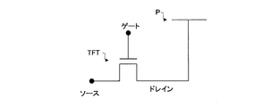
- FIG. 3 is an equivalent circuit diagram of pixels included in the pixel array substrate according to the first embodiment.
- 3 is a flowchart illustrating a manufacturing process of the pixel array substrate according to the first embodiment.
- 6 is a schematic diagram illustrating a method for manufacturing a pixel array substrate according to Example 1.
- FIG. 6 is a schematic diagram illustrating a method for manufacturing a pixel array substrate according to Example 1.
- FIG. 6 is a schematic diagram illustrating a method for manufacturing a pixel array substrate according to Example 1.
- FIG. 6 is a schematic diagram illustrating a method for manufacturing a pixel array substrate according to Example 1.
- FIG. 6 is a schematic diagram illustrating a method for manufacturing a pixel array substrate according to Example 1.
- FIG. 6 is a schematic diagram illustrating a method for manufacturing a pixel array substrate according to Example 1.
- FIG. 6 is a schematic diagram illustrating a method for manufacturing a pixel array substrate according to Example 1.
- FIG. 6 is a schematic diagram illustrating a method for manufacturing a pixel array substrate according to Example 1.
- FIG. 6 is a schematic diagram illustrating a method for manufacturing a pixel array substrate according to Example 1.
- FIG. 6 is a schematic diagram illustrating a method for manufacturing a pixel array substrate according to Example 1.
- FIG. 6 is a schematic diagram illustrating a method for manufacturing a pixel array substrate according to Example 1.
- FIG. 6 is a schematic diagram illustrating a method for manufacturing a pixel array substrate according to Example 1.
- FIG. 6 is a schematic diagram illustrating a method for manufacturing a pixel array substrate according to Example 1.
- FIG. 6 is a schematic diagram illustrating a method for manufacturing a pixel array substrate according to Example 1.
- FIG. 6 is a schematic diagram illustrating a method for manufacturing a pixel array substrate according to Example 1.
- FIG. 6 is a schematic diagram illustrating a configuration of a pixel array substrate according to Example 2.
- FIG. 6 is a schematic diagram illustrating a method for manufacturing a pixel array substrate according to Example 2.
- FIG. 6 is a schematic diagram illustrating a method for manufacturing a pixel array substrate according to Example 2.
- FIG. 6 is a cross-sectional view illustrating a configuration of a radiation detector according to Embodiment 3.
- FIG. 6 is a schematic diagram illustrating a configuration of a radiation detector according to Embodiment 3.
- FIG. It is a schematic diagram explaining the structure which concerns on 1 modification of this invention. It is a schematic diagram explaining a conventional structure. It is a schematic diagram explaining the problem of a conventional structure.
- Embodiment 1 of the present invention will be described below with reference to the drawings.
- a feature of the present invention is that, as shown in FIG. 1, in a pixel array substrate 1 in which pixel electrodes P electrically connected to TFT source or drain terminals are arranged in a two-dimensional matrix, one pixel electrode P is formed.
- islands of a plurality of laminated films 11 are provided (see FIG. 2).
- only one of the islands of the laminated film 11 having the same configuration that functions soundly is selected as a TFT.
- the positional relationship between the pixel electrode P and the island of the laminated film 11 is as follows. That is, the pixel electrode P is configured to straddle the islands of the plurality of stacked films 11.
- the pixel array substrate 1 is configured by two-dimensionally arranging pixels each including a pixel electrode P for accumulating charges and an island of a stacked film 11 electrically connected to the pixel electrode P.
- the pixel is configured by electrically connecting one of the islands of the plurality of stacked films 11 provided for one pixel electrode P to the pixel electrode P.
- the pixel electrode P is provided so as to cover all the islands of the laminated film 11 provided for the pixel electrode P, and the pixel electrode P covers at least the island of the laminated film 11 that does not constitute a pixel. Is provided.
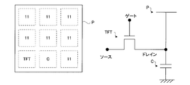
- FIG. 3 shows an equivalent circuit for one pixel in the pixel array substrate 1 of the present invention.
- the pixel array substrate 1 according to the present invention is the same as the conventional device in terms of the circuit. Rather, the feature of the present invention is that each pixel electrode P constituting the pixel has an island of the laminated film 11 that is not actually used as a TFT. These islands of the laminated film 11 do not constitute pixels, and are TFTs discarded in the manufacturing process of the pixel array substrate 1. Since this discarded TFT is not provided with wiring or the like, it does not have a structure that functions as a TFT.
- FIG. 4 will be referred to as appropriate.
- stamp 4 for transfer printing is formed.
- the stamp 4 is made of a flexible material having a good surface releasability, for example, a silicone resin such as PDMS (Polydimethylsiloxane).
- PDMS Polydimethylsiloxane
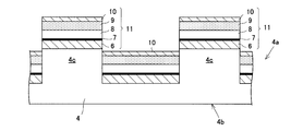
- the stamp 4 is manufactured by coating an original plate 5 having a concavo-convex pattern with a silicone resin and curing it, and then removing it from the original plate 5 as shown in FIG. 6.
- the stamp 4 has a thickness of about 100 ⁇ m to 500 ⁇ m and a front or back side area of about 10 cm square to 100 cm square.
- the height of the concavo-convex portion is about 5 ⁇ m to 50 ⁇ m.
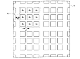
- FIG. 7 shows the stamp 4 viewed from a direction different from that in FIG. That is, the paper surface side in FIG. 7 is the pattern surface 4a of the stamp 4 and corresponds to the lower surface of the stamp 4 described in FIG. That is, FIG. 7 represents a two-dimensional distribution of the convex portions 4 c of the stamp 4.
- the stamp 4 has nine rectangular protrusions 4 c arranged in a 3 ⁇ vertical manner following the rectangular shape to form one convex portion group R.
- the convex group R is arranged in a two-dimensional matrix in the stamp 4.
- a gap having a sufficient width is provided at the boundary of the convex group R. Therefore, the gap d2 provided between the convex part groups R is wider than the gap d1 between two adjacent convex parts 4c among the convex parts 4c belonging to the same convex part group R. .
- Step S2> Formation of Conductive Layer Reference is made to FIG. A conductive layer (metal layer) 6 is formed on the uneven pattern surface 4a of the stamp 4 on which the uneven pattern is formed.
- the conductive layer 6 is formed in contact with the lowermost layer of the laminated film 11 formed in steps S2 to S6, that is, the stamp 4. Thereby, it is possible to easily release the laminated film 11 from the stamp 4 during the transfer in step S7.
- Au is used as the material of the conductive layer 6. Further, the conductive layer 6 is not limited to Au, and other conductive materials may be used as long as the releasability from the stamp 4 is good.
- the conductive layer 6 may be omitted.
- the conductive layer 6 is formed by sputtering, vacuum deposition, ion plating, PECVD, or the like.
- the barrier metal layer 7, the semiconductor layer 8, the insulating film layer 9, and the connection conductive layer 10 formed in steps S3 to S6 are similarly formed by a sputtering method, a vacuum evaporation method, an ion plating method, a PECVD method, or the like.
- a barrier metal layer 7 is formed on the conductive layer 6 formed on the concave / convex pattern surface 4a of the stamp 4.
- the barrier metal layer 7 is provided to improve the adhesion and electrical conductivity between the semiconductor layer 8 and the conductive layer 6 formed in step S4. Further, the barrier metal layer 7 has an effect of preventing metal diffusion and mutual reaction depending on the material of the semiconductor layer 8 and the conductive layer 6.
- Mo mobdenum
- the material of the barrier metal layer 7 is not limited to Mo, and may be Ti (titanium), W (tungsten), or a compound containing them. Further, when the semiconductor layer 8 described later is other than IGZO, the barrier metal layer 7 may not be formed as necessary.
- a semiconductor layer 8 is formed on the barrier metal layer 7 formed on the concave / convex pattern surface 4a of the stamp 4.
- an oxide semiconductor having at least one of In (indium), Ga (gallium), and Zn (zinc), for example, IGZO (InGaZnO 4 ) is used.
- the material of the semiconductor layer 8 may be ZnO (zinc oxide) other than IGZO as an oxide semiconductor.
- the material of the semiconductor layer 8 may be an organic semiconductor such as pentacene, a Si-based semiconductor such as a-Si (amorphous silicon), or a carbon nanotube.
- insulating film layer 9 is formed on the semiconductor layer 8 formed on the concave / convex pattern surface 4a of the stamp 4.
- SiO 2 silicon dioxide
- the material of the insulating film layer 9 is not limited to SiO 2, and may be SiN (silicon nitride), TiO 2 (titanium oxide), Al 2 O 3 (alumina), or PI (polyimide).
- an organic insulating film layer 9 such as an acrylic resin.
- connection Conductive Layer 10 is formed on the insulating film layer 9 formed on the uneven pattern surface 4a of the stamp 4.
- the connection conductive layer 10 is formed on the uppermost layer of the laminated film 11 formed in steps S2 to S6.
- Au is used as the material of the connection conductive layer 10.
- the material of the connection conductive layer 10 is not limited to Au, and may be a conductive material such as Ag.
- the connection conductive layer 10 corresponds to the first conductive layer of the present invention.
- the laminated film 11 is formed on the concave / convex pattern surface 4a of the stamp 4 in the order of the conductive layer 6, the barrier metal layer 7, the semiconductor layer 8, the insulating film layer 9, and the connection conductive layer 10.
- the coated substrate 1h is composed of three layers. That is, the coated substrate 1h has a configuration in which a coated substrate 1ha, a ground layer 1b, and a metal layer 1c are laminated in this order as shown in FIG.
- the material of the coated substrate 1h glass, synthetic resin, Al (aluminum), SUS (stainless steel), graphite, or the like is used.
- PI polyimide
- PEN polyethylene naphthalate
- PES polyether sulfone
- PET polyethylene terephthalate
- the ground layer 1b may be omitted.
- Al is used as the material of the ground layer 1b.
- the material of the ground layer 1b is not limited to Al, and may be a conductive material such as Ni (nickel) or ITO (indium tin oxide).
- Au (gold) is used as the material of the metal layer 1c.
- the material of the metal layer 1c is not limited to Au, and may be a conductive material such as Ag (silver).
- the laminated film 11 of the stamp 4 is transferred to the coated substrate 1h by pressurizing and bonding the stamp 4 from the surface (back surface) 4b opposite to the uneven pattern surface 4a to the coated substrate 1h having such a configuration. .
- Joining is performed by cold welding.
- the uppermost connection conductive layer 10 of the laminated film 11 formed on the stamp 4 and the metal layer 1c formed on the coated substrate 1h face each other.
- the stamp 4 is placed on the coated substrate 1h. Thereby, the connection conductive layer 10 of the stamp 4 and the metal layer 1c of the coating substrate 1h come into contact with each other.
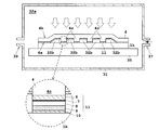
- the back surface 4b of the stamp 4 is pressurized with compressed air (gas).
- compressed air gas
- the coated substrate 1h is supported on the support base 35 in the chamber 31, and the stamp 4 is placed on the coated substrate 1h in a state where the uneven pattern surface 4a of the stamp 4 faces the coated substrate 1h.
- the compressed air is compressed by power such as a pump (not shown) and is supplied from a supply port 37 provided in the chamber 31.
- the compressed air in the chamber 31 is exhausted from the exhaust port 39.
- the compressed air is air or an inert gas such as N 2 (nitrogen) or Ar (argon).
- the space 32a in the chamber 31 is set to 0.4 MPa (4 atm), for example.
- the pressure in the space 32b surrounded by the stamp 4 and the coated substrate 1h is, for example, 0.1 MPa (1 atm).
- the space 32b is sealed with the stamp 4 and the coated substrate 1h. That is, the stamp 4 is pressed against the coating substrate 1h by the pressure difference between the space 32a and the space 32b.
- the inside of the chamber 31 is, for example, normal temperature (20 ⁇ 15 ° C.).
- the state in which the connection conductive layer 10 of the stamp 4 and the metal layer 1c of the coated substrate 1h are in contact, that is, the pressurized state is continued for 6 to 12 hours.
- the pressurization time depends on the pressure and temperature in the chamber 31.
- FIG. 12 shows a state in which the laminated film 11 has been transferred to the coated substrate 1h.
- Both the connection conductive layer 10 of the stamp 4 and the metal layer 1c of the coated substrate 1h are preferably made of Au.
- the Au layer and the Au layer are naturally fused and joined by a preset pressure (for example, 0.4 MPa). Then, after the pressurization time has elapsed, the stamp 4 is separated from the coated substrate 1h, whereby the laminated film 11 is peeled from the stamp 4 and an island of the laminated film 11 is formed on the coated substrate 1h (FIG. 12). reference). This island has a rectangular shape.
- the surfaces of the connection conductive layer 10 of the stamp 4 and the metal layer 1c of the coated substrate 1h may be cleaned by Ar plasma treatment or UV irradiation.
- the islands of the laminated film 11 are arranged in a two-dimensional matrix with the same pattern as described in FIG. 7 on the metal layer 1c side of the coated substrate 1h.
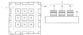
- the left side of FIG. 13 specifically shows this state.
- the symbol r on the left side of FIG. 13 is a transfer group in which the convex portion group R possessed by the stamp 4 is transferred onto the coating substrate 1h.
- islands of the laminated film 11 are arranged in a two-dimensional matrix of 3 ⁇ 3.
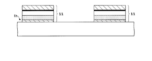
- the right side of FIG. 13 represents a cross section of one transfer group r in the coated substrate 1h.
- the grid-like wiring B is generated so as to avoid the island pattern of the laminated film 11 printed on the coating substrate 1h.
- the grid-like wiring B is printed in a grid shape extending vertically and horizontally on the insulating layer 1d additionally applied on the coated substrate 1h (see the left side of FIG. 14).
- the wiring that extends vertically is a data wiring through which a signal indicating data passes
- the wiring that extends and prints horizontally is a gate wiring through which a signal for controlling the TFT passes.
- An insulating layer is provided at the intersection so as to be sandwiched between the wirings so that the gate wiring and the data wiring are not short-circuited.
- the grid-like wiring B is formed by printing metal ink such as Ag or Cu (copper) with an ink jet printer (ink jet method).
- the printing method is not limited to the ink jet method, and a relief printing method, an intaglio printing method such as gravure printing, a lithographic printing method such as offset printing, a screen printing method, or the like may be used.
- the metal ink is cured by standing at room temperature, heating, or UV irradiation.
- the insulating layer at the intersection and the insulating layer 1d are preferably organic insulating films such as polyimide, and may be applied by various printing methods such as an ink jet method as well as metal wiring. .
- the grid-like wiring B is provided in the gap of the transfer group r. Since the width of the gap of the transfer group r is sufficiently wide, the grid-like wiring B can be easily attached.
- the right side of FIG. 14 represents a cross section of one transfer group r in the coated substrate 1h. Therefore, the lattice-like wiring B has a structure including a plurality of transfer groups r and extends over one surface of the coating substrate 1h.
- Step S9 Selection of Laminated Film
- a method of observing nine islands of the transfer group r with a microscope and selecting islands that are normally transcribed without any defects in the shape is adopted. This selection is performed for all transfer groups r on the coated substrate 1h. In the following description, the following description will be made on the assumption that the island located at the center of the nine islands on the left side of FIG. 13 is selected as the TFT. The remaining islands are discarded TFTs.
- a plurality of islands of the laminated film 11 having the same configuration are generated in the transfer group r by the stamp 4 and one of these is selected to be used as a TFT.
- This island may be selected by visual inspection using an optical camera or by inspection using an electron beam.
- the selection of this island is performed for all the transfer groups r on the coated substrate 1h, and the selection result is stored in a memory included in the inspection apparatus. Based on this information, a TFT described later is generated.
- Step S10> Generation of TFT processing is performed so that the island of the selected laminated film 11 functions as a TFT.
- a part of the conductive layer 6 is cut out of each layer constituting the laminated film 11.
- the barrier metal layer 7 is also etched away to expose the semiconductor layer 8.
- a gate insulating film is formed so as to cover the semiconductor layer 8.
- a lead-in line b is routed from the grid-like wiring B toward the island (selected island) of the laminated film 11, and a TFT is generated.
- These lead lines b are arranged in the gaps between the islands so as not to short-circuit with unselected islands in the transfer group r.
- the one connected to the gate insulating film formed in step S10 is the gate electrode in the TFT, and the other is the source electrode.
- the material and generation method of the lead-in line b are the same as the generation method of the grid-like wiring B described above.
- the right side of FIG. 15 represents a cross section of one transfer group r in the coated substrate 1h. Then, as shown on the right side of FIG. 15, a drain electrode d to be connected to the pixel electrode P in the future is formed.
- the insulating layer 12 is formed so as to cover all the islands of the laminated film 11 included in the transfer group r.
- the insulating layer 12 is formed so as to be accommodated in a section of the grid-like wiring B arranged in a grid.
- the insulating layer 12 is provided with a window w from which the drain electrode d formed in step S10 is exposed. This window w will later be filled with a conductor and will serve as one terminal of the TFT.
- the right side of FIG. 16 represents a cross section of one transfer group r in the coated substrate 1h.
- the pixel electrodes P are laminated on the upper surface of the insulating layer 12.
- the pixel electrode P and the TFT are electrically connected through a conductor filled in the window w.
- the TFT can control the conductivity between the pixel electrode P and the source electrode according to the control state of the gate.
- the right side of FIG. 17 represents a cross section of one transfer group r in the coated substrate 1h.
- the pixel array substrate 1 has pixels arranged by the pixel electrodes P and the TFTs.
- the pixel electrodes P and the TFTs if one of the plurality of TFTs provided for one pixel electrode P and the pixel electrode P are configured to be electrically connected, pixel defects are suppressed.
- a pixel array can be provided.
- the main cause of pixel malfunction is that the TFT does not operate at all.
- a pixel can be configured by selecting all of the TFTs that operate from the plurality of TFTs at the time of manufacturing, so that it is possible to provide the pixel array substrate 1 in which pixel malfunction is suppressed.
- a discarded TFT that does not constitute a pixel is provided so as to cover it, the space on the substrate occupied by the pixel can be saved. Then, since pixels can be arranged with higher density, a higher-performance pixel array substrate 1 can be provided.
- a pixel is not configured.
- the pixel electrode P The pixel array substrate 1 can be provided which ensures insulation from the TFT and operates reliably.
- Example 2 will be described.
- the pixel electrodes P are arranged in a two-dimensional matrix like the configuration of the first embodiment (see FIG. 1). Also in the configuration of the second embodiment, as in the configuration of the first embodiment, a plurality of stacked film 11 islands are provided for one pixel electrode P. The point that one TFT is provided for the pixel electrode P is the same as in the first embodiment.
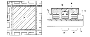
- a feature of the present embodiment that is different from the configuration of Embodiment 1 is that a capacitor C is provided for one pixel electrode P as shown on the left side of FIG. That is, in the configuration of the second embodiment, one of the islands of the laminated film 11 discarded as the TFT functions as the capacitor C.
- the right side of FIG. 18 represents an equivalent circuit for one pixel in the pixel array substrate 1 of the present embodiment.
- the pixel array substrate 1 in this embodiment is the same as the conventional device in terms of the circuit. Rather, the feature of the present invention is that each pixel electrode P constituting the pixel has an island of the laminated film 11 that is not actually used as a TFT, and one of these is used as a capacitor C. It is in.
- the drain of the pixel of the second embodiment is connected to the ground via a capacitor C.
- the manufacturing method according to the second embodiment is similar to the manufacturing method of the pixel array substrate 1 described in the first embodiment. That is, the manufacturing method according to the second embodiment takes the same manufacturing process as that of the first embodiment from step S1 to step S10 described in FIG. Therefore, hereinafter, the production process of the insulating layer, which is a unique configuration in the second embodiment, will be described.
- the capacitor C is also selected when determining which island of the stacked film 11 included in the transfer group r is to be used as the TFT. That is, in step 9, another island for the capacitor is selected in addition to the island used as the TFT.
- the insulating layer 12 is formed so as to cover all the islands of the laminated film 11 included in the transfer group r.
- the insulating layer 12 is formed so as to be accommodated in a section of the grid-like wiring B arranged in a grid.
- the insulating layer 12 is provided with a window w1 in which the drain electrode d formed in step S10 is exposed, and a window w2 in which a part of the upper surface of the laminated film 11 that will function as the capacitor C is exposed in the future.
- This window w1 will be filled with a conductor later and will serve as one terminal of the TFT, and the window w2 will be filled with a conductor later and will serve as one terminal of the capacitor C.
- the right side of FIG. 19 represents a cross section of one transfer group r in the coated substrate 1h.
- the ground layer 1b and the metal layer 1c which are omitted in the description of the manufacturing process of the first embodiment are drawn there.
- the island of the laminated film 11 can be considered as a capacitor C having a predetermined electric capacity. This is because the laminated film 11 has a structure in which the insulating film layer 9 is sandwiched between conductor layers. Moreover, the connection conductive layer 10 is connected to the ground layer 1b through the metal layer 1c. Therefore, the laminated film 11 is a capacitor in which one end of the terminal is connected to the ground.
- the pixel electrodes P are laminated on the upper surface of the insulating layer 12.
- the pixel electrode P and the TFT are electrically connected through a conductor filled in the window w1
- the pixel electrode P and the capacitor C are electrically connected through a conductor filled in the window w2.
- the right side of FIG. 20 represents a cross section of one transfer group r in the coated substrate 1h.
- the charge accumulated in the capacitor C can be handled as a signal, so that the pixel array substrate 1 with an enhanced electrical signal can be provided.
- the configuration of the third embodiment is a configuration in which the pixel array substrate described in the first embodiment is applied to an X-ray detector.
- the X-ray detector 20 includes an array in which detection pixels including a capacitor that detects carriers and accumulates charges and a TFT that controls extraction of the accumulated charges are arranged.
- the pixel array substrate 1 according to Example 1 an amorphous selenium layer 21 that converts X-rays into carrier pairs, a second high-resistance film 22, a common electrode 23 for placing the amorphous selenium layer 21 in an electric field, and a room temperature curing type
- An epoxy resin layer 25 formed by curing an epoxy resin, an auxiliary plate 26 formed of glass, and a first high resistance film 27 are provided.
- the X-ray detector 20 is laminated in the order of the pixel array substrate 1, the first high resistance film 27, the amorphous selenium layer 21, the second high resistance film 22, the common electrode 23, the epoxy resin layer 25, and the auxiliary plate 26. It becomes the composition.
- the amorphous selenium layer 21 corresponds to the conversion layer of the present invention
- the common electrode 23 corresponds to the electrode layer of the present invention.
- the pixel array substrate 1 corresponds to the pixel array substrate of the present invention.
- the amorphous selenium layer 21 is made of high-purity amorphous selenium having a specific resistance of 10 9 ⁇ cm or more (preferably 10 11 ⁇ cm or more).
- the thickness in the stacking direction is 0.2 mm to 2 mm.
- a collecting electrode (pixel electrode P) for collecting carriers is formed on a glass substrate.
- the pixel electrodes P are in contact with the first high resistance film 27 and are two-dimensionally arranged on the surface of the pixel array substrate 1.
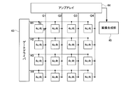
- the pixel electrode P is connected to a charge extraction TFT as shown in FIG.
- this TFT has a gate G for current control and a read electrode S for reading a detection signal. When the gate G of the TFT is turned on, the charge induced in the pixel electrode P flows toward the readout electrode S.
- the two-dimensionally arranged TFTs are connected to wiring extending in a grid pattern in the vertical and horizontal directions. That is, the readout electrodes S of the TFTs arranged in the vertical direction in FIG. 22 are all connected to one of the common amplifier electrodes Q1 to Q4, and the gates G of the TFTs arranged in the horizontal direction in FIG. Are connected to any one of the gate control electrodes H1 to H4.
- the gate control electrodes H1 to H4 are connected to the gate driver 43, and the amplifier electrodes Q1 to Q4 are connected to the amplifier array 44.
- the pixel array substrate 1 has a two-dimensional array of pixels including capacitors C, TFTs, and gates G.
- the gate driver 43 controls the potential of the gate electrode G that turns on and off the TFT.
- a configuration for reading out the electric charge accumulated in each capacitor C will be described. It is assumed that charges are accumulated in each of the capacitors C in FIG.
- the gate driver 43 turns on the TFTs all at once through the gate control electrode H1.
- the four TFTs arranged side by side transmit charges (original signals) to the amplifier array 44 through the amplifier electrodes Q1 to Q4.
- the gate driver 43 turns on the TFTs all at once through the gate control electrode H2. In this way, the gate driver 43 turns on the gate control electrodes H1 to H4 in order. Each time, the TFTs arranged in one line are turned on all at once.
- the X-ray detector 20 is configured to read out the electric charge accumulated in each capacitor C for each row.
- an amplifier for amplifying a signal is provided for each of the amplifier electrodes Q1 to Q4.
- the original signals input to the amplifier array 44 from the amplifier electrodes Q1 to Q4 are amplified here with a predetermined amplification factor.
- the image generation unit 45 generates an X-ray fluoroscopic image based on the original signal output from the amplifier array 44.
- the pixel electrode P, the capacitor C, and the TFT constitute an X-ray detection pixel that detects X-rays.
- the X-ray detection pixels form a two-dimensional matrix, for example, 3,072 ⁇ 3,072 arranged vertically and horizontally on the pixel array substrate 1.
- the common electrode 23 is made of gold and is provided for the purpose of applying a bias voltage to the amorphous selenium layer 21 via the second high resistance film 22. As shown in FIG. 21, it is connected to the node 23a. By supplying a high potential to the node 23a, a positive bias voltage of 10 kV, for example, is applied to the common electrode 23 as a potential.
- the first high resistance film 27 and the second high resistance film 22 are made of, for example, Sb 2 S 3 and are films that selectively pass either electrons or holes.
- the film thickness is about 0.1 ⁇ m to 5 ⁇ m, and the specific resistance is 10 9 ⁇ cm or more.
- the first high resistance film 27 is a high resistance layer that rectifies current flowing from the amorphous selenium layer 21 to the pixel array substrate 1.
- the second high resistance film 22 is also provided for the purpose of rectifying the current flowing through the common electrode 23 and the amorphous selenium layer 21.
- the present invention is not limited to the above embodiment, and can be modified as follows.
- the transfer group r in Example 1 has a configuration in which nine islands of the laminated film 11 are arranged, but the present invention is not limited to this. In the present invention, the arrangement of the islands of the laminated film 11 belonging to the transfer group r can be freely selected.
- the concave / convex pattern surface 4a of the stamp 4 can be freely changed in accordance with the setting change of the transfer group r.
- the present invention is not limited to this.
- the gap between the transfer groups r may be configured to coincide with the arrangement pitch of the islands of the laminated film 11 inside the transfer group r. That is, the islands of the laminated film 11 of this modification are arranged at an equal pitch over the entire surface of the coated substrate 1h and cannot be discriminated apparently. By doing so, the generation of the stamp 4 can be made simpler.
- the islands of the laminated film 11 in Example 1 may be generated by etching the coated substrate 1h, not limited to letterpress printing and transfer printing, but also intaglio printing methods such as gravure printing, A planographic printing method such as offset printing, a screen printing method, offset printing, inkjet printing, or the like may be used.
- the pixel array substrate 1 can be generated by using a mask method for a wide range of film formation, and by using an ink jet printing method for forming fine wirings and wirings. . In this way, the pixel array substrate 1 can be generated quickly and accurately.
- step S10 the lead-in line b is disposed in the gap between the islands of the insulating layer 12, but the present invention is not limited to this configuration.
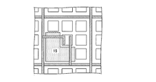
- an insulating layer 15 may be formed so as to cover an unselected island in the transfer group r, and a lead-in line b may be generated on the upper surface thereof.
- step S9 only a plurality of islands of the laminated film 11 in the transfer group r can be selected and function as TFTs. In this way, one of the TFTs can be used for controlling the capacitor C, and the other can be used for signal amplification.
- the pixel array substrate 1 of the present invention can also be mounted on an image display device. According to the device provided with the pixel array substrate according to the present invention, it is possible to provide an image display device with high visibility since pixel defects are suppressed.
- the present invention is suitable for a radiation imaging apparatus.
Landscapes
- Solid State Image Pick-Up Elements (AREA)
Description
本発明は、コンピュータの出力装置やテレビなどに用いられる薄型ディスプレイ(例えば液晶ディスプレイ)や放射線(例えばX線やγ線や赤外線等の光)を検出するフラットパネル型放射線検出器に設けられる、画素アレイ基板およびそれを備えた放射線検出装置に関する。
従来、薄型ディスプレイやフラットパネル型放射線検出器には、二次元アレイ状(二次元マトリクス状)の画素ごとにコンデンサと薄膜トランジスタ(thin film transistor)が設けられている。なお、薄膜トランジスタは、以下適宜「TFT」と略されるものとする。このようなTFTについて、フラットパネル型放射線検出器を一例に構成および動作を説明する。
図24を参照する。まず、コンデンサ101には、入射した放射線を電荷に変換する変換層102により、放射線の強度に応じた電荷が蓄積される。TFT103のゲート電極は、水平方向の列ごとにゲート線104が接続され、ゲート線104は、ゲート駆動回路105に接続されている。また、TFT103のコンデンサ101と接続される反対側の端子には、垂直方向の列ごとにデータ線106が接続されている。ゲート駆動回路105は、ゲート線104に順次、駆動信号を発信することにより、二次元アレイ状の画素の水平方向の列ごとにTFT103のゲートがON状態になる。これにより、コンデンサ101に蓄積された電荷が読み出される。すなわち各画素の電荷(検出信号)を読み出して、画像を取得している。
特許文献1には、フラットパネル型放射線検出器における製造方法が開示されている。まず、スタンプに転写材料を接続させる。次に、その転写材料を硬化されていない液体状の樹脂膜(接着膜)に接触させ、樹脂膜を硬化させる。そして、転写材料をスタンプから剥離する。これにより、スタンプを用いて基板上に転写材料を転写させている。このスタンプで転写された転写材料の各々に配線が施されてTFT103が構成される。
しかしながら、上述のような従来構成によれば、次のような問題点がある。
すなわち、従来構成によれば、装置を製造するときの歩留まりが悪いのである。
すなわち、従来構成によれば、装置を製造するときの歩留まりが悪いのである。
従来構成によれば、スタンプを版として転写材料を基板上に印刷することでTFTが生成される。このTFTは、微細なので、TFTの全てを正確に印刷するのは難しい。つまり、従来構成によれば、TFTを転写した時点で図25左側に示すような転写不良のTFTが発生してしまう。このような転写に失敗したTFTは、全うに機能はしない。
図25右側は、図25左側で生成された基板を組み込んだX線検出器の構成を表している。従来構成によれば、TFTと検出画素とが1対1で対応しているので、図25右側の矩形で示す検出画素のそれぞれは、対応するTFTを覆うように構成される。このとき、基板上にTFTの転写不良が発生していると、転写不良のTFTの上に生成された検出画素は、正常に動作することがない。
つまり、従来の製造方法では、TFTの転写不良が発生すると、それがそのまま画素の欠損を引き起こしてしまう。TFTの転写不良は、スタンプを用いた方法では、必ずある程度は起こってしまうので、転写不良に由来する画素の欠損は、無視できない頻度で起こりえる。
あまりにTFTの転写不良が多い基板は、製品として用いることができない。つまり、従来構成によれば、TFTの転写不良が製品製造の歩留まりを低下させてしまっている。
本発明は、この様な事情に鑑みてなされたものであって、その目的は、製造時に動作不良のTFTが生じても画素が欠損をすることを防止できる画素アレイ基板を提供することにある。
本発明は上述の課題を解決するために次のような構成をとる。
すなわち、本発明に係る画素アレイ基板は、半導体層と画素電極とを備えた画素が2次元的に配列された画素アレイ基板であって、画素電極は、1つの画素電極に対し設けられた同一構成を有している複数の半導体層のうちから選択された1つにより構成されたトランジスタと電気的に接続されていることを特徴とするものである。
すなわち、本発明に係る画素アレイ基板は、半導体層と画素電極とを備えた画素が2次元的に配列された画素アレイ基板であって、画素電極は、1つの画素電極に対し設けられた同一構成を有している複数の半導体層のうちから選択された1つにより構成されたトランジスタと電気的に接続されていることを特徴とするものである。
[作用・効果]本発明に係る画素アレイ基板は、画素電極とトランジスタとで構成される画素が配列されている。この様な構成において、1つの画素電極に対して設けられた複数のトランジスタのうちの1つと画素電極とが電気的に接続されて構成されるようにすれば、画素の欠損が抑制された画素アレイ基板が提供できる。画素が動作不良を起こすのは、トランジスタが全うに動作しないことが主な原因である。本発明の構成では、複数のトランジスタのうちから全うに動作するものを製造時に選んで画素を構成することができるので、画素の動作不良が抑制された画素アレイ基板が提供できる。
また、上述の画素アレイ基板において、画素電極は、1つの画素電極に対し設けられた複数の半導体層の一部により構成されたコンデンサと電気的に接続されていればより望ましい。
[作用・効果]上述の構成は、本発明のより具体的な構成を示すものとなっている。画素の各々にコンデンサを設ける構成とすれば、コンデンサに蓄積された電荷を信号として扱うことができるので電気信号が強化された画素アレイ基板が提供できる。
また、上述の画素アレイ基板において、画素電極は、複数の半導体層を覆うように設けられていればより望ましい。
[作用・効果]上述の構成は、本発明のより具体的な構成を示すものとなっている。上述のように複数の半導体層を覆うように設けられていれば、画素が占める基板上のスペースを節約することができる。すると、画素をより高密度に配列することができるので、より高性能な画素アレイ基板が提供できる。
また、上述の画素アレイ基板において、画素を構成しない半導体層と画素電極との間には絶縁層が備えられていればより望ましい。
[作用・効果]上述の構成は、本発明のより具体的な構成を示すものとなっている。上述のように複数のトランジスタに跨って積層された絶縁層を備え、画素を構成しない、いわば廃棄されたトランジスタと、画素電極との電気的な絶縁性を確保すれば画素電極とトランジスタとの絶縁性が担保され、確実に動作する画素アレイ基板が提供できる。
本発明の画素アレイ基板は、放射線検出装置に搭載することができる。本発明に係る画素アレイ基板を備える装置によれば、画素の欠損が抑制されるので、視認性の高い画像を提供できる。
本発明に係る画素アレイ基板は、画素電極とトランジスタとで構成される画素が配列されている。この様な構成において、1つの画素電極に対して設けられた複数のトランジスタのうちの1つと画素電極とが電気的に接続されて構成されるようにすれば、画素の欠損が抑制された画素アレイ基板が提供できる。画素が動作不良を起こすのは、トランジスタが全うに動作しないことが主な原因である。本発明の構成では、複数のトランジスタのうちから全うに動作するものを製造時に選んで画素を構成することができるので、画素の動作不良が抑制された画素アレイ基板が提供できる。
以降、本発明を実施する形態について実施例を参照して説明する。
以下、図面を参照して本発明の実施例1を説明する。本発明の特徴は、図1に示すように、TFTのソースもしくはドレイン端子と電気的に接続された画素電極Pが2次元マトリックス状に配列された画素アレイ基板1において、1つの画素電極Pに対して複数の積層膜11の島が設けられている点にある(図2参照)。しかも、これら同一構成を有している積層膜11の島のうち、健全に機能するものが1つだけ選択されTFTとされているのである。画素電極Pと積層膜11の島との位置関係は次の通りである。すなわち、画素電極Pは、複数の積層膜11の島に跨るように構成されている。画素電極Pに被覆されている積層膜11の島のうち、画素電極Pと電気的に接続されているものは、1つしかなく、その他の積層膜11の島は、絶縁膜によって画素電極Pと電気的に絶縁されている。この画素電極Pと積層膜11の島とが電気的に接続されて、一つの画素を形成するのである。
従って、本発明に係る画素アレイ基板1は、電荷を蓄積する画素電極Pと、画素電極Pに電気的に接続された積層膜11の島を備えた画素が2次元的に配列されて構成される。そして、画素は、1つの画素電極Pに対して設けられた複数の積層膜11の島のうちの1つと画素電極Pとが電気的に接続されて構成されているのである。この画素電極Pは、これに対して設けられた積層膜11の島の全てを覆うように設けられており、画素電極Pは、このうち少なくとも画素を構成しない積層膜11の島を覆うように設けられている。
図3は、本発明の画素アレイ基板1における画素一つ分の等価回路を表している。図3を参照すれば分かるように、本発明における画素アレイ基板1は回路上は従来装置と同様である。むしろ本発明の特徴は、画素を構成する画素電極Pの各々について、実際にTFTとして使用されなかった積層膜11の島を有している点である。これら積層膜11の島は、画素を構成せず、画素アレイ基板1の製造工程において、いわば廃棄されたTFTとなっている。この廃棄されたTFTは、配線などが施されていないので、TFTとして機能する構造を有していない。
まず、図4のフローチャートに沿って画素アレイ基板の製造方法を説明する。以降、適宜図4を参照する。
<ステップS1>スタンプの形成
まず、転写印刷用のスタンプ4が形成される。スタンプ4は、柔軟性があり表面の離型性のよい材料、例えばPDMS(Polydimethylsiloxane)などのシリコーン樹脂で構成される。スタンプ4は、図5に示すように、凹凸パターンを有する原版5にシリコーン樹脂をコーティングして硬化させ、図6に示すように、原版5から剥離することで作製される。スタンプ4は、例えば、厚みが100μm~500μm程で、前面または背面側の面積が10cm角~100cm角程度の大きさである。また凹凸部の高さは、約5μm~50μm程である。
まず、転写印刷用のスタンプ4が形成される。スタンプ4は、柔軟性があり表面の離型性のよい材料、例えばPDMS(Polydimethylsiloxane)などのシリコーン樹脂で構成される。スタンプ4は、図5に示すように、凹凸パターンを有する原版5にシリコーン樹脂をコーティングして硬化させ、図6に示すように、原版5から剥離することで作製される。スタンプ4は、例えば、厚みが100μm~500μm程で、前面または背面側の面積が10cm角~100cm角程度の大きさである。また凹凸部の高さは、約5μm~50μm程である。
このとき生成されるスタンプ4の構成についてより具体的に説明する。図7は、スタンプ4を図6とは別の方向から見ている。すなわち、図7における紙面表面側がスタンプ4のパターン面4aであり、図6で説明したスタンプ4の下側面に相当する。すなわち、図7は、スタンプ4の凸部4cの2次元的な分布を表している。図7を見れば分かるように、スタンプ4には、9個の矩形の凸部4cが矩形状に倣って縦3×横3に配列され、1つの凸部群Rが形成されている。そして、この凸部群Rは、スタンプ4において、2次元マトリックス状に配列されている。凸部群Rの境界には十分な幅の隙間が設けられている。したがって、同一の凸部群Rに属する凸部4cのうち隣接する2つの凸部4cの間の隙間d1よりも、凸部群R同士の間に設けられた隙間d2の方が広くなっている。
<ステップS2>導電層の形成
図8を参照する。凹凸パターンが形成されたスタンプ4の凹凸パターン面4aに導電層(金属層)6を形成する。ステップS2~S6で形成される積層膜11の最下層、すなわち、スタンプ4に接して導電層6を形成する。これにより、ステップS7の転写時の際に、スタンプ4から積層膜11を離型させ易くすることができる。導電層6の材料は、Auが用いられる。また、導電層6は、Auに限定されず、スタンプ4との離型性が良ければ他の導電性材料を用いてもよい。また、例えば、ステップS3で形成されるバリアメタル層7がスタンプ4との離型性が良いときは、導電層6を省略してもよい。導電層6は、スパッタリング法、真空蒸着法、イオンプレーティング法、PECVD法等で形成される。なお、ステップS3~S6で形成されるバリアメタル層7,半導体層8,絶縁膜層9,接続導電層10も同様に、スパッタリング法、真空蒸着法、イオンプレーティング法、PECVD法等で形成される。
図8を参照する。凹凸パターンが形成されたスタンプ4の凹凸パターン面4aに導電層(金属層)6を形成する。ステップS2~S6で形成される積層膜11の最下層、すなわち、スタンプ4に接して導電層6を形成する。これにより、ステップS7の転写時の際に、スタンプ4から積層膜11を離型させ易くすることができる。導電層6の材料は、Auが用いられる。また、導電層6は、Auに限定されず、スタンプ4との離型性が良ければ他の導電性材料を用いてもよい。また、例えば、ステップS3で形成されるバリアメタル層7がスタンプ4との離型性が良いときは、導電層6を省略してもよい。導電層6は、スパッタリング法、真空蒸着法、イオンプレーティング法、PECVD法等で形成される。なお、ステップS3~S6で形成されるバリアメタル層7,半導体層8,絶縁膜層9,接続導電層10も同様に、スパッタリング法、真空蒸着法、イオンプレーティング法、PECVD法等で形成される。
<ステップS3>バリアメタル層の形成
スタンプ4の凹凸パターン面4aに形成された導電層6上にバリアメタル層7を形成する。バリアメタル層7は、ステップS4で形成される半導体層8と導電層6との間における密着性および導電率を良くするために設けられる。さらにバリアメタル層7は、半導体層8や導電層6の材料により、金属拡散防止や相互反応防止の効果を有する。バリアメタル層7の材料は、後述する半導体層8がIGZOの場合、Mo(モリブデン)が用いられる。また、バリアメタル層7の材料は、Moに限定されず、Ti(チタン),W(タングステン)等、またはそれらを含む化合物であってもよい。また、後述する半導体層8がIGZO以外の場合は、必要に応じてバリアメタル層7を形成しなくともよい。
スタンプ4の凹凸パターン面4aに形成された導電層6上にバリアメタル層7を形成する。バリアメタル層7は、ステップS4で形成される半導体層8と導電層6との間における密着性および導電率を良くするために設けられる。さらにバリアメタル層7は、半導体層8や導電層6の材料により、金属拡散防止や相互反応防止の効果を有する。バリアメタル層7の材料は、後述する半導体層8がIGZOの場合、Mo(モリブデン)が用いられる。また、バリアメタル層7の材料は、Moに限定されず、Ti(チタン),W(タングステン)等、またはそれらを含む化合物であってもよい。また、後述する半導体層8がIGZO以外の場合は、必要に応じてバリアメタル層7を形成しなくともよい。
<ステップS4>半導体層の形成
スタンプ4の凹凸パターン面4aに形成されたバリアメタル層7上に半導体層8を形成する。半導体層8の材料は、In(インジウム),Ga(ガリウム),Zn(亜鉛)を少なくとも1つを有する酸化物半導体、例えばIGZO(InGaZnO4)が用いられる。また、半導体層8の材料は、酸化物半導体としてIGZO以外にも、ZnO(酸化亜鉛)であってもよい。また、半導体層8の材料は、ペンタセン等の有機半導体、a-Si(アモルファスシリコン)等のSi系の半導体、あるいはカーボンナノチューブであってもよい。
スタンプ4の凹凸パターン面4aに形成されたバリアメタル層7上に半導体層8を形成する。半導体層8の材料は、In(インジウム),Ga(ガリウム),Zn(亜鉛)を少なくとも1つを有する酸化物半導体、例えばIGZO(InGaZnO4)が用いられる。また、半導体層8の材料は、酸化物半導体としてIGZO以外にも、ZnO(酸化亜鉛)であってもよい。また、半導体層8の材料は、ペンタセン等の有機半導体、a-Si(アモルファスシリコン)等のSi系の半導体、あるいはカーボンナノチューブであってもよい。
<ステップS5>絶縁層の形成
スタンプ4の凹凸パターン面4aに形成された半導体層8上に絶縁膜層9を形成する。絶縁膜層9の材料は、SiO2(二酸化ケイ素)が用いられる。また、絶縁膜層9の材料は、SiO2に限定されず、SiN(窒化シリコン)や、TiO2(酸化チタン),Al2O3(アルミナ),であってもよく、また、PI(ポリイミド)やアクリル系樹脂等の有機系の絶縁膜層9であってもよい。
スタンプ4の凹凸パターン面4aに形成された半導体層8上に絶縁膜層9を形成する。絶縁膜層9の材料は、SiO2(二酸化ケイ素)が用いられる。また、絶縁膜層9の材料は、SiO2に限定されず、SiN(窒化シリコン)や、TiO2(酸化チタン),Al2O3(アルミナ),であってもよく、また、PI(ポリイミド)やアクリル系樹脂等の有機系の絶縁膜層9であってもよい。
<ステップS6>接続導電層の形成
スタンプ4の凹凸パターン面4aに形成された絶縁膜層9上に接続導電層(金属層)10を形成する。ステップS2~S6で形成される積層膜11の最上層に接続導電層10を形成する。接続導電層10の材料は、Auが用いられる。また、接続導電層10の材料は、Auに限定されず、Ag等の導電性材料であってもよい。なお、接続導電層10は、本発明の第1導電層に相当する。
スタンプ4の凹凸パターン面4aに形成された絶縁膜層9上に接続導電層(金属層)10を形成する。ステップS2~S6で形成される積層膜11の最上層に接続導電層10を形成する。接続導電層10の材料は、Auが用いられる。また、接続導電層10の材料は、Auに限定されず、Ag等の導電性材料であってもよい。なお、接続導電層10は、本発明の第1導電層に相当する。
ステップS2~S6により、スタンプ4の凹凸パターン面4aには、導電層6,バリアメタル層7,半導体層8,絶縁膜層9,接続導電層10の順番で積層膜11が形成される。
<ステップS7>転写
次に、スタンプ4のパターン面4aに成膜された積層膜11を被膜基板1hに写し取る転写を行う。この被膜基板1hは、3つの層から構成されている。すなわち、被膜基板1hは、図9に示すように被膜基板1haと、グランド層1bと金属層1cとがこの順に積層された構成となっている。
次に、スタンプ4のパターン面4aに成膜された積層膜11を被膜基板1hに写し取る転写を行う。この被膜基板1hは、3つの層から構成されている。すなわち、被膜基板1hは、図9に示すように被膜基板1haと、グランド層1bと金属層1cとがこの順に積層された構成となっている。
被膜基板1hの材料は、ガラス、合成樹脂、Al(アルミニウム),SUS(ステンレス)およびグラファイト等が用いられる。合成樹脂の場合は、PI(ポリイミド),PEN(ポリエチレンナフタレート),PES(ポリエーテルスルホン),PET(ポリエチレンテレフタレート)等が用いられる。なお、例えばAl,SUSやグラファイト等の導電性材料で被膜基板1hが構成される場合は、グランド層1bを省略してもよい。
グランド層1bの材料は、例えばAlが用いられる。このグランド層1bの材料は、Alに限定されず、Ni(ニッケル)やITO(酸化インジウムスズ)等の導電性材料であってもよい。金属層1cの材料は、Au(金)が用いられる。また、金属層1cの材料は、Auに限定されず、Ag(銀)等の導電性材料であってもよい。
このような構成の被膜基板1hに前記凹凸パターン面4aの反対側の面(背面)4bからスタンプ4を気体で加圧して接合させることにより、被膜基板1hにスタンプ4の積層膜11を転写する。接合は低温溶接(cold welding)で行われる。図10に示すように、スタンプ4に形成された積層膜11の最上層の接続導電層10と、被膜基板1hに形成された金属層1cとが対向する状態とする。次に、スタンプ4を被膜基板1hに載置させる。これにより、スタンプ4の接続導電層10と被膜基板1hの金属層1cとが接触する。
スタンプ4を被膜基板1hに載置した後、図11に示すように、圧縮空気(気体)によりスタンプ4の背面4bを加圧する。具体的には、被膜基板1hは、チャンバ31内の支持台35に支持しておき、スタンプ4の凹凸パターン面4aを被膜基板1hに対向した状態で、スタンプ4が被膜基板1hに載置されている。圧縮空気は、図示しないポンプ等の動力により圧縮されて、チャンバ31内に設けられた供給口37から供給される。なお、チャンバ31内の圧縮空気は、排気口39から排気するようになっている。圧縮空気は、大気あるいは、N2(窒素)やAr(アルゴン)等の不活性ガスが用いられる。加圧は、チャンバ31内の空間32aを、例えば0.4MPa(4気圧)にする。一方、スタンプ4と被膜基板1hとで囲まれた空間32bの圧力が、例えば0.1MPa(1気圧)であるとする。なお、空間32bは、スタンプ4と被膜基板1hとで密閉されている。すなわち、これら空間32aと空間32bとの圧力差によりスタンプ4が被膜基板1hに加圧される。チャンバ31内は、例えば常温(20±15℃)である。スタンプ4の接続導電層10と被膜基板1hの金属層1cとが接触した状態、すなわち加圧した状態は、6~12時間継続される。加圧時間は、チャンバ31内の圧力と温度に依存する。図12は、被膜基板1hに積層膜11を転写し終えた状態を表している。
スタンプ4の接続導電層10と被膜基板1hの金属層1cは、共にAuで構成されていることが好ましい。Au層とAu層は、予め設定された圧力(例えば0.4MPa)により、自然に融合して接合される(cold welding)。そして、上述の加圧時間が経過した後、スタンプ4を被膜基板1hから離すことで、スタンプ4から積層膜11が剥離され、被膜基板1h上に積層膜11の島が形成される(図12参照)。この島は矩形の形状をなしている。なお、転写前に、スタンプ4の接続導電層10と被膜基板1hの金属層1cの表面を、Arプラズマ処理やUV照射でクリーニングしてもよい。
この様な操作により、被膜基板1hの金属層1c側には、積層膜11の島が図7で説明したものと同じパターンでもって2次元マトリックス状に配列されることになる。図13左側は、この様子を具体的に表している。図13左側における符号rは、スタンプ4が有していた凸部群Rが被膜基板1h上に転写されたもので転写群と呼ぶことにする。この転写群rの1つ当たりに縦3×横3の2次元マトリックス状に積層膜11の島が配列されている。図13右側は、被膜基板1hにおける1つの転写群rについての断面を表している。
<ステップS8>格子状配線の付設
次に、被膜基板1hに印刷された積層膜11の島のパターンを避けるようにして格子状配線Bを生成する。この格子状配線Bは、被膜基板1h上に追加塗布された絶縁層1d上に、縦横に延伸した格子状に印刷される(図14左側参照)。このうち縦に伸びて印刷される配線はデータを示す信号が通過するデータ配線であり、横に伸びて印刷される配線はTFTを制御する信号が通過するゲート配線である。ゲート配線とデータ配線とはショートしないように、交点部に互いの配線に挟まれるように絶縁層が設けられている。格子状配線Bの材料は、AgまたはCu(銅)等が用いられる。格子状配線Bは、AgまたはCu(銅)等の金属インクをインクジェットプリンタ(インクジェット法)で印刷することにより形成される。また、印刷法は、インクジェット法に限定されず、凸版印刷法や、グラビア印刷等の凹版印刷法、オフセット印刷等の平版印刷法、スクリーン印刷法等を用いてもよい。金属インクは、常温放置、加熱またはUV照射により硬化される。また、前記交差部の絶縁層ならびに、絶縁層1dは、ポリイミドなどの有機系の絶縁膜が好適で、金属配線同様、インクジェット法を初めとする各種印刷方法によって塗布されるものであっても良い。
次に、被膜基板1hに印刷された積層膜11の島のパターンを避けるようにして格子状配線Bを生成する。この格子状配線Bは、被膜基板1h上に追加塗布された絶縁層1d上に、縦横に延伸した格子状に印刷される(図14左側参照)。このうち縦に伸びて印刷される配線はデータを示す信号が通過するデータ配線であり、横に伸びて印刷される配線はTFTを制御する信号が通過するゲート配線である。ゲート配線とデータ配線とはショートしないように、交点部に互いの配線に挟まれるように絶縁層が設けられている。格子状配線Bの材料は、AgまたはCu(銅)等が用いられる。格子状配線Bは、AgまたはCu(銅)等の金属インクをインクジェットプリンタ(インクジェット法)で印刷することにより形成される。また、印刷法は、インクジェット法に限定されず、凸版印刷法や、グラビア印刷等の凹版印刷法、オフセット印刷等の平版印刷法、スクリーン印刷法等を用いてもよい。金属インクは、常温放置、加熱またはUV照射により硬化される。また、前記交差部の絶縁層ならびに、絶縁層1dは、ポリイミドなどの有機系の絶縁膜が好適で、金属配線同様、インクジェット法を初めとする各種印刷方法によって塗布されるものであっても良い。
格子状配線Bは、転写群rの隙間に設けられる。転写群rの隙間の幅は、十分に広いものとなっているので、容易に格子状配線Bを付設することができる。図14右側は、被膜基板1hにおける1つの転写群rについての断面を表している。したがって、格子状配線Bは、複数の転写群rを包含する構造で、被膜基板1hの1面に及んでいる。
<ステップS9>積層膜の選択
次に、転写群rが有する積層膜11の島のうち、どの島をTFTとして使用するかを決定する。この具体的な決定方法としては、顕微鏡で転写群rが有する9つの島を観察して、形状に欠損などが見られず正常に転写がなされている島を選択する方法が採用される。この選択は、被膜基板1hにおける全ての転写群rについて行われる。以下の説明において、図13左側における9つの島のうち中央に位置する島がTFTとして選択されたものとして以降の説明を行う。残りの島は、いわば廃棄されたTFTである。このように、本発明によれば、スタンプ4により同一構成の積層膜11の島を転写群rの中で複数生成し、これらのうちの1つをTFTとして使用するものとして選択する。
次に、転写群rが有する積層膜11の島のうち、どの島をTFTとして使用するかを決定する。この具体的な決定方法としては、顕微鏡で転写群rが有する9つの島を観察して、形状に欠損などが見られず正常に転写がなされている島を選択する方法が採用される。この選択は、被膜基板1hにおける全ての転写群rについて行われる。以下の説明において、図13左側における9つの島のうち中央に位置する島がTFTとして選択されたものとして以降の説明を行う。残りの島は、いわば廃棄されたTFTである。このように、本発明によれば、スタンプ4により同一構成の積層膜11の島を転写群rの中で複数生成し、これらのうちの1つをTFTとして使用するものとして選択する。
この島の選択は、光学カメラを用いた外観検査によってもよいし、電子ビームを用いた検査によってもよい。
この島の選択は、被膜基板1h上の全ての転写群rについて行われ、選択結果は、検査装置が有するメモリーに記憶される。この情報に基づいて後述のTFTの生成が行われる。
<ステップS10>TFTの生成
続いて、選択された積層膜11の島をTFTとして機能するように加工が施される。まず、図14右側に示すように積層膜11を構成する各層のうち、導電層6の一部を削り込む。このとき、バリアメタル層7も同時に削り込まれて、半導体層8を露出させる。そして、半導体層8を被覆するようにゲート絶縁膜を形成させる。
続いて、選択された積層膜11の島をTFTとして機能するように加工が施される。まず、図14右側に示すように積層膜11を構成する各層のうち、導電層6の一部を削り込む。このとき、バリアメタル層7も同時に削り込まれて、半導体層8を露出させる。そして、半導体層8を被覆するようにゲート絶縁膜を形成させる。
そして、図15左側に示すように、格子状配線Bから積層膜11の島(選択された島)に向けて引き込み線bが配線され、TFTが生成される。引き込み線bは2つあり、1つはゲート配線と積層膜11の島とを電気的に接続するものであり、もう1つはデータ配線と積層膜11の島とを電気的に接続するものである。これら引き込み線bは、転写群rにおける選択されていない島とショートすることがないように、島同士の隙間に配設される。積層膜11の島に接続された2つの引き込み線bのうちステップS10で形成されたゲート絶縁膜に接続されたものがTFTにおけるゲート電極となり、もう1つがソース電極となる。引き込み線bの材料及び生成方法は、上述の格子状配線Bの生成方法と同様である。図15右側は、被膜基板1hにおける1つの転写群rについての断面を表している。そして、図15右側に示すように、将来画素電極Pと接続されるドレイン電極dが形成される。
<ステップS11>絶縁層の生成
次に、図16右側に示すように、転写群rが有する積層膜11の島を全て覆うように絶縁層12が形成される。この絶縁層12は、格子状に配置された格子状配線Bの区画に収まるように形成される。この絶縁層12には、ステップS10で形成されたドレイン電極dが露出した窓wが設けられている。この窓wは、後に導体が充填され、TFTの1端子を担うことになる。図16右側は、被膜基板1hにおける1つの転写群rについての断面を表している。
次に、図16右側に示すように、転写群rが有する積層膜11の島を全て覆うように絶縁層12が形成される。この絶縁層12は、格子状に配置された格子状配線Bの区画に収まるように形成される。この絶縁層12には、ステップS10で形成されたドレイン電極dが露出した窓wが設けられている。この窓wは、後に導体が充填され、TFTの1端子を担うことになる。図16右側は、被膜基板1hにおける1つの転写群rについての断面を表している。
<ステップS12>画素電極の積層
次に、図17左側が示すように、絶縁層12の上面上に画素電極Pが積層される。このとき、画素電極PとTFTとは窓wに充填された導電体を通じて電気的に接続される。これにより、TFTは、ゲートの制御状況により、画素電極Pとソース電極との間の伝導性が制御できるのである。図17右側は、被膜基板1hにおける1つの転写群rについての断面を表している。
次に、図17左側が示すように、絶縁層12の上面上に画素電極Pが積層される。このとき、画素電極PとTFTとは窓wに充填された導電体を通じて電気的に接続される。これにより、TFTは、ゲートの制御状況により、画素電極Pとソース電極との間の伝導性が制御できるのである。図17右側は、被膜基板1hにおける1つの転写群rについての断面を表している。
以上のように、本発明に係る画素アレイ基板1は、画素電極PとTFTとで構成される画素が配列されている。この様な構成において、1つの画素電極Pに対して設けられた複数のTFTのうちの1つと画素電極Pとが電気的に接続されて構成されるようにすれば、画素の欠損が抑制された画素アレイが提供できる。画素が動作不良を起こすのは、TFTが全うに動作しないことが主な原因である。本発明の構成では、複数のTFTのうちから全うに動作するものを製造時に選んで画素を構成することができるので、画素の動作不良が抑制された画素アレイ基板1が提供できる。
また、上述のように画素を構成しない廃棄されたTFTを覆うように設けるようにすれば、画素が占める基板上のスペースを節約することができる。すると、画素をより高密度に配列することができるので、より高性能な画素アレイ基板1が提供できる。
上述のように複数のTFTに跨って積層された絶縁層12を備えることにより画素を構成しない、いわば廃棄されたTFTと、画素電極Pとの電気的な絶縁性を確保すれば画素電極PとTFTとの絶縁性が担保され、確実に動作する画素アレイ基板1が提供できる。
続いて実施例2を説明する。実施例2の画素アレイ基板1は、実施例1の構成と同様に画素電極Pが2次元マトリックス状に配列されている(図1参照)。また、実施例2の構成においても、実施例1の構成と同様に1つの画素電極Pに対して複数の積層膜11の島が設けられている。画素電極Pに対して1つのTFTが設けられている点も実施例1と同様である。
実施例1の構成とは異なる本実施例の特徴は、図18左側に示すように1つの画素電極Pに対してコンデンサCが設けられている点にある。すなわち、実施例2の構成においては、TFTとしては廃棄された積層膜11の島のうちの一つがコンデンサCとして機能しているのである。
図18右側は、本実施例の画素アレイ基板1における画素一つ分の等価回路を表している。図18右側を参照すれば分かるように、本実施例における画素アレイ基板1は回路上は従来装置と同様である。むしろ本発明の特徴は、画素を構成する画素電極Pの各々について、実際にTFTとして使用されなかった積層膜11の島を有し、これらのうちの一つをコンデンサCとして使用している点にある。
なお、図3の等価回路図とは異なり、実施例2の画素のドレインは、コンデンサCを介してグラウンドに接続されている。
続いて、実施例2に係る画素アレイ基板1の製造方法について説明する。実施例2に係る製造方法は、実施例1で説明した画素アレイ基板1の製造方法に類似している。すなわち実施例2に係る製造方法は、図4で説明したステップS1~ステップS10まで実施例1と同じ製造過程をとる。したがって、以降、実施例2において特有の構成である絶縁層の生成工程から説明する。ただし、上述したステップ9において、転写群rが有する積層膜11の島のうち、どの島をTFTとして使用するかを決定する際に、コンデンサCについての選択もされている。すなわち、ステップ9において、TFTとして使用する島以外にコンデンサ用の島をもう一つ選択するのである。
<ステップT11>絶縁層の生成
実施例2の構成では、図19左側に示すように、転写群rが有する積層膜11の島を全て覆うように絶縁層12が形成される。この絶縁層12は、格子状に配置された格子状配線Bの区画に収まるように形成される。この絶縁層12には、ステップS10で形成されたドレイン電極dが露出した窓w1と、将来コンデンサCとして機能する積層膜11の上面の一部が露出した窓w2とが設けられている。この窓w1は、後に導体が充填され、TFTの1端子を担うことになり、窓w2は、後に導体が充填されコンデンサCの一端子を担うことになる。図19右側は、被膜基板1hにおける1つの転写群rについての断面を表している。そこには実施例1の製造工程の説明では省略されていたグランド層1bおよび金属層1cとが描かれている。
実施例2の構成では、図19左側に示すように、転写群rが有する積層膜11の島を全て覆うように絶縁層12が形成される。この絶縁層12は、格子状に配置された格子状配線Bの区画に収まるように形成される。この絶縁層12には、ステップS10で形成されたドレイン電極dが露出した窓w1と、将来コンデンサCとして機能する積層膜11の上面の一部が露出した窓w2とが設けられている。この窓w1は、後に導体が充填され、TFTの1端子を担うことになり、窓w2は、後に導体が充填されコンデンサCの一端子を担うことになる。図19右側は、被膜基板1hにおける1つの転写群rについての断面を表している。そこには実施例1の製造工程の説明では省略されていたグランド層1bおよび金属層1cとが描かれている。
積層膜11の島は所定の電気容量を有するコンデンサCと考えることができる。なぜならば、積層膜11は、絶縁膜層9が導体の層で挟まれた構造を有しているからである。しかも、接続導電層10は、金属層1cを介してグランド層1bに接続されている。したがって、積層膜11は、端子の一端がグランドに接続されたコンデンサなのである。
<ステップT12>画素電極の積層
次に、図20左側が示すように、絶縁層12の上面上に画素電極Pが積層される。このとき、画素電極PとTFTとは窓w1に充填された導電体を通じて電気的に接続され、画素電極PとコンデンサCとは窓w2に充填された導電体を通じて電気的に接続される。図20右側は、被膜基板1hにおける1つの転写群rについての断面を表している。
次に、図20左側が示すように、絶縁層12の上面上に画素電極Pが積層される。このとき、画素電極PとTFTとは窓w1に充填された導電体を通じて電気的に接続され、画素電極PとコンデンサCとは窓w2に充填された導電体を通じて電気的に接続される。図20右側は、被膜基板1hにおける1つの転写群rについての断面を表している。
この様な構成とすれば、コンデンサCに蓄積された電荷を信号として扱うことができるので電気信号が強化された画素アレイ基板1が提供できる。
実施例3の構成は、実施例1で説明した画素アレイ基板をX線検出器に応用した構成となっている。
<X線検出器の全体構成>
実施例1に係るX線検出器20は、図21に示すように、キャリアを検出するとともに電荷を蓄積するコンデンサと蓄積した電荷の取り出しを制御するTFTとを備えた検出画素が配列された実施例1に係る画素アレイ基板1と、X線をキャリア対に変換するアモルファスセレン層21と、第2高抵抗膜22と、アモルファスセレン層21を電界に置くための共通電極23と、常温硬化型エポキシ樹脂が硬化して構成されるエポキシ樹脂層25と、ガラスで構成される補助板26と、第1高抵抗膜27とを有している。また、X線検出器20は、画素アレイ基板1,第1高抵抗膜27,アモルファスセレン層21,第2高抵抗膜22,共通電極23,エポキシ樹脂層25,および補助板26の順に積層された構成となっている。アモルファスセレン層21は、本発明の変換層に相当し、共通電極23は、本発明の電極層に相当する。また、画素アレイ基板1は、本発明の画素アレイ基板に相当する。
実施例1に係るX線検出器20は、図21に示すように、キャリアを検出するとともに電荷を蓄積するコンデンサと蓄積した電荷の取り出しを制御するTFTとを備えた検出画素が配列された実施例1に係る画素アレイ基板1と、X線をキャリア対に変換するアモルファスセレン層21と、第2高抵抗膜22と、アモルファスセレン層21を電界に置くための共通電極23と、常温硬化型エポキシ樹脂が硬化して構成されるエポキシ樹脂層25と、ガラスで構成される補助板26と、第1高抵抗膜27とを有している。また、X線検出器20は、画素アレイ基板1,第1高抵抗膜27,アモルファスセレン層21,第2高抵抗膜22,共通電極23,エポキシ樹脂層25,および補助板26の順に積層された構成となっている。アモルファスセレン層21は、本発明の変換層に相当し、共通電極23は、本発明の電極層に相当する。また、画素アレイ基板1は、本発明の画素アレイ基板に相当する。
アモルファスセレン層21は、比抵抗109Ωcm以上(好ましくは1011Ωcm以上)となっている高純度のアモルファスセレンで構成される。その積層方向の厚さは、0.2mm~2mmとなっている。このアモルファスセレン層21にX線が照射されると、正孔と電子のペアであるキャリア対が発生する。アモルファスセレン層21は、強い電場に置かれているので、キャリアは、それに伴って移動し、画素アレイ基板1に形成された画素電極Pに電荷が誘起される。
画素アレイ基板1には、実施例1で説明したように、ガラス基板上にキャリア収集用の収集電極(画素電極P)が形成されている。画素電極Pは、第1高抵抗膜27に接するとともに、画素アレイ基板1の表面に2次元的に配列されている。この画素電極Pは、図21に示すように、電荷取り出し用のTFTに接続されている。このTFTは、画素電極Pに接続される入力端子の他に、電流制御用のゲートGと、検出信号読み出し用の読み出し電極Sとを有している。TFTのゲートGがオンされると、画素電極Pに誘起された電荷は読み出し電極Sに向けて流れる。
2次元的に配列されたTFTは、縦横に格子状に伸びる配線に接続されている。すなわち、図22における縦方向に配列したTFTの読み出し電極Sは、全て共通のアンプ電極Q1~Q4のいずれかに接続されており、図22における横方向に配列したTFTのゲートGは、全て共通のゲート制御電極H1~H4のいずれかに接続されている。ゲート制御電極H1~H4は、ゲートドライバ43に接続され、アンプ電極Q1~Q4は、アンプアレイ44に接続される。この様に、画素アレイ基板1には、コンデンサC,TFT,ゲートGで構成される画素が2次元的に配列されている。ゲートドライバ43は、TFTのオン・オフを行うゲート電極Gの電位を制御するものである。
各コンデンサCに蓄積される電荷を読み出す構成について説明する。図22におけるコンデンサCの各々に電荷が蓄積されているものとする。ゲートドライバ43は、ゲート制御電極H1を通じてTFTを一斉にオンする。オンされた横に並んだ4つのTFTは、アンプ電極Q1~Q4を通じて、電荷(原信号)をアンプアレイ44に伝達する。
次に、ゲートドライバ43は、ゲート制御電極H2を通じてTFTを一斉にオンする。この様に、ゲートドライバ43は、ゲート制御電極H1~H4を順番にオンしていく。その度ごとに1行に並んだ各TFTが一斉にオンされる。こうして、X線検出器20は、コンデンサCの各々に蓄積された電荷を1行毎に読み出す構成となっている。
アンプアレイ44には、アンプ電極Q1~Q4の各々に、信号を増幅するアンプが設けられている。アンプ電極Q1~Q4からアンプアレイ44に入力された原信号は、ここで所定の増幅率で増幅される。画像生成部45は、アンプアレイ44から出力された原信号を基にX線透視画像を生成する。
画素電極P,コンデンサC,およびTFTは、X線を検出するX線検出画素を構成する。X線検出画素は、画素アレイ基板1において、例えば3,072×3,072の縦横に並んだ2次元マトリックスを形成している。
共通電極23は、金で構成され、第2高抵抗膜22を介してアモルファスセレン層21にバイアス電圧を印加する目的で設けられている。図21に示すようにノード23aに接続されている。ノード23aに高電位が供給されることにより、共通電極23には、電位にして、例えば、10kVの正のバイアス電圧が印加されている。
第1高抵抗膜27,および第2高抵抗膜22は、例えばSb2S3から構成され、電子、またはホールのうちのいずれかを選択的に通過させる膜である。その膜厚は、0.1μm~5μm程度であり、比抵抗は109Ωcm以上となっている。第1高抵抗膜27は、アモルファスセレン層21から画素アレイ基板1に流れる電流を整流する高抵抗の層である。第2高抵抗膜22も、共通電極23とアモルファスセレン層21に流れる電流を整流する目的で設けられている。
本発明は、上記実施形態に限られることはなく、下記のように変形実施することができる。
(1)実施例1における転写群r(図13参照)には、積層膜11の島が9個配列されている構成であったが、本発明はこれ限られない。本発明では、転写群rに属する積層膜11の島の配列を自由に選択することができる。スタンプ4の凹凸パターン面4aも転写群rの設定変更に合わせて自由に変更することができる。
(2)実施例1における転写群rの間には広めの隙間が設けられていたが、本発明はこれ限られない。本発明では、転写群rの間の隙間を、転写群r内部の積層膜11の島の配列ピッチと一致させる構成とすることもできる。すなわち、本変形例の積層膜11の島は、被膜基板1hの全面に亘って等ピッチで配列され、転写群rの境界を見かけで判別することはできない。この様にすることで、スタンプ4の生成をより単純なものとすることができる。
(3)実施例1における積層膜11の島の生成には、被膜基板1hにエッチングして生成するようにしてもよいし、凸版印刷、転写印刷に限らず、グラビア印刷等の凹版印刷法、オフセット印刷等の平版印刷法、スクリーン印刷法、オフセット印刷、インクジェット印刷等を用いてもよい。
(4)上述の実施例1において、広範囲の成膜にはマスク法を用い、微細な配線の形成や、配線の結合などにはインクジェット印刷法を用いて画素アレイ基板1を生成することができる。この様にすれば、高速かつ正確に画素アレイ基板1を生成することができる。
(5)上述のステップS10において、引き込み線bは、絶縁層12の島同士の隙間に配設されていたが、本発明はこの構成に限らない。図23に示すように、転写群rにおける選択されていない島を覆うように絶縁層15を成膜し、これの上面上に引き込み線bを生成するようにしてもよい。
(6)上述の実施例1において、転写群rには一つのTFTのみが生成されていたが、本発明はこの構成に限らない。ステップS9で転写群rにおける積層膜11の島を複数個だけ選択し、これらをTFTとして機能させることができる。この様にすることで、TFTのうちの一つをコンデンサCの制御用とし、もう一つを信号増幅用として用いることもできる。
(7)また、本発明の画素アレイ基板1は、画像表示装置に搭載することもできる。本発明に係る画素アレイ基板を備える装置によれば、画素の欠損が抑制されるので、視認性の高い画像表示装置を提供できる。
以上のように、本発明は、放射線撮影装置に適している。
C コンデンサ
TFT トランジスタ
1 画素アレイ基板
12 絶縁層
TFT トランジスタ
1 画素アレイ基板
12 絶縁層
Claims (5)
- 半導体層と画素電極とを備えた画素が2次元的に配列された画素アレイ基板であって、
前記画素電極は、1つの画素電極に対し設けられた同一構成を有している複数の前記半導体層のうちから選択された1つにより構成されたトランジスタと電気的に接続されていることを特徴とする画素アレイ基板。 - 請求項1に記載の画素アレイ基板において、
前記画素電極は、1つの画素電極に対し設けられた複数の前記半導体層の一部により構成されたコンデンサと電気的に接続されていることを特徴とする画素アレイ基板。 - 請求項1または請求項2に記載の画素アレイ基板において、
前記画素電極は、複数の前記半導体層を覆うように設けられていることを特徴とする画素アレイ基板。 - 請求項2に記載の画素アレイ基板において、
前記画素を構成しない前記半導体層と前記画素電極との間には絶縁層が備えられていることを特徴とする画素アレイ基板。 - 請求項1ないし請求項4のいずれかに記載の画素アレイ基板を備えることを特徴とする放射線検出装置。
Priority Applications (1)
| Application Number | Priority Date | Filing Date | Title |
|---|---|---|---|
| PCT/JP2012/005258 WO2014030185A1 (ja) | 2012-08-22 | 2012-08-22 | 画素アレイ基板およびそれを備えた放射線検出装置 |
Applications Claiming Priority (1)
| Application Number | Priority Date | Filing Date | Title |
|---|---|---|---|
| PCT/JP2012/005258 WO2014030185A1 (ja) | 2012-08-22 | 2012-08-22 | 画素アレイ基板およびそれを備えた放射線検出装置 |
Publications (1)
| Publication Number | Publication Date |
|---|---|
| WO2014030185A1 true WO2014030185A1 (ja) | 2014-02-27 |
Family
ID=50149525
Family Applications (1)
| Application Number | Title | Priority Date | Filing Date |
|---|---|---|---|
| PCT/JP2012/005258 Ceased WO2014030185A1 (ja) | 2012-08-22 | 2012-08-22 | 画素アレイ基板およびそれを備えた放射線検出装置 |
Country Status (1)
| Country | Link |
|---|---|
| WO (1) | WO2014030185A1 (ja) |
Cited By (1)
| Publication number | Priority date | Publication date | Assignee | Title |
|---|---|---|---|---|
| CN107210314A (zh) * | 2015-04-14 | 2017-09-26 | 索尼公司 | 固态成像装置、成像系统和测距方法 |
Citations (3)
| Publication number | Priority date | Publication date | Assignee | Title |
|---|---|---|---|---|
| JP2003023162A (ja) * | 2002-05-13 | 2003-01-24 | Semiconductor Energy Lab Co Ltd | 薄膜トランジスタ及びその作製方法 |
| JP2006005150A (ja) * | 2004-06-17 | 2006-01-05 | Canon Inc | 撮像装置及び放射線撮像装置、放射線撮像システム |
| JP2012033710A (ja) * | 2010-07-30 | 2012-02-16 | Shimadzu Corp | 薄膜トランジスタの製造方法 |
-
2012
- 2012-08-22 WO PCT/JP2012/005258 patent/WO2014030185A1/ja not_active Ceased
Patent Citations (3)
| Publication number | Priority date | Publication date | Assignee | Title |
|---|---|---|---|---|
| JP2003023162A (ja) * | 2002-05-13 | 2003-01-24 | Semiconductor Energy Lab Co Ltd | 薄膜トランジスタ及びその作製方法 |
| JP2006005150A (ja) * | 2004-06-17 | 2006-01-05 | Canon Inc | 撮像装置及び放射線撮像装置、放射線撮像システム |
| JP2012033710A (ja) * | 2010-07-30 | 2012-02-16 | Shimadzu Corp | 薄膜トランジスタの製造方法 |
Cited By (1)
| Publication number | Priority date | Publication date | Assignee | Title |
|---|---|---|---|---|
| CN107210314A (zh) * | 2015-04-14 | 2017-09-26 | 索尼公司 | 固态成像装置、成像系统和测距方法 |
Similar Documents
| Publication | Publication Date | Title |
|---|---|---|
| JP3976915B2 (ja) | 二次元画像検出器およびその製造方法 | |
| CN102257617B (zh) | 光矩阵器件的制造方法 | |
| CN101517751A (zh) | 光或放射线检测器的制造方法及光或放射线检测器 | |
| JP2011142168A (ja) | 電子デバイスの製造方法および該電子デバイスに用いられる基板 | |
| JP5719992B2 (ja) | フレキシブル半導体装置およびその製造方法 | |
| JP4205134B2 (ja) | 二次元画像検出器 | |
| CN101546780A (zh) | 辐射检测器 | |
| JP5333046B2 (ja) | アクティブマトリックスアレイの製造方法 | |
| WO2014030185A1 (ja) | 画素アレイ基板およびそれを備えた放射線検出装置 | |
| CN103904091B (zh) | 具有改进的噪声性能的x射线探测器 | |
| JP5299190B2 (ja) | 光マトリックスデバイスの製造方法 | |
| JP4202315B2 (ja) | 二次元画像検出器 | |
| JP4940098B2 (ja) | 画像検出器 | |
| JP2010003849A (ja) | 電磁波検出素子 | |
| JP5726931B2 (ja) | 電磁波検出素子 | |
| JP2015118984A (ja) | 半導体装置およびその製造方法 | |
| TWI470778B (zh) | 放射線檢測器及放射線檢測器的製造方法 | |
| JP5360431B2 (ja) | 光マトリックスデバイスの製造方法 | |
| JP2004209117A (ja) | 放射線検出装置およびその製造方法 | |
| JP2010258348A (ja) | 光マトリックスデバイスの製造方法 | |
| JP7492401B2 (ja) | 積層型撮像素子およびその製造方法 | |
| WO2010125607A1 (ja) | 放射線検出器およびその製造方法 | |
| JP5388488B2 (ja) | 電磁波検出素子 | |
| JPH11295144A (ja) | 二次元画像検出器およびその製造方法 | |
| WO2006115099A1 (ja) | 二次元画像検出器およびその製造方法 |
Legal Events
| Date | Code | Title | Description |
|---|---|---|---|
| 121 | Ep: the epo has been informed by wipo that ep was designated in this application |
Ref document number: 12883172 Country of ref document: EP Kind code of ref document: A1 |
|
| NENP | Non-entry into the national phase |
Ref country code: DE |
|
| 122 | Ep: pct application non-entry in european phase |
Ref document number: 12883172 Country of ref document: EP Kind code of ref document: A1 |
|
| NENP | Non-entry into the national phase |
Ref country code: JP |