WO2014024423A1 - モールドの製造方法およびそれを利用して製造されたモールド - Google Patents
モールドの製造方法およびそれを利用して製造されたモールド Download PDFInfo
- Publication number
- WO2014024423A1 WO2014024423A1 PCT/JP2013/004629 JP2013004629W WO2014024423A1 WO 2014024423 A1 WO2014024423 A1 WO 2014024423A1 JP 2013004629 W JP2013004629 W JP 2013004629W WO 2014024423 A1 WO2014024423 A1 WO 2014024423A1
- Authority
- WO
- WIPO (PCT)
- Prior art keywords
- flange portion
- droplets
- mold
- droplet
- mesa
- Prior art date
- Legal status (The legal status is an assumption and is not a legal conclusion. Google has not performed a legal analysis and makes no representation as to the accuracy of the status listed.)
- Ceased
Links
Images




Classifications
-
- G—PHYSICS
- G03—PHOTOGRAPHY; CINEMATOGRAPHY; ANALOGOUS TECHNIQUES USING WAVES OTHER THAN OPTICAL WAVES; ELECTROGRAPHY; HOLOGRAPHY
- G03F—PHOTOMECHANICAL PRODUCTION OF TEXTURED OR PATTERNED SURFACES, e.g. FOR PRINTING, FOR PROCESSING OF SEMICONDUCTOR DEVICES; MATERIALS THEREFOR; ORIGINALS THEREFOR; APPARATUS SPECIALLY ADAPTED THEREFOR
- G03F7/00—Photomechanical, e.g. photolithographic, production of textured or patterned surfaces, e.g. printing surfaces; Materials therefor, e.g. comprising photoresists; Apparatus specially adapted therefor
- G03F7/0002—Lithographic processes using patterning methods other than those involving the exposure to radiation, e.g. by stamping
-
- B—PERFORMING OPERATIONS; TRANSPORTING
- B29—WORKING OF PLASTICS; WORKING OF SUBSTANCES IN A PLASTIC STATE IN GENERAL
- B29C—SHAPING OR JOINING OF PLASTICS; SHAPING OF MATERIAL IN A PLASTIC STATE, NOT OTHERWISE PROVIDED FOR; AFTER-TREATMENT OF THE SHAPED PRODUCTS, e.g. REPAIRING
- B29C33/00—Moulds or cores; Details thereof or accessories therefor
- B29C33/42—Moulds or cores; Details thereof or accessories therefor characterised by the shape of the moulding surface, e.g. ribs or grooves
- B29C33/424—Moulding surfaces provided with means for marking or patterning
Definitions
- the present invention relates to a method for producing a mold having a fine concavo-convex pattern on the surface and a mold produced using the method.
- a mold (generally referred to as a mold, stamper, or template) in which a concavo-convex pattern is formed is pressed (imprinted) against a resist applied on a substrate to be transferred, and the resist is mechanically deformed or fluidized to make fine patterns.
- This is a technology that precisely transfers a pattern to a resist film.
- a mold having a mesa structure including a mesa portion (a portion whose upper surface is relatively flat and higher than the surroundings) and a flange portion around the mesa portion (hereinafter also referred to as a mesa mold) is known (for example, Patent Document 1).
- a mesa mold When nanoimprinting is performed using a mesa mold, the contact area between the mold and the resist is reduced compared to when a flat mold is used, and the mold can be removed from the resist with a small force. is there.
- a mesa mold is used to transfer the next pattern to the mold first.
- the previously transferred pattern can be prevented from being damaged due to interference with the transferred pattern.
- the mold may be provided with an auxiliary mark such as an alignment mark or an identification mark in addition to the concavo-convex pattern to be transferred, such as a semiconductor circuit pattern or a processing pattern for surface processing.
- an auxiliary mark such as an alignment mark or an identification mark in addition to the concavo-convex pattern to be transferred, such as a semiconductor circuit pattern or a processing pattern for surface processing.
- Patent Document 2 discloses a method of marking an identification mark on a mold using a laser processing machine.
- Patent Document 3 uses a flat master mold having a fine concavo-convex pattern and auxiliary marks and a flat substrate to be transferred, and passes through the steps of applying resist to the substrate to be transferred, nanoimprinting, and etching.
- a method for transferring an auxiliary mark to a substrate to be transferred at the same time as an uneven pattern is disclosed.
- Patent Document 4 as in Patent Document 3, the auxiliary mark is transferred to a flat transfer substrate simultaneously with the concave-convex pattern, and then a part of the region including the concave-convex pattern is masked and the other region including the auxiliary mark is etched. A method of retreating is disclosed.
- the present invention has been made in view of the above problems, and in the manufacture of a mesa mold having an auxiliary mark, it is possible to flexibly cope with the change of the auxiliary mark and to manufacture the mold that can be manufactured more efficiently. It is an object to provide a method and a mold manufactured using the method.
- a mold manufacturing method includes: In the method for producing a mold having a fine uneven pattern and an auxiliary mark on the surface, Using a transfer substrate having a mesa structure including a mesa portion and a flange portion, A plurality of droplets made of curable resin are arranged on the mesa portion by a droplet discharge method, and a plurality of droplets made of curable resin are placed on the flange portion.
- each droplet is lower than the height of the mesa portion and a plurality of droplets arranged on the flange portion display auxiliary marks, Curing the curable resin on the mesa part with the concave and convex pattern of the master mold pressed against the plurality of droplets arranged on the mesa part, curing the curable resin on the flange part, The transferred substrate is etched using the cured curable resin as a mask.
- the contact area between the droplets and the droplets arranged on the flange portion is the liquid per droplet arranged on the mesa portion.
- the plurality of droplets are preferably arranged so as to be larger than the contact area between the droplets and the mesa portion.
- the plurality of droplets are arranged on the flange portion so that the width of each contact surface between the droplet and the flange portion is 50 to 500 ⁇ m. It is preferable.
- the amount of droplets per droplet disposed on the flange portion is larger than the amount of droplets per droplet disposed on the mesa portion.
- the mold manufacturing method according to the present invention it is preferable to use a substrate having a flange portion surface wettability larger than the mesa portion surface wettability as the transfer substrate.
- the plurality of droplets may be arranged such that the height of the droplets disposed on the flange portion is larger than the height of the droplets disposed on the mesa portion. It is preferable to perform the arrangement.
- the plurality of droplets are arranged on the mesa portion and the plurality of droplets are arranged on the flange portion at the same time.
- the auxiliary mark can be contrasted by the difference in optical characteristics between the transfer substrate and the curable resin.
- the flange portion of the substrate to be transferred has a metal-containing film on at least a part of the surface of the flange portion, and the plurality of droplets are arranged on the flange portion. Is preferably performed on the metal-containing film.
- the auxiliary mark can be contrasted by the difference in optical characteristics between the transfer substrate and the metal-containing film.
- the metal-containing film preferably has a fine uneven structure.
- the mesa portion of the substrate to be transferred has a metal-containing film on the surface of the mesa portion, and after etching, the metal-containing film in the mesa portion is removed using the curable resin or the metal-containing film as a mask and the flange portion.
- the transferred substrate is preferably etched so that the metal-containing film remains.
- the mold according to the present invention is manufactured by the method described above.
- the mold manufacturing method according to the present invention in particular, arranges droplets of a curable resin by a droplet discharge method so as to display an auxiliary mark, and then etches the cured curable resin as a mask. Even if it is desired to change the auxiliary mark, the auxiliary mark can be easily changed by simply changing the design of the arrangement position of the droplets. As a result, in the production of a mesa mold having an auxiliary mark, it is possible to flexibly cope with the change of the auxiliary mark, and it is possible to manufacture more efficiently.
- FIG. 1 is a schematic view showing an example of a mesa mold having a fine uneven pattern and auxiliary marks. Specifically, A in FIG. 1 is a top view of the mold 1, and B in FIG. 1 is a front view of the mold 1.
- FIG. 2 is a schematic diagram illustrating an example of an identification mark.
- a mesa mold 1 as shown in FIG. 1 is manufactured.
- the mold 1 has a mesa structure including a mesa portion 2 and a flange portion 3, and the upper surface 2s of the mesa portion 2 is higher than the upper surface 3s of the flange portion 3 by a level difference h (B in FIG. 1).
- the fine uneven pattern 21 is formed on the upper surface 2 s of the mesa portion 2, and the auxiliary mark is formed on the upper surface 3 s of the flange portion 3.
- the auxiliary mark is a pattern that performs an auxiliary function, such as an alignment mark or an identification mark, in the nanoimprint using the mold 1 that is not a transfer target.
- the alignment mark is a pattern for assisting the position adjustment of the mold during imprinting
- the identification mark is a pattern for identifying and managing individual molds.
- the identification mark displays mold management information by, for example, characters, figures, symbols, images, barcodes, bit recording patterns, or combinations thereof.
- Management information includes, for example, mold manufacturing number, management number, manufacturing conditions (manufacturing date, temperature, master type), specifications (thickness, flatness, parallelism, uneven pattern information, uneven pattern placement coordinates), usage history Etc.
- the auxiliary mark may be composed of one or more lines, or may be composed of an array of a plurality of dots as shown in FIG.
- the auxiliary mark can be detected by visual observation, microscope observation, laser measurement, image recognition processing using an electronic computer, or the like.
- the auxiliary mark may be displayed by the uneven shape of the upper surface 3s itself of the flange portion 3, or may be displayed by a pattern of a material different from the material constituting the flange portion 3 (or mold 1), such as a curable resin or metal. Also good. In this manner, by patterning a material different from the material constituting the flange portion 3 (or the mold 1) on the upper surface 3s of the flange portion 3, the contrast is improved and information can be easily read.
- the size (for example, the size per character and figure) of the auxiliary mark is not particularly limited, but is appropriately selected within a range from, for example, a ⁇ m scale to a mm scale depending on the detection method. A specific method of forming the auxiliary mark will be described in detail in each embodiment described later.
- the auxiliary mark becomes unnecessary, it is possible to remove the auxiliary mark.
- the auxiliary mark is displayed with a curable resin
- the auxiliary mark is displayed with a pattern of a material containing metal by oxygen ashing, ultraviolet (UV) ozone treatment cleaning, and cleaning with acid or alkali.
- the auxiliary mark can be removed by washing with acid or alkali.
- FIG. 3 is a schematic cross-sectional view showing a process of the mold manufacturing method according to the first embodiment.
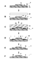
- the manufacturing method of the mold 1 of this embodiment is an inkjet apparatus including a transfer substrate 5 (A in FIG. 3) having a mesa structure including a mesa portion 5a and a flange portion 5b and an inkjet head 40. (Not shown) and by using an inkjet method, a plurality of droplets 41 made of curable resin are arranged on the mesa portion 5a, and a plurality of droplets 42 made of the same curable resin are placed on the flange portion 5b.
- the plurality of droplets 42 disposed on the flange portion 5b are arranged such that the height of each of the plurality of droplets 42 is lower than the height of the mesa portion 5a and the plurality of droplets 42 disposed on the flange portion 5b display the auxiliary mark 30.
- the curable resin and the flange on the mesa portion 5a in a state where the concave / convex pattern 43a of the master mold 43 is pressed against the plurality of droplets 41 arranged on the mesa portion 5a.
- the curable resin on 5b is cured (C in FIG.
- the curable resin 44 on the mesa 5a is removed and the curable resin 45 on the flange 5b is removed using the cured curable resins 44 and 45 as a mask.
- the transferred substrate 5 is etched by the etching gas 46 so that the remaining state remains (D and E in FIG. 3). After this etching is completed, for example, a mold 1 (that is, a double plate of the master mold 43) as shown in E of FIG. 3 can be obtained.
- the visibility of the auxiliary mark 30 is exhibited mainly by the curable resin 45 remaining on the flange portion 5b.
- the transferred substrate 5 is a substrate that is the basis of the mold 1.
- a mesa structure having a mesa portion 5 a and a flange portion 5 b is formed in advance on the transfer substrate 5.
- the master mold 43 C in FIG. 3
- only the droplets 41 disposed on the mesa portion 5a of the transfer substrate 5 are in contact with the master mold 43 and disposed on the flange portion 5b. Contact between the formed droplet 42 and the master mold 43 is avoided.
- the step h of the mesa portion 5a is preferably 1 to 1000 ⁇ m, more preferably 10 to 500 ⁇ m, and still more preferably 20 to 100 ⁇ m. This is because, when the level difference h is lower than the height of the droplet 42 arranged on the flange portion 5b (considering a general droplet amount, it is about 500 nm to several ⁇ m), the droplet 42 and the master This is because the mold 43 may come into contact and contaminate the master mold 43. On the other hand, when the level difference h is too high, the distance between the droplet discharge port of the inkjet head 40 and the flange portion upper surface 5d is increased, so that the droplet placement accuracy is deteriorated.
- the shape of the substrate 5 to be transferred is, for example, a disk shape when the use of the mold 1 is manufacture of an information recording medium.
- the transfer substrate 5 is used to enable exposure to the curable resin.
- a quartz substrate is preferred.
- the quartz substrate is appropriately selected according to the purpose without particular limitation as long as it has light transparency and a thickness of 0.3 mm or more.
- a quartz substrate surface covered with an adhesion layer such as a silane coupling agent, or a metal film made of Cr, W, Ti, Ni, Ag, Pt, Au or the like is laminated on the quartz substrate.
- the transfer substrate 5 does not have a metal-containing film such as the above metal film or metal oxide film will be described.
- the adhesion layer is not essential, but is appropriately used for improving the adhesion between the curable resin and the transfer substrate 5.
- the adhesion layer should just be formed in the pattern formation area (area
- the above-mentioned “having light transparency” specifically means curing when light is incident from the other surface of the substrate so as to be emitted from one surface on which the curable resin film is formed. This means that the functional resin is sufficiently cured, and at least the transmittance of light having a wavelength of 200 nm or more from the other surface to the one surface is 5% or more.
- the thickness of the quartz substrate is usually preferably 0.3 mm or more. This is because if it is 0.3 mm or less, it is likely to be damaged by pressing during handling or imprinting.
- the structure and material of the substrate to be transferred 5 are not particularly limited and can be appropriately selected according to the purpose.
- the structure of the transfer substrate 5 may be a single layer structure or a laminated structure as long as it is a mesa structure.
- the material can be appropriately selected from those known as substrate materials, and examples thereof include silicon, nickel, aluminum, glass, and resin. These board
- substrate materials may be used individually by 1 type, and may use 2 or more types together.
- the transferred substrate 5 may be appropriately synthesized or a commercially available product may be used. Moreover, what coat
- the thickness of the transfer substrate 5 (the total thickness of the mesa portion) is not particularly limited and may be appropriately selected depending on the intended purpose, but is preferably 0.05 mm or more, more preferably 0.1 mm or more. . If the thickness of the substrate is less than 0.05 mm, the substrate may be bent during imprinting, and a uniform contact state may not be ensured.
- the curable resin is not particularly limited, but in this embodiment, for example, it is prepared by adding a photopolymerization initiator (about 2% by mass) and a fluorine monomer (0.1 to 1% by mass) to a polymerizable compound. Materials can be used.
- an antioxidant (about 1% by mass) can be added as necessary.
- the material prepared by the above procedure can be cured by, for example, ultraviolet light having a wavelength of 360 nm.
- ultraviolet light having a wavelength of 360 nm.
- Examples of the polymerizable compound include benzyl acrylate (Biscoat (registered trademark) # 160: manufactured by Osaka Organic Chemical Co., Ltd.), ethyl carbitol acrylate (Biscoat (registered trademark) # 190: manufactured by Osaka Organic Chemical Co., Ltd.), polypropylene glycol di In addition to acrylate (Aronix (registered trademark) M-220: manufactured by Toagosei Co., Ltd.), trimethylolpropane PO-modified triacrylate (Aronix (registered trademark) M-310: manufactured by Toagosei Co., Ltd.), etc. The compound A etc. which are represented can be mentioned. Structural formula 1:
- the polymerization initiator may be 2- (dimethylamino) -2-[(4-methylphenyl) methyl] -1- [4- (4-morpholinyl) phenyl] -1-butanone (IRGACURE®). 379: manufactured by Toyotsu Chemiplus Co., Ltd.) and the like.
- the viscosity of the curable resin is 8 to 20 cP, and the surface energy of the curable resin is 25 to 35 mN / m.
- the viscosity of the curable resin is a value measured at 25 ⁇ 0.2 ° C. using a RE-80L rotational viscometer (manufactured by Toki Sangyo Co., Ltd.).
- the rotation speed at the time of measurement was 100 rpm when 0.5 cP or more and less than 5 cP, 50 rpm when 5 cP or more and less than 10 cP, 20 rpm when 10 cP or more and less than 30 cP, and 10 rpm when 30 cP or more and less than 60 cP.
- the surface energy of the curable resin is “UV“ nanoimprint materials: Surface energies, residual layers, and imprint quality ”, H. Schmitt et al., J. Vac. Sci. Technol. B, Vol. 25, Issue 3, The method described in pp. 785-790, 2007. was used. Specifically, the surface energy of a silicon substrate that has been subjected to UV ozone treatment and a silicon substrate that has been surface-treated with Optool (registered trademark) DSX (manufactured by Daikin Corporation) is obtained, and the contact angle of the curable resin to both substrates is determined. The surface energy of the curable resin was calculated.
- the curable resin disposed on the mesa portion 5a and the curable resin disposed on the flange portion 5b may be the same material or different materials.
- a droplet discharge method that can arrange a predetermined amount of droplets at a predetermined position on the transfer substrate 5 such as an inkjet method or a dispense method is used.
- an ink jet printer or a dispenser may be properly used according to a desired droplet amount (amount per droplet disposed).
- a desired droplet amount amount per droplet disposed.
- an ink jet printer is used when the droplet amount is less than 100 nl
- a dispenser is used when the droplet amount is 100 nl or more.
- an ink jet method is used.
- Examples of the inkjet head 40 that discharges droplets from a nozzle include a piezo method, a thermal method, and an electrostatic method. Among these, a piezo method capable of adjusting an appropriate amount of liquid and a discharge speed is preferable. Before arranging the droplets on the substrate 5, the droplet amount and the discharge speed are adjusted in advance. For example, the appropriate amount of liquid is increased at a position on the substrate 5 corresponding to a region where the spatial volume of the concave / convex pattern of the master mold 43 is large, or on the substrate 5 corresponding to a region where the spatial volume of the concave / convex pattern of the master mold 43 is small. It is preferable to adjust the position by decreasing the number.
- Such adjustment is appropriately controlled according to the discharge amount of the droplets (the amount per droplet when discharged). For example, when an ink jet head having an ejection amount of 1 pl is used and the droplet amount is set to 5 pl, the droplet amount is controlled by ejecting it to the same place five times.
- the amount of droplets is obtained, for example, by measuring the three-dimensional shape of the droplets discharged on the substrate 5 (or another substrate of the same quality) in advance under the same conditions with a confocal microscope and calculating the volume from the shape. It is done.
- the droplets are arranged on the transfer substrate 5 according to a predetermined droplet arrangement pattern.
- the droplet arrangement pattern is configured by two-dimensional coordinate information including a lattice point group corresponding to the droplet arrangement. This droplet arrangement pattern is designed based on the imprint conditions and the shape and size of the auxiliary mark.
- the arrangement of the droplets 42 on the flange portion 5b is such that the height of each of the plurality of droplets 42 arranged on the flange portion 5b is lower than the height of the mesa portion 5a and the plurality of droplets 42 arranged on the flange portion 5b.
- the droplet 42 is displayed so as to display the auxiliary mark. Since the height of each of the plurality of droplets 42 is lower than the height of the mesa portion 5a, the droplets 42 can be prevented from adhering to the master mold 43 during imprinting by the master mold 43.
- the master mold 43 also has a mesa structure, it is considered that the possibility that the droplets 42 adhere to the master mold 43 is reduced.
- the height of each of the plurality of droplets 42 is preferably lower than the height of the mesa portion 5a as in the present invention.
- the auxiliary mark 30 can be flexibly changed by changing the arrangement of the droplets.
- the auxiliary mark may be displayed by a line in which a plurality of droplets are combined, or may be displayed by an arrangement of droplets (dots).
- the shape of the auxiliary mark displayed by the droplet may not necessarily match the final shape of the auxiliary mark 30. That is, the final line of the auxiliary mark 30 becomes thinner or the dot becomes smaller. Therefore, when displaying the auxiliary mark with the droplet, in consideration of the above, for example, the amount of the droplet is increased or the line is thickened so that the information transmission function of the auxiliary mark 30 is not impaired by the etching process. There is a need to.
- the droplet placement on the mesa portion 5a and the droplet placement on the flange portion 5b may be performed simultaneously or separately.
- performing these droplet arrangements “simultaneously” means that the droplet arrangement on the mesa 5a and the droplet arrangement on the flange 5b within a one-way scan of a droplet discharge unit such as an inkjet head.
- “separately” performing these droplet arrangements means that only the droplet arrangement on the mesa unit 5a and the scanning to the flange unit 5b are performed in the scanning movement of the droplet discharge unit. This means that the scanning that only performs droplet placement is completely separated.
- each of these droplet arrangements can be performed using different ink jet heads.
- the contact area between the droplet 42 per droplet disposed on the flange portion 5b and the flange portion 5b that is, the upper surface 5d of the flange portion 5b.
- the contact area between the droplet 41 and the mesa portion 5a arranged on the mesa portion 5a that is, the mesa portion.
- the plurality of droplets are preferably arranged so as to be larger than the average area of the area of the upper surface 5c of 5a in contact with one droplet 41). This is due to the following reason.
- the droplet arrangement on the mesa portion 5a and the droplet arrangement on the flange portion 5b are the same except for the droplet arrangement pattern (for example, the material of the droplet). , Discharge amount, droplet amount, surface energy, etc.).
- the droplets on the flange portion 5b are used.
- the arrangement condition necessarily depends on the condition of the droplet arrangement on the mesa portion 5a.
- the contact area of the droplet 42 on the flange portion 5 b is made larger than the contact area of the droplet 41 on the mesa portion 5 a.
- the contact area of a droplet per droplet means a contact area in a state where the droplet is in a single state (that is, a state where it is not combined with other droplets). Therefore, when the shape of the auxiliary mark is displayed with a line in which a plurality of droplets are combined, the above contact area means the contact area when the above single state is assumed, and this can be confirmed by a prior test. It is. Further, when a plurality of droplets are ejected to the same place, the whole is considered as one droplet.
- the droplet amount per droplet disposed on the flange portion 5b is set to the droplet disposed on the mesa portion 5a.
- a method of increasing the amount of droplets per droplet can be mentioned.
- the method for adjusting the droplet amount is as described above.
- the contact area of the droplet 42 can be increased.
- the contact area is expanded due to the effect of wetting and spreading even with the same droplet amount.
- the wettability of the flange portion 5b is increased by a surface treatment method such as performing UV ozone treatment only on the flange portion 5b or forming a thin film (for example, an organic molecular film) having high affinity with the curable resin. can do.
- the width of the contact surface between the droplet 42 and the flange portion 5b for each droplet is 50 to 500 ⁇ m. It is preferable to arrange the droplets 42 on the flange portion 5b.
- the droplet height can also be controlled by changing the wettability (surface energy) of the transfer substrate 5 and the droplet amount. For example, when the surface energy of the mesa portion upper surface 5c is increased, the wettability is improved and the droplet height is decreased.
- the surface energy of the mesa portion upper surface 5c is increased, the wettability is improved and the droplet height is decreased.
- a thin film for example, an organic molecular film having a high affinity with the curable resin is formed only on the surface of the mesa portion 5a. There are ways to film.
- the height of the droplet 42 can also be increased by increasing the amount of the droplet 42 disposed on the flange portion 5b.
- the surface protective tape is not particularly limited as long as it is a commercially available protective tape for semiconductor wafers. Since there is a concern of adhesive residue when the surface protection tape is peeled off, a method of attaching the surface protection tape to the flange portion 5b is more preferable than on the mesa portion 5a to be imprinted.
- the surface that is not protected by means such as UV ozone cleaning, spin coating, dip coating, spray coating, or vapor deposition is surface treated. After the surface treatment, the surface protective tape is peeled off, so that different surface treatments are performed on the mesa portion 5a and the flange portion 5b.
- the master mold 43 used in the present embodiment can be manufactured by the following procedure, for example. First, on a silicon substrate, a PHS (polyhydroxystyrene) -based chemically amplified resist, a novolac-based resist, a resist solution mainly composed of an acrylic resin such as PMMA (polymethylmethacrylate), or the like is applied by spin coating or the like. Form a layer. Thereafter, the silicon substrate is irradiated with laser light (or electron beam) while being modulated corresponding to the desired concavo-convex pattern, and the concavo-convex pattern is exposed on the surface of the resist layer. Thereafter, the resist layer is developed, and selective etching is performed by RIE (reactive ion etching) using the removed resist layer pattern as a mask to obtain a silicon mold having a predetermined uneven pattern.
- RIE reactive ion etching
- the master mold 43 is not limited to this, and a quartz mold can also be used.
- the quartz mold can be manufactured by a method similar to the manufacturing method of the silicon mold, a replication method of the silicon mold, or the like.
- the master mold 43 may also have a mesa structure.
- the shape of the concavo-convex pattern 43a of the master mold 43 is not particularly limited, and is appropriately selected according to the use of nanoimprint.
- a typical pattern is a line & space pattern.
- interval of convex parts, and the height (the depth of a recessed part) of a convex part from a recessed part bottom face are set suitably.
- the width of the protrusions is 10 to 100 nm, more preferably 20 to 70 nm
- the distance between the protrusions is 10 to 500 nm, more preferably 20 to 100 nm
- the height of the protrusions is 10 to 500 nm.
- the thickness is preferably 30 to 100 nm.
- corrugated pattern 43a may be the shape where the dot which has cross sections, such as a rectangle, a circle
- release agent In the present invention, it is preferable to perform a release treatment on the surface of the master mold 43 in order to improve the release property between the curable resin and the master mold 43.
- the mold release agent used for the mold release treatment Opkin (registered trademark) DSX manufactured by Daikin Industries, Ltd., Novec (registered trademark) EGC-1720 manufactured by Sumitomo 3M Co., Ltd., and the like are used as fluorine-based silane coupling agents. .
- fluorine resins hydrocarbon lubricants, fluorine lubricants, fluorine silane coupling agents and the like can be used.
- PTFA polytetrafluoroethylene
- PFA tetrafluoroethylene / perfluoroalkyl vinyl ether copolymer
- FEP tetrafluoroethylene / hexafluoropropylene copolymer
- ETFE tetrafluoroethylene Ethylene copolymer
- hydrocarbon lubricants include carboxylic acids such as stearic acid and oleic acid, esters such as butyl stearate, sulfonic acids such as octadecyl sulfonic acid, phosphate esters such as monooctadecyl phosphate, stearyl alcohol and oleyl
- carboxylic acids such as stearic acid and oleic acid
- esters such as butyl stearate
- sulfonic acids such as octadecyl sulfonic acid
- phosphate esters such as monooctadecyl phosphate
- alcohols such as alcohol, carboxylic acid amides such as stearamide, and amines such as stearylamine.
- examples of the fluorine-based lubricant include a lubricant in which part or all of the alkyl group of the hydrocarbon-based lubricant is substituted with a fluoroalkyl group or a perfluoropolyether group.
- perfluoropolyether groups include perfluoromethylene oxide polymer, perfluoroethylene oxide polymer, perfluoro-n-propylene oxide polymer (CF 2 CF 2 CF 2 O) n , perfluoroisopropylene oxide polymer ( CF (CF 3 ) CF 2 O) n or a copolymer thereof.
- the subscript n represents the degree of polymerization.
- the fluorine-based silane coupling agent has at least one, preferably 1 to 10 alkoxysilane groups or chlorosilane groups in the molecule, and preferably has a molecular weight of 200 to 10,000.
- the alkoxysilane group includes —Si (OCH 3 ) 3 group and —Si (OCH 2 CH 3 ) 3 group
- the chlorosilane group includes —Si (Cl) 3 group.
- heptadecafluoro-1,1,2,2-tetra-hydrodecyltrimethoxysilane pentafluorophenylpropyldimethylchlorosilane, tridecafluoro-1,1,2,2-tetra-hydrooctyltriethoxy
- compounds such as silane and tridecafluoro-1,1,2,2-tetra-hydrooctyltrimethoxysilane.
- the residual gas is reduced by reducing the atmosphere between the master mold 43 and the substrate 5 to a reduced pressure or vacuum atmosphere.
- the curable resin before curing volatilizes, and it may be difficult to maintain a uniform film thickness. Therefore, the residual gas is preferably reduced by setting the atmosphere between the master mold 43 and the substrate 5 to a He atmosphere or a reduced pressure He atmosphere. Since He permeates the quartz substrate, the trapped residual gas (He) gradually decreases. Since it takes time to permeate He, it is more preferable to use a reduced pressure He atmosphere.
- the reduced pressure atmosphere is preferably 1 to 90 kPa, particularly preferably 1 to 10 kPa.
- the pressing pressure of the master mold 43 is in the range of 100 kPa to 10 MPa.
- the pressure is higher, the flow of the curable resin is promoted, and the compression of the residual gas, the dissolution of the residual gas in the curable resin, and the permeation of He in the quartz substrate are promoted, leading to an improvement in the removal rate.
- the pressing pressure of the master mold 43 is preferably 100 kPa or more and 10 MPa or less, more preferably 100 kPa or more and 5 MPa, and further preferably 100 kPa or more and 1 MPa or less.
- the reason why the pressure is set to 100 kPa or more is that when imprinting is performed in the atmosphere, when the space between the master mold 43 and the substrate 5 is filled with liquid, the pressure between the master mold 43 and the substrate 5 is increased at atmospheric pressure (about 101 kPa). This is because.
- the exposure of the curable resin on the mesa unit 5a is performed in a state where the concave / convex pattern 43a of the master mold 43 is pressed against the droplet 41 arranged on the mesa unit 5a. Thereby, the droplet 41 becomes a curable resin film to which the concave / convex pattern 43a is transferred.
- the curable resin on the flange portion 5b is also cured by exposure to basically the shape when the droplets are arranged. At this time, the exposure of the mesa portion 5a and the flange portion 5b may be performed simultaneously or separately.
- the peeling is performed, for example, by holding the outer edge of either the master mold 43 or the substrate 5 and sucking the back surface of the other substrate 5 or the master mold 43.
- There is a method of peeling by holding the outer edge holding part or the rear surface holding part relative to the direction opposite to the pressing in the held state.
- etching Etching of the transfer substrate 5 is performed using the cured curable resins 44 and 45 as a mask. As a result, a pattern corresponding to the concavo-convex pattern of the master mold 43 is formed on the mesa portion upper surface 5 c of the transferred substrate 5, and the auxiliary mark 30 is formed on the flange portion upper surface 5 d of the transferred substrate 5. Furthermore, in this embodiment, etching is performed so that the curable resin 44 on the mesa portion 5a is removed and the curable resin 45 on the flange portion 5b remains (E in FIG. 3).
- the contrast is improved due to the difference in optical characteristics between the substrate to be transferred and the curable resin, and the visibility of the auxiliary mark 30 is improved.
- the film thickness of the imprinted curable resin 44 (the thickness of the entire protrusion including the so-called remaining film portion) is smaller than 1 ⁇ m. Therefore, if the height of the curable resin 45 is adjusted to be larger than the film thickness of the curable resin 44, the above state can be realized at the timing of the end of etching.
- an appropriate etching time can be obtained in consideration of the film thickness of the curable resin 44 obtained in advance on a trial basis, the height of the curable resin 45, the etching rate of the curable resins 44 and 45, and the like. it can. It is also possible to realize the above state by making the curable resins disposed in the mesa portion 5a and the flange portion 5b different from each other and making a difference in the etching rate.
- Etching is not particularly limited as long as it can form a concavo-convex pattern on the substrate, and can be appropriately selected according to the purpose. Examples thereof include ion milling, reactive ion etching (RIE), and sputter etching. Can be mentioned. Among these, ion milling and RIE are particularly preferable.
- the ion milling method also called ion beam etching, introduces an inert gas such as Ar into the ion source to generate ions. This is accelerated through the grid, and collides with the sample substrate for etching.
- the ion source include a Kaufman type, a high frequency type, an electron impact type, a duoplasmatron type, a Freeman type, an ECR (electron cyclotron resonance) type, and the like.
- Ar gas and fluorine gas or chlorine gas can be used as RIE etchant.
- the curable resin droplets are arranged by the droplet discharge method so as to display the auxiliary marks, and then the curable resin is etched as a mask. Even if it is desired to change the auxiliary mark every time, the auxiliary mark can be easily changed only by changing the design of the arrangement position of the droplets. As a result, in the production of a mesa mold having an auxiliary mark, it is possible to flexibly cope with the change of the auxiliary mark, and it is possible to manufacture more efficiently.
- etching is performed so that the curable resin 44 on the mesa portion 5a is removed and the curable resin 45 on the flange portion 5b remains, but even if all the curable resin is removed. Good.
- the auxiliary mark 30 is displayed by the unevenness of the flange portion itself.
- thermosetting resin for example
- the method of displaying the auxiliary mark with droplets can be applied to a flat substrate to be transferred that does not have a mesa structure if a master mold having a mesa structure is used.
- FIG. 4 is a schematic cross-sectional view showing the steps of the mold manufacturing method according to the present embodiment.
- This embodiment is different from the first embodiment in that only the flange portion 5b of the transfer substrate 5 has the metal-containing film 6 on the surface thereof. Therefore, a detailed description of the same configuration as that of the first embodiment is omitted unless particularly required.
- the manufacturing method of the mold 1 of the present embodiment has a mesa structure including a mesa portion 5a and a flange portion 5b, and the flange portion 5b has a metal-containing film 6 on the surface thereof.
- a plurality of droplets 42 made of the same curable resin are disposed on the flange portion 5b and the height of each of the plurality of droplets 42 disposed on the flange portion 5b is lower than the height of the mesa portion 5a.
- a plurality of droplets 42 are arranged so as to display the auxiliary mark 30 (B in FIG. 4), and the concave / convex pattern 43a of the master mold 43 is pressed against the plurality of droplets 41 arranged on the mesa portion 5a. In this state, the curable resin on the mesa portion 5a and the curable resin on the flange portion 5b are cured (C in FIG.
- the curable resin on the mesa portion 5a is set using the cured curable resins 44 and 45 as a mask.
- Etching of the transfer substrate 5 is performed with an etching gas 46 so that the curable resin 45 on the flange portion 5b remains (44 in FIG. 4D and E), and then on the flange portion 5b.
- the remaining curable resin 45 is removed (F in FIG. 4).
- a mold 1 as shown in FIG. 4F that is, a double plate of the master mold 43
- the visibility of the auxiliary mark 30 is exhibited mainly by the metal-containing film 6 patterned on the flange portion 5b.
- the metal-containing film is a film composed of a material mainly containing a metal such as a metal or a metal compound.
- the “main component” means that the composition ratio in the material is 50% by mass or more.
- the reflectance of the metal-containing film is preferably 30% or more, more preferably 50% or more, and further preferably 70% or more at a wavelength of 365 nm.
- the thickness of the metal-containing film is usually 2 to 30 nm, preferably 5 to 20 nm.
- the metal-containing film can be formed by a film forming method such as a vacuum evaporation method or a sputtering method.
- a film forming method such as a vacuum evaporation method or a sputtering method.
- the material for the metal-containing film include Cr, W, Ti, Ni, Ag, Pt, Au, CrO 2 , WO 2 , and TiO 2 .
- the metal-containing film 6 before etching only needs to constitute at least the surface on which the auxiliary mark 30 is to be formed in the upper surface 5d of the flange portion.
- the identification mark may be formed by combining the pattern formed by a general photolithography technique and the droplet arrangement pattern.
- FIG. 5 is a schematic view showing a manufacturing process in the case where the metal-containing film 6 has a concavo-convex structure finer than the size of a droplet.
- the black portion of the metal-containing film 6 represents a convex portion
- the white portion represents a concave portion.
- the fine uneven structure of the metal-containing film 6 is formed in advance by, for example, a photolithography technique.
- Method for removing curable resin for example, from the state of E in FIG. 4, a wet process such as cleaning in acid or alkali can be adopted, and a dry process such as UV ozone treatment or oxygen ashing is adopted. You can also.
- the mold manufacturing method of the present embodiment also etches using the curable resin as a mask after disposing the curable resin droplets by the droplet discharge method so as to display the auxiliary marks.
- the same effects as those of the first embodiment are obtained.
- the auxiliary mark is displayed by the metal-containing film patterned on the flange portion 5b, the visibility can be improved.
- the metal-containing film has a concavo-convex structure finer than the size of the droplet, an auxiliary mark including a fine pattern exceeding the resolution of the droplet arrangement drawing can be formed.
- FIG. 6 is a schematic cross-sectional view showing the steps of the mold manufacturing method according to the present embodiment.
- This embodiment differs from the second embodiment in that the mesa portion 5a of the transfer substrate 5 also has a metal-containing film 6 on its surface. Therefore, a detailed description of the same configuration as in the first and second embodiments is omitted unless particularly required.
- the manufacturing method of the mold 1 of this embodiment has a mesa structure including a mesa portion 5a and a flange portion 5b, and the mesa portion 5a and the flange portion 5b have a metal-containing film 6 on the surface thereof.
- a plurality of droplets 41 made of a curable resin are arranged on the mesa portion 5a by an ink jet method using the substrate to be transferred 5 (A in FIG. 6) and an ink jet apparatus (not shown) including the ink jet head 40.
- the plurality of liquid droplets 42 made of the same curable resin on the flange portion 5b, the height of each of the plurality of liquid droplets 42 arranged on the flange portion 5b is lower than the height of the mesa portion 5a, and on the flange portion 5b.
- the plurality of droplets 42 arranged on the surface of the master mold 43 are arranged so as to display auxiliary marks (B in FIG. 6), and the concave / convex pattern 4 of the master mold 43 is arranged on the plurality of droplets 41 arranged on the mesa portion 5a.
- the curable resin on the mesa portion 5a and the curable resin on the flange portion 5b are cured in a state where a is pressed (C in FIG.
- the transferred substrate 5 is etched by the etching gas 46 so that the metal-containing film 6 of the mesa 5a is removed and the metal-containing film 6 of the flange 5b remains (from D in FIG. 6). F). Thereafter, for example, a mold 1 (that is, a double plate of the master mold 43) as shown in FIG. 6F can be obtained.
- a mold 1 that is, a double plate of the master mold 43
- the visibility of the auxiliary mark 30 is exhibited mainly by the metal-containing film 6 patterned on the flange portion 5b, as in the second embodiment.
- the etching of this embodiment is performed by the following two-stage etching, for example.
- the first etching is performed under conditions suitable for etching the metal-containing film 6 using the curable resin 44 as a mask, and the next etching is performed by etching the transferred substrate 5 using the processed metal-containing film 6 as a mask. Etching under conditions suitable for this. Then, if necessary, the curable resin is also removed. Such etching enables pattern transfer with higher accuracy.
- a resist solution containing a PHS (polyhydroxy styrene) -based chemically amplified resist as a main component was applied by spin coating to form a resist layer.
- a resist layer was developed, the exposed portion was removed, and selective etching was performed by RIE so that the groove depth became 100 nm using the pattern of the removed resist layer as a mask to obtain a Si mold.
- the mold surface was subjected to mold release treatment with OPTOOL DSX by a dip coating method.
- the concavo-convex pattern was formed in a 10 mm square region at the center of the Si substrate.
- the concavo-convex pattern is a line and space pattern having a length of 10 mm, a width of 50 nm, a pitch of 100 nm, and a depth of 100 nm.
- a quartz substrate having a 152 mm square and a thickness of 6.35 mm was used as the substrate.
- a 10 mm square mesa portion having a height of 30 ⁇ m was formed by wet etching in the transferred region at the center of the substrate.
- the surface of the quartz substrate was subjected to surface treatment with KBM-5103 (manufactured by Shin-Etsu Chemical Co., Ltd.), which is a silane coupling agent having excellent adhesion to the resist.
- KBM-5103 was diluted to 1% by mass with PGMEA (propylene glycol monomethyl ether acetate) and applied to the substrate surface by spin coating.
- the coated substrate was annealed on a hot plate at 150 ° C. for 5 minutes to bond the silane coupling agent to the substrate surface.
- Metal-containing thin film A 30 nm thick Cr film was formed on the flange portion by sputtering to form a metal-containing thin film.
- a concavo-convex structure having a square lattice pattern in which dots of 1 ⁇ m square are arranged at a pitch of 2 ⁇ m was formed on the Cr film by using a general photolithography technique.
- a piezo-type inkjet printer, DMP-2838 manufactured by FUJIFILM Dimatix was used.
- DMC-11610 a dedicated 10 pl head, was used for the inkjet head.
- the discharge conditions were adjusted in advance so that the droplet amount was 10 pl.
- the droplet arrangement pattern was a staggered lattice with a droplet interval of 400 ⁇ m, and the droplets were arranged on the entire transfer region on the mesa in accordance with this droplet arrangement pattern. Further, the characters shown in FIG. 2 are drawn on the flange portion by dot arrangement.
- the space between the master mold and the quartz substrate was replaced with 99% by volume or more of He gas, and the pressure was reduced to 20 kPa or less after the He replacement.
- the master mold was brought into contact with droplets made of resist under reduced pressure He conditions.
- pressurization was performed for 5 seconds with a pressing pressure of 1 MPa, and exposure was performed with ultraviolet light including a wavelength of 360 nm so that an irradiation amount became 300 mJ / cm 2 , thereby curing the resist.
- the outer edge part of the quartz substrate and the master mold was mechanically held, and the master mold was peeled from the resist by moving the quartz substrate or the master mold in a direction opposite to the pressing direction.
Landscapes
- Physics & Mathematics (AREA)
- General Physics & Mathematics (AREA)
- Engineering & Computer Science (AREA)
- Mechanical Engineering (AREA)
- Shaping Of Tube Ends By Bending Or Straightening (AREA)
- Moulds For Moulding Plastics Or The Like (AREA)
- Exposure Of Semiconductors, Excluding Electron Or Ion Beam Exposure (AREA)
Description
本発明は、微細な凹凸パターンを表面に有するモールドの製造方法およびそれを利用して製造されたモールドに関するものである。
ナノインプリントは、凹凸パターンを形成した型(一般的にモールド、スタンパ、テンプレートとも呼ばれる)を被転写基板上に塗布されたレジストに押し付け(インプリント)、レジストを力学的に変形または流動させて微細なパターンを精密にレジスト膜に転写する技術である。モールドを一度作製すれば、ナノレベルの微細構造を簡単に繰り返して成型できるため経済的であるとともに、有害な廃棄物および排出物が少ない転写技術であるため、近年、半導体分野等のさまざまな分野への応用が期待されている。
モールドには、メサ部(上面が比較的平らで周囲より高くなっている部分)とその周りのフランジ部を含むメサ構造を有するもの(以下メサ型のモールドともいう)が知られている(例えば特許文献1)。メサ型のモールドを使用してナノインプリントを行った場合には、平坦なモールドを使用した場合に比べ、モールドとレジストとの接触面積が減少して、小さな力でモールドをレジストから剥離できるという利点がある。また、例えば同一の被転写基板に対してパターンを繰り返し転写(ステップ・アンド・リピート)する場合には、メサ型のモールドを使用することで、次のパターンを転写するときにモールドと先に転写されたパターンとが干渉して、先に転写されたパターンが破損することを回避できるという利点もある。
ところで、モールドには、例えば半導体の回路パターンや表面加工用の加工パターン等、転写の対象となる凹凸パターンの他に、アライメントマークや識別マーク等の補助マークが設けられることがある。
従来、このような補助マークを有するモールドの製造方法としては、例えば特許文献2から4の方法が知られている。特許文献2には、レーザ加工機を使用して識別マークをモールドに刻印する方法が開示されている。特許文献3には、微細な凹凸パターンおよび補助マークを有する平坦なマスターモールドと平坦な被転写基板とを使用し、被転写基板へのレジストの塗布、ナノインプリント、およびエッチングの各工程を経て、上記被転写基板に凹凸パターンと同時に補助マークも転写する方法が開示されている。特許文献4には、特許文献3と同様に凹凸パターンと同時に補助マークも平坦な被転写基板に転写した後、凹凸パターンを含む一部の領域をマスクし、補助マークを含むその他の領域をエッチングで後退させる方法が開示されている。
特許文献4の方法によれば、メサ部上に微細な凹凸パターンを有し、フランジ部に補助マークを有するメサ型のモールドを製造することが可能である。
しかしながら、特許文献4の方法では、補助マークがマスターモールドに固定されているため補助マークを容易に変更することができない。これにより、例えば1つのマスターモールドから複数のモールドを複製する場合であっても、複製したモールドごとに識別マークを変更することができない。また、特許文献4の方法では、補助マークを含むその他の領域をエッチングする工程の間、補助マークの形状を完全に維持することが難しく、補助マークとしての機能が害される可能性がある。
一方、補助マークを有するメサ型のモールドの製造方法としては、メサ部上に微細な凹凸パターンを有するメサ型のモールドを製造した後、特許文献2のように、フランジ部に補助マークをレーザ等で刻印する方法も考えられる。しかしながら、このような方法では、モールドごとに刻印しなければならず、製造工程として非効率である。
本発明は上記問題に鑑みてなされたものであり、補助マークを有するメサ型のモールドの製造において、補助マークの変更に柔軟に対応でき、さらにより効率よく製造することを可能とするモールドの製造方法およびそれを利用して製造されたモールドを提供することを目的とするものである。
上記課題を解決するために、本発明に係るモールドの製造方法は、
微細な凹凸パターンと補助マークとを表面に有するモールドの製造方法において、
メサ部およびフランジ部を含むメサ構造を有する被転写基板を使用し、
液滴吐出法により、メサ部上に硬化性樹脂からなる複数の液滴を配置し、フランジ部上に硬化性樹脂からなる複数の液滴を、フランジ部上に配置された複数の液滴のそれぞれの高さがメサ部の高さより低くかつフランジ部上に配置された複数の液滴が補助マークを表示するように配置し、
メサ部上に配置された複数の液滴にマスターモールドの凹凸パターンを押し付けた状態でメサ部上の硬化性樹脂を硬化させ、フランジ部上の硬化性樹脂を硬化させ、
硬化した硬化性樹脂をマスクとして被転写基板のエッチングを行うことを特徴とするものである。
微細な凹凸パターンと補助マークとを表面に有するモールドの製造方法において、
メサ部およびフランジ部を含むメサ構造を有する被転写基板を使用し、
液滴吐出法により、メサ部上に硬化性樹脂からなる複数の液滴を配置し、フランジ部上に硬化性樹脂からなる複数の液滴を、フランジ部上に配置された複数の液滴のそれぞれの高さがメサ部の高さより低くかつフランジ部上に配置された複数の液滴が補助マークを表示するように配置し、
メサ部上に配置された複数の液滴にマスターモールドの凹凸パターンを押し付けた状態でメサ部上の硬化性樹脂を硬化させ、フランジ部上の硬化性樹脂を硬化させ、
硬化した硬化性樹脂をマスクとして被転写基板のエッチングを行うことを特徴とするものである。
そして、本発明に係るモールドの製造方法において、フランジ部上に配置された液滴1つ当たりの液滴とフランジ部との接触面積が、メサ部上に配置された液滴1つ当たりの液滴とメサ部との接触面積よりも大きくなるように、上記複数の液滴の配置を行うことが好ましい。
また、本発明に係るモールドの製造方法において、液滴とフランジ部との接触面の液滴ごとの幅が50~500μmとなるように、フランジ部上への上記複数の液滴の配置を行うことが好ましい。
また、本発明に係るモールドの製造方法において、フランジ部上に配置された液滴1つ当たりの液滴量が、メサ部上に配置された液滴1つ当たりの液滴量よりも多くなるように、上記複数の液滴の配置を行うことが好ましい。
また、本発明に係るモールドの製造方法において、被転写基板として、フランジ部表面の濡れ性がメサ部表面の濡れ性よりも大きい基板を使用することが好ましい。この場合において、フランジ部のみに、紫外線オゾン処理を施す方法または硬化性樹脂と親和性の高い薄膜を形成する方法により、フランジ部の濡れ性を大きくすることが好ましい。
また、本発明に係るモールドの製造方法において、フランジ部上に配置された液滴の高さが、メサ部上に配置された液滴の高さよりも大きくなるように、上記複数の液滴の配置を行うことが好ましい。
また、本発明に係るモールドの製造方法において、メサ部上への上記複数の液滴の配置およびフランジ部上への上記複数の液滴の配置を同時に行うことが好ましい。
また、本発明に係るモールドの製造方法において、メサ部上の硬化性樹脂が除去されかつフランジ部上の硬化性樹脂が残存する状態となるように上記エッチングを行うことが好ましい。この場合には、被転写基板および硬化性樹脂のそれぞれの光学特性の差によって、補助マークに対してコントラストを付けることができる。
或いは、本発明に係るモールドの製造方法において、被転写基板のフランジ部は、フランジ部の表面の少なくとも一部に金属含有膜を有するものであり、フランジ部上への上記複数の液滴の配置を金属含有膜上に行うことが好ましい。この場合には、被転写基板および金属含有膜のそれぞれの光学特性の差によって、補助マークに対してコントラストを付けることができる。そして、この場合において、金属含有膜は微細な凹凸構造を有するものであることが好ましい。さらに、被転写基板のメサ部はメサ部の表面に金属含有膜を有するものであり、エッチングの後に、硬化性樹脂または金属含有膜をマスクとして、メサ部の金属含有膜が除去されかつフランジ部の金属含有膜が残存する状態となるように、被転写基板のエッチングを行うことが好ましい。
本発明に係るモールドは、上記に記載の方法により製造されたことを特徴とするものである。
本発明に係るモールドの製造方法は、特に、補助マークを表示するように液滴吐出法により硬化性樹脂の液滴を配置した後、硬化したこの硬化性樹脂をマスクとしてエッチングするから、モールドごとに補助マークを変更したい場合でも、液滴の配置場所を設計変更するだけで補助マークを容易に変更することができる。この結果、補助マークを有するメサ型のモールドの製造において、補助マークの変更に柔軟に対応でき、さらにより効率よく製造することが可能となる。
以下、本発明の実施形態について図面を用いて説明するが、本発明はこれに限られるものではない。なお、視認しやすくするため、図面中の各構成要素の縮尺等は実際のものとは適宜異ならせてある。
「補助マークを有するメサ型のモールド」
まず、本発明により得られるモールドについて簡単に説明する。図1は、微細な凹凸パターンと補助マークを有するメサ型のモールドの例を示す概略図である。具体的には、図1のAはモールド1の上面図であり、図1のBはモールド1の正面図である。図2は、識別マークの例を示す概略図である。
まず、本発明により得られるモールドについて簡単に説明する。図1は、微細な凹凸パターンと補助マークを有するメサ型のモールドの例を示す概略図である。具体的には、図1のAはモールド1の上面図であり、図1のBはモールド1の正面図である。図2は、識別マークの例を示す概略図である。
本発明の製造方法によれば、例えば図1のようなメサ型モールド1が製造される。モールド1は、メサ部2およびフランジ部3を含むメサ構造を有し、メサ部2の上面2sはフランジ部3の上面3sよりも段差hの分だけ高くなっている(図1のB)。そして、微細な凹凸パターン21はメサ部2の上面2sに、補助マークはフランジ部3の上面3sに形成されている。
補助マークは、アライメントマークや識別マークなど、モールド1を用いたナノインプリントにおいて、転写の対象とならず、補助的な機能を果たすパターンである。アライメントマークは、インプリントの際のモールドの位置調整を補助するためのパターンであり、識別マークは個々のモールドを識別管理するためのパターンである。識別マークは、例えば、文字、図形、記号、画像、バーコード、ビット記録パターン又はこれらの組合せによってモールドの管理情報を表示する。管理情報とは、例えば、モールドの製造番号、管理番号、製造条件(製造日、温度、原盤種類)、仕様(厚さ、平坦度、平行度、凹凸パターン情報、凹凸パターン配置座標)、使用履歴などである。補助マークは、1以上の線によって構成されてもよいし、図2のように複数のドットの配列によって構成されてもよい。なお、補助マークの検出は、目視観察、マイクロスコープ観察、レーザ計測、電子計算機を用いた画像認識処理などにより行うことができる。
補助マークは、フランジ部3の上面3s自体の凹凸形状によって表示されてもよいし、硬化性樹脂や金属など、フランジ部3(またはモールド1)を構成する材料と異なる材料のパターンによって表示されてもよい。このように、フランジ部3(またはモールド1)を構成する材料と異なる材料をフランジ部3の上面3s上にパターニングすることによって、コントラストが向上し、情報の読み取りが容易となる。補助マークの構成単位の大きさ(例えば、一文字、一図形当たりの大きさ)は、特に制限されないが、検出方法に応じて例えばμmスケールからmmスケールまでの範囲で適宜選択される。補助マークの具体的な形成方法については、後述する各実施形態において詳細に説明する。
なお、補助マークが不要になった場合には、その補助マークを除去することが可能である。例えば、補助マークが硬化性樹脂によって表示されている場合には、酸素アッシング、紫外線(UV)オゾン処理洗浄、および酸やアルカリによる洗浄により、補助マークが金属を含む材料のパターンによって表示されている場合には、酸やアルカリによる洗浄により、補助マークを除去することができる。
「第1の実施形態」
モールド1の製造方法およびその方法により製造されるモールドの第1の実施形態について説明する。図3は、第1の実施形態に係るモールドの製造方法の工程を示す概略断面図である。
モールド1の製造方法およびその方法により製造されるモールドの第1の実施形態について説明する。図3は、第1の実施形態に係るモールドの製造方法の工程を示す概略断面図である。
本実施形態のモールド1の製造方法は、図3に示されるように、メサ部5aおよびフランジ部5bを含むメサ構造を有する被転写基板5(図3のA)とインクジェットヘッド40を含むインクジェット装置(図示省略)とを使用し、インクジェット法により、メサ部5a上に硬化性樹脂からなる複数の液滴41を配置し、フランジ部5b上に同じ硬化性樹脂からなる複数の液滴42を、フランジ部5b上に配置された複数の液滴42のそれぞれの高さがメサ部5aの高さより低くかつフランジ部5b上に配置された複数の液滴42が補助マーク30を表示するように配置し(図3のB)、メサ部5a上に配置された複数の液滴41にマスターモールド43の凹凸パターン43aを押し付けた状態でメサ部5a上の硬化性樹脂およびフランジ部5b上の硬化性樹脂を硬化させ(図3のC)、硬化した硬化性樹脂44および45をマスクとして、メサ部5a上の硬化性樹脂44が除去されかつフランジ部5b上の硬化性樹脂45が残存する状態となるように、エッチングガス46によって被転写基板5のエッチングを行う(図3のDおよびE)ものである。このエッチングの終了後、例えば図3のEに示されるようなモールド1(つまり、マスターモールド43の複盤)を得ることができる。本実施形態では、補助マーク30の視認性は、主にフランジ部5b上に残存する硬化性樹脂45によって発揮されることになる。
(被転写基板)
被転写基板5は、モールド1の基となる基板である。本発明では、メサ型のモールド1を製造するため、被転写基板5には、メサ部5aおよびフランジ部5bを有するメサ構造が予め形成されている。このメサ構造により、マスターモールド43によるインプリント時(図3のC)には、被転写基板5のメサ部5aに配置された液滴41のみがマスターモールド43と接触し、フランジ部5bに配置された液滴42とマスターモールド43との接触は回避される。メサ部5aの段差hは、好ましくは1~1000μm、より好ましくは10~500μm、さらに好ましくは20~100μmである。これは、段差hがフランジ部5bに配置された液滴42の高さ(一般的な液滴量を考慮すると、およそ500nm~数μmである)より低い場合には、この液滴42とマスターモールド43が接触しマスターモールド43を汚染する可能性があるためである。一方、段差hが高すぎる場合には、インクジェットヘッド40の液滴吐出口とフランジ部上面5dとの距離が離れるため、液滴配置精度が悪くなるためである。被転写基板5の形状は、例えば、モールド1の用途が情報記録媒体の製造である場合には、円板状である。
被転写基板5は、モールド1の基となる基板である。本発明では、メサ型のモールド1を製造するため、被転写基板5には、メサ部5aおよびフランジ部5bを有するメサ構造が予め形成されている。このメサ構造により、マスターモールド43によるインプリント時(図3のC)には、被転写基板5のメサ部5aに配置された液滴41のみがマスターモールド43と接触し、フランジ部5bに配置された液滴42とマスターモールド43との接触は回避される。メサ部5aの段差hは、好ましくは1~1000μm、より好ましくは10~500μm、さらに好ましくは20~100μmである。これは、段差hがフランジ部5bに配置された液滴42の高さ(一般的な液滴量を考慮すると、およそ500nm~数μmである)より低い場合には、この液滴42とマスターモールド43が接触しマスターモールド43を汚染する可能性があるためである。一方、段差hが高すぎる場合には、インクジェットヘッド40の液滴吐出口とフランジ部上面5dとの距離が離れるため、液滴配置精度が悪くなるためである。被転写基板5の形状は、例えば、モールド1の用途が情報記録媒体の製造である場合には、円板状である。
硬化性樹脂が光硬化性のものであり、かつ、マスターモールドがシリコン(Si)など光透過性を有さない場合には、硬化性樹脂への露光を可能とするために被転写基板5は石英基板であることが好ましい。石英基板は、光透過性を有し、厚みが0.3mm以上であれば、特に制限されることなく、目的に応じて適宜選択される。例えば被転写基板5としては、石英基板表面をシランカップリング剤などの密着層で被覆したものや、石英基板上にCr、W、Ti、Ni、Ag、Pt、Auなどからなる金属膜を積層したものや、石英基板上にCrO2、WO2、TiO2などからなる金属酸化膜を積層したものや、前記積層体の表面をシランカップリング剤などの密着層で被覆したもの、などが挙げられる。なお、本実施形態では、被転写基板5が上記の金属膜や金属酸化膜などの金属含有膜を有さない場合について説明する。被転写基板5が金属含有膜を有する場合については第2および第3の実施形態で説明する。密着層は、必須ではないが、硬化性樹脂と被転写基板5の密着性を向上させるために適宜使用する。密着層は、少なくともメサ部5aのパターン形成領域(凹凸パターンを形成する領域)に形成されていれば良い。
また、上記「光透過性を有する」とは、具体的には、硬化性樹脂の膜が形成される一方の面から出射するように、基板の他方の面から光を入射した場合に、硬化性樹脂が十分に硬化することを意味しており、少なくとも、上記他方の面から上記一方の面へ波長200nm以上の光の透過率が5%以上であることを意味する。
石英基板の厚みは、通常0.3mm以上が好ましい。0.3mm以下では、ハンドリングやインプリント中の押圧で破損しやすいためである。
一方、マスターモールド43が石英など光透過性を有する場合には、被転写基板5の構造、材料については特に制限はなく、目的に応じて適宜選択することができる。被転写基板5において構造としては、メサ構造であれば、単層構造であってもよいし、積層構造であってもよい。材料としては、基板材料として公知のものの中から、適宜選択することができ、例えば、シリコン、ニッケル、アルミニウム、ガラス、樹脂、などが挙げられる。これらの基板材料は、1種単独で使用してもよいし、2種以上を併用してもよい。被転写基板5は、適宜合成したものであってもよいし、市販品を使用してもよい。また、表面をシランカップリング剤で被覆したものでも良い。
被転写基板5の厚さ(メサ部における全体の厚さ)としては、特に制限はなく、目的に応じて適宜選択することができるが、0.05mm以上が好ましく、0.1mm以上がより好ましい。基板の厚みが0.05mm未満であると、インプリント時に基板側に撓みが発生し、均一な密着状態を確保できない可能性がある。
(硬化性樹脂)
硬化性樹脂は、特に制限されるものではないが、本実施形態では例えば重合性化合物に、光重合開始剤(2質量%程度)、フッ素モノマー(0.1~1質量%)を加えて調製された材料を用いることができる。
硬化性樹脂は、特に制限されるものではないが、本実施形態では例えば重合性化合物に、光重合開始剤(2質量%程度)、フッ素モノマー(0.1~1質量%)を加えて調製された材料を用いることができる。
また、必要に応じて酸化防止剤(1質量%程度)を添加することもできる。上記の手順により作成した材料は例えば波長360nmの紫外光により硬化することができる。溶解性の悪いものについては少量のアセトンまたは酢酸エチルを加えて溶解させた後、溶媒を留去することが好ましい。
上記重合性化合物としては、ベンジルアクリレート(ビスコート(登録商標)#160:大阪有機化学株式会社製)、エチルカルビトールアクリレート(ビスコート(登録商標)#190:大阪有機化学株式会社製)、ポリプロピレングリコールジアクリレート(アロニックス(登録商標)M-220:東亞合成株式会社製)、トリメチロールプロパンPO変性トリアクリレート(アロニックス(登録商標)M-310:東亞合成株式会社製)等の他、下記構造式1で表される化合物A等を挙げることができる。
構造式1:

構造式1:
また、上記重合開始剤としては、2-(ジメチルアミノ)-2-[(4-メチルフェニル)メチル]-1-[4-(4-モルホリニル)フェニル]-1-ブタノン(IRGACURE(登録商標)379:豊通ケミプラス株式会社製)等のアルキルフェノン系光重合開始剤を挙げることができる。
また、上記フッ素モノマーとしては、下記構造式2で表される化合物B等を挙げることができる。
構造式2:
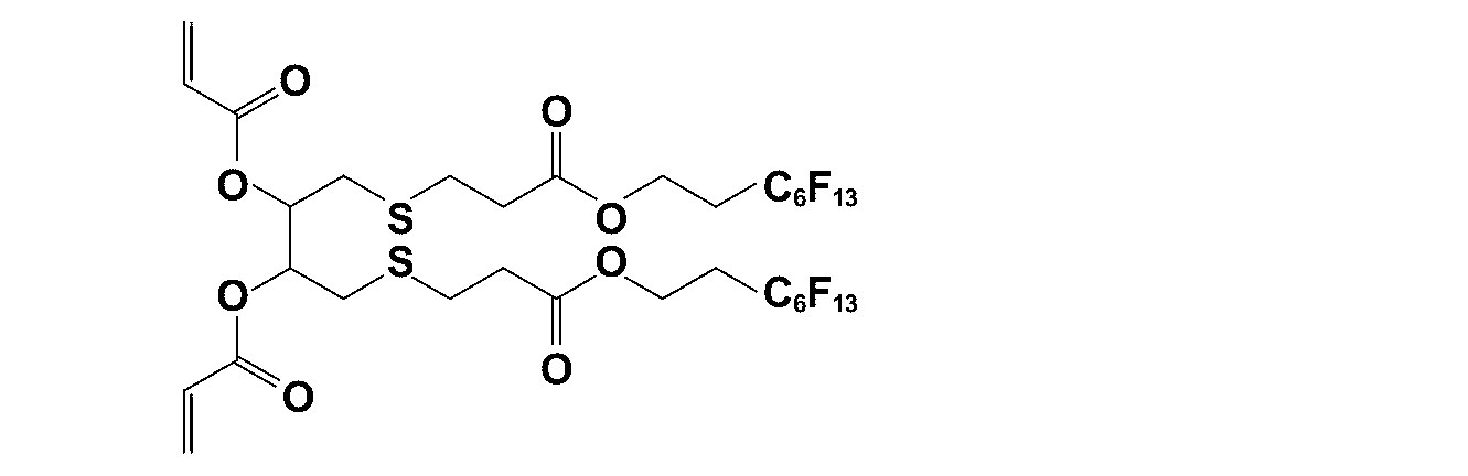
構造式2:
例えば、硬化性樹脂の粘度は8~20cPであり、硬化性樹脂の表面エネルギーは25~35mN/mである。ここで、硬化性樹脂の粘度は、RE-80L型回転粘度計(東機産業株式会社製)を用い、25±0.2℃で測定した値である。測定時の回転速度は、0.5cP以上5cP未満の場合は100rpmとし、5cP以上10cP未満の場合は50rpmとし、10cP以上30cP未満の場合は20rpmとし、30cP以上60cP未満の場合は10rpmとした。また、硬化性樹脂の表面エネルギーは、“UV nanoimprint materials: Surface energies, residual layers, and imprint quality”, H. Schmitt et al., J. Vac. Sci. Technol. B, Vol. 25, Issue 3, pp. 785-790, 2007.に記載の方法を用いた。具体的には、UVオゾン処理をしたシリコン基板と、オプツール(登録商標)DSX(ダイキン株式会社製)により表面処理をしたシリコン基板の表面エネルギーをそれぞれ求め、両基板に対する硬化性樹脂の接触角から硬化性樹脂の表面エネルギーを算出した。
メサ部5a上に配置する硬化性樹脂とフランジ部5b上に配置する硬化性樹脂は、互いに同じ材料であっても異なる材料であってもよい。
(硬化性樹脂からなる液滴の配置方法)
硬化性樹脂からなる液滴の配置方法としてはインクジェット法やディスペンス法など所定の量の液滴を被転写基板5上の所定の位置に配置できる液滴吐出法を用いる。基板5上に液滴を配置する際は、所望の液滴量(配置された液滴1つ当たりの量)に応じてインクジェットプリンターまたはディスペンサーを使い分けても良い。例えば、液滴量が100nl未満の場合はインクジェットプリンターを用い、100nl以上の場合はディスペンサーを用いるなどの方法がある。なお、本実施形態では、インクジェット法を用いるものとする。
硬化性樹脂からなる液滴の配置方法としてはインクジェット法やディスペンス法など所定の量の液滴を被転写基板5上の所定の位置に配置できる液滴吐出法を用いる。基板5上に液滴を配置する際は、所望の液滴量(配置された液滴1つ当たりの量)に応じてインクジェットプリンターまたはディスペンサーを使い分けても良い。例えば、液滴量が100nl未満の場合はインクジェットプリンターを用い、100nl以上の場合はディスペンサーを用いるなどの方法がある。なお、本実施形態では、インクジェット法を用いるものとする。
液滴をノズルから吐出するインクジェットヘッド40には、ピエゾ方式、サーマル方式、静電方式などが挙げられる。これらの中でも、液適量や吐出速度の調整が可能なピエゾ方式が好ましい。基板5上に液滴を配置する前には、あらかじめ液滴量や吐出速度を調整する。例えば、液適量は、マスターモールド43の凹凸パターンの空間体積が大きい領域に対応する基板5上の位置では多くしたり、マスターモールド43の凹凸パターンの空間体積が小さい領域に対応する基板5上の位置では少なくしたりして調整することが好ましい。このような調整は、液滴の吐出量(吐出されたときの液滴1つ当たりの量)に応じて適宜制御される。例えば、吐出量が1plであるインクジェットヘッドを用いて液滴量を5plと設定する場合には、同じ場所に5回吐出して液滴量を制御する。液滴量は、例えば事前に同条件で基板5(或いは同質の他の基板)上に吐出した液滴の3次元形状を共焦点顕微鏡等により測定し、その形状から体積を計算することで求められる。
上記のようにして液滴量を調整した後、所定の液滴配置パターンに従って、被転写基板5上に液滴を配置する。液滴配置パターンは、液滴配置に対応する格子点群からなる2次元座標情報により構成される。この液滴配置パターンは、インプリント条件および補助マークの形状や大きさに基づいて設計される。
フランジ部5b上への液滴42の配置は、フランジ部5b上に配置された複数の液滴42のそれぞれの高さがメサ部5aの高さより低くかつフランジ部5b上に配置された複数の液滴42が補助マークを表示するように行う。複数の液滴42のそれぞれの高さがメサ部5aの高さより低いことにより、マスターモールド43によるインプリント時に、液滴42がマスターモールド43に付着することを防止できる。マスターモールド43もメサ構造を有する場合には、液滴42がマスターモールド43に付着する可能性は低減すると考えられる。しかしながら、例えば、位置調整のためにマスターモールド43の平行移動(被転写基板5との距離が一定に保たれた移動)を行う際にそのような液滴の付着の問題が残る。したがって、マスターモールド43の形状に関わらず、本発明のように複数の液滴42のそれぞれの高さはメサ部5aの高さより低いことが好ましい。また、本発明では、複数の液滴42によって補助マーク30の形状を表示するから、液滴の配置を変更することで柔軟に補助マーク30を変更することが可能となる。
前述したように、補助マークは、複数の液滴が結合した線で表示してもよいし、液滴(ドット)の配列によって表示してもよい。なお、実際には、エッチング工程を経るため、液滴によって表示した補助マークの形状と最終的な補助マーク30の形状とは必ずしも一致しない場合もある。つまり、最終的な補助マーク30の線が細くなったりドットが小さくなったりする。したがって、液滴によって補助マークを表示する際には、上記のことを考慮して、エッチング工程によって補助マーク30の情報伝達機能が害されないように、例えば液滴量を増やしたり線を太くしたりする必要がある。
メサ部5a上への液滴配置とフランジ部5bへの液滴配置とは、同時に行っても良いし、別々に行ってもよい。ここで、これらの液滴配置を「同時に」行うとは、インクジェットヘッド等の液滴吐出部の片道走査内に、メサ部5a上への液滴配置とフランジ部5b上への液滴配置とが行われることを意味し、これらの液滴配置を「別々に」行うとは、液滴吐出部の走査移動において、メサ部5a上への液滴配置のみを行う走査とフランジ部5bへの液滴配置のみを行う走査とが完全に分かれていることを意味する。さらには、これらの液滴配置のそれぞれを相互に異なるインクジェットヘッドを使用して行うことも可能である。しかしながら、メサ部5aおよびフランジ部5bそれぞれへの液滴配置に関して、別々の硬化性樹脂および別々のインクジェットヘッドを使用すると、液滴配置に要する時間が増加するため、同じ硬化性樹脂および同じインクジェットヘッドを使用して同時に液滴配置することが最も好ましい。
本発明では、補助マーク30の視認性を向上させる観点から、フランジ部5b上に配置された液滴1つ当たりの液滴42とフランジ部5bとの接触面積(つまり、フランジ部5bの上面5dのうち1つの液滴42が接している領域の面積の平均値)が、メサ部5a上に配置された液滴1つ当たりの液滴41とメサ部5aとの接触面積(つまり、メサ部5aの上面5cのうち1つの液滴41が接している領域の面積の平均値)よりも大きくなるように、上記複数の液滴の配置を行うことが好ましい。これは、以下の理由による。液滴配置の単純な方法としては、メサ部5a上への液滴配置とフランジ部5b上への液滴配置とを、液滴配置パターンを除いて、全く同一条件(例えば、液滴の材料、吐出量、液滴量、表面エネルギーなど)で行う方法が考えられる。ただし、メサ部5a上への液滴配置の条件は、マスターモールド43によるインプリントとの関係で決まることが多いため、そのような方法を実施する場合には、フランジ部5b上への液滴配置の条件がメサ部5a上への液滴配置の条件に必然的に従属することになる。ところで、メサ部5a上への液滴配置では、インプリント時の硬化性樹脂膜の未充填欠陥を防止する観点から、小さい液滴を高密度に配置することが要求される。したがって、フランジ部5b上への液滴配置の条件をメサ部5a上への液滴配置の条件に従属させると、線が細い補助マークしか表示できないという問題が生じる可能性がある。これは、完成体のモールド1の補助マーク30の視認性に大きく影響する。そこで、補助マーク30の視認性を向上させる観点から、1つの目安として、フランジ部5b上における液滴42の接触面積をメサ部5a上における液滴41の接触面積よりも大きくするのである。
なお、液滴1つ当たりの液滴の接触面積とは、当該液滴が単独の状態(つまり、他の液滴と結合していない状態)における接触面積を意味する。したがって、複数の液滴が結合した線で補助マークの形状を表示する場合には、上記接触面積とは上記単独の状態を想定した場合の接触面積を意味し、これは事前の試験で確認可能である。また、同じ場所に複数回液滴が吐出された場合には、その全体が1つの液滴として考慮される。
このようにフランジ部5b上における液滴42の接触面積を大きくする方法としては、例えば、フランジ部5b上に配置する液滴1つ当たりの液滴量を、メサ部5a上に配置する液滴1つ当たりの液滴量よりも多くする方法が挙げられる。なお、液滴量の調整方法については前述の通りである。或いは、フランジ部5b上の液滴42に対するフランジ部上面5dの濡れ性がメサ部5a上の液滴41に対するメサ部上面5cの濡れ性よりも大きい被転写基板5を使用することによっても、上記のように液滴42の接触面積を大きくすることができる。濡れ性が大きい(つまり、フランジ部上面5dの表面エネルギーが大きい、または液滴の接触角が小さい)方が、同じ液滴量でも濡れ広がりの効果により接触面積が拡大するためである。例えば、フランジ部5bのみに、UVオゾン処理を施す、または、硬化性樹脂と親和性の高い薄膜(例えば有機分子膜)を形成するなどの表面処理方法により、フランジ部5bの上記濡れ性を大きくすることができる。
さらに、補助マークを肉眼で簡易に確認する観点から、液滴ごとの液滴42とフランジ部5bとの接触面の幅(当該接触面を円で近似したときのその直径)が50~500μmとなるように、フランジ部5b上への液滴42の配置を行うことが好ましい。
一方で、フランジ部5b上に配置された液滴42の高さが、メサ部5a上に配置された液滴41の高さよりも大きくなるように、液滴配置を行うことも有効である。液滴高さも被転写基板5の濡れ性(表面エネルギー)や液滴量を変更することで制御できる。例えば、メサ部上面5cの表面エネルギーを高くすると濡れ性が向上し、液滴高さは小さくなる。表面エネルギーを高くするには、メサ部5aの表面のみをUVオゾン処理等で活性化する方法や、硬化性樹脂と親和性の高い薄膜(例えば有機分子膜)をメサ部5aの表面のみに製膜する方法がある。また、フランジ部5b上へ配置する液滴42の液滴量を増やすことによっても、液滴42の高さを高くすることができる。
メサ部5aおよびフランジ部5bで互いに異なる表面処理をする際は、どちらか一方の表面を表面保護テープで保護する方法が好ましい。表面保護テープは市販の半導体ウエハ用保護テープであれば特に制限はない。表面保護テープを剥がした際の糊残りの懸念があるため、インプリントをするメサ部5a上よりも、フランジ部5bに表面保護テープを貼り付けた法がより好ましい。局所的に表面保護テープを貼り付けた状態で、UVオゾンクリーニング法、スピンコート法、ディップコート法、スプレーコート法、蒸着法などの手段により保護されていない部分が表面処理される。表面処理後、表面保護テープを剥がすことにより、メサ部5aおよびフランジ部5bで異なる表面処理がなされた状態になる。
(マスターモールド)
本実施形態で使用するマスターモールド43は、例えば以下の手順により製造することができる。まず、シリコン基材上に、スピンコートなどでPHS(polyhydroxystyrene)系の化学増幅型レジスト、ノボラック系レジスト、PMMA(ポリメチルメタクリレート)等のアクリル樹脂などを主成分とするレジスト液を塗布し、レジスト層を形成する。その後、シリコン基材にレーザ光(又は電子ビーム)を所望の凹凸パターンに対応して変調しながら照射し、レジスト層表面に凹凸パターンを露光する。その後、レジスト層を現像処理し、除去後のレジスト層のパターンをマスクにしてRIE(反応性イオンエッチング)などにより選択エッチングを行い、所定の凹凸パターンを有するシリコンモールドを得る。
本実施形態で使用するマスターモールド43は、例えば以下の手順により製造することができる。まず、シリコン基材上に、スピンコートなどでPHS(polyhydroxystyrene)系の化学増幅型レジスト、ノボラック系レジスト、PMMA(ポリメチルメタクリレート)等のアクリル樹脂などを主成分とするレジスト液を塗布し、レジスト層を形成する。その後、シリコン基材にレーザ光(又は電子ビーム)を所望の凹凸パターンに対応して変調しながら照射し、レジスト層表面に凹凸パターンを露光する。その後、レジスト層を現像処理し、除去後のレジスト層のパターンをマスクにしてRIE(反応性イオンエッチング)などにより選択エッチングを行い、所定の凹凸パターンを有するシリコンモールドを得る。
なお、本実施形態ではシリコンモールドを用いた場合について説明するが、マスターモールド43はこれに限られず、石英モールドを用いることも可能である。この場合、石英モールドは、上記シリコンモールドの製造法と同様の方法や、上記シリコンモールドの複製方法等により製造することができる。なお、マスターモールド43も、メサ構造を有していてもよい。
マスターモールド43の凹凸パターン43aの形状は、特に限定されず、ナノインプリントの用途に応じて適宜選択される。例えば典型的なパターンとしてライン&スペースパターンである。そして、ライン&スペースパターンの凸部の長さ、凸部の幅、凸部同士の間隔および凹部底面からの凸部の高さ(凹部の深さ)は適宜設定される。例えば、凸部の幅は10~100nm、より好ましくは20~70nmであり、凸部同士の間隔は10~500nm、より好ましくは20~100nmであり、凸部の高さは10~500nm、より好ましくは30~100nmである。また、凹凸パターン43aを構成する凸部の形状は、その他、矩形、円および楕円等の断面を有するドットが配列したような形状でもよい。
(離型剤)
本発明では、硬化性樹脂とマスターモールド43との離型性を向上させるためにマスターモールド43の表面に離型処理を行うことが好ましい。離型処理に使用する離型剤としては、フッ素系のシランカップリング剤として、ダイキン工業株式会社製のオプツール(登録商標)DSXや、住友スリーエム株式会社製のNovec(登録商標)EGC-1720等、が挙げられる。
本発明では、硬化性樹脂とマスターモールド43との離型性を向上させるためにマスターモールド43の表面に離型処理を行うことが好ましい。離型処理に使用する離型剤としては、フッ素系のシランカップリング剤として、ダイキン工業株式会社製のオプツール(登録商標)DSXや、住友スリーエム株式会社製のNovec(登録商標)EGC-1720等、が挙げられる。
この他にも、公知のフッ素系樹脂、炭化水素系潤滑剤、フッ素系潤滑剤、フッ素系シランカップリング剤などが使用できる。
例えばフッ素系樹脂としては、PTFA(ポリテトラフルオロエチレン)、PFA(テトラフルオロエチレン・パーフルオロアルキルビニルエーテル共重合体)、FEP(テトラフルオロエチレン・ヘキサフルオロプロピレン共重合体)、ETFE(テトラフルオロエチレン・エチレン共重合体)などが挙げられる。
例えば炭化水素系潤滑剤としては、ステアリン酸およびオレイン酸等のカルボン酸類、ステアリン酸ブチル等のエステル類、オクタデシルスルホン酸等のスルホン酸類、リン酸モノオクタデシル等のリン酸エステル類、ステアリルアルコールおよびオレイルアルコール等のアルコール類、ステアリン酸アミド等のカルボン酸アミド類、ステアリルアミン等のアミン類などが挙げられる。
例えばフッ素系潤滑剤としては、上記炭化水素系潤滑剤のアルキル基の一部または全部をフルオロアルキル基もしくはパーフルオロポリエーテル基で置換した潤滑剤が挙げられる。
例えばパーフルオロポリエーテル基としては、パーフルオロメチレンオキシド重合体、パーフルオロエチレンオキシド重合体、パーフルオロ-n-プロピレンオキシド重合体(CF2CF2CF2O)n、パーフルオロイソプロピレンオキシド重合体(CF(CF3)CF2O)nまたはこれらの共重合体等である。ここで、添え字のnは重合度を表す。
例えばフッ素系シランカップリング剤としては、分子中に少なくとも1個、好ましくは1~10個のアルコキシシラン基、クロロシラン基を有するものであり、分子量200~10,000のものが好ましい。例えば、アルコキシシラン基としては、-Si(OCH3)3基、-Si(OCH2CH3)3基が挙げられ、クロロシラン基としては、-Si(Cl)3基などが挙げられる。具体的には、ヘプタデカフルオロ-1,1,2,2-テトラ-ハイドロデシルトリメトキシシラン、ペンタフルオロフェニルプロピルジメチルクロロシラン、トリデカフルオロ-1,1,2,2-テトラ-ハイドロオクチルトリエトキシシラン、トリデカフルオロ-1,1,2,2-テトラ-ハイドロオクチルトリメトキシシランなどの化合物である。
(インプリント方法)
マスターモールド43と硬化性樹脂を接触する前に、マスターモールド43と基板5間の雰囲気を減圧または真空雰囲気にすることで残留気体を低減する。ただし、高真空雰囲気下では硬化前の硬化性樹脂が揮発し、均一な膜厚を維持することが困難となる可能性がある。そこで、好ましくはマスターモールド43と基板5間の雰囲気を、He雰囲気または減圧He雰囲気にすることで残留気体を低減する。Heは石英基板を透過するため、取り込まれた残留気体(He)は徐々に減少する。Heの透過には時間を要すため減圧He雰囲気とすることがより好ましい。減圧雰囲気は、1~90kPaであることが好ましく、1~10kPaが特に好ましい。
マスターモールド43と硬化性樹脂を接触する前に、マスターモールド43と基板5間の雰囲気を減圧または真空雰囲気にすることで残留気体を低減する。ただし、高真空雰囲気下では硬化前の硬化性樹脂が揮発し、均一な膜厚を維持することが困難となる可能性がある。そこで、好ましくはマスターモールド43と基板5間の雰囲気を、He雰囲気または減圧He雰囲気にすることで残留気体を低減する。Heは石英基板を透過するため、取り込まれた残留気体(He)は徐々に減少する。Heの透過には時間を要すため減圧He雰囲気とすることがより好ましい。減圧雰囲気は、1~90kPaであることが好ましく、1~10kPaが特に好ましい。
マスターモールド43の押し付け圧は、100kPa以上、10MPa以下の範囲で行う。圧力が大きい方が、硬化性樹脂の流動が促進され、また残留気体の圧縮、残留気体の硬化性樹脂への溶解、石英基板中のHeの透過も促進し、除去率向上に繋がる。しかし、加圧力が強すぎるとマスターモールド43接触時に異物を噛みこんだ際にマスターモールド43及び基板5を破損する可能性がある。よって、マスターモールド43の押し付け圧は、100kPa以上、10MPa以下が好ましく、より好ましくは100kPa以上、5MPa、更に好ましくは100kPa以上、1MPa以下となる。100kPa以上としたのは、大気中でインプリントを行う際、マスターモールド43と基板5間が液体で満たされている場合、マスターモールド43と基板5間が大気圧(約101kPa)で加圧されているためである。
メサ部5a上の硬化性樹脂の露光は、メサ部5a上に配置された液滴41にマスターモールド43の凹凸パターン43aを押し付けた状態で行われる。これにより液滴41は凹凸パターン43aが転写された硬化性樹脂膜となる。フランジ部5b上の硬化性樹脂も露光により、基本的には液滴配置されたときの形状で硬化する。この際、メサ部5aおよびフランジ部5bの露光は同時に行ってもよいし別々に行ってもよい。
マスターモールド43を押し付けて硬化性樹脂膜を形成した後、剥離させる方法としては、例えばマスターモールド43または基板5のどちらかの外縁部を保持し、他方の基板5またはマスターモールド43の裏面を吸引保持した状態で、外縁の保持部もしくは裏面の保持部を押圧と反対方向に相対移動させることで剥離させる方法が挙げられる。
(エッチング)
被転写基板5のエッチングは、硬化した硬化性樹脂44および45をマスクとして行われる。これにより、被転写基板5のメサ部上面5cにマスターモールド43の凹凸パターンに対応したパターンが形成され、被転写基板5のフランジ部上面5dには補助マーク30が形成される。さらに、本実施形態では、メサ部5a上の硬化性樹脂44が除去されかつフランジ部5b上の硬化性樹脂45が残存する状態となるように、エッチングが行われる(図3のE)。補助マーク30に硬化性樹脂を残すことにより、被転写基板および硬化性樹脂のそれぞれの光学特性の差によりコントラストが向上し、補助マーク30の視認性が向上するという効果がある。通常、インプリントされた硬化性樹脂44の膜厚(いわゆる残膜部分を含めた凸部全体の厚さ)は1μmより小さい。したがって、硬化性樹脂45の高さを硬化性樹脂44の膜厚よりも大きくなるように調整しておけば、エッチングの終了のタイミングによって上記状態を実現することは可能である。例えば、試験的に事前に得られた硬化性樹脂44の膜厚、硬化性樹脂45の高さ、並びに硬化性樹脂44および45のエッチングレート等を考慮して、適切なエッチング時間を求めることができる。また、メサ部5aおよびフランジ部5bそれぞれに配置する硬化性樹脂を互いに異なる材料として、エッチングレートに違いを出すことによっても上記状態を実現することは可能である。
被転写基板5のエッチングは、硬化した硬化性樹脂44および45をマスクとして行われる。これにより、被転写基板5のメサ部上面5cにマスターモールド43の凹凸パターンに対応したパターンが形成され、被転写基板5のフランジ部上面5dには補助マーク30が形成される。さらに、本実施形態では、メサ部5a上の硬化性樹脂44が除去されかつフランジ部5b上の硬化性樹脂45が残存する状態となるように、エッチングが行われる(図3のE)。補助マーク30に硬化性樹脂を残すことにより、被転写基板および硬化性樹脂のそれぞれの光学特性の差によりコントラストが向上し、補助マーク30の視認性が向上するという効果がある。通常、インプリントされた硬化性樹脂44の膜厚(いわゆる残膜部分を含めた凸部全体の厚さ)は1μmより小さい。したがって、硬化性樹脂45の高さを硬化性樹脂44の膜厚よりも大きくなるように調整しておけば、エッチングの終了のタイミングによって上記状態を実現することは可能である。例えば、試験的に事前に得られた硬化性樹脂44の膜厚、硬化性樹脂45の高さ、並びに硬化性樹脂44および45のエッチングレート等を考慮して、適切なエッチング時間を求めることができる。また、メサ部5aおよびフランジ部5bそれぞれに配置する硬化性樹脂を互いに異なる材料として、エッチングレートに違いを出すことによっても上記状態を実現することは可能である。
エッチングとしては、基板に凹凸パターンを形成できるものであれば特に制限はなく、目的に応じて適宜選択することができ、例えば、イオンミリング法、反応性イオンエッチング(RIE)、スパッタエッチング、などが挙げられる。これらの中でも、イオンミリング法、RIEが特に好ましい。
イオンミリング法は、イオンビームエッチングとも言われ、イオン源にArなどの不活性ガスを導入し、イオンを生成する。これを、グリッドを通して加速させ、試料基板に衝突させてエッチングするものである。イオン源としては、カウフマン型、高周波型、電子衝撃型、デュオプラズマトロン型、フリーマン型、ECR(電子サイクロトロン共鳴)型などが挙げられる。
イオンビームエッチングでのプロセスガスとしては、Arガス、RIEのエッチャントとしては、フッ素系ガスや塩素系ガスを用いることができる。
以上のように、本実施形態のモールドの製造方法は、補助マークを表示するように液滴吐出法により硬化性樹脂の液滴を配置した後、この硬化性樹脂をマスクとしてエッチングするから、モールドごとに補助マークを変更したい場合でも、液滴の配置場所を設計変更するだけで補助マークを容易に変更することができる。この結果、補助マークを有するメサ型のモールドの製造において、補助マークの変更に柔軟に対応でき、さらにより効率よく製造することが可能となる。
<設計変更>
上記実施形態を応用すれば、一度形成した補助マークを除去した場合であっても、再度硬化性樹脂の液滴をフランジ部のみに配置し、硬化性樹脂を硬化させて、補助マーク30を形成することができる。つまり、本発明の製造方法により製造されたモールド1においては、補助マーク30の消去および追加によって情報の更新が可能である。
上記実施形態を応用すれば、一度形成した補助マークを除去した場合であっても、再度硬化性樹脂の液滴をフランジ部のみに配置し、硬化性樹脂を硬化させて、補助マーク30を形成することができる。つまり、本発明の製造方法により製造されたモールド1においては、補助マーク30の消去および追加によって情報の更新が可能である。
上記実施形態では、メサ部5a上の硬化性樹脂44が除去されかつフランジ部5b上の硬化性樹脂45が残存する状態となるようにエッチングを行ったが、硬化性樹脂はすべて除去されてもよい。この場合には、フランジ部自体の凹凸によって補助マーク30が表示される。
上記の実施形態では、硬化性樹脂が光硬化性を有する場合について説明したが、本発明はこれに限られない。つまり本発明では、例えば熱硬化性樹脂を使用することも可能である。
なお、液滴で補助マークを表示する方法は、メサ構造を有するマスターモールドを使用すれば、メサ構造を有していない平坦な被転写基板に適用することも可能である。
「第2の実施形態」
次に、モールドの製造方法の第2の実施形態について説明する。図4は、本実施形態に係るモールドの製造方法の工程を示す概略断面図である。本実施形態は、被転写基板5のフランジ部5bのみがその表面に金属含有膜6を有する点で、第1の実施形態と異なる。したがって、第1の実施形態と同様の構成についての詳細な説明は特に必要のない限り省略する。
次に、モールドの製造方法の第2の実施形態について説明する。図4は、本実施形態に係るモールドの製造方法の工程を示す概略断面図である。本実施形態は、被転写基板5のフランジ部5bのみがその表面に金属含有膜6を有する点で、第1の実施形態と異なる。したがって、第1の実施形態と同様の構成についての詳細な説明は特に必要のない限り省略する。
本実施形態のモールド1の製造方法は、図4に示されるように、メサ部5aおよびフランジ部5bを含むメサ構造を有しかつフランジ部5bがその表面に金属含有膜6を有する被転写基板5(図4のA)とインクジェットヘッド40を含むインクジェット装置(図示省略)とを使用し、インクジェット法により、メサ部5a上に硬化性樹脂からなる複数の液滴41を配置し、フランジ部5b上に同じ硬化性樹脂からなる複数の液滴42を、フランジ部5b上に配置された複数の液滴42のそれぞれの高さがメサ部5aの高さより低くかつフランジ部5b上に配置された複数の液滴42が補助マーク30を表示するように配置し(図4のB)、メサ部5a上に配置された複数の液滴41にマスターモールド43の凹凸パターン43aを押し付けた状態でメサ部5a上の硬化性樹脂およびフランジ部5b上の硬化性樹脂を硬化させ(図4のC)、硬化した硬化性樹脂44および45をマスクとして、メサ部5a上の硬化性樹脂44が除去されかつフランジ部5b上の硬化性樹脂45が残存する状態となるように、エッチングガス46によって被転写基板5のエッチングを行い(図4のDおよびE)、その後フランジ部5b上に残った硬化性樹脂45を除去する(図4のF)ものである。この硬化性樹脂の除去後、例えば図4のFに示されるようなモールド1(つまり、マスターモールド43の複盤)を得ることができる。本実施形態では、補助マーク30の視認性は、主にフランジ部5b上にパターニングされた金属含有膜6によって発揮されることになる。
(金属含有膜)
金属含有膜は、金属や金属化合物など金属を主成分とする材料から構成される膜である。「主成分」とは、材料中の構成比率が50質量%以上であることを意味する。本実施形態のように、金属含有膜6によって補助マーク30を表示することにより、補助マークの視認性が向上する。視認性を向上させる観点から、金属含有膜の反射率は、365nm波長において、好ましくは30%以上、より好ましくは50%以上、さらに好ましくは70%以上である。金属含有膜の厚さは、通常2~30nm、好ましくは5~20nmにする。特に、30nmを超えるとUV透過性が低下し、硬化性樹脂の硬化不良が起こりやすいためである。金属含有膜は、例えば真空蒸着法やスパッタリング法等の成膜法によって形成することができる。金属含有膜の材料としては、Cr、W、Ti、Ni、Ag、Pt、Au、CrO2、WO2、TiO2などが挙げられる。なお、エッチング前の金属含有膜6は、フランジ部上面5dのうち、少なくとも補助マーク30を形成する予定の表面を構成していればよい。
金属含有膜は、金属や金属化合物など金属を主成分とする材料から構成される膜である。「主成分」とは、材料中の構成比率が50質量%以上であることを意味する。本実施形態のように、金属含有膜6によって補助マーク30を表示することにより、補助マークの視認性が向上する。視認性を向上させる観点から、金属含有膜の反射率は、365nm波長において、好ましくは30%以上、より好ましくは50%以上、さらに好ましくは70%以上である。金属含有膜の厚さは、通常2~30nm、好ましくは5~20nmにする。特に、30nmを超えるとUV透過性が低下し、硬化性樹脂の硬化不良が起こりやすいためである。金属含有膜は、例えば真空蒸着法やスパッタリング法等の成膜法によって形成することができる。金属含有膜の材料としては、Cr、W、Ti、Ni、Ag、Pt、Au、CrO2、WO2、TiO2などが挙げられる。なお、エッチング前の金属含有膜6は、フランジ部上面5dのうち、少なくとも補助マーク30を形成する予定の表面を構成していればよい。
また、液滴配置描画の解像度を超える微細なパターンを含む補助マークを形成したい場合は、一般的なフォトリソグラフィ技術により形成したパターンと液滴配置パターンを複合して識別マークを形成しても良い。例えば、図5は、金属含有膜6が液滴の大きさよりも微細な凹凸構造を有する場合の製造工程を示す概略図である。図5のAにおいては、例えば金属含有膜6の黒い部分が凸部を表し、白い部分が凹部を表している。金属含有膜6の微細な凹凸構造は、例えばフォトリソグラフィ技術によって予め形成される。この場合において、被転写基板5のメサ部5a上に液滴41を配置し、フランジ部5b上に液滴42を配置した後(図5のB)、エッチング工程へ移行する。その結果、図5のCに示されるような微細な凹凸構造を有する補助マーク30が形成される。
(硬化性樹脂の除去方法)
硬化性樹脂の除去方法は、例えば図4のEの状態から、酸またはアルカリ中での洗浄等のウェットプロセスを採用することもでき、またUVオゾン処理や酸素アッシング等のドライプロセスを採用することもできる。
硬化性樹脂の除去方法は、例えば図4のEの状態から、酸またはアルカリ中での洗浄等のウェットプロセスを採用することもでき、またUVオゾン処理や酸素アッシング等のドライプロセスを採用することもできる。
以上のように、本実施形態のモールドの製造方法も、補助マークを表示するように液滴吐出法により硬化性樹脂の液滴を配置した後、この硬化性樹脂をマスクとしてエッチングするから、第1の実施形態と同様の効果を奏する。
さらに本実施形態では、補助マークが、フランジ部5b上にパターニングされた金属含有膜によって表示されるため、視認性を向上させることができる。
さらに、金属含有膜が液滴の大きさよりも微細な凹凸構造を有する場合には、液滴配置描画の解像度を超える微細なパターンを含む補助マークを形成することができる。
「第3の実施形態」
次に、モールドの製造方法の第3の実施形態について説明する。図6は、本実施形態に係るモールドの製造方法の工程を示す概略断面図である。本実施形態は、被転写基板5のメサ部5aもその表面に金属含有膜6を有する点で、第2の実施形態と異なる。したがって、第1および第2の実施形態と同様の構成についての詳細な説明は特に必要のない限り省略する。
次に、モールドの製造方法の第3の実施形態について説明する。図6は、本実施形態に係るモールドの製造方法の工程を示す概略断面図である。本実施形態は、被転写基板5のメサ部5aもその表面に金属含有膜6を有する点で、第2の実施形態と異なる。したがって、第1および第2の実施形態と同様の構成についての詳細な説明は特に必要のない限り省略する。
本実施形態のモールド1の製造方法は、図6に示されるように、メサ部5aおよびフランジ部5bを含むメサ構造を有しかつメサ部5aおよびフランジ部5bがその表面に金属含有膜6を有する被転写基板5(図6のA)とインクジェットヘッド40を含むインクジェット装置(図示省略)とを使用し、インクジェット法により、メサ部5a上に硬化性樹脂からなる複数の液滴41を配置し、フランジ部5b上に同じ硬化性樹脂からなる複数の液滴42を、フランジ部5b上に配置された複数の液滴42のそれぞれの高さがメサ部5aの高さより低くかつフランジ部5b上に配置された複数の液滴42が補助マークを表示するように配置し(図6のB)、メサ部5a上に配置された複数の液滴41にマスターモールド43の凹凸パターン43aを押し付けた状態でメサ部5a上の硬化性樹脂およびフランジ部5b上の硬化性樹脂を硬化させ(図6のC)、硬化した硬化性樹脂44および45または金属含有膜6をマスクとして、メサ部5aの金属含有膜6が除去されかつフランジ部5bの金属含有膜6が残存する状態となるように、エッチングガス46によって被転写基板5のエッチングを行うものである(図6のDからF)。この後、例えば図6のFに示されるようなモールド1(つまり、マスターモールド43の複盤)を得ることができる。本実施形態では、補助マーク30の視認性は、第2の実施形態と同様に、主にフランジ部5b上にパターニングされた金属含有膜6によって発揮されることになる。
(エッチング)
本実施形態のエッチングは、例えば次のような2段階のエッチングによって実施される。最初のエッチングは、硬化性樹脂44をマスクとして金属含有膜6をエッチングするのに適した条件のエッチングであり、次のエッチングは、加工された金属含有膜6をマスクとして被転写基板5をエッチングするのに適した条件のエッチングである。そして、必要に応じて、硬化性樹脂の除去も行われる。このようなエッチングにより、より高精度なパターン転写が可能となる。
本実施形態のエッチングは、例えば次のような2段階のエッチングによって実施される。最初のエッチングは、硬化性樹脂44をマスクとして金属含有膜6をエッチングするのに適した条件のエッチングであり、次のエッチングは、加工された金属含有膜6をマスクとして被転写基板5をエッチングするのに適した条件のエッチングである。そして、必要に応じて、硬化性樹脂の除去も行われる。このようなエッチングにより、より高精度なパターン転写が可能となる。
本発明に係るモールドの製造方法の実施例を以下に示す。
(マスターモールドの作製)
Si基材上に、スピンコートによりPHS(polyhydroxy styrene)系の化学増幅型レジストなどを主成分とするレジスト液を塗布し、レジスト層を形成した。その後、Si基材をXYステージ上で走査しながら、所定のパターンに対応して変調した電子ビームを照射し、10mm角の範囲のレジスト層全面を露光した。その後、レジスト層を現像処理し、露光部分を除去して、除去後のレジスト層のパターンをマスクにしてRIEにより溝深さが100nmになるように選択エッチングを行い、Siモールドを得た。モールド表面は、ディップコート法によりオプツールDSXで離型処理をした。
Si基材上に、スピンコートによりPHS(polyhydroxy styrene)系の化学増幅型レジストなどを主成分とするレジスト液を塗布し、レジスト層を形成した。その後、Si基材をXYステージ上で走査しながら、所定のパターンに対応して変調した電子ビームを照射し、10mm角の範囲のレジスト層全面を露光した。その後、レジスト層を現像処理し、露光部分を除去して、除去後のレジスト層のパターンをマスクにしてRIEにより溝深さが100nmになるように選択エッチングを行い、Siモールドを得た。モールド表面は、ディップコート法によりオプツールDSXで離型処理をした。
凹凸パターンは、Si基材の中心部の10mm角の領域に形成した。凹凸パターンは、長さ10mm、幅50nm、ピッチ100nm、深さ100nmのライン&スペースパターンである。
(被転写基板)
基板には152mm角、厚さ6.35mmの石英基板を使用した。まず、基板中心部の被転写領域に10mm角、高さ30μmのメサ部をウェットエッチングにより形成した。その後、レジストとの密着性に優れるシランカップリング剤であるKBM-5103(信越化学工業株式会社製)により、石英基板の表面に表面処理をした。具体的には、KBM-5103をPGMEA(プロピレングリコールモノメチルエーテルアセテート)で1質量%に希釈し、スピンコート法により基板表面に塗布した。続いて、塗布基板をホットプレート上で150℃、5分の条件でアニールし、シランカップリング剤を基板表面に結合させた。
基板には152mm角、厚さ6.35mmの石英基板を使用した。まず、基板中心部の被転写領域に10mm角、高さ30μmのメサ部をウェットエッチングにより形成した。その後、レジストとの密着性に優れるシランカップリング剤であるKBM-5103(信越化学工業株式会社製)により、石英基板の表面に表面処理をした。具体的には、KBM-5103をPGMEA(プロピレングリコールモノメチルエーテルアセテート)で1質量%に希釈し、スピンコート法により基板表面に塗布した。続いて、塗布基板をホットプレート上で150℃、5分の条件でアニールし、シランカップリング剤を基板表面に結合させた。
(金属含有薄膜)
スパッタリング法により30nm厚のCr膜をフランジ部に形成して、金属含有薄膜を形成した。また、一般的なフォトリソグラフィ技術を使用して、1μm角のドットが2μmピッチで並んだ正方格子パターンの凹凸構造を上記Cr膜に形成した。
スパッタリング法により30nm厚のCr膜をフランジ部に形成して、金属含有薄膜を形成した。また、一般的なフォトリソグラフィ技術を使用して、1μm角のドットが2μmピッチで並んだ正方格子パターンの凹凸構造を上記Cr膜に形成した。
(レジスト)
化合物Aを48質量%、アロニックスM220を48質量%、IRGACURE 379を3質量%、化合物Bを1質量%含有するレジストを調整した。
化合物Aを48質量%、アロニックスM220を48質量%、IRGACURE 379を3質量%、化合物Bを1質量%含有するレジストを調整した。
(レジストの塗布工程)
ピエゾ方式のインクジェットプリンターであるFUJIFILM Dimatix社製DMP-2838を使用した。インクジェットヘッドには専用の10plヘッドであるDMC-11610を使用した。液滴量が10plとなるように、あらかじめ吐出条件を調整した。液滴配置パターンは液滴間隔を400μmとした千鳥格子とし、この液滴配置パターンに従いメサ部上の転写領域全面に液滴を配置した。また、フランジ部にはドット配置により図2に示した文字を描画した。
ピエゾ方式のインクジェットプリンターであるFUJIFILM Dimatix社製DMP-2838を使用した。インクジェットヘッドには専用の10plヘッドであるDMC-11610を使用した。液滴量が10plとなるように、あらかじめ吐出条件を調整した。液滴配置パターンは液滴間隔を400μmとした千鳥格子とし、この液滴配置パターンに従いメサ部上の転写領域全面に液滴を配置した。また、フランジ部にはドット配置により図2に示した文字を描画した。
(ナノインプリント方法)
マスターモールドと石英基板をギャップが0.1mm以下になる位置まで近接させ、これらの位置合わせをした。
マスターモールドと石英基板をギャップが0.1mm以下になる位置まで近接させ、これらの位置合わせをした。
そして、マスターモールドと石英基板間の空間を99体積%以上のHeガスで置換し、He置換後に20kPa以下まで減圧した。減圧He条件下でマスターモールドをレジストからなる液滴に接触させた。
接触後、1MPaの押付け圧で5秒間加圧し、360nmの波長を含む紫外光により、照射量が300mJ/cm2となるように露光し、レジストを硬化させた。
石英基板およびマスターモールドの外縁部を機械的に保持し、石英基板またはマスターモールドを押圧と反対方向に相対移動させることで、マスターモールドをレジストから剥離した。
(評価結果)
上記実施例で得られた補助マークを、マイクロスコープで検査した。倍率10倍で文字を容易に判別可能であることを確認した。
上記実施例で得られた補助マークを、マイクロスコープで検査した。倍率10倍で文字を容易に判別可能であることを確認した。
Claims (13)
- 微細な凹凸パターンと補助マークとを表面に有するモールドの製造方法において、
メサ部およびフランジ部を含むメサ構造を有する被転写基板を使用し、
液滴吐出法により、前記メサ部上に硬化性樹脂からなる複数の液滴を配置し、前記フランジ部上に硬化性樹脂からなる複数の液滴を、前記フランジ部上に配置された前記複数の液滴のそれぞれの高さが前記メサ部の高さより低くかつ前記フランジ部上に配置された前記複数の液滴が前記補助マークを表示するように配置し、
前記メサ部上に配置された前記複数の液滴にマスターモールドの凹凸パターンを押し付けた状態で前記メサ部上の前記硬化性樹脂を硬化させ、前記フランジ部上の前記硬化性樹脂を硬化させ、
硬化した前記硬化性樹脂をマスクとして前記被転写基板のエッチングを行うことを特徴とするモールドの製造方法。 - 前記フランジ部上に配置された液滴1つ当たりの該液滴と前記フランジ部との接触面積が、前記メサ部上に配置された液滴1つ当たりの該液滴と前記メサ部との接触面積よりも大きくなるように、前記複数の液滴の配置を行うことを特徴とする請求項1に記載のモールドの製造方法。
- 液滴ごとの該液滴と前記フランジ部との接触面の幅が50~500μmとなるように、前記フランジ部上への前記複数の液滴の配置を行うことを特徴とする請求項1または2に記載のモールドの製造方法。
- 前記フランジ部上に配置された液滴1つ当たりの液滴量が、前記メサ部上に配置された液滴1つ当たりの液滴量よりも多くなるように、前記複数の液滴の配置を行うことを特徴とする請求項1から3いずれかに記載のモールドの製造方法。
- 前記被転写基板として、前記フランジ部表面の濡れ性が前記メサ部表面の濡れ性よりも大きい基板を使用することを特徴とする請求項1から4いずれかに記載のモールドの製造方法。
- 前記フランジ部のみに、紫外線オゾン処理を施す方法または前記硬化性樹脂と親和性の高い薄膜を形成する方法により、前記フランジ部の濡れ性を大きくすることを特徴とする請求項5に記載のモールドの製造方法。
- 前記フランジ部上に配置された液滴の高さが、前記メサ部上に配置された液滴の高さよりも大きくなるように、前記複数の液滴の配置を行うことを特徴とする請求項1から6いずれかに記載のモールドの製造方法。
- 前記メサ部上への前記複数の液滴の配置および前記フランジ部上への前記複数の液滴の配置を同時に行うことを特徴とする請求項1から7いずれかに記載のモールドの製造方法。
- 前記メサ部上の前記硬化性樹脂が除去されかつ前記フランジ部上の前記硬化性樹脂が残存する状態となるように、前記エッチングを行うことを特徴とする請求項1から8いずれかに記載のモールドの製造方法。
- 前記被転写基板の前記フランジ部が、該フランジ部の表面の少なくとも一部に金属含有膜を有するものであり、
前記フランジ部上への前記複数の液滴の配置を前記金属含有膜上に行うことを特徴とする請求項1から8いずれかに記載のモールドの製造方法。 - 前記金属含有膜が微細な凹凸構造を有するものであることを特徴とする請求項10に記載のモールドの製造方法。
- 前記被転写基板の前記メサ部が該メサ部の表面に金属含有膜を有するものであり、
前記エッチングの後に、前記硬化性樹脂または前記金属含有膜をマスクとして、前記メサ部の前記金属含有膜が除去されかつ前記フランジ部の前記金属含有膜が残存する状態となるように、前記被転写基板のエッチングを行うことを特徴とする請求項10または11に記載のモールドの製造方法。 - 請求項1から12いずれかに記載の方法により製造されたことを特徴とするモールド。
Applications Claiming Priority (2)
| Application Number | Priority Date | Filing Date | Title |
|---|---|---|---|
| JP2012174917A JP5865208B2 (ja) | 2012-08-07 | 2012-08-07 | モールドの製造方法 |
| JP2012-174917 | 2012-08-07 |
Publications (1)
| Publication Number | Publication Date |
|---|---|
| WO2014024423A1 true WO2014024423A1 (ja) | 2014-02-13 |
Family
ID=50067679
Family Applications (1)
| Application Number | Title | Priority Date | Filing Date |
|---|---|---|---|
| PCT/JP2013/004629 Ceased WO2014024423A1 (ja) | 2012-08-07 | 2013-07-31 | モールドの製造方法およびそれを利用して製造されたモールド |
Country Status (3)
| Country | Link |
|---|---|
| JP (1) | JP5865208B2 (ja) |
| TW (1) | TWI585821B (ja) |
| WO (1) | WO2014024423A1 (ja) |
Cited By (1)
| Publication number | Priority date | Publication date | Assignee | Title |
|---|---|---|---|---|
| WO2016133161A1 (ja) * | 2015-02-20 | 2016-08-25 | 日本碍子株式会社 | 光学素子の製造方法 |
Families Citing this family (9)
| Publication number | Priority date | Publication date | Assignee | Title |
|---|---|---|---|---|
| JP5804160B2 (ja) * | 2013-09-19 | 2015-11-04 | 大日本印刷株式会社 | インプリント方法およびインプリントモールドの製造方法 |
| JP6446836B2 (ja) * | 2014-05-28 | 2019-01-09 | 大日本印刷株式会社 | テンプレートの異物除去方法、およびテンプレートの製造方法 |
| JP6554778B2 (ja) * | 2014-10-10 | 2019-08-07 | 大日本印刷株式会社 | インプリントモールド用基板及びインプリントモールドの製造方法 |
| JP6054991B2 (ja) | 2015-01-07 | 2016-12-27 | ファナック株式会社 | 射出成形システム |
| JP2016157785A (ja) * | 2015-02-24 | 2016-09-01 | 株式会社東芝 | テンプレート形成方法、テンプレートおよびテンプレート基材 |
| JP2018526812A (ja) * | 2015-06-15 | 2018-09-13 | ザイゴ コーポレーションZygo Corporation | 変形体の変位測定 |
| JP6779748B2 (ja) * | 2016-10-31 | 2020-11-04 | キヤノン株式会社 | インプリント装置、インプリント方法、および物品の製造方法 |
| JP6809572B2 (ja) * | 2019-07-08 | 2021-01-06 | 大日本印刷株式会社 | インプリントモールド用基板及びインプリントモールド |
| NL2037069B1 (en) * | 2024-02-20 | 2025-08-26 | Morphotonics Holding Bv | Method and system for controlled application of primer liquid and resin upon a substrate for roll-to-plate nanoimprinting |
Citations (5)
| Publication number | Priority date | Publication date | Assignee | Title |
|---|---|---|---|---|
| JP2011066238A (ja) * | 2009-09-17 | 2011-03-31 | Toshiba Corp | パターン形成用テンプレートの作製方法 |
| JP2012134319A (ja) * | 2010-12-21 | 2012-07-12 | Dainippon Printing Co Ltd | ナノインプリントリソグラフィ用モールド、およびその製造方法 |
| JP2012256680A (ja) * | 2011-06-08 | 2012-12-27 | Toshiba Corp | テンプレート、テンプレートの製造方法及びテンプレートの製造装置 |
| JP2013033907A (ja) * | 2011-06-30 | 2013-02-14 | Toshiba Corp | テンプレート用基板及びその製造方法 |
| JP2013197198A (ja) * | 2012-03-16 | 2013-09-30 | Toshiba Corp | テンプレートの製造方法 |
Family Cites Families (2)
| Publication number | Priority date | Publication date | Assignee | Title |
|---|---|---|---|---|
| JP2002372776A (ja) * | 2001-06-15 | 2002-12-26 | Hitachi Ltd | フォトマスクおよび半導体装置の製造方法 |
| JP5121549B2 (ja) * | 2008-04-21 | 2013-01-16 | 株式会社東芝 | ナノインプリント方法 |
-
2012
- 2012-08-07 JP JP2012174917A patent/JP5865208B2/ja not_active Expired - Fee Related
-
2013
- 2013-07-31 WO PCT/JP2013/004629 patent/WO2014024423A1/ja not_active Ceased
- 2013-08-02 TW TW102127691A patent/TWI585821B/zh not_active IP Right Cessation
Patent Citations (5)
| Publication number | Priority date | Publication date | Assignee | Title |
|---|---|---|---|---|
| JP2011066238A (ja) * | 2009-09-17 | 2011-03-31 | Toshiba Corp | パターン形成用テンプレートの作製方法 |
| JP2012134319A (ja) * | 2010-12-21 | 2012-07-12 | Dainippon Printing Co Ltd | ナノインプリントリソグラフィ用モールド、およびその製造方法 |
| JP2012256680A (ja) * | 2011-06-08 | 2012-12-27 | Toshiba Corp | テンプレート、テンプレートの製造方法及びテンプレートの製造装置 |
| JP2013033907A (ja) * | 2011-06-30 | 2013-02-14 | Toshiba Corp | テンプレート用基板及びその製造方法 |
| JP2013197198A (ja) * | 2012-03-16 | 2013-09-30 | Toshiba Corp | テンプレートの製造方法 |
Cited By (2)
| Publication number | Priority date | Publication date | Assignee | Title |
|---|---|---|---|---|
| WO2016133161A1 (ja) * | 2015-02-20 | 2016-08-25 | 日本碍子株式会社 | 光学素子の製造方法 |
| JPWO2016133161A1 (ja) * | 2015-02-20 | 2017-11-30 | 日本碍子株式会社 | 光学素子の製造方法 |
Also Published As
| Publication number | Publication date |
|---|---|
| JP5865208B2 (ja) | 2016-02-17 |
| JP2014036042A (ja) | 2014-02-24 |
| TW201411695A (zh) | 2014-03-16 |
| TWI585821B (zh) | 2017-06-01 |
Similar Documents
| Publication | Publication Date | Title |
|---|---|---|
| JP5865208B2 (ja) | モールドの製造方法 | |
| TWI480924B (zh) | 奈米壓印方法及利用其的基板加工方法 | |
| JP5653864B2 (ja) | ナノインプリント用のモールドの離型処理方法およびそれを用いた製造方法並びにモールド、ナノインプリント方法およびパターン化基板の製造方法 | |
| JP5520270B2 (ja) | ナノインプリント用のモールドおよびその製造方法並びにそのモールドを用いたナノインプリント方法およびパターン化基板の製造方法 | |
| JP5599356B2 (ja) | シミュレーション方法、プログラムおよびそれを記録した記録媒体、並びに、それらを利用した液滴配置パターンの作成方法、ナノインプリント方法、パターン化基板の製造方法およびインクジェット装置。 | |
| JP5460541B2 (ja) | ナノインプリント方法、液滴配置パターン作成方法および基板の加工方法 | |
| JP5576822B2 (ja) | モールドに付着した異物の除去方法 | |
| JP2013161893A (ja) | ナノインプリント用のモールド、並びにそれを用いたナノインプリント方法およびパターン化基板の製造方法 | |
| JP2013074115A (ja) | ナノインプリント装置およびナノインプリント方法、並びに、歪み付与デバイスおよび歪み付与方法 | |
| WO2014076922A1 (ja) | ナノインプリント方法およびそれを用いたパターン化基板の製造方法 | |
| JP2014110367A (ja) | ナノインプリント方法およびそれを用いたパターン化基板の製造方法 | |
| JP2013222791A (ja) | ナノインプリント方法およびナノインプリント用基板並びにそれらを用いたパターン化基板の製造方法 | |
| JP6016578B2 (ja) | ナノインプリント方法、その方法に使用されるモールドおよびその方法を利用したパターン化基板の製造方法 | |
| WO2015133102A1 (ja) | パターン形成方法およびパターン化基板製造方法 | |
| JP2013074257A (ja) | ナノインプリント用のモールドおよびその製造方法並びにナノインプリント方法 | |
| JP6479058B2 (ja) | パターン形成マスク用薄膜層付基体およびパターン化基体の製造方法 | |
| JP2013207180A (ja) | ナノインプリント方法およびナノインプリント装置並びにその方法を利用したパターン化基板の製造方法 |
Legal Events
| Date | Code | Title | Description |
|---|---|---|---|
| 121 | Ep: the epo has been informed by wipo that ep was designated in this application |
Ref document number: 13827292 Country of ref document: EP Kind code of ref document: A1 |
|
| NENP | Non-entry into the national phase |
Ref country code: DE |
|
| 122 | Ep: pct application non-entry in european phase |
Ref document number: 13827292 Country of ref document: EP Kind code of ref document: A1 |