WO2014017347A1 - 表示装置、及びテレビ受信装置 - Google Patents
表示装置、及びテレビ受信装置 Download PDFInfo
- Publication number
- WO2014017347A1 WO2014017347A1 PCT/JP2013/069366 JP2013069366W WO2014017347A1 WO 2014017347 A1 WO2014017347 A1 WO 2014017347A1 JP 2013069366 W JP2013069366 W JP 2013069366W WO 2014017347 A1 WO2014017347 A1 WO 2014017347A1
- Authority
- WO
- WIPO (PCT)
- Prior art keywords
- light
- guide plate
- end surface
- liquid crystal
- light guide
- Prior art date
- Legal status (The legal status is an assumption and is not a legal conclusion. Google has not performed a legal analysis and makes no representation as to the accuracy of the status listed.)
- Ceased
Links
Images






Classifications
-
- G—PHYSICS
- G02—OPTICS
- G02B—OPTICAL ELEMENTS, SYSTEMS OR APPARATUS
- G02B6/00—Light guides; Structural details of arrangements comprising light guides and other optical elements, e.g. couplings
- G02B6/0001—Light guides; Structural details of arrangements comprising light guides and other optical elements, e.g. couplings specially adapted for lighting devices or systems
- G02B6/0011—Light guides; Structural details of arrangements comprising light guides and other optical elements, e.g. couplings specially adapted for lighting devices or systems the light guides being planar or of plate-like form
- G02B6/0066—Light guides; Structural details of arrangements comprising light guides and other optical elements, e.g. couplings specially adapted for lighting devices or systems the light guides being planar or of plate-like form characterised by the light source being coupled to the light guide
- G02B6/0073—Light emitting diode [LED]
-
- G—PHYSICS
- G02—OPTICS
- G02B—OPTICAL ELEMENTS, SYSTEMS OR APPARATUS
- G02B6/00—Light guides; Structural details of arrangements comprising light guides and other optical elements, e.g. couplings
- G02B6/0001—Light guides; Structural details of arrangements comprising light guides and other optical elements, e.g. couplings specially adapted for lighting devices or systems
- G02B6/0011—Light guides; Structural details of arrangements comprising light guides and other optical elements, e.g. couplings specially adapted for lighting devices or systems the light guides being planar or of plate-like form
- G02B6/0013—Means for improving the coupling-in of light from the light source into the light guide
- G02B6/0015—Means for improving the coupling-in of light from the light source into the light guide provided on the surface of the light guide or in the bulk of it
- G02B6/002—Means for improving the coupling-in of light from the light source into the light guide provided on the surface of the light guide or in the bulk of it by shaping at least a portion of the light guide, e.g. with collimating, focussing or diverging surfaces
-
- G—PHYSICS
- G02—OPTICS
- G02B—OPTICAL ELEMENTS, SYSTEMS OR APPARATUS
- G02B6/00—Light guides; Structural details of arrangements comprising light guides and other optical elements, e.g. couplings
- G02B6/0001—Light guides; Structural details of arrangements comprising light guides and other optical elements, e.g. couplings specially adapted for lighting devices or systems
- G02B6/0011—Light guides; Structural details of arrangements comprising light guides and other optical elements, e.g. couplings specially adapted for lighting devices or systems the light guides being planar or of plate-like form
- G02B6/0066—Light guides; Structural details of arrangements comprising light guides and other optical elements, e.g. couplings specially adapted for lighting devices or systems the light guides being planar or of plate-like form characterised by the light source being coupled to the light guide
- G02B6/0068—Arrangements of plural sources, e.g. multi-colour light sources
-
- G—PHYSICS
- G02—OPTICS
- G02B—OPTICAL ELEMENTS, SYSTEMS OR APPARATUS
- G02B6/00—Light guides; Structural details of arrangements comprising light guides and other optical elements, e.g. couplings
- G02B6/0001—Light guides; Structural details of arrangements comprising light guides and other optical elements, e.g. couplings specially adapted for lighting devices or systems
- G02B6/0011—Light guides; Structural details of arrangements comprising light guides and other optical elements, e.g. couplings specially adapted for lighting devices or systems the light guides being planar or of plate-like form
- G02B6/0081—Mechanical or electrical aspects of the light guide and light source in the lighting device peculiar to the adaptation to planar light guides, e.g. concerning packaging
- G02B6/0086—Positioning aspects
- G02B6/0088—Positioning aspects of the light guide or other optical sheets in the package
-
- G—PHYSICS
- G02—OPTICS
- G02F—OPTICAL DEVICES OR ARRANGEMENTS FOR THE CONTROL OF LIGHT BY MODIFICATION OF THE OPTICAL PROPERTIES OF THE MEDIA OF THE ELEMENTS INVOLVED THEREIN; NON-LINEAR OPTICS; FREQUENCY-CHANGING OF LIGHT; OPTICAL LOGIC ELEMENTS; OPTICAL ANALOGUE/DIGITAL CONVERTERS
- G02F1/00—Devices or arrangements for the control of the intensity, colour, phase, polarisation or direction of light arriving from an independent light source, e.g. switching, gating or modulating; Non-linear optics
- G02F1/01—Devices or arrangements for the control of the intensity, colour, phase, polarisation or direction of light arriving from an independent light source, e.g. switching, gating or modulating; Non-linear optics for the control of the intensity, phase, polarisation or colour
- G02F1/13—Devices or arrangements for the control of the intensity, colour, phase, polarisation or direction of light arriving from an independent light source, e.g. switching, gating or modulating; Non-linear optics for the control of the intensity, phase, polarisation or colour based on liquid crystals, e.g. single liquid crystal display cells
- G02F1/133—Constructional arrangements; Operation of liquid crystal cells; Circuit arrangements
- G02F1/1333—Constructional arrangements; Manufacturing methods
- G02F1/133308—Support structures for LCD panels, e.g. frames or bezels
-
- H—ELECTRICITY
- H04—ELECTRIC COMMUNICATION TECHNIQUE
- H04N—PICTORIAL COMMUNICATION, e.g. TELEVISION
- H04N9/00—Details of colour television systems
- H04N9/12—Picture reproducers
- H04N9/30—Picture reproducers using solid-state colour display devices
-
- G—PHYSICS
- G02—OPTICS
- G02F—OPTICAL DEVICES OR ARRANGEMENTS FOR THE CONTROL OF LIGHT BY MODIFICATION OF THE OPTICAL PROPERTIES OF THE MEDIA OF THE ELEMENTS INVOLVED THEREIN; NON-LINEAR OPTICS; FREQUENCY-CHANGING OF LIGHT; OPTICAL LOGIC ELEMENTS; OPTICAL ANALOGUE/DIGITAL CONVERTERS
- G02F1/00—Devices or arrangements for the control of the intensity, colour, phase, polarisation or direction of light arriving from an independent light source, e.g. switching, gating or modulating; Non-linear optics
- G02F1/01—Devices or arrangements for the control of the intensity, colour, phase, polarisation or direction of light arriving from an independent light source, e.g. switching, gating or modulating; Non-linear optics for the control of the intensity, phase, polarisation or colour
- G02F1/13—Devices or arrangements for the control of the intensity, colour, phase, polarisation or direction of light arriving from an independent light source, e.g. switching, gating or modulating; Non-linear optics for the control of the intensity, phase, polarisation or colour based on liquid crystals, e.g. single liquid crystal display cells
- G02F1/133—Constructional arrangements; Operation of liquid crystal cells; Circuit arrangements
- G02F1/1333—Constructional arrangements; Manufacturing methods
- G02F1/133308—Support structures for LCD panels, e.g. frames or bezels
- G02F1/133322—Mechanical guidance or alignment of LCD panel support components
-
- G—PHYSICS
- G02—OPTICS
- G02F—OPTICAL DEVICES OR ARRANGEMENTS FOR THE CONTROL OF LIGHT BY MODIFICATION OF THE OPTICAL PROPERTIES OF THE MEDIA OF THE ELEMENTS INVOLVED THEREIN; NON-LINEAR OPTICS; FREQUENCY-CHANGING OF LIGHT; OPTICAL LOGIC ELEMENTS; OPTICAL ANALOGUE/DIGITAL CONVERTERS
- G02F1/00—Devices or arrangements for the control of the intensity, colour, phase, polarisation or direction of light arriving from an independent light source, e.g. switching, gating or modulating; Non-linear optics
- G02F1/01—Devices or arrangements for the control of the intensity, colour, phase, polarisation or direction of light arriving from an independent light source, e.g. switching, gating or modulating; Non-linear optics for the control of the intensity, phase, polarisation or colour
- G02F1/13—Devices or arrangements for the control of the intensity, colour, phase, polarisation or direction of light arriving from an independent light source, e.g. switching, gating or modulating; Non-linear optics for the control of the intensity, phase, polarisation or colour based on liquid crystals, e.g. single liquid crystal display cells
- G02F1/133—Constructional arrangements; Operation of liquid crystal cells; Circuit arrangements
- G02F1/1333—Constructional arrangements; Manufacturing methods
- G02F1/1335—Structural association of cells with optical devices, e.g. polarisers or reflectors
- G02F1/1336—Illuminating devices
- G02F1/133615—Edge-illuminating devices, i.e. illuminating from the side
Definitions
- the present invention relates to a display device and a television receiver.
- Liquid crystal panels are widely used in display devices such as televisions, mobile phones, and portable information terminals. Since the liquid crystal panel cannot emit light by itself, the light of an illumination device (so-called backlight device) is used to display an image. This illuminating device is arranged on the back side of the liquid crystal panel and is configured to emit planar light toward the back side of the liquid crystal panel.
- an illumination device so-called backlight device
- a device including a light guide plate and a light source arranged to face the end face of the light guide plate is known.
- This type of lighting device is generally known as a side light type (or edge light type), and the end surface of the light guide plate is a light incident surface on which light emitted from a light source is incident,
- the front surface of the light guide plate is a light emitting surface that emits light toward the back surface of the liquid crystal panel.
- the liquid crystal panel is sandwiched between a metal frame-shaped member that covers the outer periphery of the front side and a plastic frame-shaped member that is shielded against the peripheral edge of the back side. In this state, it is arranged on the light exit surface side of the illumination device.
- Patent Document 2 a configuration is known in which a light guide plate is fixed in a lighting device by using a convex portion provided on a side end surface of the light guide plate.
- a plurality of LEDs arranged in a row (hereinafter referred to as an LED row) is used in place of a conventional cold cathode tube.
- JP 2008-34223 A Japanese Patent Laid-Open No. 2002-8426
- An object of the present invention is to provide a display device or the like in which light leaking from a positioning convex portion provided on a side end surface of a light guide plate is suppressed from entering the display panel from the end surface.
- the display device includes a display panel including a display surface on the front side, a light source array in which a plurality of light sources are arranged in a row, a plate-like member, and an end face of the plate-like member.
- a side end surface comprising an end surface of the plate-like member adjacent to the surface and being substantially orthogonal to the light incident surface and being arranged outside the end portion of the display panel, and of the side end surfaces, closer to the light incident surface Of the light emitted from the end light source arranged at the end of the light source array and incident from the light incident surface, and the end light source.
- the narrow-angle light is composed of a convex portion into which narrow-angle light traveling in the direction of (size) enters, and is composed of an end surface of the convex portion farthest from the side end surface, and is arranged in parallel to the side end surface.
- the first end surface disposed at a position where the light does not hit and the end surface of the convex portion disposed between the side end surface and the first end surface are arranged in parallel to the light incident surface while being narrowed.
- a light guide plate having a positioning convex portion including a second end face disposed at a position where the angular light strikes, and a plate-like chassis that covers the back side of the light guide plate so that the positioning convex portion is accommodated inside the light guide plate. And a concave portion which is fitted to the positioning convex portion and is addressed while being positioned with respect to the chassis.
- the light guide plate has a positioning convex portion.
- the positioning convex portion is provided in a portion near the light incident surface in the side end surface of the light guide plate, has a shape protruding outward from the side end surface, and the light out of the light emitted from the end light source. Narrow-angle light that enters from the incident surface and proceeds outward in the direction of the angle ⁇ with respect to the optical axis of the end light source enters.
- the angle ⁇ is the same as the critical angle ⁇ c of the plate-like member (light guide plate).
- the positioning convex portion includes an end face that is farthest outward from the side end face, a first end face that is arranged in parallel to the side end face and that is not exposed to the narrow-angle light, and the side A second end face that is formed of an end face disposed between the end face and the first end face and is disposed in parallel with the light incident surface and disposed at a position where the narrow-angle light strikes.
- the narrow-angle light that is incident from the light incident surface and proceeds outward in the direction of the angle ⁇ with respect to the optical axis of the end light source among the light emitted from the end light source is the second light.
- the narrow-angle light passes through the second end face while being refracted at the second end face, and travels in a direction away from the side end face.
- the reflected light that is incident on the light incident surface of the light emitted from the end light source and is reflected on the first end surface while traveling through the positioning convex portion is always directed to the second end surface.
- Incident light is incident at an angle larger than the critical angle ⁇ c. As a result, the reflected light is totally reflected by the second end surface, and leakage from the second end surface to the outside is suppressed.
- the length of the second end face is preferably set to be equal to or longer than the length of the first end face.
- an angle of light incident on the first end surface while entering from the light incident surface and proceeding through the positioning convex portion is 45 ° or less. It is preferable.
- the angle ⁇ is preferably 43 ° or less.
- the light guide plate is preferably made of one material selected from a PMMA (polymethyl methacrylate) material, a PS (polystyrene) material, an MS (methyl methacrylate / styrene) material, and a PC (polycarbonate) material.
- PMMA polymethyl methacrylate
- PS polystyrene
- MS methyl methacrylate / styrene
- PC polycarbonate
- the light source may be a light emitting diode having a Lambertian light distribution.
- the light source may be a white light emitting diode.
- the distance from the side end surface to the optical axis of the end light source may be equal to or less than the length of the first end surface.
- the display panel may be a liquid crystal panel in which liquid crystal is sealed between a pair of substrates.
- the television receiver according to the present embodiment includes the display device.
- the display apparatus etc. by which the light which leaked from the positioning convex part provided in the side end surface of a light-guide plate was suppressed from entering into a display panel from an end surface can be provided.
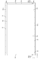
- FIG. 1 is an exploded perspective view showing a schematic configuration of a television receiver TV according to Embodiment 1 of the present invention.
- Rear view of TV receiver TV Exploded perspective view showing a schematic configuration of a liquid crystal display unit LDU constituting the liquid crystal display device A-A 'line cross-sectional view of the liquid crystal display device shown in FIG. B-B 'line sectional view of the liquid crystal display device shown in FIG.
- frame of the state seen from the back side, and a light-guide plate The top view which shows the arrangement
- Enlarged plan view of FIG. The top view which represented typically a mode that the light emitted from the end light source entered into the positioning convex part of the light-guide plate in Embodiment 2.
- FIG. 1 The top view which represented typically a mode that the light emitted from the end light source entered into the positioning convex part of the light-guide plate in Embodiment 3.
- Embodiment 1 of the present invention will be described with reference to FIGS. 1 to 10.
- the television receiver TV and the liquid crystal display device 10 are illustrated.
- Each drawing shows an X-axis, a Y-axis, and a Z-axis, and the directions of the axes are drawn in common directions in the drawings.
- the upper side shown by FIG.3 and FIG.4 be a front side (display surface side), and let the lower side of the figure be a back side (back side).
- FIG. 1 is an exploded perspective view showing a schematic configuration of a television receiver TV according to Embodiment 1 of the present invention
- FIG. 2 is a rear view of the television receiver TV.
- the television receiver TV according to this embodiment includes a liquid crystal display unit LDU, various substrates PWB, MB, and CTB attached to the back side (back side) of the liquid crystal display unit LDU, and a liquid crystal display.
- a cover member CV attached to cover the various substrates PWB, MB, and CTB and a stand ST are provided on the back side of the unit LDU.
- the liquid crystal display unit LDU is supported by the stand ST so that the display surface 11c is along the vertical direction (Y-axis direction).
- the liquid crystal display device 10 is configured by removing at least a configuration for receiving a television signal (such as a tuner portion of the main board MB) from the television receiver TV having the above-described configuration.
- the liquid crystal display unit LDU has a horizontally long rectangular shape as a whole, and includes a liquid crystal panel 11 as a display panel and a backlight device (illumination device) 12 as an external light source, which are external appearances of the liquid crystal display device 10. It is the structure hold
- two stand mounting members STA extending along the Y-axis direction are spaced apart in the X-axis direction. A pair is attached.
- These stand attachment members STA have a substantially channel shape with a cross-sectional shape opened on the surface on the chassis 14 side, and a pair of support columns STb in the stand ST are inserted into a space formed between the stand 14 and the chassis 14. It is configured as follows.
- the wiring member (electric wire etc.) connected to the LED board 18 which the backlight apparatus 12 has passes through the space in the stand attachment member STA.
- the stand ST includes a pedestal portion STa that extends along the X-axis direction and the Z-axis direction, and a pair of support columns STb that rise from the pedestal portion STa along the Y-axis direction.
- the cover member CV is made of synthetic resin, and is attached so as to cover the lower half (see FIG. 2) on the back surface of the chassis 14 while traversing the pair of stand attachment members STA in the X-axis direction. Between the cover member CV and the chassis 14, a space capable of accommodating components such as various substrates PWB, MB, and CTB described later is formed.
- the various substrates PWB, MB, and CTB include a power supply substrate PWB, a main substrate MB, and a control substrate CTB.
- the power supply substrate PWB is a power supply source of the liquid crystal display device 10 and supplies driving power to the other substrates MB and CTB, the LEDs 17 included in the backlight device 12, and the like.
- the main board MB has a tuner section (not shown) that can receive a television signal and an image processing section (not shown) that performs image processing on the received television signal, and sends the processed image signal to the control board CTB. Output.
- the main board MB receives an image signal from the image reproduction device when the liquid crystal display device 10 is connected to an external image reproduction device (not shown).
- the processed signal is output to the control board CTB.
- the control board CTB has a function of converting an image signal input from the main board MB into a liquid crystal driving signal and supplying the converted liquid crystal driving signal to the liquid crystal panel 11.
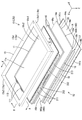
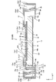
- FIG. 3 is an exploded perspective view showing a schematic configuration of the liquid crystal display unit LDU constituting the liquid crystal display device 10, and FIG. 4 is a cross-sectional view taken along the line AA ′ of the liquid crystal display device 10 shown in FIG.
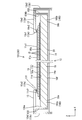
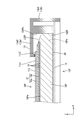
- FIG. 5 is a cross-sectional view of the liquid crystal display device 10 shown in FIG. 3 taken along the line BB ′.
- the liquid crystal display unit LDU constituting the liquid crystal display device 10 includes a frame (front frame) 13 whose main components are arranged on the front side and a chassis arranged on the back side. (Rear chassis) 14 is sandwiched between.
- Major components sandwiched between the frame 13 and the chassis 14 include at least a liquid crystal panel 11, an optical member 15, a light guide plate 16, an LED unit (light source unit) LU, a light source support member 19, A reflection sheet 20 is included.
- the liquid crystal panel 11, the optical member 15, the light guide plate 16, and the reflection sheet 20 are held in a state where they are sandwiched between the front frame 13 and the back chassis 14 in a stacked state.
- the backlight device 12 mainly includes an optical member 15, a light guide plate 16, an LED unit LU, a light source support member 19, a chassis 14, and a reflection sheet 20.
- the LED unit LU is arranged between the frame 13 and the chassis 14 so as to be along the end surface 16 b on the long side of the light guide plate 16.
- the LED unit LU includes an LED (LED light source) 17 that is a light source, and an LED substrate (light source substrate) 18 on which the LED 17 is mounted.
- the LED unit LU is used while being supported by a light source support member (heat radiating member) 19.
- the liquid crystal panel 11 has a horizontally long rectangular shape when seen in a plan view, as shown in FIG.
- the liquid crystal panel 11 has a configuration in which a pair of glass substrates 11a and 11b having excellent translucency are bonded together with a predetermined gap therebetween, and liquid crystal is sealed between the substrates 11a and 11b.
- the front side (display surface 11c side) is a color filter (hereinafter referred to as CF) substrate 11a
- the back side (rear surface 11d side) is an array substrate 11b.
- the array substrate 11b is provided with a switching element (for example, a thin film transistor: TFT) connected to a source wiring and a gate wiring orthogonal to each other, a pixel electrode connected to the switching element, an alignment film, and the like. .
- a switching element for example, a thin film transistor: TFT
- TFT thin film transistor
- a large number of TFTs and pixel electrodes are arranged side by side on the array substrate 11b, and a large number of TFTs and pixel electrodes are arranged around the TFTs and pixel electrodes so as to surround a gate wiring and a source wiring in a lattice shape. It is installed.
- the gate wiring and the source wiring are connected to the gate electrode and the source electrode of the TFT, respectively, and the pixel electrode is connected to the drain electrode of the TFT.
- the array substrate 11b is provided with capacitor wirings (auxiliary capacitor wirings, storage capacitor wirings, Cs wirings) that are parallel to the gate wirings and overlap the pixel electrodes in plan view. Are arranged alternately in the Y-axis direction.
- the CF substrate 11a has a CF in which colored portions such as R (red), G (green), and B (blue) are arranged in a predetermined arrangement, and a lattice frame shape that is arranged so as to partition each CF.
- a light-shielding black matrix hereinafter referred to as BM
- a counter electrode, an alignment film, and the like are provided so as to cover each CF and BM.
- a polarizing plate (not shown) is disposed outside each of the substrates 11a and 11b.
- the array substrate 11b is set to have a larger size in plan view than the CF substrate 11a, as shown in FIGS.
- the array substrate 11b is arranged in such a manner that its end protrudes outward from the end of the CF substrate 11a.
- the array substrate 11b is formed to be slightly larger than the CF substrate 11a so that its outer peripheral end protrudes outside the outer peripheral end of the CF substrate 11a over the entire periphery.
- the pair of long-side end portions constituting the outer peripheral end portion of the array substrate 11b the long-side end portion on the control substrate CTB side (front side shown in FIG. 3, left side shown in FIG.
- a flexible substrate 211 is connected to each source side terminal portion.
- a plurality of flexible substrates 211 are intermittently arranged in the X-axis direction (that is, the direction along the long side end of the array substrate 11b). Each flexible substrate 211 protrudes outward (Y-axis direction) from the end on the long side of the array substrate 11b.
- one of the short side end portions (left side shown in FIG. 3) has the above-described gate wiring and capacitance wiring.
- a plurality of gate-side terminal portions (not shown) routed from are provided.
- a flexible substrate 111 is connected to each gate side terminal portion.
- a plurality of flexible substrates 111 are intermittently arranged in the Y-axis direction (that is, the direction along the short side end of the array substrate 11b).
- Each flexible substrate 111 has a shape that protrudes outward (X-axis direction) from the short-side end of the array substrate 11b.
- the flexible substrate 211 on the source side includes a film-like base material made of a synthetic resin material (for example, polyimide resin) having insulating properties and flexibility, and a source driver (IC for driving a liquid crystal) mounted on the base material. Chip) 212.
- the source driver 212 is disposed on the back side (FIGS. 3 and 4) of the flexible substrate 211.
- a large number of wiring patterns are formed on the base material of the flexible substrate 211, and a source driver 212 mounted near the center of the base material is connected to the wiring patterns.
- the wiring pattern is a conductive path made of a metal film such as a copper foil, and is appropriately formed on the base material of the flexible substrate 211 using a known technique.
- the flexible substrate 211 on which the driver 212 is mounted is configured by so-called SOF (System on Film).
- SOF System on Film
- One end of the flexible substrate 211 is pressure-bonded to the source terminal portion of the array substrate 11b via an anisotropic conductive film (ACF).
- the other end is crimped and connected to a terminal portion (not shown) of the source-side printed board (source board) 213 via an anisotropic conductive film (ACF).
- the printed circuit board 213 and the array substrate 11b (the liquid crystal panel 11) are electrically connected to each other via the flexible substrate 211.
- the printed board (source board) 213 is connected to the control board CTB described above via a wiring member (FPC: flexible printed board) (not shown).
- the printed circuit board 213 supplies signals (scanning signal to the gate wiring, data signal to the source wiring, capacitance signal to the capacity wiring, etc.) input from the control board CTB to the liquid crystal panel 11 side through the flexible substrate 211.
- the printed circuit board 213 has a long shape (band shape). In the case of this embodiment, two printed boards 213 are used, and these are connected to the respective flexible boards 211 so as to be aligned with each other.
- the length of one printed circuit board 213 in the longitudinal direction is set to about half the long side of the liquid crystal panel 11. Further, the length of the printed board 213 in the short direction is longer than the thickness of the light guide plate 16 (the length of the light guide plate 16 in the Z-axis direction) due to the wiring pattern formed on the printed board 213 and the like. ing.
- the flexible substrate 111 on the gate side has a shape in which one end is crimped to the gate side terminal portion of the array substrate 11b via an anisotropic conductive film (ACF).
- the flexible substrate 111 is made of SOF, like the source-side flexible substrate 211.
- a gate driver (IC chip) 112 is mounted on the flexible substrate 111.
- the gate driver 112 is disposed on the back side (FIG. 3) of the flexible substrate 111.
- the array substrate 11b is formed with a relay wiring (not shown) connecting the source side terminal portion and the gate side terminal portion.
- a signal (scanning signal to the gate wiring, capacitance signal to the capacitance wiring, etc.) input from the control substrate CTB is supplied to the gate side terminal portion and the flexible substrate 111 via the relay wiring.
- the liquid crystal panel 11 displays an image on the display surface 11c based on a signal input from the control board CTB.
- the liquid crystal panel 11 is placed on the front side (light emitting side) of the optical member 15 to be described later.
- the plate surface (rear surface 11 d) on the back side of the liquid crystal panel 11 is in close contact with the optical member 15 with almost no gap. This prevents dust and the like from entering between the liquid crystal panel 11 and the optical member 15.
- the display surface (front plate surface) 11c of the liquid crystal panel 11 has a rectangular display area 11c1 on the center side of the screen where images can be displayed, and a frame shape (around the display area on the outer peripheral edge side of the screen). Frame-like non-display area 11c2.
- each terminal part and each flexible substrate 111, 211 described above are arranged in the non-display area 11c2.
- the optical member 15 has a horizontally long rectangular shape as viewed from above, like the liquid crystal panel 11.
- the size (short side dimension and long side dimension) of the optical member 15 is set larger than the display area 11 c 1 of the liquid crystal panel 11.
- the optical member 15 is set to be approximately the same size as the entire liquid crystal panel 11.
- the optical member 15 is placed so as to be laminated on the front side (light emitting side) of the light guide plate 16 described later, and is disposed in a state of being sandwiched between the liquid crystal panel 11 and the light guide plate 16.
- the optical member 15 is sized to fit within the front surface 16 a of the light guide plate 16.
- the optical member 15 is formed by stacking three sheet-like members.
- optical member 15 examples include a diffusion sheet, a lens sheet, a reflective polarizing sheet, and the like, and those appropriately selected from these are used.
- the optical member 15 transmits light emitted from the front surface (light emitting surface) 16a of the light guide plate 16 toward the back surface 11d of the liquid crystal panel.
- the light guide plate 16 is made of a synthetic resin material (for example, acrylic resin such as PMMA or polycarbonate) having a refractive index sufficiently higher than that of air and almost transparent (excellent translucency). As shown in FIG. 3, the light guide plate 16 has a horizontally long rectangular shape when seen in a plane, like the liquid crystal panel 11 and the optical member 15. The light guide plate 16 has a plate shape that is thicker than the optical member 15. The light guide plate 16 has a major side (plate surfaces 16a, 16f) whose long side direction coincides with the X-axis direction, a short side direction coincides with the Y-axis direction, and the main surface (plate surfaces 16a, 16f).
- a synthetic resin material for example, acrylic resin such as PMMA or polycarbonate
- the size of the light guide plate 16 (short side dimension and long side dimension) when viewed from the front side is set larger than that of the liquid crystal panel 11.
- the light guide plate 16 is disposed in the display device 10 such that an end portion of the light guide plate 16 protrudes outward from an end portion of the liquid crystal panel 11.
- the light guide plate 16 is formed to be slightly larger than the liquid crystal panel 11 so that its end protrudes outward from the outer peripheral end of the array substrate 11b of the liquid crystal panel 11 over the entire circumference.
- the light guide plate 16 is disposed on the back side of the optical member 15 and is sandwiched between the optical member 15 and the chassis 14.
- the LED unit LU in a state of being supported by the light source support member 19 is disposed outside the one end surface 16b on the long side of the light guide plate 16, and light from the LED unit LU is transmitted from the end surface 16b to the light guide plate 16. Introduced in.
- the light guide plate 16 has a function of rising and emitting light toward the optical member 15 (front side) while propagating light from the LED unit LU introduced from the end surface 16b on the long side.
- a front-side plate surface (a surface facing the optical member 15) 16 a is a light emitting surface 16 a that emits internal light toward the optical member 15 and the liquid crystal panel 11.
- the end surface 16b on the long side which is long along the X-axis direction, has a predetermined shape with the LED 17 (LED substrate 18).
- the light-incident surfaces 16b are opposed to each other with an interval therebetween, and the light emitted from the LEDs 17 is incident thereon.
- the light incident surface 16b is disposed in parallel along the X-axis direction and the Z-axis direction (the main plate surface of the LED substrate 18), and is substantially orthogonal to the light emitting surface 16a. Further, of the outer peripheral end surface of the light guide plate 16, both short side end surfaces 16d and 16e are arranged in parallel along the Y-axis direction and the Z-axis direction, respectively, and the light incident surface 16b and It is substantially orthogonal to the light exit surface 16a. In the present specification, among the end surfaces of the light guide plate 16, the end surfaces 16d and 16e on the short side may be particularly referred to as side end surfaces 16d and 16e. As shown in FIG. 4, the side end surfaces 16 d and 16 e of the light guide plate 16 are arranged outside the end portion of the liquid crystal panel 11.
- Positioning convex portions 160 are provided on the side end surfaces 16d, 16e of the light guide plate 16, respectively.
- One positioning end 160a is provided on one side end face 16d so as to protrude outward.
- the positioning convex portion 160a is disposed in a portion near the light incident surface 16b in the side end surface 16d that is elongated in the short side direction (Y-axis direction) of the light guide plate 16.
- the positioning convex portion 160a is arranged near the light incident surface 16b.
- the positioning convex portion 160a has a quadrangular shape protruding outward from the side end face 16d.
- one positioning protrusion 160b is provided on the other side end face 16e so as to protrude outward.
- the positioning convex portion 160b is also arranged on the side end surface 16e near the light incident surface 16b.
- the positioning convex portion 160b is disposed near the positioning light incident surface 16b described above.
- the positioning convex portion 160a and the positioning convex portion 160b are provided symmetrically with the light emitting surface 16a interposed therebetween. That is, the positioning convex portions 160 a and 160 b are provided at the same position in the short side direction (Y-axis direction) of the light guide plate 16.
- the positioning convex portion 160 is formed integrally with the other portion of the light guide plate 16 (hereinafter, the main body portion), and is made of the same material as the main body portion. Therefore, the positioning convex portion 160 has the same refractive index as the main body portion of the light guide plate 16.
- the light guide plate 160 provided with the positioning convex portion 160 may be manufactured by cutting a predetermined plate-like member or the like, or manufactured by molding a resin material using a predetermined mold. Also good. The detailed structure of the positioning convex portion 160 will be described later.
- a reflection sheet 20 for reflecting the light in the light guide plate 16 toward the light emitting surface 16 side is disposed on the back side of the light guide plate 16 (that is, the back side of the main body portion of the light guide plate 16).
- the reflection sheet 20 is provided so as to cover the entire plate surface 16 c on the back side of the light guide plate 16.
- the reflection sheet 20 is disposed in the display device 12 so as to be sandwiched between the chassis 14 and the light guide plate 16.
- the reflection sheet 20 is made of a synthetic resin sheet (for example, a foamed polyethylene terephthalate sheet) having a white surface with excellent light reflectivity.
- convex projecting pieces 20a and 20b that are directed to the lower surface of the positioning convex portion 160 are provided at the short side end of the reflective sheet 20 (see FIG. 5).
- At least one of the light exit surface 16a and the back plate surface 16f of the light guide plate 16 is a reflecting portion (not shown) that reflects the light inside the light guide plate 16, or the light inside the light guide plate 16 is scattered.
- the scattering portion (not shown) is patterned so as to have a predetermined in-plane distribution. Accordingly, the light emitted from the light emitting surface 16a is controlled to have a uniform distribution in the surface.
- the LED 17 and the LED substrate 18 constituting the LED unit LU will be described.
- the LED (Light Emitting Diode, light emitting diode) 17 has a configuration in which an LED chip is sealed with a resin material on a substrate portion fixed to the LED substrate 18 as shown in FIGS. 3 and 4. Emits light.
- the LED chip mounted on the substrate unit has a single main emission wavelength. Specifically, those that emit blue light in a single color are used as LED chips.
- a phosphor that emits a predetermined color when excited by blue light emitted from the LED chip is dispersed and blended.
- the resin material is generally configured to emit white light.
- the phosphor for example, a suitable combination of a yellow phosphor that emits yellow light, a green phosphor that emits green light, and a red phosphor that emits red light may be used. They may be used alone.
- the LED 17 is a so-called top emission type in which a surface opposite to the mounting surface with respect to the LED substrate 18 (a surface facing the light incident surface 16b of the light guide plate 16) is a main light emitting surface 17a.
- the light source (LED) 17 of the present embodiment has a Lambertian light distribution.
- the light distribution of the light emitted from the light source (LED) 17 shows a Lambertian light distribution, so that the curve increases as the angle from the optical axis, which is the traveling direction of the light having the highest emission intensity, increases. Therefore, the emission intensity tends to decrease.
- the LED substrate 18 is an elongated plate shape (strip shape, long shape) extending along the long side direction of the light guide plate 16 (X-axis direction, longitudinal direction of the light incident surface 16 b). Shape).
- the LED board 18 is housed in the frame 13 and the chassis 14 with the principal surface thereof in a posture along the X-axis direction and the Z-axis direction (that is, a posture aligned in parallel with the light incident surface 16b of the light guide plate 16). Yes.
- the LED substrate 18 has a length (dimension) in the longitudinal direction set to be substantially the same as the long side of the light guide plate 16.
- the LED 17 is surface-mounted on the plate surface (mounting surface) facing the light guide plate 16 side of the LED substrate 18.
- a plurality of LEDs 17 are arranged in a line on the mounting surface of the LED substrate 18 along the length direction (X-axis direction) with a predetermined interval.
- the distance between the LEDs 17 adjacent in the X-axis direction (that is, the arrangement pitch of the LEDs 17) is set to be approximately equal.
- the arrangement direction of the LEDs 17 coincides with the length direction (X-axis direction) of the LED substrate 18.
- a plurality of LEDs 17 arranged in a row may be referred to as an LED row (light source row) in this specification.
- a metal film for example, copper foil that extends along the longitudinal direction (X-axis direction) of the LED substrate 18 and connects adjacent LEDs 17 across the LEDs 17 in series on the mounting surface of the LED substrate 18.
- a wiring pattern (not shown) is formed. The terminal portions formed at both ends of the wiring pattern are connected to the power supply substrate PWB via wiring members such as connectors and electric wires, so that driving power is supplied to each LED 17.
- the main light emitting surface 17a of each LED 17 mounted on the LED substrate 18 faces the light incident surface 16b of the light guide plate 16, and the optical axis of each LED 17 substantially coincides with the Y-axis direction.
- the base material of the LED substrate 18 is made of metal such as aluminum, for example, and the wiring pattern (not shown) described above is formed on the surface thereof via an insulating layer.
- a white solder resist film (not shown) is formed on the insulating layer so as to cover the wiring pattern.
- insulating materials such as a ceramic, can also be used as a material used for the base material of LED board 18.
- the light source support member (heat radiating member) 19 is made of a metal having excellent thermal conductivity such as aluminum as shown in FIGS.
- the light source support member 19 includes an LED attachment portion (light source attachment portion) 19a to which the LED substrate 18 is attached, and a heat radiating portion 19b in surface contact with the plate surface of the chassis 14, and these have a substantially L-shaped cross section. It has a bent shape.
- the length dimension of the light source support member 19 is set to be approximately the same as the length dimension of the LED substrate 18 described above.
- the LED mounting portion 19 a has a plate shape that is arranged in parallel with the plate surface of the LED substrate 18 and the light incident surface 16 b of the light guide plate 16.
- the long side direction of the LED attachment portion 19a coincides with the X-axis direction
- the short side direction coincides with the Z-axis direction
- the thickness direction coincides with the Y-axis direction.
- the LED board 18 is attached to the inner plate surface (that is, the plate surface facing the light guide plate 16 side) of the LED mounting portion 19a.
- the LED mounting portion 19 a has a long side dimension substantially equal to the long side dimension of the LED substrate 18, but the short side dimension is set to be larger than the short side dimension of the LED substrate 18.
- the outer plate surface (that is, the plate surface opposite to the plate surface on which the LED substrate 18 is mounted) of the LED mounting portion 19a faces an inner wall portion 132 of the frame 13 described later. That is, the LED attachment portion 19 a is arranged in the display device 12 so as to be interposed between the inner wall portion 132 of the frame 13 and the light guide plate 16.
- the LED mounting portion 19a extends along the Z-axis direction (the overlapping direction of the liquid crystal panel 11, the optical member 15, and the light guide plate 16) from the inner end of the heat radiating portion 19b (that is, the end on the LED 17 (light guide plate 16) side). It stands up toward the front side (that is, the frame 13 side). A slight gap is provided between the LED mounting portion 19a and the inner wall portion 132, and the printed circuit board 213 on the source side is accommodated in this gap.
- the heat radiating portion 19 b has a plate shape arranged in parallel to the plate surface of the chassis 14.
- the long side direction of the heat dissipating part 19b coincides with the X-axis direction
- the short side direction coincides with the Y-axis direction
- the thickness direction coincides with the Z-axis direction.
- the heat dissipating part 19b is directed from the back side (lower side) end part (that is, the end part on the chassis 14 side) of the LED mounting part 19a to the outside (that is, opposite to the light guide plate 16 side) along the Y axis direction. Protruding.
- the long side dimension of the heat dissipating part 19b is set to be substantially the same as that of the LED attaching part 19a.
- a plate surface on the back side (lower side) of the heat radiating portion 19 b (that is, a plate surface facing the chassis 14) is in surface contact with the plate surface of the chassis 14.
- board surface (namely, plate surface on the opposite side to the contact surface with respect to the chassis 14) of the front side (upper side) of the thermal radiation part 19b is contacting with the lower end surface of the inner wall part 132 which the flame
- the heat dissipating part 19b is arranged in such a manner as to be sandwiched (intervened) between the inner wall part 132 of the frame 13 and the chassis 14.
- the heat generated with the lighting of the LED 17 is transmitted to the frame 13 having the chassis 14 and the inner wall portion 132 via the LED substrate 18, the LED mounting portion 19 a and the heat radiating portion 19 b.
- the heat radiating portion 19b is provided with an insertion hole 19c through which the screw member SM is passed. The heat radiating portion 19b is fixed to the inner wall portion 132 of the frame 13 using the screw member SM.
- the frame 13 and the chassis 14 are both made of metal such as aluminum, and have high mechanical strength (rigidity), thermal conductivity, and the like.
- the frame 13 and the chassis 14 hold the LED unit LU, and hold a laminate composed of the liquid crystal panel 11, the optical member 15, the light guide plate 16, and the reflection sheet 20 so as to be sandwiched between the front side and the back side.
- the frame 13 has a frame shape surrounding the display area 11c1 on the display surface 11c of the liquid crystal panel 11, and has a horizontally long rectangular shape as a whole.
- the frame 13 mainly includes a frame-shaped facing portion 13a disposed on the front side of the liquid crystal panel 11, an outer wall portion 13b extending from the outer edge portion of the facing portion 13a toward the chassis 14, and an inner edge portion of the facing portion 13a. And projecting toward the liquid crystal panel 11 side, and arranged between the contact portion 13c addressed to the non-display area 11c2 arranged at the periphery of the display area 11c1, and between the outer wall section 13b and the contact section 13c. And inner wall portions 132 and 133 extending from the facing portion 13a toward the chassis 14 side.
- the facing portion 13a is divided into a long facing portion 13a1 disposed on the long side of the frame 13 and a short facing portion 13a2 disposed on the short side thereof.
- the outer wall portion 13b is divided into a long outer wall portion 13b1 disposed on the long side of the frame 13 and a short outer wall portion 13b2 disposed on the long side.
- the contact portion 13c is divided into a long contact portion 13c1 disposed on the long side of the frame 13 and a short contact portion 13c2 disposed on the short side thereof.
- the inner wall part 132 is provided in the long opposing part 13a1, and the inner wall part 133 is provided in the short opposing part 13a2.
- the structure is basically the same as each other.
- the two short side portions provided in the frame 13 basically have the same structure.
- the facing portion 13a is arranged on the front side of the liquid crystal panel 11 so as to cover the non-display area 11c2 on the display surface 11c.
- Each of the long opposing portion 13a1 and the short opposing portion 13a2 has a plate shape having a predetermined thickness that spreads along the plate surface of the chassis 14 (the plate surface of the liquid crystal panel 11).
- the longitudinal contact portion 13c1 provided in the longitudinally facing portion 13a1 is a portion that presses the end portion (non-display area 11c2) on the long side of the liquid crystal panel 11 from the front side toward the chassis 14 (light guide plate 16) side. Yes.
- the longitudinal contact portion 13c1 has an elongated shape along the long side direction of the frame 13 (opposing portion 13a).
- the protruding tip 131 of the longitudinal contact portion 13c1 is made of a light-shielding elastic body (for example, a black rubber elastic body).
- the longitudinal contact portion 13c1 is set such that the tip portion 131 is addressed to the non-display area 11c2 of the liquid crystal panel 11.
- the short contact portion 13c2 provided in the short facing portion 13a2 includes a portion that presses the short side end portion (non-display region 11c2) of the liquid crystal panel 11 from the front side toward the chassis 14 (light guide plate 16) side. It has become.
- the short contact portion 13a2 has an elongated shape along the short side direction of the frame 13 (opposing portion 13a).
- the protruding tip 131 of the short contact portion 13c2 is made of an elastic body having a light shielding property (for example, a black rubber elastic body), like the long contact portion 13c2.
- the short contact portion 13c2 is set so that the tip portion 131 is addressed to the non-display area 11c2 of the liquid crystal panel 11.
- the contact portion 13c generally has a frame shape surrounding the display area 11c1 of the liquid crystal panel 11 and being addressed to the non-display area 11c2.
- the contact portion 13 c provided on the frame 13 sandwiches the laminate with the chassis 14 in a state where the contact portion 13 c is addressed to the non-display area 11 c 2 on the front side periphery of the liquid crystal panel 11.
- the outer wall portion 13b generally surrounds the liquid crystal panel 11 and the like and has a frame shape (cylindrical shape) extending from the facing portion 13a to the chassis 14 side.
- the outer wall part 13b is provided in the outer edge part of the opposing part 13a.
- the outer wall portion 13b is arranged so as to surround the periphery (end surface) of the laminate composed of the liquid crystal panel 11, the optical member 15, the light guide plate 16, and the reflection sheet 20.
- the longitudinal outer wall portion 13 b 1 has a plate shape (wall shape) extending straight from the outer edge portion of the longitudinal facing portion 13 a 1 downward (to the chassis 14 side).
- the short outer wall portion 13b2 has a plate shape (wall shape) extending straight from the outer edge portion of the short facing portion 13a2 downward (to the chassis 14 side).
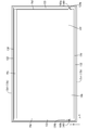
- FIG. 6 is a plan view showing the positional relationship between the frame 13 and the light guide plate 16 as viewed from the back side. As shown in FIG. 6, an outer wall portion 13 b is provided on the periphery of the frame 13 in a square frame shape.
- these inner wall portions 132 and 133 have a rectangular frame shape surrounding the light guide plate 16 as a whole.
- the inner wall 132 on the short side is provided on the frame 13 so as to be along the side end surfaces 16 d and 16 e of the light guide plate 16.
- One inner wall portion 132 arranged outside the side end surface 16d is provided with a recess 134a that fits with the positioning convex portion 160a, and the other inner wall portion 132 arranged outside the side end surface 16e is provided on the other inner wall portion 132.
- a concave portion 134b that fits with the positioning convex portion 160b is provided.
- One inner wall 133 on the long side is arranged outside the light incident surface 16b while maintaining a predetermined distance from the light incident surface 16b.
- the other inner wall portion 133 is disposed outside the end surface 16c while maintaining a predetermined distance from the end surface 16c.
- Grooves 13 d into which the screw members SM can be screwed are formed at the lower end of each inner wall 133.
- FIG. 7 is a plan view showing the positional relationship between the chassis 14 and the light guide plate 16 as viewed from the front side.
- the chassis 14 is generally composed of a horizontally long plate-like member like the liquid crystal panel 11 and the like, and covers the plate surface 16f on the back side of the light guide plate 16 so as to cover the liquid crystal display unit LDU (liquid crystal display). Arranged on the back side of the device 10).
- the chassis 14 has a plate-like bottom plate 14a having a rectangular shape, standing wall plates 14b and 14c erected at the end of the long side of the bottom plate 14a, and the opposite side of the bottom plate 14a from these standing wall plates 14b and 14c. Overhang plates 141b and 141c projecting toward (outside) are provided.
- the bottom plate 14 a is a portion addressed to the plate surface 16 f on the back side of the light guide plate 16 through the reflection sheet 20 and occupies most of the chassis 14.
- the bottom plate 14 a is in close contact with the plate surface 16 f on the back side of the light guide plate 16 through the reflection sheet 20.
- the standing wall plates 14b and 14c are provided at respective end portions on the long side of the bottom plate 14a.
- Each of the standing wall plates 14b, 14c and the bottom plate 14a is made of a plate-like member having a thickness comparable to that of the standing wall plates 14b, 14c.
- the standing wall plates 14b and 14c are erected from the bottom plate 14a toward the side opposite to the liquid crystal panel 11 side at the end portion on the long side of the bottom plate 14a.
- the standing wall plates 14b and 14c are formed in a plate shape (wall shape) extending elongated along the long side direction of the bottom plate 14a.
- the standing wall plates 14b and 14c are arranged on the inner side of the end surfaces 16b and 16c on the long side of the light guide plate 16 as shown in FIG.
- Overhang plates 141b and 141c are provided from these standing wall plates 14b and 14c toward the opposite side (outside) of the bottom plate 14a.
- the overhanging plates 141b and 141c are formed of a plate-like member that is elongated along the long side direction of the bottom plate 14a and has the same thickness as the bottom plate 14a. It should be noted that the outer edge portions of the projecting plates 141b and 141c rise toward the upper side (the liquid crystal panel 11 side), and the raised portions are set so as to be arranged inside the longitudinal outer wall portion 13b1.
- the overhanging plates 141b and 141c are opposed to the longitudinally facing portion 13a1 as shown in FIG. Further, the overhanging plates 141 b and 141 c are portions where the heat radiating portion 19 b of the light source support member 19 contacts. The overhanging plates 141b and 141c are portions facing the inner wall portion 132 through the heat radiating portion 19b.
- the frame 13 is set on a predetermined work table.
- the frame 13 on the work table is in a state where the front side faces the lower side (work table side) and the back side faces the upper side. That is, the frame 13 is set upside down on the work table.
- the liquid crystal panel 11 is assembled on the upper side of the frame 13 on the work table (that is, the back side of the frame 13).
- the liquid crystal panel 11 is in a state in which the CF substrate 11a is disposed on the lower side (workbench side) and the array substrate 11b side is disposed on the upper side.
- the contact portion 13c of the frame 13 is in a state of being addressed to the non-display area 11c2 of the liquid crystal panel 11.
- the optical member 15 is placed on the back side (the back surface 11 d side) of the liquid crystal panel 11.
- the LED unit LU supported by the light source support member 19 is disposed on the frame 13 side.
- the light guide plate 16 is placed on the optical member 15.
- the positioning convex portion 160a provided on one side end surface 16d of the light guide plate 16 is fitted into the concave portion 134a provided on the frame 13, and the positioning convex portion provided on the other side end surface 16e.
- the shaped part 160 b is fitted into a concave part 134 b provided in the frame 13.
- the front surface 16a (light emitting surface) 16a of the light guide plate 16 is disposed on the lower side, and the rear surface 16f is disposed on the upper side.
- the reflection sheet 20 is assembled on the plate surface 16 f on the back side of the light guide plate 16.
- the chassis 14 is assembled to the frame 13 side.
- Each component of the liquid crystal display unit LDU is assembled by fixing the chassis 14 to the frame 13 using a screw member SM or the like. Thereafter, the stand mounting member STA and the various substrates PWB, MB, and CTB are assembled on the back surface side of the liquid crystal display unit LDU, and the stand ST and the cover member CV are further assembled. The display device 10 and the television receiver TV are manufactured.
- each LED 17 constituting the backlight device 12 is driven to turn on.
- each LED 17 is driven and light is emitted from each LED 17, light is incident on the inside from the light incident surface 16 b of the light guide plate 16.
- the incident light is reflected by the reflection sheet 20 laid on the back side of the light guide plate 16 and travels through the light guide plate 16, and from the front side plate surface (light emitting surface 16 a) toward the optical member 15. Emitted.
- the emitted light passes through the optical member 15 and becomes light that spreads substantially uniformly in a planar shape, and irradiates the back surface 11 d of the liquid crystal panel 11.
- the liquid crystal panel 11 displays an image on the display area 11c1 of the display surface 11c by using the light spread in a planar shape.
- the light guide plate 16 of the present embodiment includes positioning convex portions 160a and 160b on the side end surfaces 16d and 16e, respectively. These positioning convex portions 160a and 160b are provided on the side end surfaces 16d and 16e at portions close to the light incident surface 16b.
- the light guide plate 16 is fixed in the liquid crystal display device 10 using the positioning convex portions 160a and 160b.
- each positioning convex-shaped part 160a, 160b is provided in the part near the light-incidence surface 16b in each side end surface 16d, 16e, when the light-guide plate 16 thermally expands, the light-incidence surface 16b will be LED. Contact with each LED 17 of the unit LU is suppressed.
- the length of the light guide plate 16 (the length in the Y-axis direction) between the light incident surface 16b and the positioning convex portions 160a and 160b is very short, and the portion is almost in the Y-axis direction. This is because the thermal expansion does not occur. As a result, the light incident surface 16b is suppressed from moving in the direction approaching the LED 17. Note that when the light guide plate 16 is thermally expanded, the end surface 16c moves mainly from the positioning convex portions 160a and 160b in a direction approaching the outer inner wall portion 132.
- the distance between the LED 17 and the light incident surface 16b can be kept short and substantially constant, and the light emitted from each LED 17 is guided from the light incident surface 16b.
- the efficiency (light incident efficiency) incident on the light plate 16 can be easily controlled and the efficiency can be increased.
- the positioning convex portion 160 when the positioning convex portion 160 is disposed near the light incident surface 16b of the light guide plate 16, light emitted from the LED 17 enters the positioning convex portion 160.
- light emitted from an LED hereinafter referred to as an end light source
- positioning convex portion 160 side among LED rows (light source rows) 170 in which a plurality of LEDs 17 are arranged in a row
- end light source located on the most end side (positioning convex portion 160 side) among LED rows (light source rows) 170 in which a plurality of LEDs 17 are arranged in a row
- the positioning convex portion 160 conventionally, the light leaks from the positioning convex portion, and the leaked light enters the liquid crystal panel from the end portion and forms a streak on the display surface (search light shape). Brightness unevenness was generated.
- the liquid crystal display device 10 of the present embodiment even when light emitted from the LED 17 enters the positioning convex portion 160, the above-described luminance unevenness is suppressed from occurring on the display surface 11c of the liquid crystal panel 11. ing.
- FIGS. In the following description, for the sake of convenience, a state in which the light guide plate 16 is viewed from the front side will be described as an example.
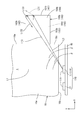
- FIG. 8 is a plan view schematically showing a state in which the light L2 emitted from the end light source 17X enters the positioning convex portion 160b of the light guide plate 16.
- FIG. 8 schematically shows the structure of the light guide plate 16 in the vicinity where the positioning convex portion 160b is provided.
- the recessed part 134b etc. which fit the positioning convex part 160b are abbreviate
- the LED row (light source row) 170 is mounted on the plate surface of the LED substrate 18 so as to face the light incident surface 16 b of the light guide plate 16.
- the LED 17 arranged on the rightmost side (positioning convex portion 160b side) is the end light source 17X.
- the LED 17 disposed on the leftmost side (that is, the positioning convex portion 160a side) in the LED row 170 is also an end light source for the positioning convex portion 160a.
- the relationship between the positioning convex portion 160b and the end light source 17X with respect to the positioning convex portion 160b will be described as an example.
- the optical axis of the end light source 17X is indicated by a symbol L1.
- the optical axis L1 is shown as a light beam extending straight from the center of the main light emitting surface 17a toward the light incident surface 16b side.
- the optical axis L1 intersects perpendicularly with respect to the light incident surface 16b and is disposed in parallel with the side end surface 16e.
- the position of the end light source 17 (the position in the X-axis direction) is set so that the optical axis L1 intersects with the light incident surface 16b at least when the light guide plate 16 is viewed from the front side.
- the light emitted from the end light source 17X proceeds in the direction of the angle ⁇ outward (to the positioning convex portion 160b side) with respect to the optical axis L1.
- Light L2 is shown.
- This angle ⁇ is set to the same size as the critical angle ⁇ c at the boundary surface between the light guide plate 16 and the outside air.
- the light guide plate 16 is made of an acrylic resin, and the critical angle ⁇ c is 42.2 °. Therefore, in the present embodiment, the angle ⁇ described above is 42.2 °.
- the angle ⁇ means an angle between the optical axis L1 and the light L2 after entering the light guide plate 16.
- light traveling in the direction of the angle ⁇ outward from the optical axis L1 may be particularly referred to as narrow-angle light.
- the positioning convex portion 160b is provided on the side end face 16e of the light guide plate 16 at a position where the above-described narrow-angle light L2 enters.
- the narrow-angle light L2 emitted from the end light source 17X passes through the light guide plate 16. While proceeding, it goes directly into the positioning convex portion 160b.
- a first end surface 161b (161), a second end surface 162b (162), and a third end surface 163b (163) are disposed around the positioning convex portion 160b.
- the positioning convex portion 160b includes a front surface 164b (164) and a back surface 165b (165) which are adjacent to the end surfaces 161b, 162b, 163b in a state perpendicular to the end surfaces 161b, 162b, 163b.
- 1st end surface 161b consists of an end surface distribute
- the first end surface 161 b is arranged in parallel to the side end surface 16 e of the light guide plate 16.
- the first end surface 161b is also arranged in parallel to the optical axis L1 of the end light source 17X.
- 2nd end surface 162b consists of an end surface distribute
- the second end surface 162b is arranged in parallel to the light incident surface 16b.
- the second end surface 162b is adjacent to the first end surface 161b in a state perpendicular to the first end surface 161b.
- the length (the length in the X-axis direction) of the second end face 162b when the light guide plate 16 is viewed from the front side is a length such that the narrow-angle light L2 entering the positioning convex portion 160b directly hits it. Is set.
- the length of the second end face 162b is set so that the narrow-angle light L2 does not directly hit the first end face 161b.
- the length of the second end surface 162b is set longer than the length of the first end surface 161b. Therefore, the positioning convex portion 160b has a horizontally long rectangular shape when viewed from the front side of the light guide plate 16.
- 3rd end surface 163b consists of an end surface distribute
- the third end surface 163b is disposed closer to the light incident surface 16b than the second end surface 162b.
- the third end surface 163b is arranged in parallel to the second end surface 162b and the light incident surface 16b. Note that the light emitted from the end light source 17X does not directly hit the third end surface 163b because of the arrangement relationship.
- the arrangement relationship between the end light source 17X and the positioning convex portion 160b is appropriately set so as to satisfy the optical conditions described later.
- the position of the end light source 17X in the X-axis direction may be set so that the distance from the side end surface 16e to the optical axis 11 of the end light source 17X is equal to or shorter than the length of the first end surface 161b.
- the above-described narrow-angle light L2 is incident on the second end face 162b at an angle ⁇ (that is, a critical angle ⁇ c). Therefore, the narrow-angle light L2 is totally reflected at the second end face 162b. Accordingly, the narrow-angle light L2 is prevented from leaking outside from the second end face 162b.
- the light L12 traveling outward from the optical axis L1 in the direction of the angle ⁇ ′ ( ⁇ c) smaller than the angle ⁇ is directly irradiated to the second end surface 162b
- the light L12 is incident on the second end face 162b at an angle ⁇ ′ (that is, an angle smaller than the critical angle ⁇ c). Therefore, the light L12 passes through the second end surface 162b while being refracted by the second end surface 162b and leaks outside.
- the light L122 leaking from the second end face 162b is directed outward so as to be separated from the liquid crystal panel 11, but not directed toward the liquid crystal panel 11.
- the light emitted from the end light source 17X when light is incident on the second end surface 162b at an angle larger than the angle ⁇ , the light is totally reflected by the second end surface 162b. Therefore, it is possible to prevent light from leaking from the second end face 162b toward the end of the liquid crystal panel 11. That is, even if the light emitted from the end light source 17X is applied to the second end surface 162b, the light is suppressed from entering from the end portion (end surface) of the liquid crystal panel 11 toward the inside thereof.
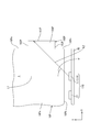
- FIG. 9 is a plan view schematically showing how the other light L3 emitted from the end light source 17X enters the positioning convex portion 160b of the light guide plate 16, and FIG. 10 is an enlarged plan view of FIG. It is.
- the light L3 traveling outward in the direction of the angle ⁇ from the optical axis L1 is directly applied to the first end surface 161b of the positioning convex portion 160b.
- the angle ⁇ is set larger than the angle ⁇ ( ⁇ c), and is set to 50 °, for example.
- the light L13 having an incident angle larger than the light L3 described above that is, the incident angle with respect to the first end surface 161b is greater than or equal to the critical angle ⁇ c.
- the light L13 is totally reflected by the first end face 161b.
- the angle ⁇ ′ is set to 45 °, for example.
- the light L131 reflected by the first end face 161b also enters the second end face 162b at an angle equal to or greater than the critical angle ⁇ c. That is, the light L131 is totally reflected by the second end surface 162b.
- the light L132 reflected by the second end face 162b is returned to the main body portion of the light guide plate 16 while proceeding through the positioning convex portion 160b. Therefore, even if the light emitted from the end light source 17X is totally reflected by the first end surface 161b, the light is prevented from leaking so as to approach the end of the liquid crystal panel 11 from the second end surface 162b.
- the angle ⁇ described above is preferably 45 ° or more. If the light emitted from the end light source 17X has an incident angle with respect to the first end face 161b of 45 ° or less, the light is either totally reflected by the first end face 161b and the first end face 162b, or the first It is refracted at the end face 161b and transmitted to the outside, and the occurrence of uneven brightness in the liquid crystal panel 11 is suppressed.
- the positioning convex portion 160b As described above, even if the light emitted from the end light source 17X enters the positioning convex portion 160b, the entering light is prevented from leaking toward the end portion (end surface) of the liquid crystal panel 11. Similarly, the other positioning convex portion 160a is prevented from leaking light toward the end portion (end surface) of the liquid crystal panel 11.
- the positioning convex portion 160a and the positioning convex portion 160b have a symmetrical structure with respect to the main body portion of the light guide plate 16.
- the positioning convex portion 160 (160a, 160b) of the light guide plate 16 has a predetermined shape, so that the positioning convex portion 160 (160a, 160b) The leaked light is prevented from entering the inside from the end surface (end portion) of the liquid crystal panel 11 and causing streaky (searchlight-like) luminance unevenness on the display surface 11c.
- the length of the second end face 162b of the positioning convex portion 160 is preferably equal to or longer than the length of the first end face 161b.
- the length of the second end surface 162b is set longer than the length of the first end surface 161b.
- the length of the second end surface 162b may be the same as the length of the first end surface 161b.
- the shape of the positioning convex portion 160 may be a square.
- the light guide plate 16 is made of acrylic resin (PMMA).
- PS polystyrene
- MS methyl methacrylate / styrene
- PC polycarbonate
- the critical angle ⁇ c of the light guide plate is approximately 40.8 °.
- the critical angle ⁇ c of the light guide plate 16 is usually 43 ° or less, although it varies slightly depending on the material used. Therefore, the angle ⁇ described above is preferably 43 ° or less.
- FIG. 11 is a plan view schematically showing a state in which light L2 emitted from the end light source 17X enters the positioning convex portion 160Ab of the light guide plate 16A in the second embodiment.
- the light guide plate 16A of the present embodiment has the same configuration as that of the light guide plate 16 of the first embodiment except that the shape of the positioning convex portion 160Ab is different from that of the first embodiment.
- the positioning convex portion 160Ab includes a first end surface 161Ab, a second end surface 162Ab, and a third end surface 163Ab, and also includes a front surface 164Ab and a back surface 165Ab.
- the length of the second end surface 162Ab of the positioning convex portion 160Ab is shorter than the length of the first end surface 161Ab.
- the second end surface 162Ab is secured to have a length such that the narrow-angle light L2 emitted from the end light source 17X directly hits the same as in the first embodiment.
- the length of the second end face 162Ab is at least as long as the narrow-angle light L2 directly hits it. It only has to be.
- the installation location of positioning convex-shaped part 160Ab in the side end surface 16e is adjusted suitably.
- the position of the end light source 17X (position in the X-axis direction) is also set as appropriate so that the narrow-angle light L2 does not directly hit the first end surface 161Ab.
- the length of the second end face is set to be equal to or greater than the length of the first end face as in the first embodiment.
- FIG. 12 is a plan view schematically showing a state in which the light L2 emitted from the end light source 17X enters the positioning convex portion 160Bb of the light guide plate 16B in the third embodiment.
- the light guide plate 16B of the present embodiment has the same configuration as the light guide plate 16 of the first embodiment except that the shape of the positioning convex portion 160Bb is different from that of the first embodiment.
- the positioning convex portion 160Bb of the present embodiment has a square shape when the light guide plate 16B is viewed from the front side.
- the length of the second end surface 162Bb when the light guide plate 16B is viewed from the front side is set to be the same as the length of the first end surface 161Bb.
- the narrow-angle light L2 emitted from the end light source 17X is set so as to irradiate the portion (corner portion) where the first end surface 161Bb and the second end surface 162Bb intersect.
- the shape of the positioning convex portion 160Bb may be a square.
- FIG. 13 is a plan view schematically showing a state where light emitted from the end light source 17X enters the positioning convex portion 160P of the light guide plate 16P in the comparative example
- FIG. 14 is an enlarged plan view of FIG.
- FIG. 15 is an explanatory view schematically showing how light leaks from the positioning convex portion 160P of the light guide plate 16P toward the end portion of the liquid crystal panel 11 in the liquid crystal display device 10P in the comparative example. .
- liquid crystal display device 10P of the comparative example is different from the first embodiment etc. in the configuration of the positioning convex portion 160P of the light guide plate 16P and the structure of the concave portion 134Pb and the like fitted to the positioning convex portion 160P, Other configurations are the same as those in the first embodiment.
- the narrow-angle light L2 emitted from the end light source 17X is directly irradiated onto the first end surface 161P of the positioning convex portion 160P. That is, in this comparative example, the length of the second end surface 162P of the positioning convex portion 160P when the light guide plate 16P is viewed from the front side is shorter than the first end surface 161b and the like of each embodiment. The length is such that the angular light L2 does not directly hit.
- FIG. 14 shows light L2P traveling outward from the optical axis L1 in the direction of an angle ⁇ ′′ ( ⁇ c) smaller than the angle ⁇ of the narrow-angle light L2.
- FIG. 14 shows a plan view from the front side of the light guide plate 16P, and shows the state where the light L22P travels toward the side end face 16Pe of the light guide plate 16P.
- the light leaks outward from the second end surface 162P of the positioning convex portion 162P, and light traveling toward the end surface of the liquid crystal panel 11 is generated.
- the light traveling toward the end of the liquid crystal panel 11 such as the light L22P enters the display surface 11 (display region 11c1) inside the liquid crystal panel 11 from the end (end surface). Then, streaky (searchlight-like) luminance unevenness appears on the display surface 11c (display region 11c1) of the liquid crystal panel, and a display defect occurs in the liquid crystal display device 10P.
- the shape of the positioning convex portion 160P of the light guide plate 16P is different from that of the above-described embodiment, luminance unevenness occurs in the liquid crystal panel.
- light is incident from one end face of the light guide plate. In other embodiments, light is incident from two or more end faces into the light guide plate. It may be.
- one positioning convex portion is provided on each of the two side end surfaces of the light guide plate. In other embodiments, two or more positioning portions are provided on one side end surface. A convex portion may be provided.
- two positioning convex portions are provided for one light guide plate.
- one positioning convex portion is provided for one light guide plate.
- the structure provided may be sufficient.
- another light guide plate positioning method for example, a locking pin erected on the chassis is inserted in the thickness direction of the light guide plate. Etc. may be used.
- the number and arrangement of LED substrates, the number and arrangement of LEDs mounted on the LED substrate, and the like can be changed as appropriate without departing from the object of the present invention.
- the liquid crystal panel and the chassis are illustrated in a vertically placed state in which the short side direction coincides with the vertical direction.
- the liquid crystal panel and chassis coincide with the long side direction in the vertical direction. What was made into the vertically placed state made into the above is also contained in this invention.
- the TFT is used as the switching element of the liquid crystal display device.
- the present invention can also be applied to a liquid crystal display device using a switching element other than the TFT (for example, a thin film diode (TFD)).
- a switching element other than the TFT for example, a thin film diode (TFD)
- the present invention can also be applied to a liquid crystal display device that performs monochrome display.
- the television receiver provided with the tuner is exemplified, but the present invention is also applicable to a display device not provided with the tuner.
- an optical member or a reflection sheet may not be provided.
- SYMBOLS 10 Liquid crystal display device (display device), 11 ... Liquid crystal panel (display panel), 11a ... Color filter substrate, 11b ... Array substrate, 11c ... Display surface, 11c1 ... Display region, 11c2 ... Non-display region, 11d ... Back surface, DESCRIPTION OF SYMBOLS 12 ... Backlight apparatus (illuminating device), 13 ... Frame, 13a ... Opposite part, 13b ... Outer wall part, 13c ... Contact part, 134a, 134b ... Recessed part, 14 ... Chassis, 15 ... Optical member (optical sheet), 16 ... Light guide plate, 16a ...
Landscapes
- Physics & Mathematics (AREA)
- General Physics & Mathematics (AREA)
- Optics & Photonics (AREA)
- Nonlinear Science (AREA)
- Engineering & Computer Science (AREA)
- Mathematical Physics (AREA)
- Crystallography & Structural Chemistry (AREA)
- Chemical & Material Sciences (AREA)
- Multimedia (AREA)
- Signal Processing (AREA)
- Microelectronics & Electronic Packaging (AREA)
- Planar Illumination Modules (AREA)
- Liquid Crystal (AREA)
Abstract
表示装置10は、表示パネル11、光源列170、導光板16、シャーシ14、シャーシ14に宛がわれる凹部134bを備える。導光板16は、凹部134bと嵌合する位置決め凸状部160を有する。凸状部160は、導光板16の側端面16eから外側に向かって突出する形をなし、光源列170の端光源17Xからの光のうち光入射面16bから入射して光軸L1に対して外側に角度α(臨界角θc)の方向に進む狭角光L2が入り込む凸状部からなり、側端面16eに対して平行に配され狭角光L2が当たらない位置に配される第1端面161と、側端面16eと第1端面161の間に配され光入射面16bに対して平行に配されつつ狭角光L2が当たる位置に配される第2端面162を含む。
Description
本発明は、表示装置、及びテレビ受信装置に関する。
テレビ、携帯電話、携帯情報端末等の表示装置に、液晶パネルが汎用されている。液晶パネルは、それ自身で光を発することができないため、画像を表示させるために、照明装置(所謂、バックライト装置)の光を利用している。この照明装置は、液晶パネルの背面側に配され、液晶パネルの背面に向けて面状の光を出射するように構成されている。
前記照明装置としては、特許文献1に示されるように、導光板と、この導光板の端面と対向する対向するように配される光源とを備えるものが知られている。この種の照明装置は、一般的に、サイドライト型(又はエッジライト型)として知られており、導光板の端面が、光源から発せられた光が入射される光入射面となっており、そして、導光板の表側の板面が、液晶パネルの背面に向けて光を出射する光出射面となっている。
なお、液晶パネルは、一般的に、その表側の周縁に被せられる金属製の枠状部材と、その背面側の周縁に宛がわれる遮光性を備えたプラスチック製の枠状部材との間で挟まれた状態で、前記照明装置の光出射面側に配されている。
しかしながら、近年、薄型化等の要望により、液晶パネルの背面側に配される上述した枠状部材を省略した構成の表示装置が提案されている。この種の表示装置において、液晶パネルは、導光板の表側の板面上に載せられる形で設置されている。
また、特許文献2に示されるように、導光板の側端面に設けられている凸状部を利用して、照明装置内で導光板を固定する構成が知られている。なお、近年、上述した照明装置の光源として、複数個のLEDを列状に並べたもの(以下、LED列)が、従来の冷陰極管に替わって用いられている。
(発明が解決しようとする課題)
上述した凸状部を利用して導光板が固定されている照明装置において、光源から発せられた光が凸状部内に入り込むと、その光が凸状部から外側に漏れ出して、更に液晶パネルの端面からその内側に入り込んでしまうことがある。液晶パネルの端面から内側に光が入り込んでしまうと、液晶パネルの表示面にスジ状の輝度ムラが発生してしまい、問題となっている。例えば、液晶パネルが黒表示の場合であっても、液晶パネルの端面から光が入り込んでしまうと、表示面に周囲よりも輝度が高すぎるスジ状の輝部が表示されてしまい、問題となっている。
上述した凸状部を利用して導光板が固定されている照明装置において、光源から発せられた光が凸状部内に入り込むと、その光が凸状部から外側に漏れ出して、更に液晶パネルの端面からその内側に入り込んでしまうことがある。液晶パネルの端面から内側に光が入り込んでしまうと、液晶パネルの表示面にスジ状の輝度ムラが発生してしまい、問題となっている。例えば、液晶パネルが黒表示の場合であっても、液晶パネルの端面から光が入り込んでしまうと、表示面に周囲よりも輝度が高すぎるスジ状の輝部が表示されてしまい、問題となっている。
本発明の目的は、導光板の側端面に設けられている位置決め凸状部から漏れ出した光が、表示パネル内に端面から入り込むことが抑制された表示装置等を提供することである。
(課題を解決するための手段)
本実施形態に係る表示装置は、表示面を表側に含む表示パネルと、複数の光源が列状に並んでなる光源列と、板状部材であって、前記板状部材の端面からなり前記光源列と対向しつつ各光源からの光が入射される光入射面と、前記板状部材の表側の板面からなり前記表示パネルの裏側に向けて光を出射する光出射面と、前記光入射面に隣接する前記板状部材の端面からなり前記光入射面に対して略直交しつつ前記表示パネルの端部よりも外側に配される側端面と、前記側端面のうち前記光入射面寄りの部分に設けられ、前記側端面から外側に向かって突出する形をなし、かつ前記光源列の端に配される端光源から発せられた光のうち前記光入射面から入射して前記端光源の光軸に対して外側に角度α(但し、角度αは板状部材の臨界角θcと同じ大きさ)の方向に進む狭角光が入り込む凸状部からなり、前記側端面から最も外側に離れた前記凸状部の端面からなり前記側端面に対して平行に配されつつ前記狭角光が当たらない位置に配される第1端面と、前記側端面と前記第1端面との間に配される前記凸状部の端面からなり前記光入射面に対して平行に配されつつ前記狭角光が当たる位置に配される第2端面とを含む位置決め凸状部と、を有する導光板と、内側に前記位置決め凸状部が納まる形で前記導光板の裏側を覆う板状のシャーシと、前記位置決め凸状部と嵌合すると共に、前記シャーシに対して位置決めされた状態で宛がわれる凹部と、を備える。
本実施形態に係る表示装置は、表示面を表側に含む表示パネルと、複数の光源が列状に並んでなる光源列と、板状部材であって、前記板状部材の端面からなり前記光源列と対向しつつ各光源からの光が入射される光入射面と、前記板状部材の表側の板面からなり前記表示パネルの裏側に向けて光を出射する光出射面と、前記光入射面に隣接する前記板状部材の端面からなり前記光入射面に対して略直交しつつ前記表示パネルの端部よりも外側に配される側端面と、前記側端面のうち前記光入射面寄りの部分に設けられ、前記側端面から外側に向かって突出する形をなし、かつ前記光源列の端に配される端光源から発せられた光のうち前記光入射面から入射して前記端光源の光軸に対して外側に角度α(但し、角度αは板状部材の臨界角θcと同じ大きさ)の方向に進む狭角光が入り込む凸状部からなり、前記側端面から最も外側に離れた前記凸状部の端面からなり前記側端面に対して平行に配されつつ前記狭角光が当たらない位置に配される第1端面と、前記側端面と前記第1端面との間に配される前記凸状部の端面からなり前記光入射面に対して平行に配されつつ前記狭角光が当たる位置に配される第2端面とを含む位置決め凸状部と、を有する導光板と、内側に前記位置決め凸状部が納まる形で前記導光板の裏側を覆う板状のシャーシと、前記位置決め凸状部と嵌合すると共に、前記シャーシに対して位置決めされた状態で宛がわれる凹部と、を備える。
前記表示装置において、導光板は、位置決め凸状部を有している。位置決め凸状部は、導光板における側端面のうち光入射面寄りの部分に設けられ、前記側端面から外側に向かって突出する形をなし、かつ前記端光源から発せられた光のうち前記光入射面から入射して前記端光源の光軸に対して外側に角度αの方向に進む狭角光が入り込む部分となっている。なお、前記角度αは、板状部材(導光板)の臨界角θcと同じ大きさとなっている。また、位置決め凸状部は、前記側端面から最も外側に離れた端面からなり前記側端面に対して平行に配されつつ前記狭角光が当たらない位置に配される第1端面と、前記側端面と前記第1端面との間に配される端面からなり前記光入射面に対して平行に配されつつ前記狭角光が当たる位置に配される第2端面とを含んでいる。このような前記表示装置において、前記端光源から発せられた光のうち前記光入射面から入射して前記端光源の光軸に対して外側に角度αの方向に進む狭角光が前記第2端面に当たると、前記狭角光は前記第2端面で屈折しつつ前記第2端面を透過して前記側端面から離れる方向に向かって進む。また、前記端光源から発せられた光のうち前記光入射面から入射して記位置決め凸状部内を進みつつ前記第1端面で反射された反射光は、前記第2端面に対して、常に、臨界角θcよりも大きな角度で入射することになる。その結果、その反射光は、前記第2端面で全反射されることになり、前記第2端面から外側に漏れ出すことが抑制される。つまり、端光源から発せられた光が位置決め凸状部内に入り込んで、第1端面又は第2端面に照射されても、これらの端面から表示パネルの端部が配されている導光板の側端面側に向かって光が漏れ出すことが抑制される。その結果、表示パネルの端部から光が侵入して表示パネルの表示面にスジ状の輝度ムラが発生することが抑制される。
前記表示装置において、前記導光板を表側から平面視した場合において、前記第2端面の長さは、前記第1端面の長さ以上に設定されていることが好ましい。
前記表示装置において、前記端光源から発せられた光のうち、前記光入射面から入射して前記位置決め凸状部内を進みつつ前記第1端面に対して入射する光の角度が45°以下であることが好ましい。
前記表示装置において、前記角度αは、43°以下であることが好ましい。
前記表示装置において、前記導光板は、PMMA(ポリメチルメタクリレート)材料、PS(ポリスチレン)材料、MS(メチルメタクリレート・スチレン)材料及びPC(ポリカーボネート)材料から選ばれる1つの材料からなるものが好ましい。
前記表示装置において、前記光源は、ランバーシアン型の配光分布を有する発光ダイオードからなるものであってもよい。
前記表示装置において、前記光源は、白色発光ダイオードであるものであってもよい。
前記表示装置において、前記導光板を表側から平面視した場合において、前記側端面から前記端光源の前記光軸までの距離は、前記第1端面の長さ以下であってもよい。
前記表示装置において、前記表示パネルは、一対の基板間に液晶を封入してなる液晶パネルからなるものであってもよい。
本実施形態に係るテレビ受信装置は、前記表示装置を備える。
(発明の効果)
本発明によれば、導光板の側端面に設けられている位置決め凸状部から漏れ出した光が、表示パネル内に端面から入り込むことが抑制された表示装置等を提供することができる。
本発明によれば、導光板の側端面に設けられている位置決め凸状部から漏れ出した光が、表示パネル内に端面から入り込むことが抑制された表示装置等を提供することができる。
<実施形態1>
本発明の実施形態1を、図1から図10を参照しつつ説明する。本実施形態では、テレビ受信装置TV、及び液晶表示装置10を例示する。なお、各図面には、X軸、Y軸及びZ軸が示されており、各軸方向が各図面において共通の方向となるように描かれている。また、図3及び図4に示される上側を表側(表示面側)とし、同図下側を裏側(背面側)とする。
本発明の実施形態1を、図1から図10を参照しつつ説明する。本実施形態では、テレビ受信装置TV、及び液晶表示装置10を例示する。なお、各図面には、X軸、Y軸及びZ軸が示されており、各軸方向が各図面において共通の方向となるように描かれている。また、図3及び図4に示される上側を表側(表示面側)とし、同図下側を裏側(背面側)とする。
図1は、本発明の実施形態1に係るテレビ受信装置TVの概略構成を示す分解斜視図であり、図2は、テレビ受信装置TVの背面図である。本実施形態に係るテレビ受信装置TVは、図1に示されるように、液晶表示ユニットLDUと、この液晶表示ユニットLDUの裏側(背面側)に取り付けられる各種基板PWB,MB,CTBと、液晶表示ユニットLDUの裏側に、各種基板PWB,MB,CTBを覆う形で取り付けられるカバー部材CVと、スタンドSTとを備えている。液晶表示ユニットLDUは、その表示面11cが鉛直方向(Y軸方向)に沿うように、スタンドSTによって支持されている。
本実施形態に係る液晶表示装置10は、上記した構成のテレビ受信装置TVから、少なくともテレビ信号を受信するための構成(メイン基板MBのチューナー部等)を除いたものからなる。液晶表示ユニットLDUは、全体として横長の矩形状をなしており、表示パネルとしての液晶パネル11と、外部光源としてのバックライト装置(照明装置)12とを備え、これらが液晶表示装置10の外観を構成するフレーム13及びシャーシ14によって一体的に保持された構成となっている。
液晶表示装置10における裏側の外観を構成するシャーシ14の裏面には、図2に示されるように、Y軸方向に沿って延在する形態のスタンド取付部材STAがX軸方向に離間した二個所に一対取り付けられている。これらスタンド取付部材STAは、断面形状がシャーシ14側の面が開口した略チャンネル型をなしており、シャーシ14との間に形成される空間内に、スタンドSTにおける一対の支柱部STbが差し込まれるように構成されている。なお、スタンド取付部材STA内の空間には、バックライト装置12が有するLED基板18に接続された配線部材(電線等)が通されるようになっている。スタンドSTは、X軸方向及びZ軸方向に沿って広がる台座部STaと、台座部STaからY軸方向に沿って立ち上がる一対の支柱部STbとからなる。カバー部材CVは、合成樹脂製であり、一対のスタンド取付部材STAをX軸方向において横切りつつ、シャーシ14の裏面における下側半分程度(図2参照)を覆う形で取り付けられている。このカバー部材CVとシャーシ14との間には、後述する各種基板PWB,MB,CTB等の部品を収容可能な空間が形成されている。
各種基板PWB,MB,CTBとしては、図2に示されるように、電源基板PWB,メイン基板MB及びコントロール基板CTBが含まれている。電源基板PWBは、液晶表示装置10の電力供給源であり、他の各基板MB,CTB及びバックライト装置12が有するLED17等に駆動電力を供給する。メイン基板MBは、テレビ信号を受信可能なチューナー部(不図示)と、受信したテレビ信号を画像処理する画像処理部(不図示)とを有しており、処理した画像信号をコントロール基板CTBへ出力する。なお、このメイン基板MBは液晶表示装置10が、外部の画像再生機器(不図示)に接続された時には、その画像再生機器からの画像信号が入力されるため、その画像信号を画像処理部にて処理し、処理後の信号がコントロール基板CTBに出力される。コントロール基板CTBは、メイン基板MBから入力される画像信号を液晶駆動用の信号に変換し、その変換した液晶駆動用の信号を、液晶パネル11に供給する機能を有する。
図3は、液晶表示装置10を構成する液晶表示ユニットLDUの概略構成を示す分解斜視図であり、図4は、図3に示される液晶表示装置10のA-A’線断面図であり、図5は、図3に示される液晶表示装置10のB-B’線断面図である。液晶表示装置10を構成する液晶表示ユニットLDUは、図3から図5に示されるように、その主要な構成部品が、表側に配されるフレーム(フロントフレーム)13と、裏側に配されるシャーシ(リアシャーシ)14との間で挟まれた構成となっている。フレーム13とシャーシ14との間で挟まれる主要な構成部品には、少なくとも、液晶パネル11と、光学部材15と、導光板16と、LEDユニット(光源ユニット)LUと、光源支持部材19と、反射シート20とが含まれている。これらのうち、液晶パネル11、光学部材15、導光板16及び反射シート20は、相互に積層された状態で、その表側のフレーム13と、裏側のシャーシ14とによって、挟み込まれる形で保持される。なお、バックライト装置12は、主として、光学部材15と、導光板16と、LEDユニットLUと、光源支持部材19と、シャーシ14と、反射シート20とを含むものからなる。LEDユニットLUは、フレーム13とシャーシ14との間において、導光板16の長辺側の端面16bに沿うように配されている。LEDユニットLUは、光源であるLED(LED光源)17と、LED17が実装されるLED基板(光源基板)18とを備えている。LEDユニットLUは、光源支持部材(放熱部材)19に支持された状態で使用される。
液晶パネル11は、図3等に示されるように、平面に視て横長の矩形状をなしている。液晶パネル11は、透光性に優れた一対のガラス製の基板11a,11bが所定のギャップを隔てた状態で貼り合わせられるとともに、両基板11a,11b間に液晶が封入された構成となっている。一対の基板11a,11bのうち表側(表示面11c側)のものがカラーフィルタ(以下、CF)基板11aであり、裏側(背面11d側)のものがアレイ基板11bである。アレイ基板11bには、互いに直交するソース配線とゲート配線とに接続されたスイッチング素子(例えば、薄膜トランジスタ:TFT)と、そのスイッチング素子に接続された画素電極、さらには配向膜等が設けられている。詳しくは、アレイ基板11bには、TFT及び画素電極が多数個並んで設けられるとともに、これらTFT及び画素電極の周りには、格子状をなすゲート配線及びソース配線が取り囲むようにして多数本ずつ配設されている。ゲート配線とソース配線とがそれぞれTFTのゲート電極とソース電極とに接続され、画素電極がTFTのドレイン電極に接続されている。また、アレイ基板11bには、ゲート配線に並行するとともに画素電極に対して平面に視て重畳する容量配線(補助容量配線、蓄積容量配線、Cs配線)が設けられており、容量配線とゲート配線とがY軸方向について交互に並ぶ形で配されている。一方、CF基板11aには、R(赤色)、G(緑色)、B(青色)等の各着色部が所定配列で配置されたCFや、各CFを区画するように配される格子枠状をなした遮光性のブラックマトリクス(以下、BM)が設けられている。また、各CFやBMを覆うように対向電極、さらには配向膜等が設けられている。なお、両基板11a,11bの外側にはそれぞれ偏光板(不図示)が配されている。
液晶パネル11を構成する一対の基板11a,11bのうち、アレイ基板11bは、図4及び図5に示すように、平面に視た大きさがCF基板11aよりも大きく設定されている。アレイ基板11bは、その端部がCF基板11aの端部よりも外側に突き出す形で配されている。詳しくは、アレイ基板11bは、その外周端部が全周にわたってCF基板11aの外周端部よりも外側に突き出すように、CF基板11aよりも一回り大きく形成されている。アレイ基板11bの外周端部を構成する一対の長辺側端部のうち、Y軸方向についてコントロール基板CTB側(図3に示される手前側、図4に示される左側)の長辺側端部には、上記したソース配線から引き回されたソース側端子部(不図示)が複数設けられている。各ソース側端子部には、図3に示されるように、フレキシブル基板211が接続されている。フレキシブル基板211は、X軸方向(つまり、アレイ基板11bの長辺側端部に沿う方向)について、複数のものが間欠的に並んで配されている。各フレキシブル基板211は、アレイ基板11bの長辺側端部から外側(Y軸方向)にはみ出した形となっている。
これに対して、アレイ基板11bの外周端部を構成する一対の短辺側端部のうち、一方(図3に示される左側)の短辺側端部には、上記したゲート配線及び容量配線から引き回されたゲート側端子部(不図示)が複数設けられている。各ゲート側端子部には、フレキシブル基板111が接続されている。フレキシブル基板111は、Y軸方向(つまり、アレイ基板11bの短辺側端部に沿う方向)について、複数のものが間欠的に並んで配されている。各フレキシブル基板111は、アレイ基板11bの短辺側端部から外側(X軸方向)にはみ出した形となっている。
ソース側のフレキシブル基板211は、絶縁性及び可撓性を有する合成樹脂材料(例えばポリイミド系樹脂)からなるフィルム状の基材と、その基材上に実装される液晶駆動用のソースドライバ(ICチップ)212とを備えている。ソースドライバ212は、フレキシブル基板211の裏側(図3及び図4)に配されている。フレキシブル基板211の基材上には、多数本の配線パターン(不図示)が形成されており、その配線パターンに、基材の中央付近に実装されているソースドライバ212が接続されている。前記配線パターンは、銅箔等の金属膜からなる導電路であり、フレキシブル基板211の基材上に、公知の技術を利用して、適宜、形成される。
本実施形態の場合、前記ドライバ212が実装されているフレキシブル基板211は、所謂、SOF(System on Film)から構成されている。フレキシブル基板211は、その一方の端部がアレイ基板11bのソース側端子部に対して異方性導電膜(ACF)を介して圧着接続されている。また、他方の端部がソース側のプリント基板(ソース基板)213が有する端子部(不図示)に対して異方性導電膜(ACF)を介して圧着接続されている。そして、フレキシブル基板211を介して、プリント基板213とアレイ基板11b(液晶パネル11)とが互いに電気的に接続されている。プリント基板(ソース基板)213は、図示されない配線部材(FPC:フレキシブルプリント基板)を介して上述したコントロール基板CTBに接続されている。プリント基板213は、コントロール基板CTBから入力される信号(ゲート配線への走査信号、ソース配線へのデータ信号、容量配線への容量信号等)を、フレキシブル基板211を介して液晶パネル11側に供給する。なお、プリント基板213は、長尺状(帯状)をなしている。本実施形態の場合、2本のプリント基板213が利用されており、これらは互いに一列に並ぶように、各フレキシブル基板211に接続されている。1本分のプリント基板213の長手方向における長さは、液晶パネル11における長辺の半分程度の長さに設定されている。また、プリント基板213の短手方向における長さは、プリント基板213に形成される配線パターン等の都合上、導光板16の厚み(Z軸方向における導光板16の長さ)よりも、長くなっている。
ゲート側のフレキシブル基板111は、一方の端部がアレイ基板11bのゲート側端子部に対して異方性導電膜(ACF)を介して圧着接続された形となっている。フレキシブル基板111は、ソース側のフレキシブル基板211と同様、SOFから構成されている。フレキシブル基板111上には、ゲートドライバ(ICチップ)112が実装されている。ゲートドライバ112は、フレキシブル基板111の裏側(図3)に配されている。なお、アレイ基板11bには、ソース側端子部とゲート側端子部との間を結ぶ中継配線(図示せず)が形成されている。この中継配線を介して、コントロール基板CTBから入力される信号(ゲート配線への走査信号、容量配線への容量信号等)が、ゲート側端子部、フレキシブル基板111に供給される。このような構成により、液晶パネル11は、コントロール基板CTBから入力される信号に基づいてその表示面11cに画像を表示させている。
液晶パネル11は、図3から図5に示されるように、後述する光学部材15の表側(光出射側)に積層する形で載せられている。液晶パネル11の裏側の板面(背面11d)は、光学部材15に対して殆ど隙間無く密着している。これにより、液晶パネル11と光学部材15との間に塵埃等が侵入することが防がれている。液晶パネル11の表示面(表側の板面)11cは、画面中央側にあって画像が表示可能な矩形状の表示領域11c1と、画面外周端側にあって表示領域の周りを取り囲む枠状(額縁状)の非表示領域11c2とからなる。なお、上記した各端子部及び各フレキシブル基板111,211は、非表示領域11c2に配されている。
光学部材15は、図3に示されるように、液晶パネル11と同様、平面に視て横長の矩形状をなしている。光学部材15の大きさ(短辺寸法及び長辺寸法)は、液晶パネル11の表示領域11c1よりも大きく設定されている。光学部材15は、液晶パネル11全体と略同じ大きさに設定されている。光学部材15は、後述する導光板16の表側(光出射側)に積層する形で載せられており、液晶パネル11と導光板16との間に挟み込まれた状態で配されている。なお、光学部材15は、導光板16の表側の板面16a内に納まる大きさとなっている。光学部材15は、3枚のシート状のものが互いに積層して配されたものからなる。光学部材15の具体例としては、例えば、拡散シート、レンズシート、反射型偏光シートなどが挙げられ、これらの中から適宜、選択されたものが使用される。光学部材15は、導光板16の表側の板面(光出射面)16aから出射された光を液晶パネルの背面11dに向けて透過させる。
導光板16は、屈折率が空気よりも十分に高く且つほぼ透明な(透光性に優れた)合成樹脂材料(例えば、PMMA等のアクリル樹脂やポリカーボネート)からなる。導光板16は、図3に示されるように、液晶パネル11及び光学部材15と同様、平面に視て横長の矩形状をなしている。また、導光板16は、光学部材15よりも厚みが大きな板状をなしている。なお、導光板16は、その主面(板面16a,16f)における長辺方向がX軸方向と一致し、短辺方向がY軸方向と一致し、そして主面(板面16a,16f)と直交する板厚方向がZ軸方向と一致するように、各図に描かれている。導光板16は、その表側から見た際の大きさ(短辺寸法及び長辺寸法)が、液晶パネル11に比べて大きく設定されている。導光板16は、その端部が液晶パネル11の端部よりも外側に突き出す形で表示装置10内に配されている。
導光板16は、その端部が全周にわたって液晶パネル11のアレイ基板11bにおける外周端部よりも外側に突き出すように液晶パネル11よりも一回り大きく形成されている。導光板16は、光学部材15の裏側に配されており、光学部材15とシャーシ14との間で挟まれている。導光板16の長辺側における一方の端面16bの外側には、光源支持部材19に支持された状態のLEDユニットLUが配されており、LEDユニットLUからの光が前記端面16bから導光板16内に導入される。導光板16は、長辺側の端面16bから導入されたLEDユニットLUからの光を内部で伝播させつつ、光学部材15側(表側)へ向かうように立ち上げて出射させる機能を有する。
導光板16の板面のうち、表側の板面(光学部材15との対向面)16aが、内部の光を光学部材15及び液晶パネル11に向けて出射させる光出射面16aとなっている。また、導光板16における主面(板面16a等)に対して隣り合う外周端面のうち、X軸方向に沿って長手状をなす長辺側の端面16bは、LED17(LED基板18)と所定間隔を置いて対向しており、LED17から発せられた光が入射される光入射面16bとなっている。光入射面16bは、X軸方向及びZ軸方向(LED基板18の主板面)に沿ってそれぞれ平行に配されており、光出射面16aに対して略直交している。また、導光板16の外周端面のうち、短手状をなす短辺側の両端面16d,16eは、Y軸方向及びZ軸方向に沿ってそれぞれ平行に配されており、光入射面16b及び光出射面16aに対して略直交している。なお、本明細書において、導光板16の端面のうち、短辺側の端面16d,16eを特に、側端面16d,16eと称する場合がある。図4に示されるように、導光板16の側端面16d,16eは、液晶パネル11の端部よりも外側に配されている。
導光板16の各側端面16d,16eには、それぞれ位置決め凸状部160(160a,160b)が設けられている。一方の側端面16dには、位置決め凸状部160aが外側に突出する形で1つ設けられている。位置決め凸状部160aは、導光板16の短辺方向(Y軸方向)に細長く延びた側端面16dのうち、光入射面16b寄りの部分に配されている。本実施形態の場合、位置決め凸状部160aは、光入射面16bの近くに配されている。導光板16を表側から平面視した際、位置決め凸状部160aは、側端面16dから外側に突き出した四角形状をなしている。これに対して、他方の側端面16eには、位置決め凸状部160bが外側に突出する形で1つ設けられている。位置決め凸状部160bも、上述した位置決め凸状部160aと同様、側端面16eのうち、光入射面16b寄りの部分に配されている。本実施形態の場合、位置決め凸状部160bは、上述した位置決光入射面16bの近くに配されている。導光板16を表側から平面視した際、位置決め凸状部160bは、側端面16eから外側に突き出した四角形状をなしている。なお、本実施形態の場合、導光板16を表側から平面視した際、位置決め凸状部160aと、位置決め凸状部160bとは、光出射面16aを挟んで対称的に設けられている。つまり、導光板16の短辺方向(Y軸方向)において、同じ位置に、各位置決め凸状部160a,160bが設けられている。
位置決め凸状部160は、それ以外の導光板16の部分(以下、本体部分)に一体的に形成されており、本体部分と同じ材質からなる。そのため、位置決め凸状部160は、導光板16の本体部分と同じ屈折率を備えている。位置決め凸状部160を備えた導光板160は、所定の板状部材を切削加工等することによって製造されてもよいし、所定の金型を利用して樹脂材料を成型することによって製造されてもよい。なお、位置決め凸状部160の詳細な構造については、後述する。
導光板16の裏側(つまり、導光板16の本体部分の裏側)には、導光板16内の光を光出射面16側に向けて反射させるための反射シート20が配されている。反射シート20は、導光板16の裏側の板面16c全域を覆う形で設けられている。なお、反射シート20は、表示装置12内において、シャーシ14と導光板16との間に挟み込まれた形で配されている。反射シート20は、表面が光反射性に優れた白色を呈する合成樹脂製のシート(例えば、発泡ポリエチレンテレフタレートシート)からなる。本実施形態の場合、反射シート20の短辺側の端部には、位置決め凸状部160の下面に宛がわれる凸状の突出片20a、20bが設けられている(図5参照)。
なお、導光板16の光出射面16a又は裏側の板面16fの少なくともいずれか一方には、導光板16内部の光を反射させる反射部(不図示)、又は導光板16内部の光を散乱させる散乱部(不図示)が所定の面内分布を持つようパターニングされている。それらによって、光出射面16aからの出射光が面内において均一な分布となるよう制御されている。
次に、LEDユニットLUを構成するLED17、及びLED基板18について説明する。LED(Light Emitting Diode、発光ダイオード)17は、図3及び図4に示されるように、LED基板18に固着される基板部上にLEDチップを樹脂材により封止した構成となっており、白色発光する。基板部に実装されるLEDチップは、主発光波長が1種類からなる。具体的には、青色を単色発光するものがLEDチップとして利用されている。LEDチップを封止する樹脂材には、LEDチップから発せられた青色の光により励起されて所定の色を発光する蛍光体が分散配合されている。前記樹脂材は、全体として概ね白色光を発するように構成されている。なお、蛍光体としては、例えば、黄色光を発光する黄色蛍光体、緑色光を発光する緑色蛍光体、及び赤色光を発光する赤色蛍光体の中から適宜、組み合せたものを用いてもよいし、それらを単独で用いてもよい。LED17は、LED基板18に対する実装面とは反対側の面(導光板16の光入射面16bと対向する面)が主発光面17aとなっている、所謂、頂面発光型である。
なお、本実施形態の光源(LED)17は、ランバーシアン型の配光分布を示すものとされる。光源(LED)17からの発せられた光の配光分布は、ランバーシアン型の配光分布を示すことから、発光強度が最も高い光の進行方向である光軸からの角度が増加するに従って曲線的に発光強度が低下する傾向とされる。
LED基板18は、図3及び図4に示されるように、導光板16の長辺方向(X軸方向、光入射面16bの長手方向)に沿って延在する細長い板状(帯状、長尺状)をなしている。LED基板18は、その主面がX軸方向及びZ軸方向に沿った姿勢(つまり、導光板16の光入射面16bに平行に並んだ姿勢)で、フレーム13及びシャーシ14内に収容されている。LED基板18は、その長手方向の長さ(寸法)が、導光板16の長辺と略同じに設定されている。LED基板18の導光板16側を向いた板面(実装面)には、LED17が表面実装されている。LED17は、LED基板18の実装面において、その長さ方向(X軸方向)に沿って複数のものが所定間隔を置きつつ一列に並んでいる。X軸方向において隣り合ったLED17同士の間隔(つまり、LED17の配列ピッチ)は、略等しく設定されている。LED17の並び方向は、LED基板18の長さ方向(X軸方向)と一致している。このように、複数個のLED17が列状に並んだものを、本明細書では、LED列(光源列)と称する場合がある。
LED基板18の実装面には、LED基板18の長手方向(X軸方向)に沿って延在すると共に、各LED17を横切って隣り合ったLED17同士を直列接続する、金属膜(例えば、銅箔)からなる配線パターン(不図示)が形成されている。この配線パターンの両端部に形成された端子部が、コネクタや電線等の配線部材を介して電源基板PWBに接続されることで、各LED17に駆動電力が供給されるように構成されている。LED基板18に実装されている各LED17の主発光面17aは導光板16の光入射面16bに対向しており、各LED17の光軸はY軸方向と略一致している。LED基板18の基材は、例えばアルミニウム等の金属製であり、その表面に絶縁層を介して既述した配線パターン(不図示)が形成されている。そして、その配線パターンを覆うように、前記絶縁層上に白色のソルダーレジスト膜(不図示)が形成されている。なお、LED基板18の基材に用いる材料としては、セラミック等の絶縁材料を用いることも可能である。
光源支持部材(放熱部材)19は、図3及び図4に示されるように、アルミニウム等の熱伝導性に優れた金属製からなる。光源支持部材19は、LED基板18が取り付けられるLED取付部(光源取付部)19aと、シャーシ14の板面に面接触される放熱部19bとを備えており、これらが断面略L字型の屈曲形状をなしている。光源支持部材19は、その長さ寸法が上記したLED基板18の長さ寸法とほぼ同じ程度に設定されている。LED取付部19aは、LED基板18の板面及び導光板16の光入射面16bに対してそれぞれ平行に配される板状をなしている。LED取付部19aの長辺方向はX軸方向と一致し、短辺方向はZ軸方向と一致し、厚さ方向がY軸方向と一致するように、各図に描かれている。LED取付部19aのうち、内側の板面(つまり、導光板16側を向いた板面)には、LED基板18が取り付けられている。LED取付部19aは、その長辺寸法がLED基板18の長辺寸法と概ね同等とされるものの、短辺寸法がLED基板18の短辺寸法よりも大きく設定されている。
LED取付部19aのうち外側の板面(つまり、LED基板18が取り付けられる板面とは反対側の板面)は、後述するフレーム13が有する内壁部132と対向する。つまり、LED取付部19aは、フレーム13の内壁部132と導光板16との間に介在する形で表示装置12内に配されている。LED取付部19aは、放熱部19bにおける内側の端部(つまり、LED17(導光板16)側の端部)からZ軸方向(液晶パネル11、光学部材15及び導光板16の重なり方向)に沿って表側(つまり、フレーム13側)に向けて立ち上がっている。なお、LED取付部19aと内壁部132との間には、若干の隙間が設けられており、この隙間にソース側のプリント基板213が収容されている。
放熱部19bは、図3及び図4に示されるように、シャーシ14の板面に対して平行に並んだ板状をなしている。放熱部19bの長辺方向がX軸方向と一致し、短辺方向がY軸方向と一致し、厚さ方向がZ軸方向と一致するように各図に示されている。放熱部19bは、LED取付部19aにおける裏側(下側)の端部(つまり、シャーシ14側の端部)からY軸方向に沿って外側(つまり、導光板16側とは反対側)に向けて突出している。放熱部19bは、その長辺寸法がLED取付部19aと略同じに設定されている。放熱部19bの裏側(下側)の板面(つまり、シャーシ14側を向いた板面)は、その全域がシャーシ14の板面に対して面接触されている。そして、放熱部19bの表側(上側)の板面(つまり、シャーシ14に対する接触面とは反対側の板面)は、後述するフレーム13が有する内壁部132の下端面に対して接触されている。つまり、放熱部19bは、フレーム13の内壁部132とシャーシ14との間に挟み込まれる(介在される)形で配されている。これにより、LED17の点灯に伴って発生した熱は、LED基板18、LED取付部19a及び放熱部19bを介して、シャーシ14及び内壁部132を有するフレーム13へと伝達される。このようにして、LED17からの熱が液晶表示装置10の外部へと効率的に放散され、装置内部に熱が籠ることが抑制されている。また、放熱部19bには、ネジ部材SMが通される挿通孔19cが設けられている。放熱部19bは、フレーム13の内壁部132に対して、ネジ部材SMを利用して固定される。
次いで、フレーム13及びシャーシ14の構成について説明する。フレーム13及びシャーシ14は、いずれもアルミニウム等の金属製であり、機械的強度(剛性)、熱伝導性等が高くなっている。フレーム13及びシャーシ14は、LEDユニットLUを収容しつつ、液晶パネル11、光学部材15、導光板16及び反射シート20からなる積層物を、その表側と裏側とから挟み込む形で保持する。
フレーム13は、図3から図5に示されるように、液晶パネル11の表示面11cにおける表示領域11c1を取り囲むような枠状をなすと共に、全体として横長の矩形状をなしている。フレーム13は、主として、液晶パネル11の表側に配される枠状の対向部13aと、この対向部13aの外縁部分からシャーシ14側に向かって延びる外壁部13bと、前記対向部13aの内縁部分から液晶パネル11側に向かって突出した形をなすと共に、表示領域11c1の周縁に配されている非表示領域11c2に宛がわれる接触部13cと、外壁部13bと接触部13cとの間に配され対向部13aからシャーシ14側に向かって延びる内壁部132、133とを備えている。
対向部13aは、フレーム13の長辺側に配される長手対向部13a1と、その短辺側に配される短手対向部13a2とに分けられる。外壁部13bは、フレーム13の長辺側に配される長手外壁部13b1と、その長辺側に配される短手外壁部13b2とに分けられる。接触部13cは、フレーム13の長辺側に配される長手接触部13c1と、その短辺側に配される短手接触部13c2とに分けられる。そして、内壁部132は、長手対向部13a1に設けられ、内壁部133は、短手対向部13a2に設けられる。なお、フレーム13が備える2つの長辺側部分は、一方のみが、LEDユニットLUを固定する構成となっているものの、基本的には、互いに同じ構造となっている。また、フレーム13が備える2つの短辺側部分についても、基本的には、互いに同じ構造を備えている。
対向部13aは、表示面11cにおける非表示領域11c2を覆うように、液晶パネル11の表側に配される。長手対向部13a1と、短手対向部13a2とは、それぞれ全体的には、シャーシ14の板面(液晶パネル11の板面)に沿って広がった所定の厚みを有する板状をなしている。
長手対向部13a1が備えている長手接触部13c1は、液晶パネル11の長辺側の端部(非表示領域11c2)を、表側からシャーシ14(導光板16)側に向かって押さえる部分となっている。長手接触部13c1は、フレーム13(対向部13a)の長辺方向に沿って細長く延びた形をなしている。長手接触部13c1の突出した先端部分131は、遮光性を有する弾性体(例えば、黒色のゴム弾性体)からなる。長手接触部13c1は、その先端部分131が、液晶パネル11の非表示領域11c2に宛がわれるように設定されている。
短手対向部13a2が備えている短手接触部13c2は、液晶パネル11の短辺側の端部(非表示領域11c2)を、表側からシャーシ14(導光板16)側に向かって押さえる部分となっている。短手接触部13a2は、フレーム13(対向部13a)の短辺方向に沿って細長く延びた形をなしている。短手接触部13c2の突出した先端部分131は、長手接触部13c2と同様、遮光性を有する弾性体(例えば、黒色のゴム弾性体)からなる。短手接触部13c2は、その先端部分131が、液晶パネル11の非表示領域11c2に宛がわれるように設定されている。なお、短手対向部13a2に設けられている細長く延びた短手接触部13c2の端部(末端)は、長手対向部13a1に設けられている長手接触部13c1の端部(末端)に接続されている。つまり、接触部13cは、全体的には、液晶パネル11の表示領域11c1を取り囲むと共に、非表示領域11c2に宛がわれる枠状をなしている。フレーム13に設けられている接触部13cは、液晶パネル11の表側の周縁にある非表示領域11c2に宛がわれた状態で、シャーシ14との間で前記積層物を挟持している。
外壁部13bは、全体的には、液晶パネル11等の周りを囲むと共に、対向部13aからシャーシ14側に延びた枠状(筒状)をなしている。外壁部13bは、対向部13aの外縁部分に設けられている。外壁部13bは、液晶パネル11、光学部材15、導光板16及び反射シート20からなる積層物の周り(端面)を囲むように配されている。
長手外壁部13b1は、図4に示されるように、長手対向部13a1の外縁部分から下方(シャーシ14側)に向かって真っ直ぐに延びた板状(壁状)をなしている。また、短手外壁部13b2は、図5に示されるように、短手対向部13a2の外縁部分から下方(シャーシ14側)に向かって真っ直ぐに延びた板状(壁状)をなしている。図6は、裏側から見た状態のフレーム13及び導光板16の配置関係を示す平面図である。図6に示されるように、フレーム13の周縁には、外壁部13bが四角形の枠状に設けられている。そして、その内側に、長辺側の内壁部132と、短辺側の内壁部133とが配されている。なお、これらの内壁部132、133は、図6に示されるように、全体的には、導光板16の周りを囲む四角形の枠状をなしている。
短辺側の内壁部132は、導光板16の側端面16d、16eに沿う形で、フレーム13に設けられている。そして、側端面16dの外側に配される一方の内壁部132には、位置決め凸状部160aと嵌合する凹部134aが設けれ、側端面16eの外側に配される他方の内壁部132には、位置決め凸状部160bと嵌合する凹部134bが設けられている。内壁部132と側端面16dとの間、及び内壁部132と側端面16eとの間には、それぞれ若干の隙間が形成されているものの、内壁面132と各側端面16d、16eとは、互いに近接している。
長辺側の一方の内壁部133は、光入射面16bに対して所定の間隔を保ちつつ光入射面16bの外側に配されている。また、他方の内壁部133は、端面16cに対して所定の間隔を保ちつつ端面16cの外側に配されている。各内壁部133の下端部には、ネジ部材SMを螺着可能な溝部13dがそれぞれ形成されている。ネジ部材SMがシャーシ14のネジ孔25と共に、光源支持部材19の挿通孔19cに通された状態で、溝部13dに螺着されると、長辺側においてフレーム13とシャーシ14とが互いに固定される。なお、短辺側においても、図示されないネジ部材を利用してフレーム13とシャーシ14とが互いに固定される。
図7は、表側から見た状態のシャーシ14及び導光板16の配置関係を示す平面図である。シャーシ14は、全体的には、液晶パネル11等と同様、横長の矩形状をなした板状部材からなり、導光板16の裏側の板面16fを覆う形で、液晶表示ユニットLDU(液晶表示装置10)の背面側に配されている。シャーシ14は、矩形状をなす板状の底板14aと、この底板14aの長辺側の端部に立設される立壁板14b,14cと、これらの立壁板14b,14cから底板14aの反対側(外側)に向かって張り出す張出板141b,141cとを備えている。底板14aは、反射シート20を介して導光板16の裏側の板面16fに対して宛がわれる部分であり、シャーシ14の大部分を占めている。この底板14aは、反射シート20を介して導光板16の裏側の板面16fに対して密着している。
立壁板14b,14cは、底板14aの長辺側の各端部に設けられている。各立壁板14b,14c、底板14aと同程度の厚みを有する板状部材からなる。立壁板14b,14cは、底板14aの長辺側の端部において、底板14aから液晶パネル11側とは反対側に向かって立設されている。立壁板14b,14cは、底板14aの長辺方向に沿って細長く延びた板状(壁状)をなしている。本実施形態の場合、立壁板14b,14cは、図4等に示されるように、導光板16の長辺側の端面16b,16cよりも内側に配されている。これらの立壁板14b,14cから、底板14aの反対側(外側)に向かって張出板141b,141cが設けられている。張出板141b,141cは、底板14aの長辺方向に沿って細長く延びると共に、底板14aと同程度の厚みを有する板状部材からなる。なお、張出板141b,141cにおける外縁部分は、上側(液晶パネル11側)に向かってそれぞれ立ち上がっており、その立ち上がった部分が長手外壁部13b1の内側に配するように設定されている。張出板141b,141cは、図4に示されるように、長手対向部13a1と対向している。また、張出板141b,141cは、光源支持部材19の放熱部19bが接触する部分となっている。また、張出板141b,141cは、放熱部19bを介して内壁部132と対向する部分となっている。
ここで、液晶表示装置10の各構成部品を組み立てる作業手順を説明する。先ず、フレーム13が、所定の作業台上に設置される。その際、作業台上のフレーム13は、その表側が下側(作業台側)を向くと共に、その裏側が上側を向いた状態となっている。つまり、フレーム13は、作業台上に裏返しの状態で設置される。次いで、作業台上のフレーム13の上側(つまり、フレーム13の裏側)に、液晶パネル11が組み付けられる。その際、液晶パネル11は、CF基板11aが下側(作業台側)に配され、かつアレイ基板11b側が上側に配された状態となっている。なお、フレーム13の接触部13cは、液晶パネル11の非表示領域11c2に宛がわれた状態となっている。次いで、光学部材15が液晶パネル11の裏側(背面11d側)に載せられる。
その後、光源支持部材19に支持されたLEDユニットLUが、フレーム13側に配される。そして、光学部材15上に、導光板16が載せられる。その際、導光板16の一方の側端面16dに設けられている位置決め凸状部160aが、フレーム13に設けられている凹部134aに嵌合され、他方の側端面16eに設けられている位置決め凸状部160bが、フレーム13に設けられている凹部134bに嵌合される。そして、導光板16の表側の板面(光出射面)16aが下側に配され、かつ裏側の板面16fが上側に配された状態となっている。次いで、導光板16の裏側の板面16f上に、反射シート20が組み付けられる。そして、シャーシ14がフレーム13側に組み付けられる。
シャーシ14がフレーム13に対してネジ部材SM等を利用して固定されることにより、液晶表示ユニットLDUの各構成部品が組み立てられる。その後、液晶表示ユニットLDUに対して、その裏面側に、スタンド取付部材STA及び各種基板PWB,MB,CTBが組み付けられ、更に、スタンドST及びカバー部材CVが組み付けられることによって、本実施形態の液晶表示装置10及びテレビ受信装置TVが製造される。
このような液晶表示装置10の電源をON(オン)状態にすると、電源基板PWBからの電力供給を受けてコントロール基板CTBから各種信号が液晶パネル11に供給されてその駆動が制御されると共に、バックライト装置12を構成する各LED17が点灯駆動される。各LED17が駆動して、各LED17から光が発せられると、導光板16の光入射面16bからその内部に光が入射される。入射された光は、導光板16の裏側に敷かれている反射シート20で反射等されて導光板16内を進みつつ、その表側の板面(光出射面16a)から光学部材15に向かって出射される。出射された光は、光学部材15を通過することによって面状に略均一に広がった光となって、液晶パネル11の背面11dを照射する。液晶パネル11は、この面状に広がった光を利用して、表示面11cの表示領域11c1に画像を表示させている。
ところで、本実施形態の導光板16は、各側端面16d,16eに、それぞれ位置決め凸状部160a,160bを備えている。これらの位置決め凸状部160a,160bは、各側端面16d,16eにおいて、光入射面16bに近い部分に設けられている。そして、導光板16は、各位置決め凸状部160a、160bを利用して液晶表示装置10内で固定されている。なお、各位置決め凸状部160a,160bが、各側端面16d,16eにおける光入射面16bの近くの部分に設けられていると、導光板16が熱膨張した際に、光入射面16bがLEDユニットLUの各LED17に接触することが抑制される。何故ならば、光入射面16bと位置決め凸状部160a,160bとの間における部分の導光板16の長さ(Y軸方向の長さ)は、非常に短いため、その部分は殆どY軸方向に沿って熱膨張しないからである。その結果、光入射面16bがLED17に近付く方向に移動することが抑制されている。なお、導光板16が熱膨張すると、主として端面16cが外側の内壁部132に近付く方向に位置決め凸状部160a、160bを基点として移動する。したがって、本実施形態の液晶表示装置10では、LED17と光入射面16bとの間の距離を、短くかつ略一定に保つことが可能となり、各LED17から発せられた光を光入射面16bから導光板16内に入射する効率(光入射効率)を制御し易くかつ、前記効率を高めることができる。
ところで、導光板16の光入射面16bの近くに、位置決め凸状部160が配置されていると、位置決め凸状部160内にLED17から発せられた光が入り込むようになる。特に、複数個のLED17が列状に並んでなるLED列(光源列)170のうち、最も端側(位置決め凸状部160側)にあるLED(以下、端光源)から発せられる光が、位置決め凸状部160内へ最も入り込むことになる。位置決め凸状部160内に光が入り込むと、従来は、位置決め凸状部から光が漏れ出し、その漏れ出した光が端部から液晶パネル内に入り込んで表示面にスジ状(サーチライト状)の輝度ムラを発生させていた。
しかしながら、本実施形態の液晶表示装置10では、位置決め凸状部160内にLED17から発せられた光が入り込んでも、上述したような輝度ムラが液晶パネル11の表示面11cに発生することが抑制されている。以下、その理由を図8から図10等を参照しつつ、説明する。なお、以下の説明では、便宜上、導光板16を表側から平面視した状態を、例に挙げて説明する。
図8は、導光板16の位置決め凸状部160bに、端光源17Xから発せられた光L2が入り込む様子を模式的に表した平面図である。図8には、位置決め凸状部160bが設けられている付近の導光板16の構造が、模式的に示されている。なお、位置決め凸状部160bと嵌合する凹部134b等は、図8等では省略されている。
導光板16の光入射面16bと対向するように、LED列(光源列)170がLED基板18の板面上に実装されている。LED列170を構成する各LED17のうち、最も右端側(位置決め凸状部160b側)に配されているLED17が、端光源17Xとなっている。なお、図示されないが、LED列170のうち、最も左端側(つまり、位置決め凸状部160a側)に配されているLED17も、位置決め凸状部160aに対する端光源となっている。ここでは、位置決め凸状部160bと、この位置決め凸状部160bに対する端光源17Xとの関係を例に挙げて説明する。
端光源17Xの主発光面17aからは、光入射面16bに向かって、所定の指向性を備える三次元的な広がりを持った光(ランバーシアン型の配光分布を持った光)が発せられる。端光源17Xから発せられる光は、主として光入射面16bに向かって直進し、光入射面16bから導光板16内に入射される。なお、図8において、端光源17Xの光軸は、符号L1で示される。光軸L1は、主発光面17aの中心から光入射面16b側に向かって真っ直ぐに延びた光線として示されている。この光軸L1は、光入射面16bに対して垂直に交わり、また、側端面16eに対して平行に配される。なお、端光源17の位置(X軸方向における位置)は、光軸L1が、導光板16を表側から平面視した際、すくなくとも光入射面16bと交わる位置となるように設定される。
図8には、導光板16を表側から平面視した状態において、端光源17Xから発せられた光のうち、光軸L1に対して外側(位置決め凸状部160b側)に角度αの方向に進む光L2が示されている。この角度αは、導光板16と、その外側の空気との境界面における臨界角θcと同じ大きさに設定されている。本実施形態の場合、導光板16は、アクリル樹脂からなり、その臨界角θcは42.2°となっている。そのため、本実施形態において、上述した角度αは、42.2°となっている。なお、角度αは、導光板16内に入射された後の光軸L1と光L2との間の角度を意味する。なお、本明細書において、光軸L1から外側に角度αの方向に進む光のことを、特に、狭角光と称する場合がある。
位置決め凸状部160bは、導光板16の側端面16eのうち、上述した狭角光L2が入り込む位置に設けられている。本実施形態のように、端光源17Xが、光入射面16bの端側(側端面16e側)にまで配置されていると、端光源17Xから発せられた狭角光L2が導光板16内を進みつつ、直接、位置決め凸状部160b内に入り込むことになる。
位置決め凸状部160bの周囲には、図8に示されるように、第1端面161b(161)、第2端面162b(162)及び第3端面163b(163)が配されている。そして、位置決め凸状部160bは、これらの端面161b,162b,163bに対して垂直な状態で隣接する表面164b(164)及び裏面165b(165)を備えている。
第1端面161bは、位置決め凸状部160bの周りを囲む端面のうち、最も外側に配されている端面からなる。この第1端面161bは、導光板16の側端面16eに対して平行に配されている。なお、第1端面161bは、端光源17Xの光軸L1に対しても平行に配されている。
第2端面162bは、位置決め凸状部160bの周りを囲む端面のうち、側端面16eと第1端面161bとの間に配されている端面からなる。この第2端面162bは、光入射面16bに対して平行に配されている。また、第2端面162bは、第1端面161bに対して垂直な状態で隣接している。導光板16を表側から平面視した際の第2端面162bの長さ(X軸方向における長さ)は、位置決め凸状部160b内に入り込んだ狭角光L2が直接、当たるような長さに設定されている。換言すれば、狭角光L2が直接、第1端面161bに当たらないように、第2端面162bの長さが設定されている。本実施形態の場合、第2端面162bの長さは、第1端面161bの長さよりも長く設定されている。そのため、位置決め凸状部160bは、導光板16の表側から平面視した際、横長の長方形状をなしている。
第3端面163bは、位置決め凸状部160bの周りを囲む端面のうち、第2端面162bと同様、導光板16の側端面16eと第1端面161bとの間に配されている端面からなる。ただし、第3端面163bは、第2端面162bよりも、光入射面16bの近くに配されている。第3端面163bは、第2端面162b及び光入射面16bに対して平行に配されている。なお、配置関係上、端光源17Xから発せられた光が、第3端面163bに対して直接、当たることはない。
端光原17Xと、位置決め凸状部160bとの配置関係は、後述する光学的な条件等を満たすように適宜、設定されるものであるが、例えば、導光板16を表側から平面視した場合において、側端面16eから端光源17Xの光軸l1までの距離が、第1端面161bの長さ以下となるように、端光原17XのX軸方向における位置を設定してもよい。
ところで、上述した狭角光L2は、第2端面162bに対して角度α(つまり、臨界角θc)で入射されることになる。そのため、狭角光L2は、第2端面162bにおいて全反射される。したがって、狭角光L2が第2端面162bから外側に漏れ出すことが抑制されている。
また、端光源17Xから発せられる光のうち、光軸L1から外側に角度αよりも小さな角度α’(<θc)の方向に進む光L12が、第2端面162bに直接、照射される場合、その光L12は、第2端面162bに対して角度α’(つまり、臨界角θcよりも小さな角度)で入射されることになる。したがって、光L12は、第2端面162bで屈折しつつ第2端面162bを透過して外側に漏れ出すことになる。ただし、第2端面162bから漏れ出した光L122は、液晶パネル11から離れるように(遠ざかるように)外側に向かうものであり、液晶パネル11側に向かって進むものではない。
また、端光源17Xから発せられる光のうち、第2端面162bに対して角度αよりも大きな角度で光が入射された場合、その光は第2端面162bで全反射されることになる。そのため、第2端面162bから液晶パネル11の端部に向かって光が漏れ出すことが抑制される。つまり、端光源17Xから発せられた光が第2端面162bに照射されても、液晶パネル11の端部(端面)からその内側に向かって光が入り込むことが抑制されている。
次いで、図9及び図10を参照しつつ、端光源17Xから発せられた光が第1端面に照射される場合を説明する。図9は、導光板16の位置決め凸状部160bに、端光源17Xから発せられた他の光L3が入り込む様子を模式的に表した平面図であり、図10は、図9の拡大平面図である。図9には、端光源17Xから発せられた光のうち、光軸L1から外側に角度βの方向に進む光L3が、位置決め凸状部160bの第1端面161bに対して、直接、照射される場合が示されている。なお、角度βは、角度α(θc)よりも大きく設定されており、例えば、50°に設定されている。
このような光L3が、位置決め凸状部160b内に進入して第1端面161bに向かうと、その光L3は、第1端面161bに対して、臨界角θcよりも小さな角度(40°=90°-β)で入射することになる。すると、光L3は、第1端面161bで屈折しつつ第1端面161bを透過して外側に向かって漏れ出すことになる。なお、第1端面161bから外側に漏れ出す光L31は、液晶パネル11から遠ざかるように進むものであり、液晶パネル11の端面に向かうものではない。そのため、第1端面161bから光L31が漏れ出しても、液晶パネル11の端部(端面)からその内側に向かって光が入り込むことが抑制されている。
また、端光源17Xから発せられて第1端面161bに入射する光のうち、上述した光L3よりも入射角が大きくなる光L13の場合(つまり、第1端面161bに対する入射角が臨界角θc以上の場合)、その光L13は、第1端面161bで全反射されることになる。例えば、光軸L1から外側に角度β’の方向に進む光L13の場合(但し、α<β’<β)、上述したように第1端面161bで全反射されることになる。角度β’は、例えば、45°に設定される。すると、第1端面161bで反射された光L131は、第2端面162bに対しても、臨界角θc以上の角度で入射することになる。つまり、光L131は、第2端面162bで全反射される。第2端面162bで反射された光L132は、位置決め凸状部160b内を進みつつ導光板16の本体部分へ戻されることになる。したがって、端光源17Xから発せられた光が第1端面161bで全反射されても、第2端面162bから液晶パネル11の端部に近付くように光が漏れ出すことが抑制される。
なお、端光源17Xから発せられる光が、第1端面161bに対して入射する角度としては、45°以下であることが好ましい。つまり、上述した角度βは、45°以上であることが好ましい。端光源17Xから発せられた光について、前記第1端面161bに対する入射角が45°以下であれば、その光は、第1端面161b及び第1端面162bでそれぞれ全反射されるか、又は第1端面161bで屈折されて外側に透過することになり、液晶パネル11に輝度ムラを生じさせることが抑制される。
以上のように、端光源17Xから発せられた光が位置決め凸状部160b内に入り込んでも、その入り込んだ光が液晶パネル11の端部(端面)に向かって漏れ出すことが抑制される。また、他方の位置決め凸状部160aについても、同様に、液晶パネル11の端部(端面)に向かって光が漏れ出すことが抑制される。位置決め凸状部160aと、位置決め凸状部160bとは、導光板16の本体部分を挟んで互いに対称的な構造となっている。このようにして、本実施形態の液晶表示装置10では、導光板16の位置決め凸状部160(160a,160b)が所定形状を備えていることにより、位置決め凸状部160(160a,160b)から漏れ出した光が、液晶パネル11の端面(端部)から内側に入り込んで表示面11cにスジ状(サーチライト状)の輝度ムラを発生させることが抑制されている。
なお、導光板16を表側から平面視した際、位置決め凸状部160の第2端面162bの長さは、第1端面161bの長さ以上であることが好ましく、本実施形態の場合は、前記第2端面162bの長さが、前記第1端面161bの長さよりも長く設定されている。他の実施形態においては、前記第2端面162bの長さが、前記第1端面161bの長さと同じであってもよい。その場合、導光板16を表側から平面視した際、位置決め凸状部160の形状は、正方形であってもよい。
また、本実施形態の場合、導光板16はアクリル樹脂(PMMA)から形成されていたが、他の実施形態においては、例えば、PS(ポリスチレン)樹脂、MS(メチルメタクリレート・スチレン)樹脂、又はPC(ポリカーボネート)樹脂から形成されてもよい。その場合、導光板の臨界角θcは、略40.8°となる。このように、使用される材料によって若干、異なるものの、導光板16の臨界角θcは、通常、43°以下である。したがって、上述した角度αとしては、43°以下であることが好ましい。
<実施形態2>
以下、本発明の実施形態2を、図11を参照しつつ説明する。なお、以降の実施形態では、実施形態1と同じ部分については、実施形態1と同じ符号を付して、その詳細な説明は省略する。本実施形態では、導光板16Aを備えた液晶表示装置について説明する。図11は、実施形態2における導光板16Aの位置決め凸状部160Abに、端光源17Xから発せられた光L2が入り込む様子を模式的に表した平面図である。本実施形態の導光板16Aは、位置決め凸状部160Abの形状が、実施形態1のものと異なっていること以外は、実施形態1の導光板16と同様の構成を備えている。なお、位置決め凸状部160Abは、第1端面161Ab、第2端面162Ab及び第3端面163Abを備えると共に、表面164Ab及び裏面165Abを備える。
以下、本発明の実施形態2を、図11を参照しつつ説明する。なお、以降の実施形態では、実施形態1と同じ部分については、実施形態1と同じ符号を付して、その詳細な説明は省略する。本実施形態では、導光板16Aを備えた液晶表示装置について説明する。図11は、実施形態2における導光板16Aの位置決め凸状部160Abに、端光源17Xから発せられた光L2が入り込む様子を模式的に表した平面図である。本実施形態の導光板16Aは、位置決め凸状部160Abの形状が、実施形態1のものと異なっていること以外は、実施形態1の導光板16と同様の構成を備えている。なお、位置決め凸状部160Abは、第1端面161Ab、第2端面162Ab及び第3端面163Abを備えると共に、表面164Ab及び裏面165Abを備える。
本実施形態の場合、導光板16Aを平面視した場合において、位置決め凸状部160Abの第2端面162Abの長さは、第1端面161Abの長さよりも短くなっている。ただし、第2端面162Abは、実施形態1と同様、端光源17Xから発せられた狭角光L2が、直接、当たる程度の長さは確保されている。このように、液晶パネルの端面に向かって光が漏れ出さないようにするという観点等からは、第2端面162Abの長さは、少なくとも狭角光L2が直接、当たる程度の長さが確保されていればよい。その際、側端面16eにおける位置決め凸状部160Abの設置個所は、適宜、調節される。また、端光源17Xの位置(X軸方向の位置)についても、狭角光L2が第1端面161Abに直接当たらないように適宜、設定される。
なお、位置決めされる導光板の大きさ等によっては、上述した実施形態1のように、第2端面の長さを、第1端面の長さ以上に設定することが好ましい。
<実施形態3>
以下、本発明の実施形態3を、図12を参照しつつ説明する。図12は、実施形態3における導光板16Bの位置決め凸状部160Bbに、端光源17Xから発せられた光L2が入り込む様子を模式的に表した平面図である。本実施形態の導光板16Bは、位置決め凸状部160Bbの形状が、実施形態1のものと異なっていること以外は、実施形態1の導光板16と同様の構成を備えている。本実施形態の位置決め凸状部160Bbは、導光板16Bを表側から平面視した際、正方形状をなしている。つまり、導光板16Bを表側から平面視した際の第2端面162Bbの長さと、第1端面161Bbとの長さが同じに設定されている。本実施形態の場合、端光源17Xから発せられた狭角光L2は、第1端面161Bbと第2端面162Bbとが交わる部分(角部)に照射されるように設定されている。本実施形態のように、位置決め凸状部160Bbの形状が正方形であってもよい。
以下、本発明の実施形態3を、図12を参照しつつ説明する。図12は、実施形態3における導光板16Bの位置決め凸状部160Bbに、端光源17Xから発せられた光L2が入り込む様子を模式的に表した平面図である。本実施形態の導光板16Bは、位置決め凸状部160Bbの形状が、実施形態1のものと異なっていること以外は、実施形態1の導光板16と同様の構成を備えている。本実施形態の位置決め凸状部160Bbは、導光板16Bを表側から平面視した際、正方形状をなしている。つまり、導光板16Bを表側から平面視した際の第2端面162Bbの長さと、第1端面161Bbとの長さが同じに設定されている。本実施形態の場合、端光源17Xから発せられた狭角光L2は、第1端面161Bbと第2端面162Bbとが交わる部分(角部)に照射されるように設定されている。本実施形態のように、位置決め凸状部160Bbの形状が正方形であってもよい。
<比較例>
次いで、図13から図15を参照しつつ、比較例に係る液晶表示装置10Pについて説明する。図13は、比較例における導光板16Pの位置決め凸状部160Pに、端光源17Xから発せられた光が入り込む様子を模式的に表した平面図であり、図14は、図13の拡大平面図であり、図15は、比較例における液晶表示装置10Pにおいて、導光板16Pの位置決め凸状部160Pから液晶パネル11の端部に向かって光が漏れ出す様子を模式的に表した説明図である。
次いで、図13から図15を参照しつつ、比較例に係る液晶表示装置10Pについて説明する。図13は、比較例における導光板16Pの位置決め凸状部160Pに、端光源17Xから発せられた光が入り込む様子を模式的に表した平面図であり、図14は、図13の拡大平面図であり、図15は、比較例における液晶表示装置10Pにおいて、導光板16Pの位置決め凸状部160Pから液晶パネル11の端部に向かって光が漏れ出す様子を模式的に表した説明図である。
比較例の液晶表示装置10Pは、導光板16Pの位置決め凸状部160Pの構成、及びこの位置決め凸状部160Pと嵌合する凹部134Pb等の構造が、実施形態1等と異なっているものの、それら以外の構成は、実施形態1等と同様である。
比較例の液晶表示装置10Pが備える導光板16Pでは、位置決め凸状部160Pの第1端面161Pに、端光源17Xから発せられた狭角光L2が直接、照射されるようになっている。つまり、この比較例では、導光板16Pを表側から平面視した場合における位置決め凸状部160Pの第2端面162Pの長さは、各実施形態の第1端面161b等よりも短くなっており、狭角光L2が直接、当たらないような長さになっている。
図14には、光軸L1から外側に、狭角光L2の角度αよりも小さな角度α’’(<θc)の方向に進む光L2Pが示されている。この光L2Pが第1端面161Pに照射されると、その光L2Pは第1端面161Pで全反射される。そして、第1端面161Pで反射された光L21Pは、第2端面162Pに対して臨界角θcよりも小さい角度で入射される。そのため、光L21Pは、第2端面162Pで屈折されつつ第2端面162Pを透過して外側に漏れ出す。漏れ出した光L22Pは、液晶パネル11の端部に向かって進むことになる。
図15に示されるように、位置決め凸状部160Pから漏れ出した光L22P等は、液晶パネル11の端部(CF基板11aの端部、アレイ基板11bの端部)に向かって進む。
図14には、説明の便宜上、導光板16Pの表側から平面視した状態が示されており、光L22Pが、導光板16Pの側端面16Peに向かって進む様子が描かれているが、実際には、位置決め凸状部162Pの第2端面162Pから外側に漏れ出して、液晶パネル11の端面に向かって進む光が発生している。そして、光L22P等の液晶パネル11の端部に向かって進む光は、端部(端面)から液晶パネル11の内側にある表示面11(表示領域11c1)に入り込むことになる。すると、液晶パネルの表示面11c(表示領域11c1)には、スジ状(サーチライト状)の輝度ムラが現れ、液晶表示装置10Pに表示不良が発生する。このように、比較例の液晶表示装置10Pでは、導光板16Pの位置決め凸状部160Pの形状が、上述した実施形態のものと異なっているため、液晶パネルに輝度ムラが生じることになる。
図14には、説明の便宜上、導光板16Pの表側から平面視した状態が示されており、光L22Pが、導光板16Pの側端面16Peに向かって進む様子が描かれているが、実際には、位置決め凸状部162Pの第2端面162Pから外側に漏れ出して、液晶パネル11の端面に向かって進む光が発生している。そして、光L22P等の液晶パネル11の端部に向かって進む光は、端部(端面)から液晶パネル11の内側にある表示面11(表示領域11c1)に入り込むことになる。すると、液晶パネルの表示面11c(表示領域11c1)には、スジ状(サーチライト状)の輝度ムラが現れ、液晶表示装置10Pに表示不良が発生する。このように、比較例の液晶表示装置10Pでは、導光板16Pの位置決め凸状部160Pの形状が、上述した実施形態のものと異なっているため、液晶パネルに輝度ムラが生じることになる。
<他の実施形態>
本発明は上記記述及び図面によって説明した実施形態に限定されるものではなく、例えば次のような実施形態も本発明の技術的範囲に含まれる。
本発明は上記記述及び図面によって説明した実施形態に限定されるものではなく、例えば次のような実施形態も本発明の技術的範囲に含まれる。
(1)上記実施形態では、導光板の1つの端面から光が入射される構成となっていたが、他の実施形態においては、2つ以上の端面から導光板内に光が入射される構成であってもよい。
(2)上記実施形態では、位置決め凸状部は、導光板の2つの側端面に、それぞれ1つずつ設けられていたが、他の実施形態においては、1つの側端面に2個以上の位置決め凸状部が設けられてもよい。
(3)上記実施形態では、1つの導光板に対して、位置決め凸状部が2つ設けられていたが、他の実施形態においては、1つの導光板に対して位置決め凸状部が1つ設けられる構成であってもよい。また、導光板に位置決め凸状部を設けて導光板を位置決めすることと併せて、他の導光板の位置決め方法(例えば、シャーシに立設された係止ピンを導光板の厚み方向に挿し込む等)を用いてもよい。
(4)上記実施形態では、光源としてLEDを利用するものを例示したが、他の実施形態においては、本発明の目的を損なわない範囲において、適宜、LED以外の光源(点光源)が利用されてもよい。
(5)他の実施形態においては、LED基板の設置数やその配置、LED基板におけるLEDの実装数や配置等は、本発明の目的を損なわない範囲において、適宜、変更可能である。
(6)上記実施形態では、液晶パネル及びシャーシがその短辺方向を鉛直方向と一致させた縦置き状態とされるものを例示したが、液晶パネル及びシャーシがその長辺方向を鉛直方向と一致させた縦置き状態とされるものも本発明に含まれる。
(7)上記実施形態では、液晶表示装置のスイッチング素子としてTFTを用いたが、TFT以外のスイッチング素子(例えば薄膜ダイオード(TFD))を用いた液晶表示装置にも本発明は適用可能であり、また、カラー表示する液晶表示装置以外にも、白黒表示する液晶表示装置にも適用可能である。
(8)上記実施形態では、表示パネルとして液晶パネルを用いた液晶表示装置を例示したが、他の種類の表示パネルを用いた表示装置にも本発明は適用可能である。
(9)上記実施形態では、チューナーを備えたテレビ受信装置を例示したが、チューナーを備えていない表示装置にも本発明は適用可能である。
(10)他の実施形態においては、光学部材や反射シートを備えていない構成であってもよい。
10…液晶表示装置(表示装置)、11…液晶パネル(表示パネル)、11a…カラーフィルタ基板、11b…アレイ基板、11c…表示面、11c1…表示領域、11c2…非表示領域、11d…背面、12…バックライト装置(照明装置)、13…フレーム、13a…対向部、13b…外壁部、13c…接触部、134a,134b…凹部、14…シャーシ、15…光学部材(光学シート)、16…導光板、16a…表側の板面(光出射面)、16b…光入射面、16c…長辺側の端面、16d、16e…短辺側の端面(側端面)、16f…裏側の板面、160…位置決め凸状部、17…LED(光源)、17X…端光源、170…LED列(光源列)、18…LED基板(光源基板)、19…光源支持部材、20…反射シート、TV…テレビ受信装置、L1…端光源の光軸、L2…狭角光
Claims (10)
- 表示面を表側に含む表示パネルと、
複数の光源が列状に並んでなる光源列と、
板状部材であって、前記板状部材の端面からなり前記光源列と対向しつつ各光源からの光が入射される光入射面と、前記板状部材の表側の板面からなり前記表示パネルの裏側に向けて光を出射する光出射面と、前記光入射面に隣接する前記板状部材の端面からなり前記光入射面に対して略直交しつつ前記表示パネルの端部よりも外側に配される側端面と、前記側端面のうち前記光入射面寄りの部分に設けられ、前記側端面から外側に向かって突出する形をなし、かつ前記光源列の端に配される端光源から発せられた光のうち前記光入射面から入射して前記端光源の光軸に対して外側に角度α(但し、角度αは板状部材の臨界角θcと同じ大きさ)の方向に進む狭角光が入り込む凸状部からなり、前記側端面から最も外側に離れた前記凸状部の端面からなり前記側端面に対して平行に配されつつ前記狭角光が当たらない位置に配される第1端面と、前記側端面と前記第1端面との間に配される前記凸状部の端面からなり前記光入射面に対して平行に配されつつ前記狭角光が当たる位置に配される第2端面とを含む位置決め凸状部と、を有する導光板と、
内側に前記位置決め凸状部が納まる形で前記導光板の裏側を覆う板状のシャーシと、
前記位置決め凸状部と嵌合すると共に、前記シャーシに対して位置決めされた状態で宛がわれる凹部と、を備える表示装置。 - 前記導光板を表側から平面視した場合において、前記第2端面の長さは、前記第1端面の長さ以上に設定されている請求項1に記載の表示装置。
- 前記端光源から発せられた光のうち、前記光入射面から入射して前記位置決め凸状部内を進みつつ前記第1端面に対して入射する光の角度が45°以下である請求項1又は請求項2に記載の表示装置。
- 前記角度αは、43°以下である請求項1から請求項3のいずれか一項に記載の表示装置。
- 前記導光板は、PMMA材料、PS材料、MS材料及びPC材料から選ばれる1つの材料からなる請求項1から請求項4のいずれか一項に記載の表示装置。
- 前記光源は、ランバーシアン型の配光分布を有する発光ダイオードからなる請求項1から請求項5のいずれか一項に記載の表示装置。
- 前記光源は、白色発光ダイオードである請求項1から請求項6のいずれか一項に記載の表示装置。
- 前記導光板を表側から平面視した場合において、前記側端面から前記端光源の前記光軸までの距離は、前記第1端面の長さ以下である請求項1から請求項7のいずれか一項に記載の表示装置。
- 前記表示パネルは、一対の基板間に液晶を封入してなる液晶パネルからなる請求項1から請求項8のいずれか一項に記載の表示装置。
- 請求項1から請求項9のいずれか一項に記載された表示装置を備えるテレビ受信装置。
Priority Applications (2)
| Application Number | Priority Date | Filing Date | Title |
|---|---|---|---|
| US14/405,819 US20150177446A1 (en) | 2012-07-24 | 2013-07-17 | Display device and television device |
| CN201380033939.1A CN104412031A (zh) | 2012-07-24 | 2013-07-17 | 显示装置和电视接收装置 |
Applications Claiming Priority (2)
| Application Number | Priority Date | Filing Date | Title |
|---|---|---|---|
| JP2012-163811 | 2012-07-24 | ||
| JP2012163811 | 2012-07-24 |
Publications (1)
| Publication Number | Publication Date |
|---|---|
| WO2014017347A1 true WO2014017347A1 (ja) | 2014-01-30 |
Family
ID=49997161
Family Applications (1)
| Application Number | Title | Priority Date | Filing Date |
|---|---|---|---|
| PCT/JP2013/069366 Ceased WO2014017347A1 (ja) | 2012-07-24 | 2013-07-17 | 表示装置、及びテレビ受信装置 |
Country Status (3)
| Country | Link |
|---|---|
| US (1) | US20150177446A1 (ja) |
| CN (1) | CN104412031A (ja) |
| WO (1) | WO2014017347A1 (ja) |
Families Citing this family (2)
| Publication number | Priority date | Publication date | Assignee | Title |
|---|---|---|---|---|
| KR20140094914A (ko) * | 2013-01-23 | 2014-07-31 | 삼성디스플레이 주식회사 | 백라이트 어셈블리를 갖는 표시 장치 |
| CN109839774B (zh) * | 2017-11-24 | 2022-01-11 | 群创光电股份有限公司 | 显示设备 |
Citations (4)
| Publication number | Priority date | Publication date | Assignee | Title |
|---|---|---|---|---|
| JP2000214332A (ja) * | 1999-01-27 | 2000-08-04 | Ohtsu Tire & Rubber Co Ltd :The | バックライト用導光板及びバックライト |
| JP2000214793A (ja) * | 1999-01-26 | 2000-08-04 | Matsushita Electric Ind Co Ltd | 表示装置におけるバックライト構造 |
| JP2001108988A (ja) * | 1999-10-06 | 2001-04-20 | Nec Corp | 液晶表示装置および携帯用情報端末機器 |
| JP2009176614A (ja) * | 2008-01-25 | 2009-08-06 | Citizen Electronics Co Ltd | 薄肉導光板、薄肉導光板用の射出成形金型、薄肉導光板を用いたサイドライト型面光源装置、及びサイドライト型面光源装置を用いた液晶表示装置。 |
Family Cites Families (11)
| Publication number | Priority date | Publication date | Assignee | Title |
|---|---|---|---|---|
| JP2006284906A (ja) * | 2005-03-31 | 2006-10-19 | Sony Corp | バックライト装置及び液晶表示装置 |
| KR100989219B1 (ko) * | 2006-06-30 | 2010-10-20 | 엘지디스플레이 주식회사 | 백라이트 어셈블리 및 이를 구비한 액정표시장치. |
| JP2008034223A (ja) * | 2006-07-28 | 2008-02-14 | Nec Saitama Ltd | 照明装置、液晶表示装置、及び、携帯端末装置 |
| JP2008288044A (ja) * | 2007-05-17 | 2008-11-27 | Denso Corp | 面状光源装置 |
| TWI350360B (en) * | 2007-06-12 | 2011-10-11 | Omron Tateisi Electronics Co | Surface light source device |
| WO2010113361A1 (ja) * | 2009-04-03 | 2010-10-07 | シャープ株式会社 | 照明装置、表示装置、及びテレビ受信装置 |
| US9097832B2 (en) * | 2010-04-27 | 2015-08-04 | Xiao Lin Yu | Liquid crystal display (LCD) system and method |
| JP2011258532A (ja) * | 2010-06-11 | 2011-12-22 | Omron Corp | 面光源装置及び立体表示装置 |
| CN201964333U (zh) * | 2010-12-27 | 2011-09-07 | 芃柏科技股份有限公司 | 导光装置 |
| JP2012174634A (ja) * | 2011-02-24 | 2012-09-10 | Sharp Corp | 光源モジュールおよび光学部材 |
| CN202109303U (zh) * | 2011-03-30 | 2012-01-11 | 京东方科技集团股份有限公司 | 背光源及使用该背光源的显示设备 |
-
2013
- 2013-07-17 WO PCT/JP2013/069366 patent/WO2014017347A1/ja not_active Ceased
- 2013-07-17 CN CN201380033939.1A patent/CN104412031A/zh active Pending
- 2013-07-17 US US14/405,819 patent/US20150177446A1/en not_active Abandoned
Patent Citations (4)
| Publication number | Priority date | Publication date | Assignee | Title |
|---|---|---|---|---|
| JP2000214793A (ja) * | 1999-01-26 | 2000-08-04 | Matsushita Electric Ind Co Ltd | 表示装置におけるバックライト構造 |
| JP2000214332A (ja) * | 1999-01-27 | 2000-08-04 | Ohtsu Tire & Rubber Co Ltd :The | バックライト用導光板及びバックライト |
| JP2001108988A (ja) * | 1999-10-06 | 2001-04-20 | Nec Corp | 液晶表示装置および携帯用情報端末機器 |
| JP2009176614A (ja) * | 2008-01-25 | 2009-08-06 | Citizen Electronics Co Ltd | 薄肉導光板、薄肉導光板用の射出成形金型、薄肉導光板を用いたサイドライト型面光源装置、及びサイドライト型面光源装置を用いた液晶表示装置。 |
Also Published As
| Publication number | Publication date |
|---|---|
| CN104412031A (zh) | 2015-03-11 |
| US20150177446A1 (en) | 2015-06-25 |
Similar Documents
| Publication | Publication Date | Title |
|---|---|---|
| US20160381317A1 (en) | Display device and television receiving device | |
| WO2013035601A1 (ja) | 照明装置、表示装置及びテレビ受信装置 | |
| CN104412030B (zh) | 显示装置和电视接收装置 | |
| JP5779127B2 (ja) | 表示装置、及びテレビ受信装置 | |
| WO2014021304A1 (ja) | 照明装置、表示装置、及びテレビ受信装置 | |
| WO2013115086A1 (ja) | 表示装置及びテレビ受信装置 | |
| WO2013118616A1 (ja) | 表示装置、及びテレビ受信装置 | |
| CN105122126A (zh) | 显示装置 | |
| WO2015002083A1 (ja) | 照明装置、表示装置、及びテレビ受信装置 | |
| WO2012169441A1 (ja) | 照明装置、表示装置及びテレビ受信装置 | |
| WO2013129244A1 (ja) | 表示装置、及びテレビ受信装置 | |
| JP2013238639A (ja) | 表示装置、及びテレビ受信装置 | |
| JP2013218055A (ja) | 表示装置、及びテレビ受信装置 | |
| CN105190154B (zh) | 照明装置、显示装置以及电视接收装置 | |
| US10120221B2 (en) | Display apparatus and television receiving apparatus | |
| WO2013047367A1 (ja) | 表示装置及びテレビ受信装置 | |
| JP2013174705A (ja) | 表示装置、及びテレビ受信装置 | |
| JP5721660B2 (ja) | 表示装置、及びテレビ受信装置 | |
| US20140362301A1 (en) | Display device and television device | |
| WO2012165318A1 (ja) | 照明装置、表示装置及びテレビ受信装置 | |
| JP2014041761A (ja) | 照明装置、表示装置及びテレビ受信装置 | |
| WO2014017347A1 (ja) | 表示装置、及びテレビ受信装置 | |
| JP2013171619A (ja) | 表示装置及びテレビ受信装置 | |
| WO2012077562A1 (ja) | 照明装置、表示装置及びテレビ受信装置 | |
| JP5698690B2 (ja) | 表示装置、及びテレビ受信装置 |
Legal Events
| Date | Code | Title | Description |
|---|---|---|---|
| 121 | Ep: the epo has been informed by wipo that ep was designated in this application |
Ref document number: 13822339 Country of ref document: EP Kind code of ref document: A1 |
|
| WWE | Wipo information: entry into national phase |
Ref document number: 14405819 Country of ref document: US |
|
| NENP | Non-entry into the national phase |
Ref country code: DE |
|
| 122 | Ep: pct application non-entry in european phase |
Ref document number: 13822339 Country of ref document: EP Kind code of ref document: A1 |
|
| NENP | Non-entry into the national phase |
Ref country code: JP |