WO2014014054A1 - 放熱装置、及び半導体装置 - Google Patents
放熱装置、及び半導体装置 Download PDFInfo
- Publication number
- WO2014014054A1 WO2014014054A1 PCT/JP2013/069515 JP2013069515W WO2014014054A1 WO 2014014054 A1 WO2014014054 A1 WO 2014014054A1 JP 2013069515 W JP2013069515 W JP 2013069515W WO 2014014054 A1 WO2014014054 A1 WO 2014014054A1
- Authority
- WO
- WIPO (PCT)
- Prior art keywords
- flow path
- refrigerant
- hole
- channel
- slit
- Prior art date
Links
- 239000004065 semiconductor Substances 0.000 title claims description 76
- 230000017525 heat dissipation Effects 0.000 title claims description 65
- 239000000919 ceramic Substances 0.000 claims abstract description 172
- 238000004891 communication Methods 0.000 claims abstract description 117
- 238000010030 laminating Methods 0.000 claims abstract description 9
- 239000003507 refrigerant Substances 0.000 claims description 245
- 229910052751 metal Inorganic materials 0.000 claims description 40
- 239000002184 metal Substances 0.000 claims description 40
- 239000002826 coolant Substances 0.000 claims description 27
- 238000011144 upstream manufacturing Methods 0.000 claims description 8
- 239000000758 substrate Substances 0.000 claims description 7
- 238000003475 lamination Methods 0.000 claims 1
- 238000001816 cooling Methods 0.000 description 39
- 230000005855 radiation Effects 0.000 description 7
- 229910052782 aluminium Inorganic materials 0.000 description 6
- XAGFODPZIPBFFR-UHFFFAOYSA-N aluminium Chemical compound [Al] XAGFODPZIPBFFR-UHFFFAOYSA-N 0.000 description 6
- 230000000694 effects Effects 0.000 description 6
- 238000007599 discharging Methods 0.000 description 4
- XLYOFNOQVPJJNP-UHFFFAOYSA-N water Substances O XLYOFNOQVPJJNP-UHFFFAOYSA-N 0.000 description 4
- 238000005219 brazing Methods 0.000 description 3
- 229910010293 ceramic material Inorganic materials 0.000 description 3
- 230000003247 decreasing effect Effects 0.000 description 3
- 239000000463 material Substances 0.000 description 3
- 238000005476 soldering Methods 0.000 description 3
- 238000003756 stirring Methods 0.000 description 3
- RYGMFSIKBFXOCR-UHFFFAOYSA-N Copper Chemical compound [Cu] RYGMFSIKBFXOCR-UHFFFAOYSA-N 0.000 description 2
- 229910052581 Si3N4 Inorganic materials 0.000 description 2
- MCMNRKCIXSYSNV-UHFFFAOYSA-N Zirconium dioxide Chemical compound O=[Zr]=O MCMNRKCIXSYSNV-UHFFFAOYSA-N 0.000 description 2
- PNEYBMLMFCGWSK-UHFFFAOYSA-N aluminium oxide Inorganic materials [O-2].[O-2].[O-2].[Al+3].[Al+3] PNEYBMLMFCGWSK-UHFFFAOYSA-N 0.000 description 2
- 229910052802 copper Inorganic materials 0.000 description 2
- 239000010949 copper Substances 0.000 description 2
- PMHQVHHXPFUNSP-UHFFFAOYSA-M copper(1+);methylsulfanylmethane;bromide Chemical compound Br[Cu].CSC PMHQVHHXPFUNSP-UHFFFAOYSA-M 0.000 description 2
- 230000007423 decrease Effects 0.000 description 2
- 238000010304 firing Methods 0.000 description 2
- TWNQGVIAIRXVLR-UHFFFAOYSA-N oxo(oxoalumanyloxy)alumane Chemical compound O=[Al]O[Al]=O TWNQGVIAIRXVLR-UHFFFAOYSA-N 0.000 description 2
- HBMJWWWQQXIZIP-UHFFFAOYSA-N silicon carbide Chemical compound [Si+]#[C-] HBMJWWWQQXIZIP-UHFFFAOYSA-N 0.000 description 2
- 229910010271 silicon carbide Inorganic materials 0.000 description 2
- HQVNEWCFYHHQES-UHFFFAOYSA-N silicon nitride Chemical compound N12[Si]34N5[Si]62N3[Si]51N64 HQVNEWCFYHHQES-UHFFFAOYSA-N 0.000 description 2
- QCWXUUIWCKQGHC-UHFFFAOYSA-N Zirconium Chemical compound [Zr] QCWXUUIWCKQGHC-UHFFFAOYSA-N 0.000 description 1
- 230000015572 biosynthetic process Effects 0.000 description 1
- 239000000470 constituent Substances 0.000 description 1
- 239000000112 cooling gas Substances 0.000 description 1
- 239000007788 liquid Substances 0.000 description 1
- 230000002093 peripheral effect Effects 0.000 description 1
- 229910052726 zirconium Inorganic materials 0.000 description 1
Images


Classifications
-
- H—ELECTRICITY
- H01—ELECTRIC ELEMENTS
- H01L—SEMICONDUCTOR DEVICES NOT COVERED BY CLASS H10
- H01L23/00—Details of semiconductor or other solid state devices
- H01L23/34—Arrangements for cooling, heating, ventilating or temperature compensation ; Temperature sensing arrangements
- H01L23/36—Selection of materials, or shaping, to facilitate cooling or heating, e.g. heatsinks
- H01L23/373—Cooling facilitated by selection of materials for the device or materials for thermal expansion adaptation, e.g. carbon
- H01L23/3735—Laminates or multilayers, e.g. direct bond copper ceramic substrates
-
- H—ELECTRICITY
- H01—ELECTRIC ELEMENTS
- H01L—SEMICONDUCTOR DEVICES NOT COVERED BY CLASS H10
- H01L23/00—Details of semiconductor or other solid state devices
- H01L23/34—Arrangements for cooling, heating, ventilating or temperature compensation ; Temperature sensing arrangements
- H01L23/46—Arrangements for cooling, heating, ventilating or temperature compensation ; Temperature sensing arrangements involving the transfer of heat by flowing fluids
- H01L23/467—Arrangements for cooling, heating, ventilating or temperature compensation ; Temperature sensing arrangements involving the transfer of heat by flowing fluids by flowing gases, e.g. air
-
- H—ELECTRICITY
- H01—ELECTRIC ELEMENTS
- H01L—SEMICONDUCTOR DEVICES NOT COVERED BY CLASS H10
- H01L23/00—Details of semiconductor or other solid state devices
- H01L23/34—Arrangements for cooling, heating, ventilating or temperature compensation ; Temperature sensing arrangements
- H01L23/46—Arrangements for cooling, heating, ventilating or temperature compensation ; Temperature sensing arrangements involving the transfer of heat by flowing fluids
- H01L23/473—Arrangements for cooling, heating, ventilating or temperature compensation ; Temperature sensing arrangements involving the transfer of heat by flowing fluids by flowing liquids
-
- H—ELECTRICITY
- H01—ELECTRIC ELEMENTS
- H01L—SEMICONDUCTOR DEVICES NOT COVERED BY CLASS H10
- H01L2224/00—Indexing scheme for arrangements for connecting or disconnecting semiconductor or solid-state bodies and methods related thereto as covered by H01L24/00
- H01L2224/01—Means for bonding being attached to, or being formed on, the surface to be connected, e.g. chip-to-package, die-attach, "first-level" interconnects; Manufacturing methods related thereto
- H01L2224/26—Layer connectors, e.g. plate connectors, solder or adhesive layers; Manufacturing methods related thereto
- H01L2224/28—Structure, shape, material or disposition of the layer connectors prior to the connecting process
- H01L2224/29—Structure, shape, material or disposition of the layer connectors prior to the connecting process of an individual layer connector
- H01L2224/29001—Core members of the layer connector
- H01L2224/29099—Material
- H01L2224/291—Material with a principal constituent of the material being a metal or a metalloid, e.g. boron [B], silicon [Si], germanium [Ge], arsenic [As], antimony [Sb], tellurium [Te] and polonium [Po], and alloys thereof
-
- H—ELECTRICITY
- H01—ELECTRIC ELEMENTS
- H01L—SEMICONDUCTOR DEVICES NOT COVERED BY CLASS H10
- H01L2224/00—Indexing scheme for arrangements for connecting or disconnecting semiconductor or solid-state bodies and methods related thereto as covered by H01L24/00
- H01L2224/01—Means for bonding being attached to, or being formed on, the surface to be connected, e.g. chip-to-package, die-attach, "first-level" interconnects; Manufacturing methods related thereto
- H01L2224/26—Layer connectors, e.g. plate connectors, solder or adhesive layers; Manufacturing methods related thereto
- H01L2224/31—Structure, shape, material or disposition of the layer connectors after the connecting process
- H01L2224/32—Structure, shape, material or disposition of the layer connectors after the connecting process of an individual layer connector
- H01L2224/321—Disposition
- H01L2224/32151—Disposition the layer connector connecting between a semiconductor or solid-state body and an item not being a semiconductor or solid-state body, e.g. chip-to-substrate, chip-to-passive
- H01L2224/32221—Disposition the layer connector connecting between a semiconductor or solid-state body and an item not being a semiconductor or solid-state body, e.g. chip-to-substrate, chip-to-passive the body and the item being stacked
- H01L2224/32225—Disposition the layer connector connecting between a semiconductor or solid-state body and an item not being a semiconductor or solid-state body, e.g. chip-to-substrate, chip-to-passive the body and the item being stacked the item being non-metallic, e.g. insulating substrate with or without metallisation
- H01L2224/32227—Disposition the layer connector connecting between a semiconductor or solid-state body and an item not being a semiconductor or solid-state body, e.g. chip-to-substrate, chip-to-passive the body and the item being stacked the item being non-metallic, e.g. insulating substrate with or without metallisation the layer connector connecting to a bond pad of the item
-
- H—ELECTRICITY
- H01—ELECTRIC ELEMENTS
- H01L—SEMICONDUCTOR DEVICES NOT COVERED BY CLASS H10
- H01L2224/00—Indexing scheme for arrangements for connecting or disconnecting semiconductor or solid-state bodies and methods related thereto as covered by H01L24/00
- H01L2224/01—Means for bonding being attached to, or being formed on, the surface to be connected, e.g. chip-to-package, die-attach, "first-level" interconnects; Manufacturing methods related thereto
- H01L2224/26—Layer connectors, e.g. plate connectors, solder or adhesive layers; Manufacturing methods related thereto
- H01L2224/31—Structure, shape, material or disposition of the layer connectors after the connecting process
- H01L2224/32—Structure, shape, material or disposition of the layer connectors after the connecting process of an individual layer connector
- H01L2224/321—Disposition
- H01L2224/32151—Disposition the layer connector connecting between a semiconductor or solid-state body and an item not being a semiconductor or solid-state body, e.g. chip-to-substrate, chip-to-passive
- H01L2224/32221—Disposition the layer connector connecting between a semiconductor or solid-state body and an item not being a semiconductor or solid-state body, e.g. chip-to-substrate, chip-to-passive the body and the item being stacked
- H01L2224/32225—Disposition the layer connector connecting between a semiconductor or solid-state body and an item not being a semiconductor or solid-state body, e.g. chip-to-substrate, chip-to-passive the body and the item being stacked the item being non-metallic, e.g. insulating substrate with or without metallisation
- H01L2224/32238—Disposition the layer connector connecting between a semiconductor or solid-state body and an item not being a semiconductor or solid-state body, e.g. chip-to-substrate, chip-to-passive the body and the item being stacked the item being non-metallic, e.g. insulating substrate with or without metallisation the layer connector connecting to a bonding area protruding from the surface of the item
-
- H—ELECTRICITY
- H01—ELECTRIC ELEMENTS
- H01L—SEMICONDUCTOR DEVICES NOT COVERED BY CLASS H10
- H01L2224/00—Indexing scheme for arrangements for connecting or disconnecting semiconductor or solid-state bodies and methods related thereto as covered by H01L24/00
- H01L2224/80—Methods for connecting semiconductor or other solid state bodies using means for bonding being attached to, or being formed on, the surface to be connected
- H01L2224/83—Methods for connecting semiconductor or other solid state bodies using means for bonding being attached to, or being formed on, the surface to be connected using a layer connector
- H01L2224/8338—Bonding interfaces outside the semiconductor or solid-state body
- H01L2224/83399—Material
- H01L2224/834—Material with a principal constituent of the material being a metal or a metalloid, e.g. boron [B], silicon [Si], germanium [Ge], arsenic [As], antimony [Sb], tellurium [Te] and polonium [Po], and alloys thereof
- H01L2224/83417—Material with a principal constituent of the material being a metal or a metalloid, e.g. boron [B], silicon [Si], germanium [Ge], arsenic [As], antimony [Sb], tellurium [Te] and polonium [Po], and alloys thereof the principal constituent melting at a temperature of greater than or equal to 400°C and less than 950°C
- H01L2224/83424—Aluminium [Al] as principal constituent
-
- H—ELECTRICITY
- H01—ELECTRIC ELEMENTS
- H01L—SEMICONDUCTOR DEVICES NOT COVERED BY CLASS H10
- H01L2224/00—Indexing scheme for arrangements for connecting or disconnecting semiconductor or solid-state bodies and methods related thereto as covered by H01L24/00
- H01L2224/80—Methods for connecting semiconductor or other solid state bodies using means for bonding being attached to, or being formed on, the surface to be connected
- H01L2224/83—Methods for connecting semiconductor or other solid state bodies using means for bonding being attached to, or being formed on, the surface to be connected using a layer connector
- H01L2224/8338—Bonding interfaces outside the semiconductor or solid-state body
- H01L2224/83399—Material
- H01L2224/834—Material with a principal constituent of the material being a metal or a metalloid, e.g. boron [B], silicon [Si], germanium [Ge], arsenic [As], antimony [Sb], tellurium [Te] and polonium [Po], and alloys thereof
- H01L2224/83438—Material with a principal constituent of the material being a metal or a metalloid, e.g. boron [B], silicon [Si], germanium [Ge], arsenic [As], antimony [Sb], tellurium [Te] and polonium [Po], and alloys thereof the principal constituent melting at a temperature of greater than or equal to 950°C and less than 1550°C
- H01L2224/83447—Copper [Cu] as principal constituent
-
- H—ELECTRICITY
- H01—ELECTRIC ELEMENTS
- H01L—SEMICONDUCTOR DEVICES NOT COVERED BY CLASS H10
- H01L23/00—Details of semiconductor or other solid state devices
- H01L23/34—Arrangements for cooling, heating, ventilating or temperature compensation ; Temperature sensing arrangements
- H01L23/36—Selection of materials, or shaping, to facilitate cooling or heating, e.g. heatsinks
- H01L23/373—Cooling facilitated by selection of materials for the device or materials for thermal expansion adaptation, e.g. carbon
- H01L23/3731—Ceramic materials or glass
-
- H—ELECTRICITY
- H01—ELECTRIC ELEMENTS
- H01L—SEMICONDUCTOR DEVICES NOT COVERED BY CLASS H10
- H01L24/00—Arrangements for connecting or disconnecting semiconductor or solid-state bodies; Methods or apparatus related thereto
- H01L24/01—Means for bonding being attached to, or being formed on, the surface to be connected, e.g. chip-to-package, die-attach, "first-level" interconnects; Manufacturing methods related thereto
- H01L24/26—Layer connectors, e.g. plate connectors, solder or adhesive layers; Manufacturing methods related thereto
- H01L24/28—Structure, shape, material or disposition of the layer connectors prior to the connecting process
- H01L24/29—Structure, shape, material or disposition of the layer connectors prior to the connecting process of an individual layer connector
-
- H—ELECTRICITY
- H01—ELECTRIC ELEMENTS
- H01L—SEMICONDUCTOR DEVICES NOT COVERED BY CLASS H10
- H01L24/00—Arrangements for connecting or disconnecting semiconductor or solid-state bodies; Methods or apparatus related thereto
- H01L24/01—Means for bonding being attached to, or being formed on, the surface to be connected, e.g. chip-to-package, die-attach, "first-level" interconnects; Manufacturing methods related thereto
- H01L24/26—Layer connectors, e.g. plate connectors, solder or adhesive layers; Manufacturing methods related thereto
- H01L24/31—Structure, shape, material or disposition of the layer connectors after the connecting process
- H01L24/32—Structure, shape, material or disposition of the layer connectors after the connecting process of an individual layer connector
-
- H—ELECTRICITY
- H01—ELECTRIC ELEMENTS
- H01L—SEMICONDUCTOR DEVICES NOT COVERED BY CLASS H10
- H01L2924/00—Indexing scheme for arrangements or methods for connecting or disconnecting semiconductor or solid-state bodies as covered by H01L24/00
- H01L2924/10—Details of semiconductor or other solid state devices to be connected
- H01L2924/11—Device type
- H01L2924/13—Discrete devices, e.g. 3 terminal devices
- H01L2924/1304—Transistor
- H01L2924/1305—Bipolar Junction Transistor [BJT]
- H01L2924/13055—Insulated gate bipolar transistor [IGBT]
Definitions
- the present invention relates to a heat dissipation device formed by laminating ceramic sheets and a semiconductor device configured by mounting a metal plate on which a semiconductor element is mounted on the heat dissipation device.
- This type of heat dissipation device is disclosed in, for example, Patent Document 1.
- a plurality of ceramic sheets including a ceramic sheet having a plurality of slits that are components of the refrigerant flow path and a ceramic sheet having a communication path that communicates the refrigerant flow path with the outside are laminated.
- the laminated body is formed by firing.
- the semiconductor device is comprised by joining the metal plate which mounted the semiconductor element to a thermal radiation apparatus. The heat of the semiconductor element transmitted to the heat dissipation device via the metal plate is radiated to the refrigerant flowing through the refrigerant flow path, and the semiconductor element is cooled.
- An object of the present disclosure is to provide a heat dissipating device and a semiconductor device that can improve the cooling performance of a cooling object.
- One aspect of the heat dissipation device includes a base body in which a plurality of ceramic sheets are stacked, a refrigerant flow path through which a refrigerant provided inside the base body, and a portion on which the object to be cooled is mounted.
- a slit forming layer formed by at least one mounting portion provided on the first surface and at least one of the plurality of ceramic sheets, wherein the slit forming layer includes a part of the refrigerant flow path.
- a plurality of slits to be configured, and the plurality of slits are formed so as to overlap at least partially with the region including the mounting portion when viewed from the stacking direction of the ceramic sheets; and A communication path forming layer formed by at least one of the plurality of ceramic sheets, wherein the communication path forming layer constitutes a part of the refrigerant flow path.
- the communication path communicating with the plurality of slits, and in the laminating direction of the ceramic sheet, the slit has a communication path forming layer located closer to the mounting portion with respect to the communication path, and When viewed from the stacking direction, the overlapping portion between the slit and the communication path is located in the vicinity of the region where the mounting portion is provided.
- the first base of the base is a base on which a plurality of ceramic members are stacked, a refrigerant flow path provided inside the base, and a portion on which a cooling target is mounted. At least one mounting portion provided on the surface, and the refrigerant flow path communicates with a direct flow path formed immediately below the mounting section and an upstream side in the flow direction of the refrigerant in the direct flow path.
- a supply flow path for supplying the refrigerant to the flow path directly below a discharge flow path that communicates with the downstream side of the flow direction of the refrigerant in the flow path directly below and discharges the refrigerant that has flowed through the flow path directly below, and the supply An ejection channel that is located between the channel and the discharge channel and that ejects the refrigerant from below in the vertical direction upward from the channel directly below.
- the aspect of the semiconductor device in the present disclosure includes the heat dissipation device of the above aspect, a metal plate mounted on the mounting portion of the heat dissipation device, and a semiconductor element mounted on the metal plate.
- FIG. 2 is a perspective view of a heat dissipation device in the semiconductor device of FIG. 1.
- FIG. 2 is a cross-sectional view of the semiconductor device of FIG. 1.
- FIG. 5A is a cross-sectional view taken along line 1-1 in FIG. 4, and
- FIG. 5B is a cross-sectional view taken along line 2-2 in FIG.
- FIG. 5 is an enlarged cross-sectional view of a part of the semiconductor device of FIG. 4.
- the top view of the ceramic sheet in another embodiment. Sectional drawing of a semiconductor device provided with the ceramic sheet
- FIG. 14 is an enlarged cross-sectional view of a part of the semiconductor device of FIG. 13.
- FIG. 14 is a plan view of a plurality of ceramic sheets that are components of a heat dissipation device in the semiconductor device of FIG. 13.
- FIG. 17 is a perspective view of a semiconductor device including the heat dissipation device of FIG. 16.
- FIG. 18 is a cross-sectional view taken along line 3-3 in FIG.
- FIG. 20 is a cross-sectional view taken along line 4-4 in FIG.
- seat which is a component of the base
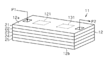
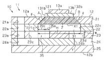
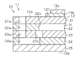
- the semiconductor device 10 shown in FIG. 1 includes a metal plate 13b on which a semiconductor element 13a is mounted and a metal plate 14b on which a semiconductor element 14a is mounted on one surface (first surface) 12a of a base 12 of a heat dissipation device 11. It is configured by being mounted.
- the metal plates 13b and 14b function as a wiring layer and a bonding layer, and are made of pure aluminum (for example, 1000 series aluminum which is industrial pure aluminum) or copper.
- IGBTs Insulated Gate Bipolar Transistors
- diodes are used as the semiconductor elements 13a and 14a.
- the semiconductor elements 13a and 14a and the metal plates 13b and 14b are joined by metal joining, for example, soldering or brazing. Further, the metal plates 13b and 14b and the heat dissipation device 11 are joined by metal joining, for example, soldering or brazing. Thereby, the metal plates 13 b and 14 b are mounted on the first surface 12 a of the base 12.
- the portion on which the metal plates 13b and 14b are placed (the portion indicated by the broken line in FIG. 2) is a mounting portion on which the metal plates 13b and 14b are mounted.
- the base 12 is configured by laminating a plurality of ceramic sheets (five in the first embodiment), and the heat dissipation device 11 is formed by firing the base 12.
- the ceramic material aluminum oxide, silicon nitride, silicon carbide, aluminum nitride, alumina / zirconium, or the like is used.
- a water cooling system is employ
- a material with high water resistance is preferable as a ceramic material.
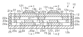
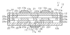
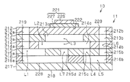
- the heat radiating device 11 of the first embodiment includes first to fifth ceramic sheets 21, 22, 23, 24, 25 as ceramic sheets.
- the first ceramic sheet 21 is described as “upper” and the fifth ceramic sheet 25 is described as “lower” in the heat dissipation device 11.
- the first ceramic sheet 21 constitutes the top plate portion of the heat dissipation device 11, and one surface (upper surface) thereof is the first surface 12 a of the base 12.
- the first ceramic sheet 21 is formed with a through-hole-shaped refrigerant supply hole 21a and a refrigerant discharge hole 21b.
- the refrigerant supply hole 21a and the refrigerant discharge hole 21b have the same opening area.
- a supply pipe P1 shown in FIGS.
- a discharge pipe P2 (shown in FIGS. 1 and 2) for discharging to the outside is connected.
- the second ceramic sheet 22 has a first coolant inflow hole 22a having a through hole shape.
- the first refrigerant inflow hole 22a is formed at a position overlapping the refrigerant supply hole 21a when viewed from the stacking direction of the first to fifth ceramic sheets 21, 22, 23, 24, 25.
- the second ceramic sheet 22 is formed with a first coolant outflow hole 22b having a through hole shape.
- the first refrigerant outflow hole 22b is substantially the same as the refrigerant discharge hole 21b when viewed from the stacking direction of the first to fifth ceramic sheets 21, 22, 23, 24, 25 (hereinafter sometimes simply referred to as the stacking direction A). It is formed at the overlapping position.
- the first refrigerant inflow hole 22a and the first refrigerant outflow hole 22b are formed at symmetrical positions.
- the first refrigerant inflow hole 22a and the first refrigerant outflow hole 22b have the same opening area.
- first slits 22 c as slits are formed between the first refrigerant inflow hole 22 a and the first refrigerant outflow hole 22 b in the second ceramic sheet 22.
- Each first slit 22c penetrates the second ceramic sheet 22 and extends linearly from a position near the first refrigerant inflow hole 22a in the second ceramic sheet 22 to the central portion of the second ceramic sheet 22. .
- the lengths of the first slits 22c are the same, and the first slits 22c have the same opening area.
- the plurality of first slits 22c are disposed at least partially directly below the first mounting portion 121 (the metal plate 13b and the semiconductor element 13a). That is, when viewed from the stacking direction A, the first slit 22 c at least partially overlaps the first mounting portion 121.
- a plurality of second slits 22d as slits are formed between the first refrigerant inflow hole 22a and the first refrigerant outflow hole 22b in the second ceramic sheet 22.
- Each of the second slits 22 d penetrates the second ceramic sheet 22 and extends linearly from a position near the first refrigerant outflow hole 22 b in the second ceramic sheet 22 to the central portion of the second ceramic sheet 22. .
- the lengths of the second slits 22d are the same, and the second slits 22d have the same opening area.
- the plurality of second slits 22d are at least partially disposed directly below the second mounting portion 131 (the metal plate 14b and the semiconductor element 14a). That is, when viewed from the stacking direction A, the second slit 22d overlaps the second mounting portion 131 at least partially.
- the third ceramic sheet 23 is formed with a second coolant inflow hole 23a having a through hole shape.
- the second refrigerant inflow hole 23a is formed at a position overlapping the first refrigerant inflow hole 22a when viewed from the stacking direction A.
- the third ceramic sheet 23 is formed with a second coolant outflow hole 23b having a through hole shape.
- the second refrigerant outflow hole 23b is formed at a position overlapping the first refrigerant outflow hole 22b when viewed from the stacking direction A.
- the second refrigerant inflow hole 23a and the second refrigerant outflow hole 23b have the same opening area.
- the third ceramic sheet 23 is formed with a first communication hole 23c extending in a direction orthogonal to the extending direction of each first slit 22c.
- the first communication hole 23c partially overlaps one end portion that is an end portion of each first slit 22c near the first refrigerant inflow hole 22a. Therefore, each 1st slit 22c and the 1st communicating hole 23c are connecting.
- a second communication hole 23d extending in a direction orthogonal to the extending direction of each first slit 22c is located at a position closer to the second refrigerant outflow hole 23b than the first communication hole 23c in the third ceramic sheet 23. Is formed.
- each first slit 22c and the second communication hole 23d communicate with each other.
- the third ceramic sheet 23 is formed with a third communication hole 23e extending in a direction orthogonal to the extending direction of each second slit 22d.
- the third communication hole 23e partially overlaps one end that is the end of each second slit 22d near the first refrigerant inflow hole 22a. Therefore, each second slit 22d and the third communication hole 23e communicate with each other.
- a fourth communication hole 23f extending in a direction orthogonal to the extending direction of each second slit 22d is located at a position closer to the second refrigerant outflow hole 23b than the third communication hole 23e in the third ceramic sheet 23. Is formed.
- the fourth communication hole 23f When viewed from the stacking direction A, the fourth communication hole 23f partially overlaps the other end, which is the end near the first refrigerant outflow hole 22b in each second slit 22d. Therefore, each second slit 22d and the fourth communication hole 23f communicate with each other.
- a first through hole 24a, a second through hole 24b, and a third through hole 24c are formed.
- the first through hole 24a overlaps with a part of the second refrigerant inflow hole 23a and the first communication hole 23c when viewed from the stacking direction A, and communicates the second refrigerant inflow hole 23a and the first communication hole 23c.
- the second through hole 24b overlaps a part of the second communication hole 23d and a part of the third communication hole 23e when viewed from the stacking direction A, and connects the second communication hole 23d and the third communication hole 23e. Communicate.
- the fifth ceramic sheet 25 constitutes a bottom plate portion of the heat dissipation device 11, and one surface (lower surface) thereof is the second surface 12 b of the base 12. That is, the second surface 12b is a surface located on the opposite side of the base 12 with respect to the first surface 12a.
- a fourth ceramic sheet 24, a third ceramic sheet 23, a second ceramic sheet 22, and a first ceramic sheet 21 are sequentially laminated on a fifth ceramic sheet 25. It is formed by.
- a refrigerant flow path 15 through which the refrigerant flows is formed.
- the refrigerant supply hole 21 a and the refrigerant discharge hole 21 b are opened in the
- the second communication hole 23d, the second through hole 24b, and the third communication hole 23e are part of the refrigerant flow path 15 that is located between the first mounting part 121 and the second mounting part 131 when viewed from the stacking direction A. Is configured. Then, the second communication hole 23d, the second through hole 24b, and the third communication hole 23e extend in a direction from the first mounting portion 121 to the second surface 12b, in a part of the refrigerant flow path 15, and further, A part of the refrigerant flow path 15 extending in the direction from the second surface 12b toward the second mounting portion 131 is formed.
- the second ceramic sheet 22 corresponds to a slit forming layer having a plurality of first slits 22c and second slits 22d constituting a part of the refrigerant flow path 15.
- the first communication hole 23c corresponds to a communication path in which a part of each first slit 22c near the first refrigerant inflow hole 22a overlaps and communicates with each first slit 22c.
- the second communication hole 23d corresponds to a communication path in which a part of each first slit 22c near the second refrigerant outflow hole 23b overlaps and communicates with the first slit 22c.
- the third communication hole 23e corresponds to a communication path in which a part of each second slit 22d near the first refrigerant inflow hole 22a overlaps and communicates with each second slit 22d.
- the fourth communication hole 23f corresponds to a communication path in which a part of each second slit 22d near the first refrigerant outflow hole 22b overlaps and communicates with each second slit 22d.
- the third ceramic sheet 23 corresponds to a communication path forming layer having a first communication hole 23c, a second communication hole 23d, a third communication hole 23e, and a fourth communication hole 23f corresponding to the communication path.
- the first slit 22c and the second slit 22d have the first mounting portion 121 and the second communication hole 23c, the second communication hole 23d, the third communication hole 23e, and the fourth communication hole 23f. 2 is located closer to the mounting portion 131.
- the second communication hole 23 d is continuously provided on the downstream side where the refrigerant flows in the first slit 22 c, and the second through hole 24 b is continuously provided to the second communication hole 23 d.
- An extended flow path W extending from the surface 12a toward the second surface 12b is formed.
- the second surface A part of the flow path surface Y1 of the flow path formed by the second through hole 24b located closer to 12b is opposed in the stacking direction of the first to fifth ceramic sheets 21 to 25.
- the flow path surface X1 is configured by the surface of the first ceramic sheet 21 positioned above the second ceramic sheet 22, and the flow path surface Y1 is the fifth ceramic sheet positioned below the fourth ceramic sheet 24. It consists of 25 faces. That is, the flow path formed by the first slit 22c is a flow path that constitutes the refrigerant flow path 15 positioned at the top in the stacking direction, and the flow path surface X1 corresponds to the upper surface of the flow path.
- the flow path formed by the second through holes 24b is a flow path that constitutes the refrigerant flow path 15 located at the bottom in the stacking direction, and the flow path surface Y1 corresponds to the lower surface of the flow path.
- the first fins 31 are formed between the adjacent first slits 22c.
- the second fins 32 are formed between the adjacent second slits 22d.
- the length H of the first fin 31 (the length of the first slit 22c) is the length included in the region Z (the region indicated by the dots in FIG. 6) when viewed from the stacking direction A. Is set.
- This region Z is a region sandwiched between the straight lines A and B in the cross section of the first ceramic sheet 21, and the straight lines A and B have an angle ⁇ of 45 ° with the first surface 12 a of the base 12. And a straight line extending from both ends 131b and 132b of the metal plate 13b.
- the angle ⁇ of the straight lines A and B with respect to the first surface 12a of the base 12 may be in the range of 30 ° to 60 °.
- a region Z sandwiched between the straight lines A and B indicates a heat transfer region in which heat generated from the semiconductor element 13a is transmitted to the heat dissipation device 11 via the metal plate 13b.
- the portion of the first communication hole 23c corresponding to the region Z is an overlapping portion 35 of each first slit 22c and the first communication hole 23c. . Therefore, the overlapping portion 35 is located in a heat transfer region where heat generated from the semiconductor element 13a is transmitted to the heat dissipation device 11 through the metal plate 13b. That is, when viewed from the stacking direction A, the overlapping portion 35 is located in the vicinity of the region where the first mounting portion 121 is provided. The overlapping portion 35 is located inside the first slit 22c with respect to the end 221c of each first slit 22c near the first refrigerant inflow hole 22a.
- the length of the second fin 32 (the length of the second slit 22d) and the explanation of the overlapping portion 36 between each second slit 22d and the third communication hole 23e, the length H of the first fin 31, And the description of the overlapping part 35 of each first slit 22c and the first communication hole 23c is the same, and the detailed description thereof is omitted.
- the overlapping portion 35 in the cross-sectional view of the heat dissipation device 11, includes a first overlapping portion 35 a directly below the first mounting portion 121 and a second overlapping portion 35 b other than the first overlapping portion 35 a. It is configured.
- the length of the second overlapping portion 35b is longer than the length of the first overlapping portion 35a.
- the length of the 2nd overlap part 35b said here is longer than the length of the 1st overlap part 35a means that the 2nd overlap part 35b is 1st refrigerant
- the 1st mounting part 121 was demonstrated here, you may set it as the same form also on the 2nd mounting part 131 side. Note that “directly below the mounting portion” is a region closer to the refrigerant flow path 15 with respect to the mounting portion, and corresponds to a region overlapping the mounting portion when viewed from the stacking direction A.
- the refrigerant supplied from the refrigerant supply source is supplied from the supply pipe P1 through the refrigerant supply hole 21a, the first refrigerant inflow hole 22a, the second refrigerant inflow hole 23a, the first through hole 24a, and the first communication hole 23c. It flows into the slit 22c.
- the refrigerant flows into the first slits 22c from the first communication holes 23c, the first slits from the first communication holes 23c are directed toward the first mounting portion 121 (the semiconductor element 13a and the metal plate 13b).
- the refrigerant is ejected into 22c.
- the metal plate The heat of the semiconductor element 13a transmitted to the heat dissipation device 11 (each first fin 31) through 13b is efficiently radiated by the refrigerant flowing through each first slit 22c, and the cooling performance for the semiconductor element 13a is improved.
- the semiconductor element 13a corresponds to a first object to be cooled.
- each first slit 22c flows into each second slit 22d through the second communication hole 23d, the second through hole 24b, and the third communication hole 23e.
- the second slits from the third communication holes 23e are directed toward the second mounting portion 131 (the semiconductor element 14a and the metal plate 14b).
- the refrigerant is jetted into 22d. Thereby, a jet flow is generated in the refrigerant flowing into the second slits 22d from the third communication holes 23e, and the refrigerant flowing in the second slits 22d is agitated.
- the metal plate The heat of the semiconductor element 14a transmitted to the heat dissipation device 11 (each second fin 32) via 14b is efficiently radiated by the refrigerant flowing through each second slit 22d, and the cooling performance for the semiconductor element 14a is improved.
- the semiconductor element 14a corresponds to a second object to be cooled.
- each second slit 22d radiates heat from the discharge pipe P2 via the fourth communication hole 23f, the third through hole 24c, the second refrigerant outflow hole 23b, the first refrigerant outflow hole 22b, and the refrigerant discharge hole 21b. It is discharged outside the device 11.
- the first slit 22c and the second slit 22d have the first mounting portion 121 and the second communication hole 23c, the second communication hole 23d, the third communication hole 23e, and the fourth communication hole 23f. It is located closer to the second mounting portion 131.
- the overlapping portion 35 between each first slit 22c and the first communication hole 23c and the overlapping portion 36 between each second slit 22d and the third communication hole 23e are the first mounting portion 121. And it is located in the vicinity of the area
- the flow of the refrigerant flowing into each first slit 22c from the first communication hole 23c and the flow of the refrigerant flowing into each second slit 22d from the third communication hole 23e are transferred to the first mounting portion 121 and the second mounting portion 131. It can be the flow going. Therefore, for example, the semiconductor elements 13a and 14a are efficiently cooled as compared with the case where the refrigerant flows through the first slits 22c and the second slits 22d along the first mounting part 121 and the second mounting part 131. Therefore, the cooling performance for the semiconductor elements 13a and 14a can be improved.
- the length of the second overlapping portion 35b is the first overlapping portion. It is longer than the length of the part 35a.
- a turbulent flow is generated after the refrigerant enters the refrigerant flow path of the narrow slit, but there is a time lag until the turbulent flow contributes to heat exchange. Therefore, since the length of the second overlapping portion 35b is longer than that of the first overlapping portion 35a, the semiconductor element 13a can be efficiently cooled by the refrigerant from the heat transfer region located on the upstream side. be able to.
- the cooling performance with respect to the semiconductor element 13a can be improved.
- the second mounting part 131 and the third mounting part 171 to be described later have the same configuration, so that when a plurality of semiconductor elements are mounted on each mounting part. The same effect can be obtained.
- a part of the refrigerant flow path 15 formed by the second communication hole 23d, the second through hole 24b, and the third communication hole 23e extends from the first mounting portion 121 to the second surface 12b. And extends in the direction toward the second mounting portion 131 from the second surface 12b. Therefore, the flow of the refrigerant flowing through the refrigerant flow path 15 can be a flow toward the first mounting portion 121 and the second mounting portion 131.
- the semiconductor element 13a , 14a can be efficiently cooled, and the cooling performance for the semiconductor elements 13a, 14a can be improved.
- the first communication hole 23c and the first slit 22c, and the second communication hole 23e and the second slit 22d are stepped toward the mounting portions.
- the refrigerant can be jetted in the step-like refrigerant flow path 15 and turbulent flow can be generated, and the flow path surfaces of the upstream end 221c of each first slit 22c and the upstream end of each second slit 22d. Cooling can be efficiently performed from X1, and cooling performance can be improved. As a result, it is not necessary to lengthen the flow path in order to improve the cooling performance, and the heat dissipation device 11 can be downsized.
- the refrigerant supply hole 21a and the refrigerant discharge hole 21b are opened in the first surface 12a of the base 12. Therefore, since the supply pipe P1 for supplying refrigerant and the discharge pipe P2 for discharging refrigerant can be connected to the first surface 12a of the base body 12, the components necessary for the heat dissipation device 11 are on the first surface 12a side of the base body 12. Can be arranged in a centralized manner. As a result, the heat dissipation device 11 can be reduced in size.
- the length H of the first fin 31 (the length of the first slit 22c) is set to a length included in the region Z when viewed from the stacking direction A.
- This region Z is a region which is sandwiched between straight lines A and B extending from both ends 131b and 132b of the metal plate 13b and having an angle ⁇ of 45 ° with the first surface 12a of the base 12. According to this, the length H of the first fin 31 can be a minimum length necessary for heat dissipation of the semiconductor element 13a.
- the length of the first slit 22c can be shortened as much as possible, and the inside of the first slit 22c can be compared with the case where the first slit 22c is formed to extend to a position that protrudes outward from the region Z. Pressure loss of the flowing refrigerant can be suppressed.
- the extended flow path W is a flow path in which the flow path surfaces X1 and Y1 face each other in the stacking direction, a portion where the flow path area is reduced can be reduced. Therefore, the pressure loss of the refrigerant can be reduced. Moreover, the extended flow path W becomes close to a linear flow path in the stacking direction A because the flow path surfaces X1 and Y1 face each other. For this reason, by reducing the stepped portion in the extended flow path W, the lateral expansion of the refrigerant flow path 15 can be reduced, and the size of the heat dissipation device 11 can be reduced.
- the first embodiment may be modified as follows.
- the second ceramic sheet 22 may be formed with a communication portion 22 h that communicates each first slit 22 c and each second slit 22 d.
- the 2nd communicating hole 23d, the 2nd through-hole 24b, and the 3rd communicating hole 23e may be deleted. According to this, only the second ceramic sheet 22 allows the refrigerant to flow from the first slits 22c to the second slits 22d via the communication portions 22h.
- the flow of the refrigerant becomes smoother.
- the pressure loss of the refrigerant can be suppressed.
- a metal plate on which a semiconductor element that is most desirably cooled is mounted on the first mounting portion 121.
- the opening area of the first communication hole 23c is made smaller than the opening area of the first communication hole 23c of the first embodiment, and the refrigerant passes through the first communication hole 23c.
- the flow rate may be increased. According to this, it becomes easy to produce a jet in the refrigerant
- the opening area of the third communication hole 23e is made smaller than the opening area of the third communication hole 23e of the first embodiment, so that the flow rate of the refrigerant when passing through the third communication hole 23e is increased. May be.
- the opening area of the first through hole 24a may be larger than the opening area of the first through hole 24a of the first embodiment.
- the opening area of the second through hole 24b may be larger than the opening area of the second through hole 24b of the first embodiment.
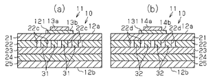
- a third mounting portion 171 as a mounting portion may be further provided at a portion of the second surface 12b located at the tip extending in the direction toward the second surface 12b.
- the second through holes 24b are replaced with the plurality of slits 41, and the plurality of fins 42 are disposed at portions partially overlapping the third mounting portion 171 in the fourth ceramic sheet 24 when viewed from the stacking direction A. Is formed. Then, the metal plate 17b on which the semiconductor element 17a is mounted is mounted on the third mounting portion 171.
- the semiconductor element 17a is cooled by being dissipated by the refrigerant flowing through the plurality of slits 41.
- the semiconductor element 17a corresponds to a third cooling object. According to this, as many semiconductor elements as possible can be mounted on the heat dissipation device 11, the entire volume can be reduced, and the cooling performance of the semiconductor elements 13 a, 14 a, and 17 a mounted on the heat dissipation device 11 can be improved. .
- the second ceramic sheet may have a plurality of wavy first slits 43 and second slits 44 as shown in FIG. According to this, compared with the first slit 22c and the second slit 22d that are linear in plan view, the heat radiating surface area is increased, and the cooling performance for the semiconductor elements 13a and 14a can be further improved by having a refrigerant stirring effect. .
- the positions of the refrigerant supply hole and the refrigerant discharge hole of the refrigerant flow path 15 may be changed.
- the coolant supply hole and the coolant discharge hole may be opened on the second surface 12 b of the base 12.
- the first slit 22c and the second slit 22d are at least partially overlapped with the region including the first mounting portion 121 and the second mounting portion 131 when viewed from the stacking direction A. That's fine.
- the number of the first slits 22c and the second slits 22d may be changed.
- the number of slits is changed depending on the area of the semiconductor element, the passage width of the coolant channel 15 and the like. For example, if the area area for forming the refrigerant flow path 15 is the same, the number of slits decreases when the passage width is increased, and the number of slits increases when the passage width is reduced.
- the number of laminated ceramic sheets constituting the base 12 of the heat dissipation device 11 may be changed.
- the number of laminated ceramic sheets is increased or decreased according to the cross-sectional area (flow path area) of the refrigerant flow path 15 formed in the heat dissipation device 11.
- the numbers of semiconductor elements and metal plates are not particularly limited. In the first embodiment, the number of mounting portions is not particularly limited.
- the cooling method of the heat dissipation device 11 may be air cooling.
- a cooling gas such as air flows through the refrigerant flow path 15.
- the extended flow path having the same configuration as the extended flow path W is the second slit 22d. It may be provided on the side.
- linear extended flow paths W1 and W2 extending in the stacking direction of the first to fifth ceramic sheets 21 to 25 may be provided.
- the extended flow path W1 is a partial flow path of the refrigerant flow path 15 configured by the first slit 22c, the second communication hole 23d, and the second through hole 24b.
- the extended flow path W2 is a partial flow path of the refrigerant flow path 15, and includes a second slit 22d, a fourth communication hole 23f, and a third through hole 24c. As shown in FIG.
- the flow path surface X1 formed by the surface of the first ceramic sheet 21 and the flow path surface Y1 formed by the surface of the fifth ceramic sheet 25 face each other in the stacking direction. To do. This is the same for the extended flow path W2.
- the pressure loss of the refrigerant can be further reduced as compared with the case where the flow paths are formed in a stepped shape. Further, by reducing the stepped portion, the lateral expansion of the refrigerant flow path 15 can be further reduced, and the physique of the heat dissipation device 11 can be further reduced.
- the position of the end of the fourth communication hole 23f near the second refrigerant outflow hole 23b and the end of the second slit 22d near the first refrigerant outflow hole 22b are arranged. Match the position. Further, when forming the extended flow path W2, the position of the end opposite to the end near the second refrigerant outflow hole 23b (the end close to the second cooling inflow hole 23a) in the fourth communication hole 23f, The position of the end of the third through hole 24c near the second through hole 24b is matched.
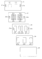
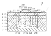
- the heat radiating device 11 includes a base 218 formed by laminating a plurality (six in the second embodiment) of first to sixth ceramic members 212, 213, 214, 215, 216, and 217.
- the material of the ceramic member aluminum oxide, silicon nitride, silicon carbide, aluminum nitride, alumina / zirconia, or the like is used. Further, when the water cooling method is adopted as the cooling method of the heat dissipation device 11, a material having high water resistance is preferable as the ceramic material.
- the base 218 has a refrigerant supply hole 219 and a refrigerant discharge hole 220.
- the externally supplied refrigerant is supplied to the refrigerant flow path formed inside the base body 218 through the refrigerant supply hole 219, and the refrigerant flowing through the refrigerant flow path is discharged to the outside of the base body 218 through the refrigerant discharge hole 220. Is done.
- the refrigerant supply hole 219 and the refrigerant discharge hole 220 open to the first ceramic member 212 that is a component of the base 218. That is, the refrigerant supply hole 219 and the refrigerant discharge hole 220 are opened on one surface (first surface) of the base 218, respectively.
- a supply pipe P1 connected to an external refrigerant supply source can be connected to the refrigerant supply hole 219, and a discharge pipe P2 for discharging the refrigerant to the outside can be connected to the refrigerant discharge hole 220.
- the base 218 has the coolant channel as viewed from the stacking direction of the first to sixth ceramic members 212, 213, 214, 215, 216, and 217 (hereinafter sometimes simply referred to as the stacking direction B).
- a mounting portion 222 (shown by a broken line in FIG. 16) of the electronic component 221 is provided at a position at least partially overlapping with the electronic component 221. In the second embodiment, the mounting portion 222 is provided on the surface (first surface) of the first ceramic member 212 where the coolant supply hole 219 and the coolant discharge hole 220 are opened, and is located on the surface outside the base body 218.
- the semiconductor device 10 is a metal plate in which a semiconductor element 226 is mounted as an electronic component 221 on a mounting portion 222 provided on a base 218 of the heat dissipation device 11, as in the first embodiment described above. 227 is mounted.
- the metal plate 227 functions as a wiring layer and a bonding layer, and is pure aluminum (for example, 1000 series aluminum which is industrial pure aluminum) or copper.
- the semiconductor element 226 is, for example, an IGBT (Insulated Gate Bipolar Transistor) or a diode.
- the semiconductor element 226 and the metal plate 227, and the metal plate 227 and the heat dissipation device 11 are metal-bonded by, for example, soldering or brazing.
- a coolant channel 228 communicating with the coolant supply hole 219 and the coolant discharge hole 220 is formed inside the base 218 of the heat dissipation device 11.
- the first ceramic member 212 that is a component of the base 218 and has the mounting portion 222 is referred to as “upper”
- the sixth ceramic member 217 that is farthest from the first ceramic member 212 is referred to as “ This will be described as “below”.
- the refrigerant flow path 228 includes first to seventh flow paths L1 to L7.
- the first flow path L1 is a linear flow path that is connected to the coolant supply hole 219 and flows the coolant downward in the vertical direction.
- the second flow path L2 is a flow path branched from the first flow path L1 and flowing the refrigerant obliquely upward.
- the third flow path L3 is a linear flow path that is connected to the second flow path L2 and is formed immediately below the mounting portion 222, and allows the refrigerant to flow in the horizontal direction.
- the fourth flow path L4 is a linear flow path that is connected to the third flow path L3 and allows the refrigerant to flow downward in the vertical direction.
- the fifth flow path L5 is a linear flow path that is connected to the fourth flow path L4 and allows the refrigerant to flow in the horizontal direction.
- the sixth flow path L6 is a linear flow path that is connected to the fifth flow path L5 and allows the refrigerant to flow upward in the vertical direction.
- the seventh flow path L7 is branched from the first flow path L1 together with the second flow path L2, and the straight line flows the refrigerant from the lower side in the vertical direction toward the third flow path L3 located immediately below the mounting portion 222. It is a channel.
- the first to sixth ceramic members 212 to 217 are formed with a plurality of flow path holes that are components of the refrigerant flow path 228.
- the first to seventh flow paths L1 to L7 are configured by connecting a plurality of flow path holes in the stacking direction of the first to sixth ceramic members 212 to 217.
- each member of the heat dissipation device 11 will be described with reference to FIG.
- the sheet forming the ceramic member is referred to as a ceramic sheet and will be described using the same reference numerals as the ceramic member.
- the six first to sixth ceramic sheets 212 to 217 which are constituent elements of the heat dissipation device 11 are rectangular sheets having the same length and width. is there.
- the first ceramic sheet 212 forms a top plate of the heat radiating device 11 provided with the mounting portion 222.
- a first flow path hole 212 a having a refrigerant supply hole 219 and a refrigerant discharge hole 220.
- a sixth passage hole 212b On both sides of the mounting portion 222, a first flow path hole 212 a having a refrigerant supply hole 219 and a refrigerant discharge hole 220.
- a sixth passage hole 212b On both sides of the mounting portion 222.
- the first channel hole 212a and the sixth channel hole 212b have the same opening area.
- the second ceramic sheet 213 is positioned below the first ceramic sheet 212 in the stacked state.
- the second ceramic sheet 213 has a first flow path hole 213a and a sixth flow path hole 213b.
- the first channel hole 213a is formed at the same position as the first channel hole 212a of the first ceramic sheet 212, communicates with the first channel hole 212a, and the first channel hole 212a. Have the same opening area.
- the sixth flow path hole 213b is formed at the same position as the sixth flow path hole 212b of the first ceramic sheet 212, communicates with the sixth flow path hole 212b, and the sixth flow path hole 212b. Have the same opening area.
- the second ceramic sheet 213 has a plurality of slit-shaped third flow passage holes 213c (5 in the second embodiment) between the first flow passage holes 213a and the sixth flow passage holes 213b. Book).
- Each third channel hole 213c has the same shape and extends linearly.
- the length along the extending direction (length direction) is longer than the length along the same direction in the mounting portion 222, and the plurality of third channel holes 213c are These are positioned at equal intervals along a direction orthogonal to the extending direction (length direction).
- the third flow path hole 213c is partially located directly below the mounting portion 222, and the other third flow path holes 213c are stacked. When viewed from the direction B, the mounting portion 222 is located outside.
- the third ceramic sheet 214 is positioned below the second ceramic sheet 213 in the stacked state.
- the third ceramic sheet 214 has a first flow path hole 214a and a sixth flow path hole 214b.
- the first channel hole 214a is formed at the same position as the first channel hole 213a of the second ceramic sheet 213, communicates with the first channel hole 213a, and the first channel hole 213a. Have the same opening area.
- the sixth channel hole 214b communicates with the sixth channel hole 213b of the second ceramic sheet 213 and has the same opening area as the sixth channel hole 213b.
- the third ceramic sheet 214 has a plurality of slit-like third flow passage holes 214c (5 in the second embodiment) between the first flow passage holes 214a and the sixth flow passage holes 214b. Book).
- Each of the third flow path holes 214c has the same shape and extends linearly.
- Each third flow path hole 214c is located at a position partially overlapping with the third flow path hole 213c of the second ceramic sheet 213 when viewed from the stacking direction B.
- the length along the extending direction is longer than the length along the same direction in the third channel hole 213c of the second ceramic sheet 213. .
- the plurality of third flow path holes 214c are located at equal intervals along a direction orthogonal to the extending direction (length direction). In addition, in a state where the second ceramic sheet 213 and the third ceramic sheet 214 are laminated, both ends of the third flow path hole 214c are positions of both ends of the third flow path hole 213c when viewed from the stacking direction B. From the outside to the outside and projecting the same length.
- the fourth ceramic sheet 215 is positioned below the third ceramic sheet 214 in the stacked state.
- the fourth ceramic sheet 215 has a first passage hole 215a.
- the first flow path hole 215a overlaps the entire range of the first flow path hole 214a when viewed from the stacking direction B in a state where the third ceramic sheets 214 are stacked, and the third flow path hole 214c.
- the opening area of the first flow path hole 215 a is larger than the opening area of the first flow path hole 214 a of the third ceramic sheet 214.
- the length along the direction orthogonal to the extending direction of the third channel hole 214c of the third ceramic sheet 214 is the third channel hole located at the outermost position. It is the same as the length between the inner surfaces of 214c.
- the fourth ceramic sheet 215 has a sixth passage hole 215b, and the sixth passage hole 215b is formed at the same position as the sixth passage hole 214b of the third ceramic sheet 214.
- the sixth channel hole 214b communicates with and has the same opening area as the sixth channel hole 214b.
- the fourth ceramic sheet 215 has a fourth channel hole 215c between the first channel hole 215a and the sixth channel hole 215b, and the fourth channel hole 215c is laminated. When viewed from the direction B, each third channel hole 214c overlaps with a part of the range near the sixth channel hole 214b.
- the fourth ceramic sheet 215 includes a plurality of slit-like seventh flow passage holes 215d (five in the second embodiment) between the first flow passage holes 215a and the fourth flow passage holes 215c. )
- Each of the seventh flow path holes 215d has the same shape and extends linearly.
- Each of the seventh flow path holes 215d is located at a position overlapping the third flow path holes 214c of the third ceramic sheet 214 when viewed from the stacking direction B.
- the length along the extending direction is the same in each of the third flow path holes 213c and 214c of the second and third ceramic sheets 213 and 214. Shorter than each length along the direction.
- the plurality of seventh passage holes 215d are located at equal intervals along a direction orthogonal to the extending direction (length direction).
- the center of each of the seventh flow path holes 215d is located on a line passing through the center of the mounting portion 222 in a direction orthogonal to the direction in which the third flow path holes 213c and 214c extend.
- the fifth ceramic sheet 216 is positioned below the fourth ceramic sheet 215 in the stacked state.
- the fifth ceramic sheet 216 has a first flow path hole 216a and a fifth flow path hole 216b.
- the first flow path holes 216a are viewed in the stacking direction B with the fourth ceramic sheets 215 being stacked, and the entire first flow path holes 215a and all of the seventh flow path holes 215d. It is in a position that overlaps the range.
- the fifth channel hole 216b is formed in a state where the fourth ceramic sheet 215 is stacked, and the entire range of the sixth channel hole 215b and the fourth channel hole 215c are viewed from the stacking direction B. It is in a position that overlaps the entire range.
- the sixth ceramic sheet 217 is positioned below the fifth ceramic sheet 216 in a stacked state.
- the sixth ceramic sheet 217 constitutes a bottom plate of the heat dissipation device 11.
- the base 218 of the heat dissipation device 11 is laminated on the sixth ceramic member 217 in the order of the fifth ceramic member 216, the fourth ceramic member 215, the third ceramic member 214, the second ceramic member 213, and the first ceramic member 212. Consists of.
- the coolant channel 228 is formed inside the base body 218 as described above.
- the first flow path L1 is formed by connecting the first flow path holes 212a, 213a, 214a, 215a, 216a of the first to fifth ceramic members 212-216.
- the second flow path L2 includes a partial range of the first flow path hole 215a of the fourth ceramic member 215, a partial range of the third flow path hole 214c of the third ceramic member 214, and the second ceramic.
- a part of the third channel hole 213c of the member 213 is connected in a stepped manner.
- the third flow path L3 is formed by connecting the third flow path hole 213c of the second ceramic member 213 and the third flow path hole 214c of the third ceramic member 214.
- the fourth flow path L4 includes a part of the third flow path hole 214c of the third ceramic member 214, the fourth flow path hole 215c of the fourth ceramic member 215, and the fifth of the fifth ceramic member 216. It is formed by connecting a part of the channel hole 216b in a straight line.
- the fifth flow path L5 is formed by the fifth flow path hole 216b of the fifth ceramic member 216 connected to the fourth flow path hole 215c of the fourth ceramic member 215.
- the sixth flow path L6 is connected to the fifth flow path hole 216b of the fifth ceramic member 216, and the sixth flow path holes 212b, 213b, 214b, and 215b of the first to fourth ceramic members 212 to 215 are connected. It is formed by connecting.
- the seventh flow path L7 is formed by a seventh flow path hole 215d of the fourth ceramic member 215 connected to the first flow path hole 216a of the fifth ceramic member 216.
- the third flow path L3 is a direct flow path through which the refrigerant flows just below the mounting portion 222.
- the second flow path L2 communicates with the upstream side in the direction of refrigerant flow in the third flow path L3, and the refrigerant flows together with the first flow path L1 connected to the second flow path L2.
- the supply flow path to supply to In the second embodiment, the fourth flow path L4 communicates with the downstream side in the direction of refrigerant flow in the third flow path L3, and is connected to the fifth flow path L5 and the fifth flow path L5.
- a discharge flow path for discharging the refrigerant that has flowed through the third flow path L3 together with the connected sixth flow path L6 is configured.
- the seventh flow path L7 is located between the supply flow path and the discharge flow path, and ejects the third flow path L3 from the lower side to the upper side in the vertical direction. It becomes a flow path.
- the seventh flow path L7 serving as the ejection flow path ejects the refrigerant toward the center of the mounting portion 222.
- the base 218 has fins 230 formed between the third flow path holes 213 c of the second ceramic member 213 constituting the third flow path L 3, and the third flow path.
- Fins 231 are formed between the third flow path holes 214c of the third ceramic member 214 constituting L3.
- the fins 230 and 231 overlap in the stacking direction B. These fins 230 and 31 are straight fins.
- the refrigerant that has flowed into the refrigerant flow path 228 via the refrigerant supply hole 219 once flows below the heat dissipation apparatus 11 through the first flow path L1.
- the refrigerant that has flowed through the first flow path L1 is divided into the second flow path L2 and the seventh flow path L7 that branch from the first flow path L1, flows through the respective flow paths, and the second flow path L2 and the second flow path L7. It flows from the seventh flow path L7 to the third flow path L3.
- the heat of the electronic component 221 (semiconductor element 226 and metal plate 227) is radiated to the refrigerant flowing through the third flow path L3 through the surface of the first ceramic member 212 and the fins 230 and 231 that block the third flow path L3. Then, the heat-exchanged refrigerant flowing through the third flow path L3 flows through the fourth flow path L4, the fifth flow path L5, and the sixth flow path L6, and is discharged to the outside through the refrigerant discharge hole 220.
- the second flow path L2 that causes the coolant to flow from the outer peripheral area of the mounting part 222 of the electronic component 221 toward the mounting part 222 from the oblique direction with respect to the third flow path L3, and the mounting part And a seventh flow path L7 through which the refrigerant flows from the bottom toward the top toward the center of 222.
- the refrigerant flowing through the second flow path L2 and the seventh flow path L7 is ejected from the bottom toward the third flow path L3. Thereby, a jet flow is generated in the refrigerant flowing through the third flow path L3, and the refrigerant is agitated.
- the temperature boundary layer of the refrigerant flowing through the third flow path L3 is thinned.
- the seventh flow path L7 allows the coolant to be directly applied to the heat generating surface by ejecting the coolant toward the central portion of the electronic component 221 having the highest temperature in the mounting portion 222. Effectively thin.
- the refrigerant can be directly applied toward the mounting portion 222.
- the refrigerant flowing through the third flow path L3 can be effectively stirred, and the temperature boundary layer of the refrigerant flowing through the third flow path L3 can be thinned. Therefore, the cooling performance with respect to the cooling object can be improved.
- the seventh flow path L7 is formed as a flow path branched from the first flow path L1. For this reason, the structure of the refrigerant
- the refrigerant supply hole 219 and the refrigerant discharge hole 220 are opened on the surface (first surface) of the base body 218 provided with the mounting portion 222. For this reason, components necessary for the heat radiating device 11 such as the supply pipe P1 connected to the refrigerant supply hole 219 and the discharge pipe P2 connected to the refrigerant discharge hole 220 can be collectively arranged. As a result, the heat dissipation device 11 can be reduced in size.
- a linear fourth flow path L4 is provided. For this reason, the pressure loss of a refrigerant
- the fourth flow path L4 as a straight flow path, a stepped portion in the refrigerant flow path 228 can be reduced, and the spread of the refrigerant flow path 228 in the lateral direction can be reduced. . Therefore, the heat dissipation device 11 can be reduced in size.
- the electronic component 221 (the semiconductor element 226 and the metal plate 227) can be efficiently cooled, and the cooling performance for the electronic component 221 can be improved.
- the heat dissipating device 11 itself can have a cooling function and an insulating function. Therefore, the semiconductor device 10 can be configured by directly joining the electronic component 221 (the semiconductor element 226 and the metal plate 227) to the heat dissipation device 11. Therefore, the number of parts in the semiconductor device 10 can be reduced and the size can be reduced.
- a plurality of seventh flow paths L7 may be formed in the refrigerant flow path 228.
- these seventh flow paths L7 are positioned in the region of the mounting portion 222 when viewed from the stacking direction B, so that the effect of the jet flow is further improved. It can be demonstrated.
- at least one seventh flow path L7 among the plurality of seventh flow paths L7 may be provided at a position where the refrigerant is ejected toward the central portion of the mounting portion 222.
- the plurality of seventh flow paths L7 can directly apply the refrigerant to the mounting portion 222 from a wide range, and the temperature boundary layer of the refrigerant flowing through the third flow path L3 can be effectively thinned. . Therefore, the cooling performance with respect to the cooling object can be further improved.
- the base 218 may be formed with corrugated fins by corrugating the third flow passage holes 213c and 214c.
- the wavy fin has an increased contact area with the refrigerant and has an effect of stirring the refrigerant, so that the cooling performance can be improved.
- the flow path for supplying the refrigerant to the second flow path L2 and the flow path for supplying the refrigerant to the seventh flow path L7 may be different.
- the refrigerant may be directly supplied from the outside to the seventh flow path L7.
- the positions of the refrigerant supply hole 219 and the refrigerant discharge hole 220 in the base 218 may be changed.
- the refrigerant supply hole 219 and the refrigerant discharge hole 220 may be arranged in the sixth ceramic member 217, or one of them may be arranged in the first ceramic member 212 and the other may be arranged in the sixth ceramic member 217. good.
- the fourth flow path L4 may be a flow path extending obliquely downward by connecting a part of the flow path hole 216b in a stepped manner.
- the number of the third channel holes 213c and 214c may be changed. These numbers are changed depending on the area of the semiconductor element, the passage width of the coolant channel 228, and the like. For example, if the area of the refrigerant flow path 228 is the same, the number decreases when the passage width is increased, and the number increases when the passage width is decreased.
- the number of laminated ceramic members constituting the base 218 of the heat dissipation device 11 may be changed.
- the number of laminated ceramic members is increased or decreased according to the cross-sectional area (flow path area) of the refrigerant flow path 228 formed in the heat dissipation device 11.
- the cooling method of the heat dissipation device 11 may be either liquid cooling or air cooling.
- the number of electronic components 221 mounted on the heat dissipation device 11 may be changed.
- the refrigerant flow path 228 inside the base 218 is appropriately changed depending on the number and arrangement of the mounting portions 222 on which the electronic components 221 are mounted.
- SYMBOLS 10 Semiconductor device, 11 ... Radiation device, 12,218 ... Base
Abstract
Description
本開示の目的は、冷却対象物に対する冷却性能を向上させることができる放熱装置、及び半導体装置を提供することである。
以下、本発明を具体化した第1実施形態を図1~図6にしたがって説明する。
図1に示す半導体装置10は、放熱装置11の基体12における一方の面(第1面)12aに、半導体素子13aが実装された金属板13b、及び半導体素子14aが実装された金属板14bが搭載されることで、構成されている。金属板13b,14bは、配線層及び接合層として機能するとともに、純アルミニウム(例えば、工業用純アルミニウムである1000系アルミニウム)や銅により形成されている。また、半導体素子13a,14aとしては、例えばIGBT(Insulated Gate Bipolar Transistor)やダイオードが用いられる。また、半導体素子13a,14aと金属板13b,14bとは、金属接合、例えば、半田付けやろう付けによって接合されている。また、金属板13b,14bと放熱装置11とは、金属接合、例えば、半田付けやろう付けによって接合されている。これにより、金属板13b,14bは、基体12における第1面12aに搭載されている。
冷媒供給源から供給された冷媒は、供給管P1から冷媒供給孔21a、第1冷媒流入孔22a、第2冷媒流入孔23a、第1貫通孔24a及び第1連通孔23cを介して各第1スリット22c内に流れ込む。ここで、第1連通孔23cから各第1スリット22cに冷媒が流れ込む際には、第1搭載部121(半導体素子13a及び金属板13b)に向かうように第1連通孔23cから各第1スリット22c内に冷媒が噴出される。これにより、第1連通孔23cから各第1スリット22cに流れ込む冷媒に噴流が生じ、各第1スリット22c内を流れる冷媒が撹拌される。その結果、例えば、冷媒が第1面12aに沿って流れた後、第1搭載部121(基体12における第1面12a)に沿うように各第1スリット22cを流れる場合に比べると、金属板13bを介して放熱装置11(各第1フィン31)に伝達される半導体素子13aの熱が、各第1スリット22cを流れる冷媒によって効率良く放熱され、半導体素子13aに対する冷却性能が向上する。なお、第1実施形態では、半導体素子13aは第1の冷却対象物に相当する。
(1)積層方向Aにおいて、第1スリット22c及び第2スリット22dは、第1連通孔23c、第2連通孔23d、第3連通孔23e及び第4連通孔23fに対し第1搭載部121及び第2搭載部131寄りに位置している。そして、積層方向Aから見て、各第1スリット22cと第1連通孔23cとの重なり部35、及び各第2スリット22dと第3連通孔23eとの重なり部36は、第1搭載部121及び第2搭載部131が設けられた領域の近傍に位置している。よって、第1連通孔23cから各第1スリット22cに流れ込む冷媒の流れ、及び第3連通孔23eから各第2スリット22dに流れ込む冷媒の流れが、第1搭載部121及び第2搭載部131に向かう流れとされ得る。よって、例えば、冷媒が第1搭載部121及び第2搭載部131に沿うように各第1スリット22c及び各第2スリット22dを流れる場合に比べると、半導体素子13a,14aが効率良く冷却されることができ、半導体素子13a,14aに対する冷却性能が向上し得る。
図7に示すように、第2セラミックシート22に、各第1スリット22cと各第2スリット22dとを連通する連通部22hが形成されてもよい。そして、図8に示すように、第2連通孔23d、第2貫通孔24b及び第3連通孔23eが削除されてもよい。これによれば、第2セラミックシート22のみで、各第1スリット22cから連通部22hを介して各第2スリット22dに冷媒が流され得る。よって、各第1スリット22cから第2連通孔23d、第2貫通孔24b及び第3連通孔23eを介して各第2スリット22dに冷媒を流す場合に比べると、冷媒の流れがスムーズになるため、冷媒の圧力損失が抑制され得る。なお、この場合、第1搭載部121に、最も冷却されることが望ましい半導体素子を実装した金属板が搭載されるのが好ましい。
上記第1実施形態において、搭載部の数は特に限定されるものではない。
図4に示す第1実施形態の放熱装置11において、第1スリット22cに繋がる延設流路Wに加えて、その延設流路Wと同様の構成を有する延設流路が第2スリット22d側に設けられても良い。
以下、本発明を具体化した第2実施形態を図16~図20にしたがって説明する。
図16に示すように、放熱装置11は、複数枚(第2実施形態では6枚)の第1~第6セラミック部材212,213,214,215,216,217を積層してなる基体218を備えている。セラミック部材の材料としては、酸化アルミニウム、窒化珪素、炭化珪素、窒化アルミニウム、及びアルミナ・ジルコニアなどが用いられる。また、放熱装置11の冷却方式として水冷方式を採用する場合、セラミックの材料としては、耐水性の高い材料が好ましい。
図18及び図19に示すように、放熱装置11の基体218の内部には、冷媒供給孔219と冷媒排出孔220とに連通する冷媒流路228が形成されている。なお、以下の説明は、基体218の構成要素であるとともに搭載部222を有する第1セラミック部材212を「上」とし、第1セラミック部材212から最も離れた位置にある第6セラミック部材217を「下」として説明する。
第2実施形態の放熱装置11では、冷媒供給孔219を介して冷媒流路228に流入した冷媒が第1流路L1によって一旦、放熱装置11の下方に流れる。第1流路L1を流れた冷媒は、第1流路L1から分岐する第2流路L2と第7流路L7とに分流し、それぞれの流路を流れるとともに、第2流路L2及び第7流路L7から第3流路L3に流れる。第3流路L3を流れる冷媒には、第3流路L3を塞ぐ第1セラミック部材212の面及びフィン230,231を通じて電子部品221(半導体素子226と金属板227)の熱が放熱される。そして、第3流路L3を流れる熱交換後の冷媒は、第4流路L4、第5流路L5及び第6流路L6を流れ、冷媒排出孔220から外部に排出される。
(8)第3流路L3に対して鉛直方向下方から上方に向けて冷媒を噴出させる第7流路L7を設けることで、冷媒を搭載部222に向けて直接的に当てることができる。これにより、第3流路L3を流れる冷媒の攪拌を効果的に行うことができ、第3流路L3を流れる冷媒の温度境界層を薄くできる。したがって、冷却対象物に対する冷却性能を向上させることができる。
(10)第7流路L7は、冷媒を搭載部222の中央部に向かって噴出させる。これにより、第3流路L3を流れる冷媒の温度境界層を効果的に薄くできる。したがって、冷却対象物に対する冷却性能をさらに向上させることができる。
上記第2実施形態において、図21に示すように、冷媒流路228に複数の第7流路L7を形成しても良い。複数の第7流路L7を形成する場合、これらの第7流路L7は冷媒の噴出位置を、積層方向Bから見て、搭載部222の領域内に位置させることで、噴流の効果をより発揮させることができる。また、複数の第7流路L7のうち、少なくとも1つの第7流路L7を搭載部222の中央部に向けて冷媒を噴出させる位置に設けると良い。この構成によれば、複数の第7流路L7によって搭載部222に対して広範囲から冷媒を直接的に当てることができ、第3流路L3を流れる冷媒の温度境界層を効果的に薄くできる。したがって、冷却対象物に対する冷却性能をさらに向上させることができる。
上記第2実施形態において、放熱装置11に搭載する電子部品221の数を変更しても良い。なお、基体218内部の冷媒流路228は、電子部品221を搭載する搭載部222の数や配置などによって適宜変更される。
Claims (13)
- 放熱装置であって、
複数のセラミックシートが積層されてなる基体と、
該基体の内部に設けられた冷媒が流れる冷媒流路と、
冷却対象物が搭載される部位として前記基体の第1面に設けられた少なくとも一つの搭載部と、
前記複数のセラミックシートのうちの少なくとも一つによって形成されるスリット形成層であって、該スリット形成層は、前記冷媒流路の一部を構成する複数のスリットを有し、該複数のスリットは、前記セラミックシートの積層方向から見て、少なくとも部分的に前記搭載部を含む領域と重なり合うように形成された、前記スリット形成層と、
前記複数のセラミックシートのうちの少なくとも一つによって形成される連通路形成層であって、該連通路形成層は、前記冷媒流路の一部を構成するとともに前記複数のスリットに連通する連通路を有し、前記セラミックシートの積層方向において、前記スリットは、前記連通路に対し前記搭載部寄りに位置する、前記連通路形成層と、を有し、
前記積層方向から見て、前記スリットと前記連通路とにおける重なり部は、前記搭載部が設けられた領域の近傍に位置している、放熱装置。 - 断面視において、前記搭載部に対応する冷媒流路の上流側に位置する前記重なり部は、前記搭載部直下の第1の重なり部と、該第1の重なり部以外の第2の重なり部とを含み、該第2の重なり部の長さが、前記第1の重なり部の長さよりも長くなっている、請求項1に記載の放熱装置。
- 前記基体の第1面には、複数の前記搭載部が並設されているとともに、
前記積層方向から見て、隣り合う搭載部の間に位置する前記冷媒流路の一部は、前記隣り合う搭載部の一方から、前記基体における前記第1面に対して反対側の第2面に向かう方向に延びるとともに、さらに、該第2面から前記隣り合う搭載部の他方に向かう方向に延びている、請求項1又は2に記載の放熱装置。 - 前記基体は、隣り合う搭載部の一方から前記第2面に向かう方向に前記冷媒流路の一部が延びた先に位置する前記第2面の部位に、別の冷却対象物が搭載される搭載部をさらに有している、請求項3に記載の放熱装置。
- 前記スリット形成層のスリットにおいて前記冷媒が流れる方向の下流側には、前記基体における前記第1面に対して反対側の第2面に向かって延びる延設流路が設けられており、
前記第1面寄りに位置する前記延設流路の流路面の一部と前記第2面寄りに位置する前記延設流路の流路面の一部とが前記積層方向において対向している、請求項1~4のいずれか一項に記載の放熱装置。 - 前記スリット形成層は、複数の第1スリット、複数の第2スリット、及び、これら複数の第1スリットと複数の第2スリットとを連通する連通部、を有しており、
前記複数の第1スリットは、前記積層方向から見て、隣り合う搭載部の一方を含む領域と少なくとも部分的に重なり合っており、
前記複数の第2スリットは、前記積層方向から見て、隣り合う搭載部の他方を含む領域と少なくとも部分的に重なり合っている、請求項3に記載の放熱装置。 - 前記冷媒流路は、
前記搭載部の直下に形成された直下流路と、
前記直下流路における冷媒の流れる方向の上流側に連通されるとともに冷媒を前記直下流路に供給する供給流路と、
前記直下流路における冷媒の流れる方向の下流側に連通されるとともに前記直下流路を流れた冷媒を排出する排出流路と、
前記供給流路と前記排出流路との間に位置し、前記直下流路に対して鉛直方向下方から上方に向けて冷媒を噴出させる噴出流路と、を有する、請求項1に記載の放熱装置。 - 前記噴出流路は、前記供給流路から分岐している、請求項7に記載の放熱装置。
- 複数の前記噴出流路を有する、請求項7又は8に記載の放熱装置。
- 前記噴出流路は、前記搭載部の中央部に向けて前記冷媒を噴出させる、請求項7~9のいずれか一項に記載の放熱装置。
- 放熱装置であって、
複数のセラミック部材が積層されてなる基体と、
前記基体の内部に設けられた冷媒流路と、
冷却対象物が搭載される部位として前記基体の第1面に設けられた少なくとも一つの搭載部とを備え、
前記冷媒流路は、
前記搭載部の直下に形成された直下流路と、
前記直下流路における冷媒の流れる方向の上流側に連通されるとともに冷媒を前記直下流路に供給する供給流路と、
前記直下流路における冷媒の流れる方向の下流側に連通されるとともに前記直下流路を流れた冷媒を排出する排出流路と、
前記供給流路と前記排出流路との間に位置し、前記直下流路に対して鉛直方向下方から上方に向けて冷媒を噴出させる噴出流路と、を有する、放熱装置。 - 前記冷媒流路は、前記基体における前記第1面に開口した冷媒供給孔及び冷媒排出孔を備える、請求項1~11のいずれか一項に記載の放熱装置。
- 請求項1~12のいずれか一項に記載の放熱装置と、
前記放熱装置の前記搭載部に搭載される金属板と、
前記金属板に実装される半導体素子と、
を備える、半導体装置。
Priority Applications (5)
| Application Number | Priority Date | Filing Date | Title |
|---|---|---|---|
| EP13820186.8A EP2876678A4 (en) | 2012-07-18 | 2013-07-18 | HEAT DISPOSING DEVICE AND SEMICONDUCTOR DEVICE |
| US14/414,728 US9646915B2 (en) | 2012-07-18 | 2013-07-18 | Heat dissipation device and semiconductor device |
| CN201380037367.4A CN104471706A (zh) | 2012-07-18 | 2013-07-18 | 散热装置以及半导体装置 |
| JP2014525861A JP6124890B2 (ja) | 2012-07-18 | 2013-07-18 | 放熱装置、及び半導体装置 |
| KR1020157001315A KR101624523B1 (ko) | 2012-07-18 | 2013-07-18 | 방열 장치 및, 반도체 장치 |
Applications Claiming Priority (6)
| Application Number | Priority Date | Filing Date | Title |
|---|---|---|---|
| JP2012159734 | 2012-07-18 | ||
| JP2012-159734 | 2012-07-18 | ||
| JP2012284012 | 2012-12-27 | ||
| JP2012284011 | 2012-12-27 | ||
| JP2012-284012 | 2012-12-27 | ||
| JP2012-284011 | 2012-12-27 |
Publications (1)
| Publication Number | Publication Date |
|---|---|
| WO2014014054A1 true WO2014014054A1 (ja) | 2014-01-23 |
Family
ID=49948877
Family Applications (1)
| Application Number | Title | Priority Date | Filing Date |
|---|---|---|---|
| PCT/JP2013/069515 WO2014014054A1 (ja) | 2012-07-18 | 2013-07-18 | 放熱装置、及び半導体装置 |
Country Status (6)
| Country | Link |
|---|---|
| US (1) | US9646915B2 (ja) |
| EP (1) | EP2876678A4 (ja) |
| JP (1) | JP6124890B2 (ja) |
| KR (1) | KR101624523B1 (ja) |
| CN (1) | CN104471706A (ja) |
| WO (1) | WO2014014054A1 (ja) |
Cited By (8)
| Publication number | Priority date | Publication date | Assignee | Title |
|---|---|---|---|---|
| JP2016100575A (ja) * | 2014-11-26 | 2016-05-30 | 京セラ株式会社 | 冷却プレートおよび半導体モジュール |
| EP3038152A1 (en) * | 2014-12-26 | 2016-06-29 | Kabushiki Kaisha Toshiba | Wiring board and semiconductor package including wiring board |
| WO2019043801A1 (ja) * | 2017-08-29 | 2019-03-07 | 株式会社Welcon | ヒートシンク |
| WO2019107400A1 (ja) * | 2017-11-28 | 2019-06-06 | 京セラ株式会社 | 電子素子実装用基板、電子装置および電子モジュール |
| KR20200139747A (ko) * | 2018-05-18 | 2020-12-14 | 로저스 저매니 게엠베하 | 금속-세라믹 기판, 금속-세라믹 기판 냉각 시스템 및 상기 시스템 제조 방법 |
| DE102015114291B4 (de) | 2014-08-27 | 2022-01-05 | Rogers Germany Gmbh | Kühlanordnung |
| US11476640B2 (en) | 2017-09-12 | 2022-10-18 | Rogers Germany Gmbh | Adapter element for connecting a component, such as a laser diode, to a heat sink, a system comprising a laser diode, a heat sink and an adapter element and method for producing an adapter element |
| JP7323975B2 (ja) | 2019-08-26 | 2023-08-09 | 株式会社ティラド | プレート積層型熱交換器 |
Families Citing this family (4)
| Publication number | Priority date | Publication date | Assignee | Title |
|---|---|---|---|---|
| US20170219302A1 (en) * | 2014-07-29 | 2017-08-03 | Kyocera Corporation | Heat exchanger |
| EP3352215B1 (en) * | 2015-09-18 | 2021-08-25 | T.RAD Co., Ltd. | Laminated core type heat sink |
| JP6991892B2 (ja) * | 2018-02-27 | 2022-01-13 | 新光電気工業株式会社 | ループ型ヒートパイプ |
| JP6997008B2 (ja) * | 2018-02-27 | 2022-01-17 | 新光電気工業株式会社 | 平板型ループヒートパイプ |
Citations (4)
| Publication number | Priority date | Publication date | Assignee | Title |
|---|---|---|---|---|
| JP2001160649A (ja) * | 1999-10-21 | 2001-06-12 | Jenoptik Ag | ダイオードレーザを冷却する装置 |
| JP2007012719A (ja) * | 2005-06-28 | 2007-01-18 | Honda Motor Co Ltd | 冷却器およびその製造方法 |
| JP2007184479A (ja) * | 2006-01-10 | 2007-07-19 | Toyota Central Res & Dev Lab Inc | 冷却器と、その冷却器上に半導体素子が実装されている半導体装置 |
| WO2011136362A1 (ja) | 2010-04-28 | 2011-11-03 | 株式会社 豊田自動織機 | 放熱装置および半導体装置 |
Family Cites Families (5)
| Publication number | Priority date | Publication date | Assignee | Title |
|---|---|---|---|---|
| FR2578099B1 (fr) * | 1985-02-26 | 1987-12-04 | Eurofarad | Substrat monolithique pour composant electronique de puissance, et procede pour sa fabrication |
| DE4315580A1 (de) * | 1993-05-11 | 1994-11-17 | Fraunhofer Ges Forschung | Anordnung aus Laserdioden und einem Kühlsystem sowie Verfahren zu deren Herstellung |
| JP2002327993A (ja) * | 2001-05-01 | 2002-11-15 | Fujitsu Ltd | 薄型ヒートパイプ、薄型ヒートシンク、熱制御システムおよび薄型ヒートパイプの製造方法 |
| JP2004095599A (ja) | 2002-08-29 | 2004-03-25 | Denso Corp | 積層冷却器 |
| JP4789813B2 (ja) * | 2007-01-11 | 2011-10-12 | トヨタ自動車株式会社 | 半導体素子の冷却構造 |
-
2013
- 2013-07-18 US US14/414,728 patent/US9646915B2/en not_active Expired - Fee Related
- 2013-07-18 JP JP2014525861A patent/JP6124890B2/ja active Active
- 2013-07-18 WO PCT/JP2013/069515 patent/WO2014014054A1/ja active Application Filing
- 2013-07-18 EP EP13820186.8A patent/EP2876678A4/en not_active Withdrawn
- 2013-07-18 CN CN201380037367.4A patent/CN104471706A/zh active Pending
- 2013-07-18 KR KR1020157001315A patent/KR101624523B1/ko not_active IP Right Cessation
Patent Citations (4)
| Publication number | Priority date | Publication date | Assignee | Title |
|---|---|---|---|---|
| JP2001160649A (ja) * | 1999-10-21 | 2001-06-12 | Jenoptik Ag | ダイオードレーザを冷却する装置 |
| JP2007012719A (ja) * | 2005-06-28 | 2007-01-18 | Honda Motor Co Ltd | 冷却器およびその製造方法 |
| JP2007184479A (ja) * | 2006-01-10 | 2007-07-19 | Toyota Central Res & Dev Lab Inc | 冷却器と、その冷却器上に半導体素子が実装されている半導体装置 |
| WO2011136362A1 (ja) | 2010-04-28 | 2011-11-03 | 株式会社 豊田自動織機 | 放熱装置および半導体装置 |
Non-Patent Citations (1)
| Title |
|---|
| See also references of EP2876678A4 |
Cited By (17)
| Publication number | Priority date | Publication date | Assignee | Title |
|---|---|---|---|---|
| DE102015114291B4 (de) | 2014-08-27 | 2022-01-05 | Rogers Germany Gmbh | Kühlanordnung |
| JP2016100575A (ja) * | 2014-11-26 | 2016-05-30 | 京セラ株式会社 | 冷却プレートおよび半導体モジュール |
| EP3038152A1 (en) * | 2014-12-26 | 2016-06-29 | Kabushiki Kaisha Toshiba | Wiring board and semiconductor package including wiring board |
| CN105742268A (zh) * | 2014-12-26 | 2016-07-06 | 株式会社东芝 | 布线基板以及包含布线基板的半导体封装 |
| WO2019043801A1 (ja) * | 2017-08-29 | 2019-03-07 | 株式会社Welcon | ヒートシンク |
| JPWO2019043801A1 (ja) * | 2017-08-29 | 2020-10-15 | 株式会社Welcon | ヒートシンク |
| US11948860B2 (en) | 2017-08-29 | 2024-04-02 | Welcon Inc. | Heat sink |
| US11476640B2 (en) | 2017-09-12 | 2022-10-18 | Rogers Germany Gmbh | Adapter element for connecting a component, such as a laser diode, to a heat sink, a system comprising a laser diode, a heat sink and an adapter element and method for producing an adapter element |
| WO2019107400A1 (ja) * | 2017-11-28 | 2019-06-06 | 京セラ株式会社 | 電子素子実装用基板、電子装置および電子モジュール |
| US11276617B2 (en) | 2017-11-28 | 2022-03-15 | Kyocera Corporation | Electronic device mounting board, electronic package, and electronic module |
| JPWO2019107400A1 (ja) * | 2017-11-28 | 2020-11-19 | 京セラ株式会社 | 電子素子実装用基板、電子装置および電子モジュール |
| JP2021520646A (ja) * | 2018-05-18 | 2021-08-19 | ロジャーズ ジャーマニー ゲーエムベーハーRogers Germany GmbH | 金属セラミック基板を冷却するためのシステム、金属セラミック基板、およびシステムの製造方法 |
| JP7130775B2 (ja) | 2018-05-18 | 2022-09-05 | ロジャーズ ジャーマニー ゲーエムベーハー | 金属セラミック基板を冷却するためのシステム、金属セラミック基板、およびシステムの製造方法 |
| KR20200139747A (ko) * | 2018-05-18 | 2020-12-14 | 로저스 저매니 게엠베하 | 금속-세라믹 기판, 금속-세라믹 기판 냉각 시스템 및 상기 시스템 제조 방법 |
| KR102479177B1 (ko) | 2018-05-18 | 2022-12-19 | 로저스 저매니 게엠베하 | 금속-세라믹 기판, 금속-세라믹 기판 냉각 시스템 및 상기 시스템 제조 방법 |
| US11848248B2 (en) | 2018-05-18 | 2023-12-19 | Rogers Germany Gmbh | System for cooling a metal-ceramic substrate, a metal-ceramic substrate and method for manufacturing the system |
| JP7323975B2 (ja) | 2019-08-26 | 2023-08-09 | 株式会社ティラド | プレート積層型熱交換器 |
Also Published As
| Publication number | Publication date |
|---|---|
| US20150221579A1 (en) | 2015-08-06 |
| JPWO2014014054A1 (ja) | 2016-07-07 |
| KR101624523B1 (ko) | 2016-05-26 |
| JP6124890B2 (ja) | 2017-05-10 |
| EP2876678A1 (en) | 2015-05-27 |
| KR20150032868A (ko) | 2015-03-30 |
| US9646915B2 (en) | 2017-05-09 |
| CN104471706A (zh) | 2015-03-25 |
| EP2876678A4 (en) | 2016-04-13 |
Similar Documents
| Publication | Publication Date | Title |
|---|---|---|
| JP6124890B2 (ja) | 放熱装置、及び半導体装置 | |
| JP5600097B2 (ja) | 冷却板アセンブリおよびパワーエレクトロニクス・モジュール | |
| JP4967988B2 (ja) | 半導体冷却装置 | |
| US8199505B2 (en) | Jet impingement heat exchanger apparatuses and power electronics modules | |
| US20090090490A1 (en) | Cooler | |
| US8897011B2 (en) | Heat dissipation system for power module | |
| WO2012147544A1 (ja) | 半導体モジュール用冷却器及び半導体モジュール | |
| WO2018123387A1 (ja) | 液冷式冷却装置用放熱器およびその製造方法 | |
| JP6349161B2 (ja) | 液冷式冷却装置 | |
| EP3454367B1 (en) | Semiconductor module | |
| JP2014072395A (ja) | 冷却装置 | |
| JP5344994B2 (ja) | ヒートシンク装置 | |
| JP6279980B2 (ja) | 液冷式冷却装置 | |
| JP2016219572A (ja) | 液冷式冷却装置 | |
| US8899307B2 (en) | Cooling device | |
| JP5217246B2 (ja) | パワーモジュール用ユニットの製造方法 | |
| JP6054423B2 (ja) | 流路部材およびこれを用いた熱交換器ならびに半導体装置 | |
| JP5114324B2 (ja) | 半導体装置 | |
| JP2017216293A (ja) | 液冷式冷却装置 | |
| JP2012104583A (ja) | 電力変換装置 | |
| JP4626555B2 (ja) | ヒートシンク並びにパワーモジュール用部材およびパワーモジュール | |
| JP2014033015A (ja) | 冷却器 | |
| JP4522725B2 (ja) | ヒートシンク | |
| JP6318668B2 (ja) | 半導体装置 | |
| JP7091103B2 (ja) | 冷却装置 |
Legal Events
| Date | Code | Title | Description |
|---|---|---|---|
| 121 | Ep: the epo has been informed by wipo that ep was designated in this application |
Ref document number: 13820186 Country of ref document: EP Kind code of ref document: A1 |
|
| ENP | Entry into the national phase |
Ref document number: 2014525861 Country of ref document: JP Kind code of ref document: A |
|
| WWE | Wipo information: entry into national phase |
Ref document number: 14414728 Country of ref document: US |
|
| ENP | Entry into the national phase |
Ref document number: 20157001315 Country of ref document: KR Kind code of ref document: A |
|
| NENP | Non-entry into the national phase |
Ref country code: DE |
|
| REEP | Request for entry into the european phase |
Ref document number: 2013820186 Country of ref document: EP |
|
| WWE | Wipo information: entry into national phase |
Ref document number: 2013820186 Country of ref document: EP |