WO2014002238A1 - プリント配線基板 - Google Patents
プリント配線基板 Download PDFInfo
- Publication number
- WO2014002238A1 WO2014002238A1 PCT/JP2012/066616 JP2012066616W WO2014002238A1 WO 2014002238 A1 WO2014002238 A1 WO 2014002238A1 JP 2012066616 W JP2012066616 W JP 2012066616W WO 2014002238 A1 WO2014002238 A1 WO 2014002238A1
- Authority
- WO
- WIPO (PCT)
- Prior art keywords
- wiring
- signal
- board
- printed circuit
- printed
- Prior art date
Links
Images


Classifications
-
- H—ELECTRICITY
- H05—ELECTRIC TECHNIQUES NOT OTHERWISE PROVIDED FOR
- H05K—PRINTED CIRCUITS; CASINGS OR CONSTRUCTIONAL DETAILS OF ELECTRIC APPARATUS; MANUFACTURE OF ASSEMBLAGES OF ELECTRICAL COMPONENTS
- H05K1/00—Printed circuits
- H05K1/02—Details
- H05K1/0213—Electrical arrangements not otherwise provided for
- H05K1/0237—High frequency adaptations
- H05K1/025—Impedance arrangements, e.g. impedance matching, reduction of parasitic impedance
-
- H—ELECTRICITY
- H05—ELECTRIC TECHNIQUES NOT OTHERWISE PROVIDED FOR
- H05K—PRINTED CIRCUITS; CASINGS OR CONSTRUCTIONAL DETAILS OF ELECTRIC APPARATUS; MANUFACTURE OF ASSEMBLAGES OF ELECTRICAL COMPONENTS
- H05K1/00—Printed circuits
- H05K1/02—Details
- H05K1/14—Structural association of two or more printed circuits
- H05K1/141—One or more single auxiliary printed circuits mounted on a main printed circuit, e.g. modules, adapters
-
- H—ELECTRICITY
- H05—ELECTRIC TECHNIQUES NOT OTHERWISE PROVIDED FOR
- H05K—PRINTED CIRCUITS; CASINGS OR CONSTRUCTIONAL DETAILS OF ELECTRIC APPARATUS; MANUFACTURE OF ASSEMBLAGES OF ELECTRICAL COMPONENTS
- H05K1/00—Printed circuits
- H05K1/02—Details
- H05K1/0284—Details of three-dimensional rigid printed circuit boards
-
- H—ELECTRICITY
- H05—ELECTRIC TECHNIQUES NOT OTHERWISE PROVIDED FOR
- H05K—PRINTED CIRCUITS; CASINGS OR CONSTRUCTIONAL DETAILS OF ELECTRIC APPARATUS; MANUFACTURE OF ASSEMBLAGES OF ELECTRICAL COMPONENTS
- H05K1/00—Printed circuits
- H05K1/02—Details
- H05K1/11—Printed elements for providing electric connections to or between printed circuits
-
- H—ELECTRICITY
- H05—ELECTRIC TECHNIQUES NOT OTHERWISE PROVIDED FOR
- H05K—PRINTED CIRCUITS; CASINGS OR CONSTRUCTIONAL DETAILS OF ELECTRIC APPARATUS; MANUFACTURE OF ASSEMBLAGES OF ELECTRICAL COMPONENTS
- H05K2201/00—Indexing scheme relating to printed circuits covered by H05K1/00
- H05K2201/07—Electric details
- H05K2201/0707—Shielding
- H05K2201/0723—Shielding provided by an inner layer of PCB
-
- H—ELECTRICITY
- H05—ELECTRIC TECHNIQUES NOT OTHERWISE PROVIDED FOR
- H05K—PRINTED CIRCUITS; CASINGS OR CONSTRUCTIONAL DETAILS OF ELECTRIC APPARATUS; MANUFACTURE OF ASSEMBLAGES OF ELECTRICAL COMPONENTS
- H05K2201/00—Indexing scheme relating to printed circuits covered by H05K1/00
- H05K2201/09—Shape and layout
- H05K2201/09145—Edge details
- H05K2201/09154—Bevelled, chamferred or tapered edge
-
- H—ELECTRICITY
- H05—ELECTRIC TECHNIQUES NOT OTHERWISE PROVIDED FOR
- H05K—PRINTED CIRCUITS; CASINGS OR CONSTRUCTIONAL DETAILS OF ELECTRIC APPARATUS; MANUFACTURE OF ASSEMBLAGES OF ELECTRICAL COMPONENTS
- H05K2201/00—Indexing scheme relating to printed circuits covered by H05K1/00
- H05K2201/09—Shape and layout
- H05K2201/09209—Shape and layout details of conductors
- H05K2201/09218—Conductive traces
- H05K2201/09272—Layout details of angles or corners
-
- H—ELECTRICITY
- H05—ELECTRIC TECHNIQUES NOT OTHERWISE PROVIDED FOR
- H05K—PRINTED CIRCUITS; CASINGS OR CONSTRUCTIONAL DETAILS OF ELECTRIC APPARATUS; MANUFACTURE OF ASSEMBLAGES OF ELECTRICAL COMPONENTS
- H05K2203/00—Indexing scheme relating to apparatus or processes for manufacturing printed circuits covered by H05K3/00
- H05K2203/02—Details related to mechanical or acoustic processing, e.g. drilling, punching, cutting, using ultrasound
- H05K2203/0228—Cutting, sawing, milling or shearing
-
- H—ELECTRICITY
- H05—ELECTRIC TECHNIQUES NOT OTHERWISE PROVIDED FOR
- H05K—PRINTED CIRCUITS; CASINGS OR CONSTRUCTIONAL DETAILS OF ELECTRIC APPARATUS; MANUFACTURE OF ASSEMBLAGES OF ELECTRICAL COMPONENTS
- H05K3/00—Apparatus or processes for manufacturing printed circuits
- H05K3/0011—Working of insulating substrates or insulating layers
- H05K3/0044—Mechanical working of the substrate, e.g. drilling or punching
- H05K3/0052—Depaneling, i.e. dividing a panel into circuit boards; Working of the edges of circuit boards
Definitions
- the present invention relates to a printed wiring board, and is suitable for application to a printed wiring board.
- signal wiring is formed in each layer in a printed circuit board.
- through holes that penetrate the upper and lower surfaces of the printed circuit board are formed and the through holes are formed. It was common to connect signal wiring via a hole.
- the signal wiring formed on the printed circuit board is maintained at a constant impedance (or within a predetermined upper and lower limit range). For example, even when signal wiring is connected between different wiring layers, each wiring layer on the printed circuit board is formed so that the impedance in the wiring layer at the connection source and the impedance in the wiring layer at the connection destination are within a certain range of impedance. Is done.
- impedance mismatch occurs in the same signal wiring, the signal waveform is distorted by reflection and the waveform quality is degraded.
- impedance mismatch greatly affects waveform quality, and in some cases, signal transmission becomes difficult. Therefore, in order to maintain the waveform quality of the high-speed signal, it is preferable to make the impedance as constant as possible.
- Patent Document 1 describes a method of manufacturing a printed board in which a wiring layer is changed using a buried via.
- impedance mismatching is achieved by embedding a via having a minimum length in an interlayer portion without penetrating the upper and lower surfaces of the substrate as in a through hole. The influence can be reduced.
- the effect of impedance mismatch can be reduced by using embedded vias in the interlayer portion of the wiring, compared to the case of using through holes. Impedance mismatch can occur depending on the length of the via. Since it is impossible to eliminate the length of the buried via when connecting different wiring layers, in the printed circuit board manufacturing method described in Patent Document 1, the waveform quality at the time of signal transmission is affected by the impedance mismatch. There is a problem that will deteriorate.
- the present invention has been made in consideration of the above points, and intends to propose a printed wiring board capable of connecting signal wirings between different wiring layers while preventing deterioration in waveform quality during signal transmission due to impedance mismatching. Is.
- signal wiring between different wiring layers can be connected while preventing deterioration of waveform quality during signal transmission due to impedance mismatch.
- FIG. 1 It is a perspective view which shows the printed wiring board by 1st Embodiment. It is the perspective view which expanded a part of printed wiring board shown in FIG. It is a flowchart which shows the preparation procedures of the printed wiring board shown in FIG.
- a printed wiring board according to the first embodiment is formed on a signal wiring portion by bonding a plurality of side boards provided with signal wiring on the surface layer portion to a side surface portion of the main board. It is characterized in that signal wirings formed in different wiring layers of the main substrate are connected without providing through holes or vias.
- reference numeral 1 denotes a printed wiring board according to the first embodiment as a whole.
- the printed wiring board 1 has a structure in which side boards 120, 130, and 140, which are other printed boards, are bonded to the side surface of the main board 110 that is a printed board.
- a signal wiring 111 and a ground wiring 112 are formed on the uppermost surface 110A of the main substrate 110, and a signal wiring 113 and a ground wiring 114 are formed on the lowermost surface 110B.
- the signal wiring 121 and the ground wiring 122 are formed on the surface of the side substrate 120, the signal wiring 131 and the ground wiring 132 are formed on the surface of the side substrate 130, and the signal wiring 141 and the ground are formed on the surface of the side substrate 140.
- a wiring 142 is formed.
- the signal wiring 111 and the signal wiring 121 form an obtuse angle between the main substrate 110 and the side substrate 120.
- the ground wiring 112 and the ground wiring 122 are connected at an obtuse angle to form a continuous ground wiring.
- signal wiring and ground wiring are signal wiring or ground wiring on adjacent substrates. The wires are connected at an obtuse angle to form a continuous wiring.
- the printed wiring board 1 one signal wiring that is continuous in the order of the signal wiring 111, the signal wiring 121, the signal wiring 131, the signal wiring 141, and the signal wiring 113 is formed, and the ground wiring 112 and the ground wiring 122 are formed. Then, a single ground wiring is formed in the order of the ground wiring 132, the ground wiring 142, and the ground wiring 114.
- the side substrates 120, 130, and 140 are bonded to the main substrate 110 so that the angle between adjacent substrates is 135 degrees, so that the signal wirings 111, 121, and 131 in the continuous signal wiring. , 141 and 113 are all set to 135 degrees to prevent signal reflection at the bent portion of the signal wiring during high-speed signal transmission.
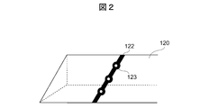
- FIG. 2 is an enlarged view of the vicinity of the side substrate 120 where the ground wiring 122 is formed.
- the ground wiring 122 is provided with a through hole 123 in the middle of the wiring.
- the through hole 123 is provided so as to be connected to a ground layer (corresponding to a ground layer 223 in FIG. 8 described later) formed inside the side substrate 120.
- the ground wiring 122 can supply ground to the ground layer inside the side substrate 120 via the through hole 123.
- through holes similar to the through holes 123 of FIG. 2 are formed, and the ground wiring 132 and the ground wiring 142 are connected to the ground layer via the through holes.
- a main substrate 110 and a printed circuit board (for example, corresponding to the printed circuit board 220 in FIG. 4 and the printed circuit board 230 in FIG. 5) including each of the side substrates 120, 130, and 140 are manufactured.
- the main substrate 110 is a printed circuit board having a multilayer structure in which a ground layer is formed.
- the signal wiring 111 and the ground wiring 112 are formed on the uppermost surface 110A, and the signal wiring 113 and the ground wiring 114 are formed on the lowermost surface 110B.
- the printed circuit board including each of the side substrates 120, 130, and 140 a printed circuit board having a multilayer structure that is sufficiently thinner than the main substrate 110 is used.
- the thickness of the main board 110 is 3 mm
- the thickness of the printed board including each of the side boards 120, 130, and 140 is 0.3 mm or less.
- signal wiring 121, 131, 141 of the corresponding side substrate 120, 130, 140 and ground wiring 122, 132, 142 are formed.
- the printed circuit board 220 including the side board 120 will be described.
- the signal wiring 121 is formed on the signal wiring 111 on the main board 110 and the side board 130 when the side board 120 is bonded to the main board 110 and the side board 130.
- a pattern is formed at a predetermined position to be connected to the signal wiring 131.
- the ground wiring 122 is located at a predetermined position so as to be connected to the ground wiring 112 on the main substrate 110 and the ground wiring 132 on the side substrate 130 when the side substrate 120 is bonded to the main substrate 110 and the side substrate 130.
- a wiring pattern is formed.
- step S101 after forming the signal wiring and the ground wiring on each substrate, a coating process may be performed to protect the signal wiring and the ground wiring by covering them with a solder resist.
- a coating process may be performed to protect the signal wiring and the ground wiring by covering them with a solder resist.
- an appropriate distance between the components is prevented so that a component other than the connection target is soldered and a short circuit does not occur in a soldering process (step S105) described later. Is preferably taken into account.
- step S102 the side substrates 120, 130, and 140 are cut out from the printed circuit board produced in step S101 by cutting each printed circuit board into a predetermined shape.
- step S102 the process of step S102 will be described.
- the side substrate 120 is cut out from a printed circuit board 220 as shown in FIG. 4, for example.
- the printed circuit board 220 is a multilayer printed circuit board manufactured in step S101, and a signal layer 221, a prepreg 222, a ground layer 223, and an insulating layer 224 are formed in this order from the surface side.
- a predetermined signal wiring pattern and a ground wiring pattern are formed on the signal layer 221.
- the cut surface 225 and the cut surface 226 form an angle of 45 degrees with respect to each layer.
- the configuration below the ground layer 223 is not particularly limited, and may be an arbitrary layer configuration.
- the side substrate 120 By cutting such a printed circuit board 220 along the cut surface 225 and the cut surface 226, the side substrate 120 has a triangular shape (inner angles of 45 degrees, 45 degrees, and 90 degrees) when viewed from the side surface. Cut out.
- the cut out portion of the signal layer 221 corresponds to the signal wiring 121 shown in FIG.
- the printed circuit board 220 When the printed circuit board 220 is cut along an oblique cut surface (for example, the cut surface 225), there is a method in which the printed circuit board 220 is tilted and fixed so that the cut surface 225 is in the vertical direction and then cut. Conceivable.
- the printed circuit board including the side substrate 140 manufactured in step S101 is cut along the oblique cut surface to thereby form the side substrate.
- the side substrate 140 can be cut out from the printed circuit board including 140.
- the side board 130 is cut out from a printed board 230 as shown in FIG. 5, for example.
- the printed circuit board 230 is a multilayer printed circuit board manufactured in step S ⁇ b> 101 and has the same layer structure as the printed circuit board 220.
- the cut surface 235 and the cut surface 236 form an angle of 90 degrees with respect to each layer.
- the side substrate 130 is cut into a rectangular shape when viewed from the side surface (the inner angles are all 90 degrees).
- FIG. 6 is a cross-sectional view of the side substrates 120, 130, and 140 and the main substrate 110 before bonding, in which the signal wiring formation portion is taken as a cross section.
- the layer configuration between the ground layer 213 and the ground layer 215 is omitted.
- adhesive resins 252 and 253 having insulating properties are applied to one surface of each of the side substrate 120 and the side substrate 140, and the bonding surfaces are bonded.
- step S104 an insulating adhesive resin 251 is applied to the bonding surface of the main substrate 110, and the assembled substrate composed of the side substrates 120, 130, and 140 bonded in step S103 is bonded to the main substrate 110 (step S104).
- the side substrates 120, 130, and 140 are bonded to the side surfaces of the main substrate 110 by the procedure of step S104.
- FIG. 7 shows a cross section after bonding the substrates shown in FIG.
- the application range of the resins 251 to 253 shown in FIG. 6 is an example.
- the resin 251 to 253 may be applied to the other adhesive surface or may be applied to both adhesive surfaces.
- another insulating adhesive may be used instead of the resins 251 to 253, another insulating adhesive may be used. Step S103 and step S104 may be switched in order.
- the wires for example, the signal wire 111 and the signal wire 121 are not connected to each other, and the wires may be discontinuous between the substrates. .
- soldering is performed on the connection portion of the signal wiring between the substrates (step S105).
- the gaps between the substrates are connected by solder having electrical conductivity, and the signal wiring 111, the signal wiring 121, the signal wiring 131, the signal wiring 141, and the signal wiring 113 become a continuous signal wiring.
- FIG. 8 is a cross-sectional view of the side substrates 120, 130, and 140 and the main substrate 110 before bonding, with the ground wiring forming portion taken as a cross section.
- the side substrates 120 and 140 are bonded to the side substrate 130 shown in FIG. 8 (step S103), and the assembled substrate including the side substrates 120, 130, and 140 is further bonded to the main substrate 110 (step S104). 1 is in the state shown in FIG. Thereafter, soldering is performed in the gaps between the substrates (step S105), whereby the ground wiring 112, the ground wiring 122, the ground wiring 132, the ground wiring 142, and the ground wiring 114 become a continuous ground wiring.
- the through hole for connecting the ground wiring formed in the surface and a ground layer is shown.
- the ground wiring 122 on the surface and the ground layer 223 are connected via a through hole 123.
- the through hole 133 of the side substrate 130 and the through hole 143 of the side substrate 140 shown in FIGS. 8 and 9 are also the same through holes as the through hole 123.
- the main substrate 110 is also grounded. Through holes are provided between the wiring 112 and the ground layer 213 and between the ground wiring 114 and the ground layer 215.
- FIG. 10 is an enlarged perspective view of a bonding portion between the main substrate 110 and the side substrate 120.
- the signal wirings 111 and 121 and the ground wirings 112 and 122 shown in FIG. 10 are coated with a solder resist on the surfaces thereof.
- the end 115 is one end of the signal wiring 111
- the end 116 is one end of the ground wiring 112
- the end 125 is one end of the signal wiring 121
- the end 126 is one end of the ground wiring 122.
- These end portions 115, 116, 125, and 126 are portions that are not covered with a solder resist and have exposed conductive portions (for example, copper).
- both ends of the wiring to be connected are soldered.
- the end 115 and the end 125 are connected by the solder 261
- the end 116 and the end 126 are connected by the solder 262.
- the end portions of the respective wirings are soldered as in FIG. After soldering each end, a coating process with a solder resist may be performed.
- the signal wirings 111, 121, 131,. 141 and 113 and the ground wirings 112, 122, 132, 142, and 114 may be subjected to a coating process with a solder resist.
- the printed wiring board 1 that connects the signal wiring 111 formed on the uppermost surface 110A of the main substrate 110 and the signal wiring 113 formed on the lowermost surface 110B by the signal wirings 121, 131, and 141 by the above manufacturing procedure. Produced. At this time, in the printed wiring board 1, the ground wiring 112 formed on the uppermost surface 110 ⁇ / b> A and the ground wiring 114 formed on the lowermost surface 110 ⁇ / b> B are also continuously connected by the ground wirings 122, 132, and 142.
- Steps S101 to S105 include processes such as formation of wiring and cutting of the printed circuit board. Specific methods for performing these processes include widely used printed circuit boards such as sputtering and resist coating. Therefore, detailed description thereof is omitted. The same applies to a method of manufacturing a printed wiring board according to another embodiment described later.
- the printed wiring board 1 includes a plurality of side boards in which the signal wirings 121, 131, and 141 are provided on the side surfaces of the main board 110 and the surface layers.
- the signal wirings 111 and 113 formed in different wiring layers of the main substrate 110 can be connected to the signals of the side substrates 120, 130, and 140 without providing through holes and vias in the signal wiring portion.
- the wirings 121, 131, and 141 can be connected. As a result, it is possible to realize a signal wiring that connects different wiring layers while preventing deterioration of waveform quality during signal transmission due to impedance mismatching.
- each connecting portion of the main substrate 110 and the side substrate 130 is 90 degrees and the angle of each connecting portion of the side substrate 120 and the side substrate 140 is 45 degrees, Are all 135 degrees as shown in FIG. That is, the bending angles in the series of signal wirings 111, 121, 131, 141, 113 are all 135 degrees.
- the wiring bend angle is 135 degrees or more. Therefore, the signal wiring can be connected between different wiring layers while minimizing the influence on the waveform quality during high-speed signal transmission caused by distortion of the signal wiring.
- the bending angle of the wiring may be less than 135 degrees as long as it is an obtuse angle.
- the printed wiring board 1 is slightly affected by the waveform quality at the time of high-speed signal transmission, but it is possible to perform high-speed transmission with reduced deterioration of the waveform quality. A certain level of waveform quality can be maintained.
- a printed wiring board according to the second embodiment uses a smaller number of side boards than the printed wiring board 1 according to the first embodiment, and is used for different wiring layers of the main board. It is characterized in that the formed signal wiring is connected.
- the printed circuit board 3 includes a main board 310 and two side boards 320 and 330.
- the main board 310 is a printed board having the signal wiring 311 and the ground wiring 312 in the wiring layer on the uppermost surface and the signal wiring 313 and the ground wiring 314 in the wiring layer on the lowermost surface.
- the manufacturing method of the main substrate 310 is the same as that of the main substrate 110 in the first embodiment.
- the side board 320 is a printed board having a signal wiring 321 and a ground wiring 322 on the surface.
- the side substrate 330 is a printed circuit board having signal wirings 331 and ground wirings 332 on the surface. Note that the side substrate 330 illustrated in FIG. 11 has the same shape and size as the side substrate 320.
- the side substrates 320 and 330 are produced by cutting out from the printed circuit board including the side substrates 320 and 330, respectively, similarly to the side substrates 120, 130, and 140 in the first embodiment.
- FIG. 12 shows the printed circuit board 340 before the side substrate 320 is cut out.
- a signal layer 341, a prepreg 342, a ground layer 343, and an insulating layer 344 are formed in this order from the surface side.
- the cut surface 345 makes an angle of 60 degrees with respect to each layer, and the cut surface 346 makes an angle of 30 degrees with each layer.
- the side substrate 320 is cut into a triangular shape (the inner angle is 30 degrees, 60 degrees, and 90 degrees) as viewed from the side surface. Is issued. Further, since the side substrate 330 has the same shape and size as the side substrate 320, the side substrate 330 can be manufactured by performing the same process as cutting the side substrate 320 from the printed board 340.
- the printed circuit board 3 is bonded to the main board 310 and the side boards 320 and 330 by using insulating resins 351 and 352 having insulating properties. It is formed.
- soldering using electrically conductive solder is performed on each connection portion of the signal wirings 311, 313, 321, and 331 on the main substrate 310 and the side substrates 320 and 330.
- the signal wiring 311 is connected to the signal wiring 313 via the signal wiring 321 and the signal wiring 331.
- Such a printed wiring board 3 is formed on different wiring layers of the main board 310 using two side boards 320 and 330 that are fewer than the side boards (side boards 120, 130, and 140) of the printed wiring board 1. Since the signal wiring 311 and the signal wiring 313 can be connected, in addition to the effect of the printed wiring board 1 according to the first embodiment, the design process is simplified, the manufacturing time is shortened, and the manufacturing cost is reduced. You can expect. In particular, when the side substrates 320 and 330 have the same shape and size as shown in FIG. 12, it is only necessary to fabricate one type of side substrate 320, which simplifies the design process and the fabrication time. Can be further expected.
- the bending angle of each connection portion of the signal wirings 311, 321, 331, and 313 in the printed wiring board 3 is 120 degrees and does not satisfy the preferable condition of 135 degrees or more.
- the effect on the waveform quality is small compared to the case where the signal wiring is connected through the through hole.
- the printed wiring board 3 has special effects in terms of design process, production time, and manufacturing cost as described above. Accordingly, when it is desired to connect signal wirings formed in different wiring layers, when emphasizing waveform quality, the printed wiring board 1 according to the first embodiment is selected, and the design process, manufacturing time, and manufacturing cost are selected based on the waveform quality. When importance is attached to the printed wiring board 3, the printed wiring board 3 according to the second embodiment may be selected.
- a printed wiring board according to a third embodiment has signal wiring formed on the main board and signal wiring formed on a small board located on the main board on the surface. The connection is made using a relay board having signal wiring.
- the printed wiring board 4 includes a main board 410, a relay board 420, and a small board 430.
- the main board 410 is a printed board having a signal wiring 411 formed on the surface thereof.
- the small substrate 430 has the same configuration as that of the main substrate 410, and the signal wiring 431 is formed on the surface.
- the relay substrate 420 has the same shape and structure as the side substrate 120 in the first embodiment, and the signal wiring 421 is formed on the surface.
- the main substrate 410 and the small substrate 430 can be manufactured by the same manufacturing method as the main substrate 110 of the printed wiring board 1, and the relay substrate 420 is manufactured by the same manufacturing method as the side substrate 120 of the printed wiring board 1. be able to.
- the relay substrate 420 and the small substrate 430 are bonded to the main substrate 410 using the adhesive resins 441 and 442 having insulating properties so that the positional relationship shown in FIG. 14 is obtained, and the signal wiring 411 at the connection portion of each substrate. , 421, 431 are soldered using solder having electrical conductivity.
- the signal wiring 411 is connected to the signal wiring 431 via the signal wiring 421, and a continuous signal wiring from the signal wiring 411 to the signal wiring 431 is formed.
- the angle formed by the signal wiring 411 and the signal wiring 421 and the angle formed by the signal wiring 421 and the signal wiring 431 are both 135 degrees.
- the signal wiring can be obtained by bonding the relay board 420 on which the signal wiring 421 is formed. Since 421 forms an obtuse angle and is connected to the signal wirings 411 and 431, it is possible to realize a signal wiring that connects different wiring layers while preventing deterioration of waveform quality during signal transmission due to impedance mismatch.
- a printed wiring board according to a fourth embodiment has a groove portion in the signal wiring formation region of the side board for the side board connecting the signal wirings formed in different wiring layers of the main board. And the bent portion of the signal wiring is curved.
- the printed wiring board 5 is formed by bonding a main board 510 and two side boards 520 and 530.
- the main substrate 510 has a signal wiring 511 in the wiring layer on the uppermost surface and a signal wiring 512 in the wiring layer on the lowermost surface.
- the side substrate 520 has a signal wiring 521 on the surface and a ground layer 522 inside.
- the side substrate 530 has a signal wiring 531 on the surface and a ground layer 532 inside.
- the main substrate 510 and the side substrates 520 and 530 can be manufactured by the same manufacturing method as the printed wiring board 1 or the printed wiring board 2 except the formation of a groove and a curved surface described later.
- the side substrates 520 and 530 have groove portions in the regions where the signal wirings 521 and 531 are formed. Further, as shown in FIG. 15, the side substrates 520 and 530 are connected to the connection regions 5A, 5B and 5C. A curved surface portion is formed.
- the curved surface portion can be formed by molding a predetermined position of the surface layer before cutting the side substrate 520, 530 from each printed circuit board including the side substrate 520, 530 in the process of manufacturing the side substrate 520, 530.
- the groove portion can be formed by, for example, melting a part of the surface layer before forming the signal wiring on each printed board including the side substrates 520 and 530.
- each of the connection regions 5A, 5B, and 5C is formed using an electrically conductive solder.
- soldering the connection portion of the signal wiring the printed wiring board 5 on which one continuous signal wiring from the signal wiring 511 to the signal wiring 512 is formed is manufactured.
- the signal wirings 511 and 512 formed in different wiring layers can be connected without using through holes or vias. Therefore, it is possible to realize signal wiring that connects different wiring layers while preventing deterioration in waveform quality during signal transmission due to impedance mismatch of through holes and vias.
- the signal wirings 521 and 531 are formed in the groove portions of the side substrates 520 and 530 in the printed wiring board 5, the signal wirings 521 and 531 are formed at positions lower than the surrounding surface layer. The effect which reduces the danger of the disconnection with respect to 521,531 can be anticipated.
- the signal wirings 521, 531 are formed on the curved surface portions formed in the connection regions 5A, 5B, 5C of the side substrates 520, 530, the signal wirings 511, 521, 531
- the signal wiring can be connected in a curved manner at each connection portion 512.
- the bending angle of the signal wiring becomes larger than that when the linear signal wiring is connected, and an effect of further reducing the influence on the waveform quality due to reflection or the like can be expected.
- the present invention is not limited to this, and, for example, four or more.
- the signal wiring 111 and the signal wiring 113 of the main board 110 may be connected using the side substrate.
- the bending angle at the connecting portion between the signal wirings can be increased by increasing the number of the side boards.
- the effect of further reducing the influence of signal reflection in transmission and maintaining waveform quality can be expected.
- the number of such side boards is not limited to the printed wiring board 1 according to the first embodiment, and the same applies to the printed wiring boards 3 to 5 according to the second to fourth embodiments.
- the present invention is not limited to this.
- one side cut out from a printed board into a predetermined shape is used. It may be constituted by a substrate.
- the signal wiring is formed on the surface of the side board after being cut out from the printed board.
- a side substrate may be used to connect signal wirings formed inside different main substrates.
- the side substrate when the side substrate is bonded to the main substrate, the side substrate may be bonded to a position where the signal wiring of the side substrate is connected to the signal wiring of the main substrate.
- the present invention is not limited thereto, and the signal wiring is not limited thereto. What is necessary is just to be connected in the state in which signal transmission is possible.
- an electrode may be provided at a connection portion of the signal wiring, and each signal wiring may be connected to the electrode.
- the ground wiring may be formed on the main board and connected to the ground wiring of the side board.
- the main substrate 110 on which the signal wiring 111 and the signal wiring 113 are formed has the first signal wiring and the second signal wiring formed on different wiring layers.
- the assembled substrate obtained by bonding the side substrates 120, 130, and 140 in step S103 of FIG. 3 is bonded to the first printed circuit board, and the third signal wiring is formed on the surface. This corresponds to 2 printed circuit boards.
- Each of the side substrates 120, 130, and 140 corresponds to a plurality of third printed circuit boards having signal wirings formed on the surface thereof.
Landscapes
- Engineering & Computer Science (AREA)
- Microelectronics & Electronic Packaging (AREA)
- Production Of Multi-Layered Print Wiring Board (AREA)
Abstract
【課題】 インピーダンス不整合による信号伝送時の波形品質の劣化を防止しながら、異なる配線層間の信号配線を接続する。 【解決手段】 プリント配線基板1は、異なる配線層に第1の信号配線111及び第2の信号配線113が形成された第1のプリント基板110と、第1のプリント基板110に接着され、表面に第3の信号配線121,131,141が形成された第2のプリント基板120,130,140とを備える。プリント配線基板1では、第3の信号配線121,131,141が第1の信号配線111及び第2の信号配線113に鈍角をなして接続されることによって、第1の信号配線111から第2の信号配線113まで連続する信号配線を形成する。
Description
本発明は、プリント配線基板に関し、プリント配線基板に適用して好適なものである。
従来、プリント基板では各層に信号配線が形成されるが、プリント基板の異なる配線層に形成された信号配線を接続する場合には、プリント基板の上下面を貫通するスルーホールを形成し、当該スルーホールを経由して信号配線を接続することが一般的であった。
通常、プリント基板に形成される信号配線は、一定(もしくは所定の上下限範囲内)のインピーダンスに保持される。例えば、信号配線が異なる配線層間で接続される場合でも、プリント基板上の各配線層は、接続元の配線層におけるインピーダンスと接続先の配線層におけるインピーダンスとが一定幅のインピーダンスに収まるように形成される。
しかし、層間の接続部に相当するスルーホール部分では、インピーダンスを配線層部分のインピーダンスと一致させることが難しいことが従来から知られており、スルーホールの接続部分でインピーダンスの不整合が発生しやすい。
同一の信号配線内でインピーダンスの不整合が発生すると、反射によって信号波形が歪められ、波形品質が低下してしまう。特に、高速信号の伝送においてはインピーダンスの不整合による波形品質への影響が大きく、場合によっては信号伝送を困難にする要因となる。従って、高速信号の波形品質を維持するためには、インピーダンスを極力一定にすることが好ましい。
このような問題を解決する方法の一例として、特許文献1には、埋め込みビアを使用して配線層を変更するプリント板の製造方法が記載されている。特許文献1に記載されたプリント基板の製造方法では、スルーホールのように基板の上下面を貫通させずに、長さを必要最小限にしたビアを層間部に埋め込むことによって、インピーダンス不整合の影響を低減することができる。
しかし、特許文献1に記載されたプリント基板の製造方法では、配線の層間部に埋め込みビアを使用することによってスルーホールを使用する場合よりはインピーダンス不整合の影響を低減することができるが、埋め込みビアの長さに応じてインピーダンス不整合が発生し得る。異なる配線層を接続する場合に埋め込みビアの長さをなくすことは不可能であるから、特許文献1に記載されたプリント基板の製造方法では、インピーダンス不整合の影響によって、信号伝送時の波形品質が劣化してしまうという問題がある。
本発明は以上の点を考慮してなされたもので、インピーダンス不整合による信号伝送時の波形品質の劣化を防止しながら、異なる配線層間の信号配線を接続し得るプリント配線基板を提案しようとするものである。
かかる課題を解決するため本発明においては、異なる配線層に第1の信号配線及び第2の信号配線が形成された第1のプリント基板と、前記第1のプリント基板に接着され、表面に第3の信号配線が形成された第2のプリント基板とを備え、前記第3の信号配線が前記第1の信号配線及び前記第2の信号配線に鈍角をなして接続されることによって、前記第1の信号配線から前記第2の信号配線まで連続する信号配線を形成するプリント配線基板が提供される。
本発明によれば、インピーダンス不整合による信号伝送時の波形品質の劣化を防止しながら、異なる配線層間の信号配線を接続することができる。
(1)第1の実施の形態
第1の実施の形態によるプリント配線基板は、表層部に信号配線を設けた複数枚の側基板を主基板の側面部に接着することにより、信号配線部分にスルーホールやビアを設けることなく、主基板の異なる配線層に形成された信号配線を接続することを特徴としている。
第1の実施の形態によるプリント配線基板は、表層部に信号配線を設けた複数枚の側基板を主基板の側面部に接着することにより、信号配線部分にスルーホールやビアを設けることなく、主基板の異なる配線層に形成された信号配線を接続することを特徴としている。
(1-1)本実施の形態によるプリント配線基板の構成
図1において、1は全体として第1の実施の形態によるプリント配線基板を示す。プリント配線基板1は、図1に示すように、プリント基板である主基板110の側面に、別のプリント基板である側基板120、130及び140が接着された構造を有している。
図1において、1は全体として第1の実施の形態によるプリント配線基板を示す。プリント配線基板1は、図1に示すように、プリント基板である主基板110の側面に、別のプリント基板である側基板120、130及び140が接着された構造を有している。
主基板110の最上層表面110Aには信号配線111及びグラウンド配線112が形成され、最下層表面110Bには信号配線113及びグラウンド配線114が形成されている。そして、側基板120の表面には信号配線121及びグラウンド配線122が形成され、側基板130の表面には信号配線131及びグラウンド配線132が形成され、側基板140の表面には信号配線141及びグラウンド配線142が形成されている。
図1に示すように主基板110の側面に側基板120、130及び140が接着された場合に、主基板110と側基板120との間では、信号配線111と信号配線121とが鈍角をなして接続し、連続した信号配線となり、グラウンド配線112とグラウンド配線122とが鈍角をなして接続し、連続したグラウンド配線となる。同様に、側基板120と側基板130、側基板130と側基板140、及び、側基板140と主基板110との間において、信号配線及びグラウンド配線は、隣り合う基板上の信号配線又はグラウンド配線同士で鈍角をなして接続し、連続した配線を形成する。この結果、プリント配線基板1においては、信号配線111、信号配線121、信号配線131、信号配線141、そして信号配線113の順に連続した1本の信号配線が形成され、グラウンド配線112、グラウンド配線122、グラウンド配線132、グラウンド配線142、そしてグラウンド配線114の順に連続した1本のグラウンド用の配線が形成される。
本実施の形態の場合は、隣接する基板間の角度が135度となるように主基板110に側基板120、130及び140を接着することによって、連続した信号配線における信号配線111,121,131,141,113による各接続部分(曲げ部分)の角度を全て135度とし、高速信号の伝送時に信号配線の曲げ部分で信号反射が発生することを防止している。
図2は、側基板120のグラウンド配線122が形成された付近を拡大した図である。図2に示すように、グラウンド配線122には、配線の途中にスルーホール123が設けられている。スルーホール123は、側基板120の内部に形成されるグラウンド層(後述する図8のグラウンド層223に相当)に接続するように設けられる。スルーホール123を設けることによって、グラウンド配線122は、スルーホール123を経由して側基板120の内部のグラウンド層にグラウンド供給をすることができる。なお、側基板130及び140においても、図2のスルーホール123と同様のスルーホールがそれぞれ形成され、グラウンド配線132及グラウンド配線142が、スルーホールを経由してグラウンド層に接続される。
(1-2)作製方法
次に、図3を参照して、図1に示したプリント配線基板1の作成手順について説明する。まず、主基板110と、側基板120,130,140のそれぞれを含むプリント基板(例えば、図4のプリント基板220や図5のプリント基板230に相当)とを作製する。主基板110には、内部にグラウンド層が形成された多層構造のプリント基板を用い、最上層表面110Aに信号配線111及びグラウンド配線112を形成し、最下層表面110Bに信号配線113及びグラウンド配線114を形成する。
次に、図3を参照して、図1に示したプリント配線基板1の作成手順について説明する。まず、主基板110と、側基板120,130,140のそれぞれを含むプリント基板(例えば、図4のプリント基板220や図5のプリント基板230に相当)とを作製する。主基板110には、内部にグラウンド層が形成された多層構造のプリント基板を用い、最上層表面110Aに信号配線111及びグラウンド配線112を形成し、最下層表面110Bに信号配線113及びグラウンド配線114を形成する。
また、側基板120,130,140のそれぞれを含むプリント基板には、主基板110よりも十分な薄さを有する多層構造のプリント基板を用いる。一例として、主基板110の厚さを3mmとすれば、側基板120,130,140のそれぞれを含むプリント基板の厚さは0.3mm以下にする。そして、各プリント基板には、対応する側基板120,130,140の信号配線121,131,141、及びグラウンド配線122,132,142を形成する。例えば、側基板120を含むプリント基板220について説明すると、信号配線121は、側基板120が主基板110及び側基板130に接着された場合に主基板110上の信号配線111及び側基板130上の信号配線131に接続するような所定の位置にパターン形成される。また、グラウンド配線122は、側基板120が主基板110及び側基板130に接着された場合に主基板110上のグラウンド配線112及び側基板130上のグラウンド配線132に接続するような所定の位置に配線パターンが形成される。
なお、ステップS101では、各基板上に信号配線及びグラウンド配線を形成した後に、当該信号配線及びグラウンド配線の表面をソルダレジストで覆って保護する被覆処理を行ってもよい。また、プリント基板に信号配線及びグラウンド配線を形成する位置については、後述するはんだ付け工程(ステップS105)で、接続対象以外の部品がはんだ付けされてショートが発生しないように、適度な部品間距離を考慮することが好ましい。
次に、ステップS101で作製したプリント基板について、それぞれのプリント基板を所定の形状に切断することにより、側基板120,130,140をそれぞれ切出す(ステップS102)。以下に、ステップS102の処理について説明する。
側基板120は、例えば図4に示すようなプリント基板220から切出される。プリント基板220は、ステップS101で作製された多層構造のプリント基板であって、表面側から順に、信号層221、プリプレグ222、グラウンド層223、及び絶縁層224が形成されている。信号層221には、所定の信号配線パターンやグラウンド配線パターンが形成されている。図4では、切断面225及び切断面226は、各層に対して45度の角度をなす。また、グラウンド層223より下部は、特にその構成を限定されず、任意の層構成であってよい。このようなプリント基板220を切断面225及び切断面226に沿って切断することにより、側基板120は、側面から見た形が三角形(内角の大きさが45度,45度,90度)に切出される。なお、プリント基板220のうち、信号層221の切り出された部分が、図1に示す信号配線121に相当する。
なお、プリント基板220を斜めの切断面(例えば切断面225)に沿って切断する場合には、切断面225が垂直方向になるようにプリント基板220を傾けて固定してから切断するといった方法が考えられる。
そして、プリント基板220から側基板120を切出すのと同様に、ステップS101で作製した、側基板140を含むプリント基板について、当該プリント基板を斜めの切断面に沿って切断することにより、側基板140を含むプリント基板から側基板140を切出すことができる。
また、側基板130は、例えば図5に示すようなプリント基板230から切出される。プリント基板230は、ステップS101で作製された多層構造のプリント基板であって、プリント基板220と同様の層構造を有する。図5では、切断面235及び切断面236は、各層に対して90度の角度をなす。プリント基板230を切断面235及び切断面236に沿って切断することにより、側基板130は、側面から見た形が長方形(内角の大きさが全て90度)に切出される。
次に、ステップS102で切出した側基板130に、同じくステップS102で切出した側基板120及び側基板140を接着する(ステップS103)。図6は、接着前の側基板120,130,140と主基板110について、信号配線の形成部分を断面とする断面図である。図6に示す主基板110では、グラウンド層213とグラウンド層215との間の層構成が省略されている。ステップS103では、例えば図6に示すように、側基板120及び側基板140のそれぞれ1つの面に絶縁性を有する接着用の樹脂252,253を塗布し、接着面を接着する。
次いで、主基板110の接着面に絶縁性を有する接着用の樹脂251を塗布し、ステップS103で接着した側基板120,130,140からなる組基板を主基板110に接着する(ステップS104)。ステップS104の手順によって、主基板110の側面部に側基板120,130,140が接着される。図7は、図6に示す各基板を接着した後の断面を示している。
なお、図6に示した樹脂251~253の塗布範囲は一例であり、例えば、他方の接着面に塗布したり、両方の接着面に塗布したりしてもよい。また、樹脂251~253の代わりに、絶縁性を有する他の接着剤を用いてもよい。また、ステップS103とステップS104とは、順序を入れ替えても構わない。
ここで、接着後の各基板間に隙間が存在する場合には、配線同士(例えば信号配線111と信号配線121)が接続されず、基板間で配線が不連続となってしまう可能性がある。このような配線の不連続を防ぐために、各基板間における信号配線の接続部分にはんだ付けを行う(ステップS105)。その結果、各基板間の隙間が電気伝導性を有するはんだによって接続されて、信号配線111、信号配線121、信号配線131、信号配線141、及び信号配線113が連続した信号配線となる。
上記のステップS103~S105では、信号配線の形成部分を断面とする図6及び図7を参照し、主基板110及び側基板120,130,140について接着やはんだ付けを行うことにより連続した信号配線が形成されることを示したが、同時に、連続したグラウンド配線も形成される。図8は、接着前の側基板120,130,140と主基板110について、グラウンド配線の形成部分を断面とする断面図である。図8に示す側基板130に側基板120,140を接着し(ステップS103)、さらに側基板120,130,140からなる組基板を主基板110に接着する(ステップS104)ことによって、プリント配線基板1は、図9に示す状態となる。その後、各基板間の隙間にはんだ付けを行う(ステップS105)ことによって、グラウンド配線112、グラウンド配線122、グラウンド配線132、グラウンド配線142、及びグラウンド配線114が連続したグラウンド配線となる。
なお、図8及び図9では、表面に形成されたグラウンド配線とグラウンド層とを接続するためのスルーホールが示されている。例えば基板120について、表面のグラウンド配線122とグラウンド層223とは、スルーホール123を介して接続されている。図8及び図9に示す側基板130のスルーホール133及び側基板140のスルーホール143も、スルーホール123と同様のスルーホールであり、また、図示していないが、主基板110においても、グラウンド配線112とグラウンド層213との間や、グラウンド配線114とグラウンド層215との間にスルーホールが設けられる。表面にグラウンド配線を形成した場合にスルーホールでグラウンド層に接続して接地をとることは一般的な技術であるので、作製方法については説明を省略する。
図10は、主基板110と側基板120との接着部分を拡大した斜視図である。図10に示す信号配線111,121及びグラウンド配線112,122は、その表面にソルダレジストによる被覆処理が行われているとする。端部115は信号配線111の一端であり、端部116はグラウンド配線112の一端であり、端部125は信号配線121の一端であり、端部126はグラウンド配線122の一端である。これらの端部115,116,125,126は、それぞれソルダレジストによる被覆がなく、導電部(例えば、銅)が露出している部分とする。図3のステップS105では、接続する配線の両端部をはんだ付けする。具体的には、端部115と端部125とをはんだ261によって接続し、端部116と端部126とをはんだ262によって接続する。他の基板間の隙間に対するはんだ付けにおいても、図10と同様に、各配線の端部同士をはんだ付けする。各端部をはんだ付けした後は、ソルダレジストによる被覆処理を行ってもよい。
なお、ステップS101の手順の際に各配線にソルダレジストによる被覆処理を行うのではなく、例えば、図3に示す全ての手順が完了した後に、プリント配線基板1の信号配線111,121,131,141,113及びグラウンド配線112,122,132,142,114に対してソルダレジストによる被覆処理を行うとしてもよい。
上記の作製手順によって、主基板110の最上層表面110Aに形成された信号配線111と最下層表面110Bに形成された信号配線113とを信号配線121,131,141によって接続するプリント配線基板1が作製される。またこのとき、プリント配線基板1では、最上層表面110Aに形成されたグラウンド配線112と最下層表面110Bに形成されたグラウンド配線114とについても、グラウンド配線122,132,142によって連続して接続される。
なお、ステップS101~S105では配線の形成やプリント基板の切断といった工程を含むが、これらの工程を行うための具体的な方法は、スパッタリングやレジスト塗布等、広く一般的に行われているプリント基板の作製方法を利用することができるので、その詳細な説明を省略する。これは、後述する他の実施の形態によるプリント配線基板の作製方法についても同様である。
(1-3)第1の実施の形態の効果
上述したように、プリント配線基板1は、主基板110の側面部に、表層部に信号配線121,131,141を設けた複数枚の側基板120,130,140を接着することにより、信号配線部分にスルーホールやビアを設けることなく、主基板110の異なる配線層に形成された信号配線111,113を側基板120,130,140の信号配線121,131,141を介して接続することができる。その結果、インピーダンス不整合による信号伝送時の波形品質の劣化を防止しながら、異なる配線層間を接続する信号配線を実現することができる。
上述したように、プリント配線基板1は、主基板110の側面部に、表層部に信号配線121,131,141を設けた複数枚の側基板120,130,140を接着することにより、信号配線部分にスルーホールやビアを設けることなく、主基板110の異なる配線層に形成された信号配線111,113を側基板120,130,140の信号配線121,131,141を介して接続することができる。その結果、インピーダンス不整合による信号伝送時の波形品質の劣化を防止しながら、異なる配線層間を接続する信号配線を実現することができる。
また、主基板110及び側基板130のそれぞれの接続部分の角度が90度で、側基板120及び側基板140のそれぞれの接続部分の角度が45度であることから、プリント配線基板1において基板同士がなす角度は、図7に示すように全て135度となる。すなわち、一連の信号配線111,121,131,141,113における曲げ角度は全て135度となる。一般に、高速信号の伝送時に波形品質に対する信号反射等の影響を抑えるためには、配線の曲げ角度を135度以上にすることが望ましいとされているが、プリント配線基板1は、この135度以上という曲げ角度の条件を満たすことから、信号配線の歪曲を原因とする高速信号伝送時の波形品質に対する影響を最小限に抑えつつ、異なる配線層間で信号配線を接続することができる。
なお、プリント配線基板1においては、配線の曲げ角度は、鈍角であれば135度未満であってもよい。配線の曲げ角度が135度未満の鈍角である場合には、プリント配線基板1は、高速信号の伝送時の波形品質に対する影響を若干受けるが、波形品質の劣化を低減させて高速伝送が可能な程度の波形品質を維持できる。
(2)第2の実施の形態
第2の実施の形態によるプリント配線基板は、第1の実施の形態によるプリント配線基板1よりも少ない個数の側基板を用いて、主基板の異なる配線層に形成された信号配線を接続することを特徴としている。
第2の実施の形態によるプリント配線基板は、第1の実施の形態によるプリント配線基板1よりも少ない個数の側基板を用いて、主基板の異なる配線層に形成された信号配線を接続することを特徴としている。
図11に示すように、第2の実施の形態によるプリント基板3は、主基板310と2つの側基板320,330とを備える。主基板310は、最上層表面の配線層に信号配線311及びグラウンド配線312を有し、最下層表面の配線層に信号配線313及びグラウンド配線314を有するプリント基板である。主基板310の作製方法は、第1の実施の形態における主基板110と同様である。
側基板320は、表面に信号配線321及びグラウンド配線322を有するプリント基板である。また、側基板330は、表面に信号配線331及びグラウンド配線332を有するプリント基板である。なお、図11に示す側基板330は、側基板320と同じ形状及び大きさを有する。
側基板320,330は、第1の実施の形態における側基板120,130,140と同様に、それぞれ側基板320,330を含むプリント基板から切出されて作製される。図12は、側基板320が切出される前のプリント基板340を示している。プリント基板340には、表面側から順に、信号層341、プリプレグ342、グラウンド層343、及び絶縁層344が形成されている。図12では、切断面345は各層に対して60度の角度をなし、切断面346は各層に対して30度の角度をなす。そして、プリント基板340を切断面345及び切断面346に沿って切断することにより、側基板320は、側面から見た形が三角形(内角の大きさが30度,60度,90度)に切出される。また、側基板330について、側基板330は側基板320と同じ形状及び大きさを有するので、プリント基板340から側基板320を切出すのと同じ工程を行うことによって側基板330を作製できる。
第2の実施の形態では、図13に示すように、主基板310及び側基板320,330を、絶縁性を有する接着用の樹脂351,352を用いて接着することによって、プリント配線基板3が形成される。また、主基板310及び側基板320,330における信号配線311,313,321,331の各接続部分には、電気伝導性を有するはんだを用いたはんだ付けが行われる。その結果、プリント配線基板3では、信号配線311が、信号配線321及び信号配線331を介して信号配線313に接続される。
このようなプリント配線基板3は、プリント配線基板1の側基板(側基板120,130,140)よりも少ない2つの側基板320,330を用いて、主基板310の異なる配線層に形成された信号配線311と信号配線313とを接続することができるので、第1の実施の形態によるプリント配線基板1の効果に加えて、設計工程の簡易化、作製時間の短縮、及び製造コストの低減を期待することができる。また特に、図12に示したように側基板320,330を同じ形状及び大きさとする場合には、1種類の側基板320を2枚作製すればよいことから、設計工程の簡易化及び作製時間の短縮を更に期待することができる。
なお、プリント配線基板3における信号配線311,321,331,313の各接続部分の曲げ角度は120度となり、135度以上という好適な条件を満たさないことから、ある程度波形品質への影響は免れないが、スルーホールによって信号配線を接続した場合に比べると波形品質への影響は小さい。また、プリント配線基板3は、上述したように設計工程、作製時間、及び製造コストの面で特別な効果を有する。従って、異なる配線層に形成された信号配線を接続したい場合に、波形品質を重視するときには第1の実施の形態によるプリント配線基板1を選択し、波形品質より設計工程、作製時間、及び製造コストを重視するときには第2の実施の形態によるプリント配線基板3を選択すればよい。
(3)第3の実施の形態
第3の実施の形態によるプリント配線基板は、主基板に形成された信号配線と、主基板上に位置する小基板に形成された信号配線とを、表面に信号配線を有する中継基板を用いて接続することを特徴としている。
第3の実施の形態によるプリント配線基板は、主基板に形成された信号配線と、主基板上に位置する小基板に形成された信号配線とを、表面に信号配線を有する中継基板を用いて接続することを特徴としている。
図14に示すように、プリント配線基板4は、主基板410、中継基板420、及び小基板430を備える。主基板410は、表面に信号配線411が形成されたプリント基板である。小基板430も主基板410と同様の構成を有し、表面に信号配線431が形成されている。また、中継基板420は、第1の実施の形態における側基板120と同じ形状及び構造を有し、表面に信号配線421が形成されている。
主基板410及び小基板430は、プリント配線基板1の主基板110と同様の作製方法によって作製することができ、中継基板420は、プリント配線基板1の側基板120と同様の作製方法によって作製することができる。
そして、図14に示す位置関係になるよう、絶縁性を有する接着性の樹脂441,442を用いて主基板410に中継基板420及び小基板430を接着し、各基板の接続部分の信号配線411,421,431に、電気伝導性を有するはんだを用いたはんだ付けを行う。その結果、プリント配線基板4では、信号配線411が信号配線421を介して信号配線431に接続され、信号配線411から信号配線431まで連続する信号配線が形成される。なお、図14では、信号配線411と信号配線421とがなす角度、及び、信号配線421と信号配線431とがなす角度は、ともに135度である。
このようなプリント配線基板4では、異なるプリント基板上に形成された信号配線411と信号配線431との間であっても、信号配線421が形成された中継基板420を接着することによって、信号配線421が鈍角をなして信号配線411,431に接続するので、インピーダンス不整合による信号伝送時の波形品質の劣化を防止しながら、異なる配線層間を接続する信号配線を実現することができる。
(4)第4の実施の形態
第4の実施の形態によるプリント配線基板は、主基板の異なる配線層に形成された信号配線を接続する側基板について、側基板の信号配線の形成領域に溝部を設け、更に、信号配線の曲げ部分を曲線とすることを特徴としている。
第4の実施の形態によるプリント配線基板は、主基板の異なる配線層に形成された信号配線を接続する側基板について、側基板の信号配線の形成領域に溝部を設け、更に、信号配線の曲げ部分を曲線とすることを特徴としている。
図15に示すように、第4の実施の形態によるプリント配線基板5は、主基板510と2つの側基板520,530とが接着されて形成される。主基板510は、最上層表面の配線層に信号配線511を有し、最下層表面の配線層に信号配線512を有する。側基板520は、表面に信号配線521を有し、内部にグラウンド層522を有する。側基板530は、表面に信号配線531を有し、内部にグラウンド層532を有する。主基板510及び側基板520,530は、後述する溝部と曲面部の形成以外は、プリント配線基板1又はプリント配線基板2と同様の作製方法で作製することができる。
ここで側基板520,530は、図16に示すように、信号配線521,531が形成される領域に溝部を有し、更に図15に示すように、接続領域5A,5B,5Cの部分で曲面部が形成されている。曲面部は、側基板520,530の作製過程で、側基板520,530を含むそれぞれのプリント基板から側基板520,530を切出す前に、表面層の所定の位置を成形することによって形成できる。また、溝部は、側基板520,530を含むそれぞれのプリント基板に信号配線を形成する前に、例えば表面層の一部を溶かすことにより形成できる。
そして、プリント基板から切出された側基板520,530を、絶縁性を有する接着用樹脂によって主基板510に接着した後に、電気伝導性を有するはんだを用いて接続領域5A,5B,5Cの各信号配線の接続部分をはんだ付けすることにより、信号配線511から信号配線512まで連続した1本の信号配線が形成されたプリント配線基板5が作製される。
このようなプリント配線基板5では、第1の実施の形態によるプリント配線基板1と同様に、スルーホールやビアを用いることなく異なる配線層に形成された信号配線511,512を接続することができるので、スルーホールやビアのインピーダンス不整合による信号伝送時の波形品質の劣化を防止しながら、異なる配線層間を接続する信号配線を実現することができる。
さらに、プリント配線基板5は、側基板520,530の溝部に信号配線521,531が形成されることにより、周囲の表面層よりも低い位置に信号配線521,531が形成されるので、信号配線521,531に対する断線の危険性を低減する効果が期待できる。
またさらに、プリント配線基板5では、信号配線521,531が側基板520,530の接続領域5A,5B,5Cに形成された曲面部の上に形成されるので、信号配線511,521,531,512の各接続部分において、曲線的に信号配線を接続することができる。その結果、信号配線の曲げ角度は直線状の信号配線を接続した場合よりも大きくなり、反射等による波形品質への影響を更に低減する効果が期待できる。
(5)他の実施の形態
なお、上述の第1の実施の形態においては、3つの側基板120,130,140を用いる場合について述べたが、本発明はこれに限らず、例えば4つ以上の側基板を用いて主基板110の信号配線111と信号配線113とを接続するように構成されてもよい。このような場合に、水平積層型のプリント基板から切出した側基板を用いる場合に、側基板の枚数を増やすことによって、信号配線同士の接続部分における曲げ角度をより大きくすることができるので、高速伝送における信号反射等の影響をさらに低減して波形品質を維持する効果が期待できる。また、このような側基板の個数は、第1の実施の形態によるプリント配線基板1に限定されず、第2~第4の実施の形態によるプリント配線基板3~5についても同様である。
なお、上述の第1の実施の形態においては、3つの側基板120,130,140を用いる場合について述べたが、本発明はこれに限らず、例えば4つ以上の側基板を用いて主基板110の信号配線111と信号配線113とを接続するように構成されてもよい。このような場合に、水平積層型のプリント基板から切出した側基板を用いる場合に、側基板の枚数を増やすことによって、信号配線同士の接続部分における曲げ角度をより大きくすることができるので、高速伝送における信号反射等の影響をさらに低減して波形品質を維持する効果が期待できる。また、このような側基板の個数は、第1の実施の形態によるプリント配線基板1に限定されず、第2~第4の実施の形態によるプリント配線基板3~5についても同様である。
また、上述の第1~第3の実施の形態においては、複数の側基板を用いる場合について述べたが、本発明はこれに限らず、例えば、プリント基板から所定の形状に切出した1つの側基板によって構成されてもよい。ただし、このような場合には、プリント基板から切出した後の側基板の表面に信号配線が形成されるように留意する必要がある。
また、上述の第1、第2及び第4の実施の形態においては、主基板又は小基板の表面に形成された信号配線を接続するために側基板を用いる場合について述べたが、本発明はこれに限らず、例えば、主基板の異なる内部に形成される信号配線を接続するために側基板を用いるように構成されてもよい。このような場合には、側基板を主基板に接着するときに、側基板の信号配線が主基板の信号配線に接続されるような位置に側基板を接着すればよく、その結果、表面に限らず、異なる配線層に形成された信号配線を接続可能なプリント配線基板を実現することができる。
また、上述の第1~第4の実施の形態においては、各信号配線の接続部分に電気伝導性を有するはんだによるはんだ付けを行う場合について述べたが、本発明はこれに限らず、信号配線間で信号伝送が可能な状態に接続されればよい。例えば、信号配線の接続部分に電極を設け、それぞれの信号配線を電極に接続する等してもよい。
また、上述の第1の実施の形態においては、信号配線111と信号配線113とを接続するだけでなく、グラウンド配線112とグラウンド配線114とを接続する場合についても述べたが、本発明はこれに限らず、例えば、第2~第4の実施の形態によるプリント配線基板3~5においても同様に、主基板にグラウンド配線を形成し、側基板のグラウンド配線と接続するようにしてもよい。
また、上述の第1の実施の形態において、信号配線111及び信号配線113が形成された主基板110は、異なる配線層に第1の信号配線と第2の信号配線とが形成された第1のプリント基板に相当し、図3のステップS103で側基板120,130,140が接着されてなる組基板は、第1のプリント基板に接着され、表面に第3の信号配線が形成された第2のプリント基板に相当する。そして、それぞれの側基板120,130,140は、表面に信号配線が形成された複数の第3のプリント基板に相当する。
1,3,4,5 プリント配線基板
110,310,410,510 主基板
120,130,140,320,330,520,530 側基板
420 中継基板
430 小基板
111,113,121,131,141,311,313,321,331,411,421,431,511,512,521,531 信号配線
112,114,122,132,142 グラウンド配線
123,133,143 スルーホール
220,230,340 プリント基板
251,252,253,351,352,441,442 樹脂
261,262 はんだ
110,310,410,510 主基板
120,130,140,320,330,520,530 側基板
420 中継基板
430 小基板
111,113,121,131,141,311,313,321,331,411,421,431,511,512,521,531 信号配線
112,114,122,132,142 グラウンド配線
123,133,143 スルーホール
220,230,340 プリント基板
251,252,253,351,352,441,442 樹脂
261,262 はんだ
Claims (8)
- 異なる配線層に第1の信号配線及び第2の信号配線が形成された第1のプリント基板と、
前記第1のプリント基板に接着され、表面に第3の信号配線が形成された第2のプリント基板と
を備え、
前記第3の信号配線が前記第1の信号配線及び前記第2の信号配線に鈍角をなして接続されることによって、前記第1の信号配線から前記第2の信号配線まで連続する信号配線を形成する
ことを特徴とするプリント配線基板。 - 前記第2のプリント基板は、表面に信号配線が形成された複数の第3のプリント基板からなり、
前記複数の第3のプリント基板は、隣接する第3のプリント基板間で前記信号配線が鈍角をなして連続して接続するように互いが接着される
ことを特徴とする請求項1に記載のプリント配線基板。 - 前記第2のプリント基板は溝部を有し、前記第3の信号配線は前記溝部に形成される
ことを特徴とする請求項1に記載のプリント配線基板。 - 前記第2のプリント基板は前記第1のプリント基板との接続部分に曲面部を有し、前記第3の信号配線の端部は前記曲面部に形成される
ことを特徴とする請求項1に記載のプリント配線基板。 - 前記第1から第3の信号配線による各接続部分が、電気伝導性を有するはんだによってはんだ付けされる
ことを特徴とする請求項1に記載のプリント配線基板。 - 前記第1のプリント基板と前記第2のプリント基板とが、絶縁性を有する樹脂によって接着される
ことを特徴とする請求項1に記載のプリント配線基板。 - 前記第2のプリント基板は、表面に形成されたグラウンド配線と、内部に形成されたグラウンド層と、前記グラウンド配線と前記グラウンド層とを接続するスルーホールとを更に有する
ことを特徴とする請求項1に記載のプリント配線基板。 - 前記第1のプリント基板は、前記第1の信号配線が形成された第4のプリント基板と前記第2の信号配線が形成された第5のプリント基板とからなる
ことを特徴とする請求項1に記載のプリント配線基板。
Priority Applications (1)
| Application Number | Priority Date | Filing Date | Title |
|---|---|---|---|
| PCT/JP2012/066616 WO2014002238A1 (ja) | 2012-06-28 | 2012-06-28 | プリント配線基板 |
Applications Claiming Priority (1)
| Application Number | Priority Date | Filing Date | Title |
|---|---|---|---|
| PCT/JP2012/066616 WO2014002238A1 (ja) | 2012-06-28 | 2012-06-28 | プリント配線基板 |
Publications (1)
| Publication Number | Publication Date |
|---|---|
| WO2014002238A1 true WO2014002238A1 (ja) | 2014-01-03 |
Family
ID=49782467
Family Applications (1)
| Application Number | Title | Priority Date | Filing Date |
|---|---|---|---|
| PCT/JP2012/066616 WO2014002238A1 (ja) | 2012-06-28 | 2012-06-28 | プリント配線基板 |
Country Status (1)
| Country | Link |
|---|---|
| WO (1) | WO2014002238A1 (ja) |
Citations (7)
| Publication number | Priority date | Publication date | Assignee | Title |
|---|---|---|---|---|
| JPS57190672U (ja) * | 1981-05-28 | 1982-12-03 | ||
| JP2001326441A (ja) * | 2000-05-17 | 2001-11-22 | Sony Corp | 複合配線板及びその製造方法 |
| JP2003158353A (ja) * | 2001-11-26 | 2003-05-30 | Ngk Spark Plug Co Ltd | 配線基板 |
| JP2004342890A (ja) * | 2003-05-16 | 2004-12-02 | Alps Electric Co Ltd | 電子回路ユニット |
| JP2006040870A (ja) * | 2004-02-20 | 2006-02-09 | Matsushita Electric Ind Co Ltd | 接続部材および実装体、ならびにその製造方法 |
| JP2006147901A (ja) * | 2004-11-22 | 2006-06-08 | Murata Mfg Co Ltd | 積層電子部品、その製造方法およびその特性測定方法 |
| JP2012119446A (ja) * | 2010-11-30 | 2012-06-21 | Yamaichi Electronics Co Ltd | フレキシブル配線板 |
-
2012
- 2012-06-28 WO PCT/JP2012/066616 patent/WO2014002238A1/ja active Application Filing
Patent Citations (7)
| Publication number | Priority date | Publication date | Assignee | Title |
|---|---|---|---|---|
| JPS57190672U (ja) * | 1981-05-28 | 1982-12-03 | ||
| JP2001326441A (ja) * | 2000-05-17 | 2001-11-22 | Sony Corp | 複合配線板及びその製造方法 |
| JP2003158353A (ja) * | 2001-11-26 | 2003-05-30 | Ngk Spark Plug Co Ltd | 配線基板 |
| JP2004342890A (ja) * | 2003-05-16 | 2004-12-02 | Alps Electric Co Ltd | 電子回路ユニット |
| JP2006040870A (ja) * | 2004-02-20 | 2006-02-09 | Matsushita Electric Ind Co Ltd | 接続部材および実装体、ならびにその製造方法 |
| JP2006147901A (ja) * | 2004-11-22 | 2006-06-08 | Murata Mfg Co Ltd | 積層電子部品、その製造方法およびその特性測定方法 |
| JP2012119446A (ja) * | 2010-11-30 | 2012-06-21 | Yamaichi Electronics Co Ltd | フレキシブル配線板 |
Similar Documents
| Publication | Publication Date | Title |
|---|---|---|
| US9042114B2 (en) | Electronic component | |
| KR102023338B1 (ko) | 프린트 배선판 | |
| JP4987764B2 (ja) | 方向性結合器 | |
| US8091218B2 (en) | Method of manufacturing a rigid printed wiring board | |
| US8624130B2 (en) | Circuit board having grown metal layer in a flexible zone | |
| JP4414365B2 (ja) | 高速伝送用基板 | |
| US9445493B2 (en) | Signal line and manufacturing method therefor | |
| US10219367B2 (en) | Multilayer resin substrate, and method of manufacturing multilayer resin substrate | |
| WO2015087893A1 (ja) | 信号伝送部品および電子機器 | |
| JP2012182437A (ja) | 配線基板及びその製造方法 | |
| US9788437B2 (en) | Method for manufacturing printed circuit board with etching process to partially remove conductive layer | |
| WO2013099286A1 (ja) | 多層配線基板 | |
| US8071885B2 (en) | Printed circuit board | |
| JP4683381B2 (ja) | 回路基板 | |
| US10091879B2 (en) | Conductor connecting structure and mounting board | |
| KR100762395B1 (ko) | 고주파 임피던스 매칭이 가능한 인쇄회로기판 및 그 제조방법 | |
| CN103338590A (zh) | 软性电路板及其制造方法 | |
| JP6344476B2 (ja) | 多層回路基板 | |
| WO2014002238A1 (ja) | プリント配線基板 | |
| US20110247871A1 (en) | Multi-layer printed circuit board comprising film and method for fabricating the same | |
| JP4340700B2 (ja) | 電線複合プリント配線基板、電線複合プリント配線基板製造方法、電線部品、電線部品製造方法、および電子機器 | |
| JP7071244B2 (ja) | 多層印刷配線板 | |
| JP6063785B2 (ja) | 回路基板、回路基板の製造方法 | |
| KR102088323B1 (ko) | 인쇄회로기판의 결합구조 | |
| JP6996948B2 (ja) | 高周波伝送線路 |
Legal Events
| Date | Code | Title | Description |
|---|---|---|---|
| 121 | Ep: the epo has been informed by wipo that ep was designated in this application |
Ref document number: 12879783 Country of ref document: EP Kind code of ref document: A1 |
|
| NENP | Non-entry into the national phase |
Ref country code: DE |
|
| 122 | Ep: pct application non-entry in european phase |
Ref document number: 12879783 Country of ref document: EP Kind code of ref document: A1 |
|
| NENP | Non-entry into the national phase |
Ref country code: JP |