WO2013175742A1 - Imaging device - Google Patents
Imaging device Download PDFInfo
- Publication number
- WO2013175742A1 WO2013175742A1 PCT/JP2013/003135 JP2013003135W WO2013175742A1 WO 2013175742 A1 WO2013175742 A1 WO 2013175742A1 JP 2013003135 W JP2013003135 W JP 2013003135W WO 2013175742 A1 WO2013175742 A1 WO 2013175742A1
- Authority
- WO
- WIPO (PCT)
- Prior art keywords
- pixels
- trenches
- substrate
- shielding material
- light shielding
- Prior art date
Links
- 238000003384 imaging method Methods 0.000 title claims description 4
- 239000000758 substrate Substances 0.000 claims abstract description 92
- 239000000463 material Substances 0.000 claims description 78
- 239000011810 insulating material Substances 0.000 claims description 9
- RYGMFSIKBFXOCR-UHFFFAOYSA-N Copper Chemical compound [Cu] RYGMFSIKBFXOCR-UHFFFAOYSA-N 0.000 claims description 7
- 229910052581 Si3N4 Inorganic materials 0.000 claims description 7
- VYPSYNLAJGMNEJ-UHFFFAOYSA-N Silicium dioxide Chemical compound O=[Si]=O VYPSYNLAJGMNEJ-UHFFFAOYSA-N 0.000 claims description 7
- GWEVSGVZZGPLCZ-UHFFFAOYSA-N Titan oxide Chemical compound O=[Ti]=O GWEVSGVZZGPLCZ-UHFFFAOYSA-N 0.000 claims description 7
- RTAQQCXQSZGOHL-UHFFFAOYSA-N Titanium Chemical compound [Ti] RTAQQCXQSZGOHL-UHFFFAOYSA-N 0.000 claims description 7
- NRTOMJZYCJJWKI-UHFFFAOYSA-N Titanium nitride Chemical compound [Ti]#N NRTOMJZYCJJWKI-UHFFFAOYSA-N 0.000 claims description 7
- 229910052782 aluminium Inorganic materials 0.000 claims description 7
- XAGFODPZIPBFFR-UHFFFAOYSA-N aluminium Chemical compound [Al] XAGFODPZIPBFFR-UHFFFAOYSA-N 0.000 claims description 7
- 229910052802 copper Inorganic materials 0.000 claims description 7
- 239000010949 copper Substances 0.000 claims description 7
- 229910000449 hafnium oxide Inorganic materials 0.000 claims description 7
- WIHZLLGSGQNAGK-UHFFFAOYSA-N hafnium(4+);oxygen(2-) Chemical compound [O-2].[O-2].[Hf+4] WIHZLLGSGQNAGK-UHFFFAOYSA-N 0.000 claims description 7
- 239000007769 metal material Substances 0.000 claims description 7
- TWNQGVIAIRXVLR-UHFFFAOYSA-N oxo(oxoalumanyloxy)alumane Chemical compound O=[Al]O[Al]=O TWNQGVIAIRXVLR-UHFFFAOYSA-N 0.000 claims description 7
- BPUBBGLMJRNUCC-UHFFFAOYSA-N oxygen(2-);tantalum(5+) Chemical compound [O-2].[O-2].[O-2].[O-2].[O-2].[Ta+5].[Ta+5] BPUBBGLMJRNUCC-UHFFFAOYSA-N 0.000 claims description 7
- HQVNEWCFYHHQES-UHFFFAOYSA-N silicon nitride Chemical compound N12[Si]34N5[Si]62N3[Si]51N64 HQVNEWCFYHHQES-UHFFFAOYSA-N 0.000 claims description 7
- 229910052814 silicon oxide Inorganic materials 0.000 claims description 7
- 229910001936 tantalum oxide Inorganic materials 0.000 claims description 7
- 239000010936 titanium Substances 0.000 claims description 7
- 229910052719 titanium Inorganic materials 0.000 claims description 7
- OGIDPMRJRNCKJF-UHFFFAOYSA-N titanium oxide Inorganic materials [Ti]=O OGIDPMRJRNCKJF-UHFFFAOYSA-N 0.000 claims description 7
- WFKWXMTUELFFGS-UHFFFAOYSA-N tungsten Chemical compound [W] WFKWXMTUELFFGS-UHFFFAOYSA-N 0.000 claims description 7
- 229910052721 tungsten Inorganic materials 0.000 claims description 7
- 239000010937 tungsten Substances 0.000 claims description 7
- 238000000034 method Methods 0.000 abstract description 5
- 230000000903 blocking effect Effects 0.000 abstract 2
- 239000007787 solid Substances 0.000 abstract 1
- 230000004048 modification Effects 0.000 description 33
- 238000012986 modification Methods 0.000 description 33
- 238000000926 separation method Methods 0.000 description 11
- 230000009467 reduction Effects 0.000 description 9
- IOCYQQQCJYMWDT-UHFFFAOYSA-N (3-ethyl-2-methoxyquinolin-6-yl)-(4-methoxycyclohexyl)methanone Chemical compound C=1C=C2N=C(OC)C(CC)=CC2=CC=1C(=O)C1CCC(OC)CC1 IOCYQQQCJYMWDT-UHFFFAOYSA-N 0.000 description 4
- 238000009792 diffusion process Methods 0.000 description 4
- 230000008569 process Effects 0.000 description 4
- 239000003086 colorant Substances 0.000 description 3
- 230000035945 sensitivity Effects 0.000 description 3
- XUIMIQQOPSSXEZ-UHFFFAOYSA-N Silicon Chemical compound [Si] XUIMIQQOPSSXEZ-UHFFFAOYSA-N 0.000 description 2
- 238000006243 chemical reaction Methods 0.000 description 2
- 238000004519 manufacturing process Methods 0.000 description 2
- 238000005498 polishing Methods 0.000 description 2
- 229910052710 silicon Inorganic materials 0.000 description 2
- 239000010703 silicon Substances 0.000 description 2
- 239000000126 substance Substances 0.000 description 2
- 230000004075 alteration Effects 0.000 description 1
- 230000015556 catabolic process Effects 0.000 description 1
- 230000000295 complement effect Effects 0.000 description 1
- 230000007547 defect Effects 0.000 description 1
- 238000006731 degradation reaction Methods 0.000 description 1
- 229910003460 diamond Inorganic materials 0.000 description 1
- 239000010432 diamond Substances 0.000 description 1
- 230000000694 effects Effects 0.000 description 1
- 230000006872 improvement Effects 0.000 description 1
- 229910044991 metal oxide Inorganic materials 0.000 description 1
- 150000004706 metal oxides Chemical class 0.000 description 1
- 230000003287 optical effect Effects 0.000 description 1
- 239000004065 semiconductor Substances 0.000 description 1
Images


Classifications
-
- H—ELECTRICITY
- H01—ELECTRIC ELEMENTS
- H01L—SEMICONDUCTOR DEVICES NOT COVERED BY CLASS H10
- H01L27/00—Devices consisting of a plurality of semiconductor or other solid-state components formed in or on a common substrate
- H01L27/14—Devices consisting of a plurality of semiconductor or other solid-state components formed in or on a common substrate including semiconductor components sensitive to infrared radiation, light, electromagnetic radiation of shorter wavelength or corpuscular radiation and specially adapted either for the conversion of the energy of such radiation into electrical energy or for the control of electrical energy by such radiation
- H01L27/144—Devices controlled by radiation
- H01L27/146—Imager structures
- H01L27/14601—Structural or functional details thereof
- H01L27/14603—Special geometry or disposition of pixel-elements, address-lines or gate-electrodes
- H01L27/14605—Structural or functional details relating to the position of the pixel elements, e.g. smaller pixel elements in the center of the imager compared to pixel elements at the periphery
-
- H—ELECTRICITY
- H01—ELECTRIC ELEMENTS
- H01L—SEMICONDUCTOR DEVICES NOT COVERED BY CLASS H10
- H01L27/00—Devices consisting of a plurality of semiconductor or other solid-state components formed in or on a common substrate
- H01L27/14—Devices consisting of a plurality of semiconductor or other solid-state components formed in or on a common substrate including semiconductor components sensitive to infrared radiation, light, electromagnetic radiation of shorter wavelength or corpuscular radiation and specially adapted either for the conversion of the energy of such radiation into electrical energy or for the control of electrical energy by such radiation
- H01L27/144—Devices controlled by radiation
- H01L27/146—Imager structures
- H01L27/14601—Structural or functional details thereof
- H01L27/1463—Pixel isolation structures
Definitions
- the present disclosure relates to image pickup elements and image pickup devices, and more particularly, to an image pickup element and an image pickup device with which color mixing of an image signal obtained by the image pickup element is suppressed and the S/N ratio of the image signal is increased.
- CMOS image sensors (hereinafter referred to as CIS) are used as image pickup elements in, for example, digital still cameras and digital video cameras.
- CIS Complementary metal oxide semiconductor
- a back-illuminated CIS in which a grid-shaped light-shielding material is arranged so as to extend between the adjacent pixels has been proposed.
- this back-illuminated CIS light is incident on a back surface at the side opposite to a front surface on which a wiring layer is formed, and the incident light reaches a photodiode (PD) region of a silicon (Si) substrate without being blocked by the wiring layer. Therefore, the reduction in sensitivity per unit pixel can be suppressed.
- PD photodiode
- obliquely incident light is reflected by the grid-shaped light-shielding material arranged so as to extend between the adjacent pixels, and is suppressed from being incident on pixels other than the pixels on which the light is expected to be incident.
- color mixing can be reduced and reduction in color reproducibility can be suppressed.
- the present disclosure provides an image pickup element in which color mixing of an image signal can be suppressed, the S/N ratio of the image signal can be increased, and reduction in pixel size and increase in pixel density can be achieved at a practically applicable level.
- an image pickup device including a substrate, a plurality of pixels formed in the substrate, and a plurality of trenches formed in the substrate and extending at least partially between pairs of pixels included in the plurality of pixels.
- at least two trenches in the plurality of trenches are formed along at least a first line that extends between a plurality of pixels. In accordance with still other embodiments, no two trenches cross one another.
- the device can additionally include a substrate light shielding material that fills the plurality of trenches.
- a substrate light shielding material that fills the plurality of trenches.
- at least one pixel in the plurality of pixels is not completely surrounded by the substrate light shielding material.
- the substrate light shielding material can further define a perimeter that substantially surrounds each pixel in the plurality of pixels, and with respect to each pixel in the plurality of pixels there is at least one gap in the perimeter formed by the substrate light shielding material.
- the image pickup device can further include an upper layer light shielding material.
- the upper layer light shielding material and the substrate light shielding material can be made from an insulating material, including but not limited to silicon oxide, titanium oxide, silicon nitride, aluminum oxide, tantalum oxide, or hafnium oxide, or a metal material including but not limited to tungsten, aluminum, titanium nitride, titanium, or copper.
- At least two trenches are formed along at least a second line that extends between a plurality of pixels.
- the first line can be one of parallel to and perpendicular to the second line.
- the plurality of pixels are arranged in rows and columns, wherein the first line extends between one of two adjacent rows of pixels and two adjacent columns of pixels.
- each pixel can be associated with at least four trenches.
- an image pickup device includes a substrate, a plurality of pixels, and a plurality of trenches.
- the plurality of trenches are formed in the substrate, wherein at least some of the trenches are between adjacent pairs of pixels, and wherein no one trench extends across any other trench.
- At least some of the trenches included in the plurality of trenches can be formed along a first plurality of parallel lines, wherein more than one trench included in the plurality of trenches is formed along each line in the first plurality of lines. In accordance with still other embodiments, at least some of the trenches are formed along a second plurality of parallel lines, wherein only trench is formed along each line in the second plurality of lines.
- the plurality of pixels can be arranged in rows and columns, wherein the first plurality of parallel lines extend between one of adjacent rows of pixels and adjacent columns of pixels.
- the image pickup device can additionally include a substrate light shielding material, wherein the trenches in the plurality of trenches are filled with the substrate light shielding material.
- the image pickup device can also include an upper layer light shielding material, wherein the upper layer light shielding material extends between the pixels.
- the substrate light shielding material and the upper layer light shielding material can be made of an insulating material including at least one of silicon oxide, titanium oxide, silicon nitride, aluminum oxide, tantalum oxide, or hafnium oxide, or a metal material such as tungsten, aluminum, titanium nitride, titanium, or copper.
- an imaging device including a substrate, a plurality of pixels, a plurality of trenches, and a substrate light shielding material.
- the plurality of pixels are formed in the substrate.
- the plurality of trenches are formed in the substrate, and at least some of the trenches extend between pairs of the pixels.
- the substrate light shielding material fills the trenches included in the plurality of trenches, wherein with respect to each pixel in the plurality of pixels there exists at least one gap in the substrate light shielding material.
- the plurality of pixels can be arranged in rows in columns with respect to a light incident side of the substrate. Moreover, each trench in the plurality of trenches does not intersect any other trench.
- color mixing between the pixels can be suppressed, the S/N ratio can be increased, and a reduction in pixel size and an increase in pixel density can be achieved at a practically applicable level.
- an image can be captured such that color mixing between the pixels is suppressed, the S/N ratio is increased, and a reduction in pixel size and an increase in pixel density are achieved at a practically applicable level.
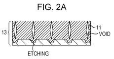
- Fig. 1 illustrates a conventional back-illuminated CIS viewed from a light incident side.
- Fig. 2A is a sectional view of the conventional back-illuminated CIS illustrated in Fig. 1 taken along line IIA-IIA.
- Fig. 2B is a sectional view of the conventional back-illuminated CIS illustrated in Fig. 1 taken along line IIB-IIB.
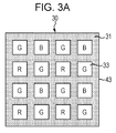
- Fig. 3A illustrates an upper Si layer of a back-illuminated CIS in accordance with embodiments of the present disclosure, viewed from a light incident side;
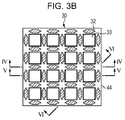
- Fig. 3B illustrates a Si substrate of the back-illuminated CIS in accordance with embodiments of the present disclosure, viewed from a light incident side;
- Fig. 3A illustrates an upper Si layer of a back-illuminated CIS in accordance with embodiments of the present disclosure, viewed from a light incident side;
- Fig. 3B illustrates a Si substrate of the back-illuminated CIS in
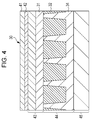
- Fig. 4 is a sectional view of the back-illuminated CIS illustrated in Figs. 3A and 3B taken along line IV-IV;
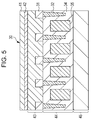
- Fig. 5 is a sectional view of the back-illuminated CIS illustrated in Figs. 3A and 3B taken along line V-V;
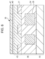
- Fig. 6 is a sectional view of the back-illuminated CIS illustrated in Figs. 3A and 3B taken along line VI-VI;
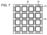
- Fig. 7 illustrates a first modification including a modified trench shape in accordance with embodiments of the present disclosure;
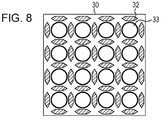
- Fig. 8 illustrates a second modification including a modified pixel shape in accordance with embodiments of the present disclosure;
- FIG. 9 illustrates a third modification including a modified Si upper layer in accordance with embodiments of the present disclosure
- Fig. 10 illustrates a fourth modification with a charge-fixed film in accordance with embodiments of the present disclosure
- Fig. 11 is a graph showing the color mixing characteristics with respect to the incident angle
- Fig. 12A illustrates an example of a fifth modification with modified trenches in accordance with other embodiments of the present disclosure
- Fig. 12B illustrates another example of the fifth modification with modified trenches in accordance with other embodiments of the present disclosure
- Fig. 13 is a graph showing the color mixing characteristics with respect to the incident angle
- Fig. 14A illustrates an example of a sixth modification with modified trenches in accordance with embodiments of the present disclosure
- Fig. 14A illustrates an example of a sixth modification with modified trenches in accordance with embodiments of the present disclosure
- Fig. 14A illustrates an example of a sixth modification with modified trenches in accordance with embodiments of the present disclosure
- FIG. 14B illustrates another example of the sixth modification with modified trenches in accordance with embodiments of the present disclosure
- Fig. 15 illustrates a seventh modification with modified trenches in accordance with embodiments of the present disclosure
- Fig. 16A illustrates an example of an eighth modification with modified trenches in accordance with embodiments of the present disclosure
- Fig. 16B illustrates another example of the eighth modification with modified trenches in accordance with embodiments of the present disclosure
- Fig. 17 illustrates an example of a ninth modification with modified trenches in accordance with embodiments of the present disclosure
- Fig. 18A illustrates another example of a tenth modification with modified trenches in accordance with embodiments of the present disclosure
- Fig. 18A illustrates another example of a tenth modification with modified trenches in accordance with embodiments of the present disclosure
- FIG. 18B illustrates another example of the tenth modification with modified trenches in accordance with embodiments of the present disclosure
- Fig. 18C illustrates another example of the tenth modification with modified trenches in accordance with embodiments of the present disclosure
- Fig. 18D illustrates another example of the tenth modification with modified trenches in accordance with embodiments of the present disclosure
- Fig. 18E illustrates another example of the tenth modification with modified trenches in accordance with embodiments of the present disclosure
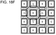
- Fig. 18F illustrates another example of the tenth modification with modified trenches in accordance with embodiments of the present disclosure.
- Fig. 1 illustrates a conventional back-illuminated CIS viewed from a light incident side, the back-illuminated CIS including a grid-shaped light-shielding material arranged so as to extend between the adjacent pixels.
- Figs. 2A and 2B are sectional views of the back-illuminated CIS 10 illustrated in Fig. 1 taken along lines IIA-IIA and IIB-IIB, respectively.
- the conventional back-illuminated CIS 10 includes a grid-shaped trench (groove) formed so as to extend between pixels 12 on a silicon (Si) substrate 13 having a photodiode (PD) region in which photoelectric conversion is performed.
- the trench is filled with a light-shielding material 11.
- the grid-shaped trench includes vertical and horizontal trenches that intersect at crossing portions (hereinafter referred to as trench crossing portions), and various problems occur at the trench crossing portions.
- stress concentration may occur in the Si substrate 13 in regions surrounding the trench crossing portions and serve as a source of noise in the image signal.
- the Si substrate 13 tends to be relatively deeply etched at the trench crossing portions. Accordingly, defects may occur in the trench crossing portions and serve as a source of noise in the image signal.
- insulating film 15 is formed on the Si substrate 13 when the grid-shaped trench is filled with the light-shielding material 11.
- the insulating film 15 degrades the color mixing characteristics when light is obliquely incident thereon.
- the thickness of the insulating film 15 on the Si substrate 13 can be reduced by a chemical mechanical polishing (CMP) process.
- CMP chemical mechanical polishing
- the CMP process is not suitable for mass production since the number of steps and cost will be increased.
- the above-described problems can be solved without performing the CMP process in the production of the back-illuminated CIS.
- Figs. 3A and 3B illustrate a back-illuminated CIS 30 according to an embodiment of the present disclosure viewed from a light incident side.
- Fig. 3A illustrates an upper Si layer 43
- Fig. 3B illustrates a Si substrate 44.
- the back-illuminated CIS 30 has a six-layer structure including an on-chip lens 41, a color filter 42, the Si upper layer 43, the Si substrate 44, and a wiring layer 45 (see Fig. 4) in that order from the light incident side.
- the pixels 33 of the back-illuminated CIS 30 can be arranged in rows and columns so as to form a lattice-type array.
- White squares in Figs. 3A and 3B show the positions of pixels 33, and 'R', 'G', and 'B' written in the white squares in Fig. 3A represent the wavelength ranges of light received by the pixels 33.
- R, G, and B are arranged in a Bayer pattern. However, the arrangement of R, G, and B is not limited to this pattern.
- three primary colors are not limited to R, G, and B, and another color, such as white (W), may be additionally used. This also applies to other embodiments of the present disclosure, including but not limited to those in the following drawings.
- the Si upper layer 43 (layer on the Si substrate 44) includes a grid-shaped Si-upper-layer light-shielding material 31 formed so as to extend between the pixels 33.
- trenches are formed in the Si substrate 44 so as to extend between the adjacent pixels 33 and so that no trench crossing portions are formed.
- the trenches are filled with a Si-substrate light-shielding material 32, which is made of a light-shielding material.
- the Si-upper-layer light-shielding material 31 and the Si-substrate light-shielding material 32 may be made of, for example, an insulating material such as silicon oxide, titanium oxide, silicon nitride, aluminum oxide, tantalum oxide, or hafnium oxide, or a metal material such as tungsten, aluminum, titanium nitride, titanium, or copper.
- an insulating material such as silicon oxide, titanium oxide, silicon nitride, aluminum oxide, tantalum oxide, or hafnium oxide
- a metal material such as tungsten, aluminum, titanium nitride, titanium, or copper.
- Figs. 4, 5, and 6 are sectional views of the back-illuminated CIS 30 illustrated in Figs. 3A and 3B taken along lines IV-IV, V-V, and VI-VI, respectively.
- the back-illuminated CIS 30 has a six-layer structure including the on-chip lens 41, the color filter 42, the Si upper layer 43, the Si substrate 44, and the wiring layer 45 in that order from the light incident side.
- the on-chip lens 41 collects light incident thereon and directs the incident light to photoelectric converters included in the Si substrate 44.
- the color filter 42 transmits only light in specific wavelength ranges.
- the Si upper layer 43 includes the Si-upper-layer light-shielding material 31.
- the Si substrate 44 has a photodiode (PD) region in which a P-type diffusion layer 34 and an N-type diffusion layer 35 are arranged.
- the wiring layer 45 outputs electric charges generated in the PD region to a subsequent stage as an electrical signal.
- the trenches are formed in the Si substrate 44 so that no trench crossing portions are formed, and are filed with the Si-substrate light-shielding material 32. Therefore, the problems due to the trench crossing portions in the back-illuminated CIS 10 according to the related art do not occur.
- edges in the Si substrate 44 may be formed so as to extend through the Si substrate 44 in a partial or entire area of the Si substrate 44.
- Fig. 7 illustrates an embodiment of the present disclosure with a modification to the shape of the ends of the trenches formed in the Si substrate 44.
- the trenches shown in Fig. 3B have pointed ends, the trenches may instead have flat ends as illustrated in Fig. 7.
- the trenches may instead have arc-shaped or concave ends.
- Fig. 8 illustrates an embodiment of the present disclosure with a modification to the shape of the pixels (Si substrate openings).
- the pixels (Si substrate openings) 33 are square-shaped in Figs. 3A and 3B, the pixels (Si substrate openings) 33 may instead be circular shaped, as illustrated in Fig. 8.
- the pixels (Si substrate openings) 33 may instead be diamond or polygonal shaped.
- the light shielding performance of oblique portions may be increased by forming the pixels (Si substrate openings) 33 in a circular or polygonal shape.
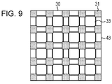
- Fig. 9 illustrates an embodiment of the present disclosure with a modification to the shape of the Si-upper-layer light-shielding material 31 included in the Si upper layer 43.
- the Si-upper-layer light-shielding material 31 is grid-shaped in Fig. 3A, the Si-upper-layer light-shielding material 31 may instead be provided only at locations where the Si-substrate light-shielding material 32 is not provided (that is, locations corresponding to trench crossing portions), as illustrated in Fig. 9.
- the area of the Si substrate openings 33 is increased, so that the sensitivity of the PD region may be increased.
- the width of the Si-upper-layer light-shielding material 31 may be smaller than or equal to the width of the Si-substrate light-shielding material 32. The width may also be partially changed.
- Fig. 10 illustrates an embodiment of the present disclosure with a modification in which a charge-fixed film 51 is additionally provided.
- the charge-fixed film 51 which has a negative fixed charge, may be provided around the Si-substrate light-shielding material 32 and on the back surface (upper surface in Fig. 10) of the Si substrate 44.
- an inversion layer is formed on a Si boundary surface that is in contact with the charge-fixed film 51. Holes in the inversion layer recombine with electrons in a dark current that may be generated along the boundary surface, so that the influence of the dark current may be suppressed.
- the back-illuminated CIS 30 illustrated in Figs. 3A and 3B includes no trench crossing portions, which serve as a noise source (source of white spot or dark current).
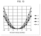
- Fig. 11 is a graph showing the color mixing characteristics with respect to the incident angle of light.
- the horizontal axis represents the incident angle of light.
- the vertical axis represents the result of subtraction of the ratio of an output from a red (R) pixel to an output from a green (G) pixel when green (G) light is incident at 0 degrees from the ratio of an output from the red (R) pixel to an output from the green (G) pixel when green (G) light is incident at various incident angles.
- the curve L1 in the graph shows the color mixing characteristics of a back-illuminated CIS in which a grid-shaped trench is formed so as to extend between pixels.
- the curve L2 in the graph shows the color mixing characteristics of a back-illuminated CIS in which a grid-shaped trench is formed so as to extend between pixels and the thickness of an insulating film (film of light-shielding material) formed on a Si substrate and made of a light-shielding material with which the trench is filled is reduced by a chemical mechanical polishing (CMP) process.
- CMP chemical mechanical polishing
- the curve L3 in the graph shows the color mixing characteristics of the back-illuminated CIS 30 illustrated in Figs. 3A and 3B.
- the higher the values along the vertical axis the greater the degradation of the color mixing characteristics.
- the color mixing characteristics are improved as the upward opening of the U-shaped curves L1 to L3 is increased.
- the color mixing characteristics of the back-illuminated CIS 30 illustrated in Figs. 3A and 3B are worse than those of the back-illuminated CIS in which the grid-shaped trench is formed so as to extend between the pixels. Modifications in which the color mixing characteristics are improved without forming the trench crossing portions will now be described.
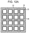
- Figs. 12A and 12B illustrate examples of a modification in which trenches extending in vertical and horizontal directions are alternately arranged in a grid-shaped region that extends between the pixels.
- Fig. 12A shows the case in which the trenches have pointed ends.
- Fig. 12B shows the case in which the trenches have flat ends.
- Fig. 13 is a graph in which a curve L4 showing the color mixing characteristics according to the fifth modification is added to the graph shown in Fig. 11. As is clear from Fig. 13, according to the fifth modification, the color mixing characteristics are improved compared to those of the back-illuminated CIS 30 illustrated in Fig. 3.
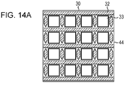
- Figs. 14A and 14B illustrate examples of embodiments of the present disclosure with modifications in which trenches that continuously extend in one of horizontal and vertical directions and trenches that intermittently extend in the other one of the horizontal and vertical directions are formed in a grid-shaped region that extends between the pixels.
- Fig. 14A shows the case in which trenches that continuously extend in the horizontal direction are formed.
- Fig. 14B shows the case in which trenches that continuously extend in the vertical direction are formed.
- the trenches may have different depths. In such a case, the trenches extending in the horizontal and vertical directions may be formed so as to have the same depth by adjusting the widths of the trenches.
- Fig. 15 illustrates an embodiment of the present disclosure with a modification in which the trenches are formed so as to include portions having different widths so that the volume thereof does not increase at diagonal ends of each pixel.
- Figs. 16A and 16B illustrate examples of embodiments of the present disclosure with modifications in which the trenches that cross each other are connected to each other at an angle less than or equal to a crossing angle (90 degrees) at diagonal ends of each pixel.
- Fig. 17 illustrates embodiments of the present disclosure with modifications in which separation locations at which the trenches are separated into segments are changed in accordance with the view angle direction so that the trenches are not separated into segments at many locations with respect to a direction in which light is inclined.
- Figs. 18A to 18F show examples of embodiments of the present disclosure with modifications in which symmetry of the separation locations of the trenches is not set for each pixel and particular pixels (B pixels that receive light with the longest wavelength or R pixels that receive light with the shortest wavelength) are surrounded by the trenches.
- the back-illuminated CIS 30 includes the color filter 42 in which the three primary colors are arranged in a Bayer pattern to output a color image signal.
- the three primary colors may instead be arranged in any pattern, including but not limited to a stripe pattern.
- the color filter 42 may incorporate white filter elements.
- the color filter 42 may be omitted when a monochrome image signal is to be output.
- the trenches formed in the Si substrate 44 are filled with the light-shielding material.
- the trenches may have a hollow structure instead of being filled with the light-shielding material.
- the back-illuminated CIS 30 according to the present embodiment may be installed not only in cameras, such as digital still cameras and digital video cameras, but also in smart phones, mobile phones, various personal computers, etc., having a function of capturing still and moving images.
- An image pickup device comprising: a substrate; a plurality of pixels formed in the substrate; and a plurality of trenches formed in the substrate and extending at least partially between pairs of pixels included in the plurality of pixels, and wherein at least two trenches in the plurality of trenches are formed along at least a first line that extends between a plurality of pixels.
- the device of (1) wherein no two trenches cross one another.
- the device of (1) further comprising: a substrate light shielding material, wherein the substrate light shielding material fills the plurality of trenches.
- the insulating material including at least one of silicon oxide, titanium oxide, silicon nitride, aluminum oxide, tantalum oxide, or hafnium oxide, or a metal material such a tungsten, aluminum, titanium nitride, titanium, or copper.
- the first line is one of parallel to and perpendicular to the second line.
- the device of (1) wherein the plurality of pixels are arranged in rows and columns, and wherein the first line extends between one of two adjacent rows of pixels and two adjacent columns of pixels.
- each pixel is associated with at least four trenches, and wherein between diagonally opposed pairs of pixels no trench intersects any other trench.
- An image pickup device comprising: a substrate; a plurality of pixels; and a plurality of trenches formed in the substrate, wherein at least some of the trenches are between adjacent pairs of pixels, and wherein no one trench extends across any other trench.
- a substrate light shielding material wherein the trenches in the plurality of trenches are filled with the substrate light shielding material.
- an upper layer light shielding material wherein the upper layer light shielding material extends between the pixels.
- the substrate light shielding material and the upper layer light shielding material are made of an insulating material including at least one of silicon oxide, titanium oxide, silicon nitride, aluminum oxide, tantalum oxide, or hafnium oxide, or a metal material such a tungsten, aluminum, titanium nitride, titanium, or copper.
- a back-illuminated image pickup element comprising: a trench provided between adjacent pixels to block obliquely incident light, the trench having a separation location at which the trench is separated into segments.
- the separation location is provided in a crossing region in which a region that vertically extends between horizontally adjacent pixels and a region that horizontally extends between vertically adjacent pixels cross each other.
- the trench includes a horizontal trench and a vertical trench, and a plurality of the separation locations are symmetrically arranged such that the separation locations are provided at every other pixel in each of the horizontal and vertical trenches.
- the trench includes a horizontal trench and a vertical trench, and a plurality of the separation locations are symmetrically arranged such that the separation locations are provided at every pixel in one of the horizontal and vertical trenches and no separation locations are provided in the other of the horizontal and vertical trenches.
- a plurality of the separation locations are not symmetrically arranged, and wherein the pixels include a pixel that receives light with a longest or shortest wavelength among wavelengths of light receivable by the image pickup element and that is located so as to be surrounded by the trench.
- the trench is filled with a light-shielding material.
- An image pickup device comprising: an image pickup unit including a back-illuminated image pickup element including a trench provided between adjacent pixels to block obliquely incident light, the trench having a separation location at which the trench is separated into segments.
Landscapes
- Physics & Mathematics (AREA)
- Engineering & Computer Science (AREA)
- Power Engineering (AREA)
- Electromagnetism (AREA)
- Condensed Matter Physics & Semiconductors (AREA)
- General Physics & Mathematics (AREA)
- Computer Hardware Design (AREA)
- Microelectronics & Electronic Packaging (AREA)
- Solid State Image Pick-Up Elements (AREA)
- Transforming Light Signals Into Electric Signals (AREA)
Priority Applications (3)
| Application Number | Priority Date | Filing Date | Title |
|---|---|---|---|
| US14/401,396 US10074684B2 (en) | 2012-05-23 | 2013-05-16 | Image pickup device with pixels having non-intersecting substrate trenches therebetween |
| KR1020147030033A KR102115046B1 (ko) | 2012-05-23 | 2013-05-16 | 촬상 장치 |
| CN201380025543.2A CN104303305B (zh) | 2012-05-23 | 2013-05-16 | 成像装置 |
Applications Claiming Priority (2)
| Application Number | Priority Date | Filing Date | Title |
|---|---|---|---|
| JP2012117194A JP6168331B2 (ja) | 2012-05-23 | 2012-05-23 | 撮像素子、および撮像装置 |
| JP2012-117194 | 2012-05-23 |
Publications (1)
| Publication Number | Publication Date |
|---|---|
| WO2013175742A1 true WO2013175742A1 (en) | 2013-11-28 |
Family
ID=48626543
Family Applications (1)
| Application Number | Title | Priority Date | Filing Date |
|---|---|---|---|
| PCT/JP2013/003135 WO2013175742A1 (en) | 2012-05-23 | 2013-05-16 | Imaging device |
Country Status (5)
| Country | Link |
|---|---|
| US (1) | US10074684B2 (ko) |
| JP (1) | JP6168331B2 (ko) |
| KR (1) | KR102115046B1 (ko) |
| CN (1) | CN104303305B (ko) |
| WO (1) | WO2013175742A1 (ko) |
Cited By (2)
| Publication number | Priority date | Publication date | Assignee | Title |
|---|---|---|---|---|
| US10692910B2 (en) | 2016-03-15 | 2020-06-23 | Sony Corporation | Solid-state imaging element and electronic device |
| WO2021039455A1 (en) * | 2019-08-27 | 2021-03-04 | Sony Semiconductor Solutions Corporation | Imaging device, production method, and electronic apparatus |
Families Citing this family (19)
| Publication number | Priority date | Publication date | Assignee | Title |
|---|---|---|---|---|
| JP6303803B2 (ja) | 2013-07-03 | 2018-04-04 | ソニー株式会社 | 固体撮像装置およびその製造方法 |
| TWI660490B (zh) * | 2014-03-13 | 2019-05-21 | 日商半導體能源研究所股份有限公司 | 攝像裝置 |
| FR3030884B1 (fr) * | 2014-12-19 | 2016-12-30 | Stmicroelectronics (Grenoble 2) Sas | Structure de pixel a multiples photosites |
| JP6570844B2 (ja) * | 2015-02-26 | 2019-09-04 | 株式会社東芝 | 光検出器、その製造方法、放射線検出器、および放射線検出装置 |
| US9653511B2 (en) | 2015-08-11 | 2017-05-16 | Omnivision Technologies, Inc. | CMOS image sensor with peninsular ground contracts and method of manufacturing the same |
| CN108231809A (zh) * | 2017-12-12 | 2018-06-29 | 上海集成电路研发中心有限公司 | 一种背照式图像传感器及其制备方法 |
| JP2019145544A (ja) * | 2018-02-16 | 2019-08-29 | ソニーセミコンダクタソリューションズ株式会社 | 撮像素子 |
| JP2020031136A (ja) | 2018-08-22 | 2020-02-27 | キヤノン株式会社 | 撮像装置およびカメラ |
| US11121160B2 (en) | 2018-10-17 | 2021-09-14 | Canon Kabushiki Kaisha | Photoelectric conversion apparatus and equipment comprising a light shielding part in a light receiving region and a light shielding film in a light shielded region |
| US11244978B2 (en) | 2018-10-17 | 2022-02-08 | Canon Kabushiki Kaisha | Photoelectric conversion apparatus and equipment including the same |
| KR20210027780A (ko) * | 2019-09-03 | 2021-03-11 | 에스케이하이닉스 주식회사 | 이미지 센서 |
| TW202137528A (zh) * | 2019-11-13 | 2021-10-01 | 日商索尼半導體解決方案公司 | 固體攝像裝置及其製造方法 |
| JP2021086881A (ja) * | 2019-11-26 | 2021-06-03 | キヤノン株式会社 | 光電変換装置、光電変換装置の製造方法、および機器 |
| US11469264B2 (en) * | 2020-01-30 | 2022-10-11 | Omnivision Technologies, Inc. | Flare-blocking image sensor |
| US11393861B2 (en) * | 2020-01-30 | 2022-07-19 | Omnivision Technologies, Inc. | Flare-suppressing image sensor |
| WO2021215303A1 (ja) * | 2020-04-20 | 2021-10-28 | ソニーセミコンダクタソリューションズ株式会社 | 固体撮像素子および電子機器 |
| CN116897433A (zh) * | 2021-04-15 | 2023-10-17 | 索尼半导体解决方案公司 | 成像装置 |
| JP2022185900A (ja) * | 2021-06-03 | 2022-12-15 | ソニーセミコンダクタソリューションズ株式会社 | 光検出装置及び電子機器 |
| JP2023069162A (ja) * | 2021-11-05 | 2023-05-18 | ソニーセミコンダクタソリューションズ株式会社 | 撮像素子、電子機器 |
Citations (4)
| Publication number | Priority date | Publication date | Assignee | Title |
|---|---|---|---|---|
| US6177293B1 (en) * | 1999-05-20 | 2001-01-23 | Tower Semiconductor Ltd. | Method and structure for minimizing white spots in CMOS image sensors |
| US20090266973A1 (en) * | 2008-04-24 | 2009-10-29 | Stmicroelectronics Crolles 2 Sas | Very small image sensor |
| EP2216818A2 (en) * | 2009-02-10 | 2010-08-11 | Sony Corporation | Solid-state imaging device, method of manufacturing the same, and electronic apparatus |
| EP2320463A1 (fr) * | 2009-11-10 | 2011-05-11 | STmicroelectronics SA | Procédé de formation d'un capteur d'images éclairé par la face arrière |
Family Cites Families (15)
| Publication number | Priority date | Publication date | Assignee | Title |
|---|---|---|---|---|
| JP2004104203A (ja) * | 2002-09-05 | 2004-04-02 | Toshiba Corp | 固体撮像装置 |
| CN1661806A (zh) * | 2004-02-24 | 2005-08-31 | 三洋电机株式会社 | 固体摄像元件和固体摄像元件的制造方法 |
| JP4525144B2 (ja) * | 2004-04-02 | 2010-08-18 | ソニー株式会社 | 固体撮像素子及びその製造方法 |
| JP4505488B2 (ja) * | 2007-09-05 | 2010-07-21 | シャープ株式会社 | 固体撮像素子および電子情報機器 |
| JP4751865B2 (ja) * | 2007-09-10 | 2011-08-17 | 富士フイルム株式会社 | 裏面照射型固体撮像素子及びその製造方法 |
| JP4621719B2 (ja) * | 2007-09-27 | 2011-01-26 | 富士フイルム株式会社 | 裏面照射型撮像素子 |
| JP2009206356A (ja) * | 2008-02-28 | 2009-09-10 | Toshiba Corp | 固体撮像装置およびその製造方法 |
| US20100144084A1 (en) * | 2008-12-05 | 2010-06-10 | Doan Hung Q | Optical waveguide structures for an image sensor |
| KR101520029B1 (ko) * | 2008-12-31 | 2015-05-15 | 삼성전자주식회사 | 고정세화 패턴을 갖는 광 변조기 |
| JP4816768B2 (ja) * | 2009-06-22 | 2011-11-16 | ソニー株式会社 | 固体撮像装置とその製造方法、及び電子機器 |
| JP2011040647A (ja) * | 2009-08-17 | 2011-02-24 | Hitachi Ltd | 固体撮像素子 |
| CN102293053B (zh) * | 2010-03-31 | 2015-04-15 | 松下电器产业株式会社 | 显示面板装置以及显示面板装置的制造方法 |
| US8692304B2 (en) * | 2010-08-03 | 2014-04-08 | Himax Imaging, Inc. | Image sensor |
| JP5682174B2 (ja) * | 2010-08-09 | 2015-03-11 | ソニー株式会社 | 固体撮像装置とその製造方法、並びに電子機器 |
| TWI495056B (zh) * | 2012-04-24 | 2015-08-01 | Genesis Photonics Inc | 基板結構 |
-
2012
- 2012-05-23 JP JP2012117194A patent/JP6168331B2/ja not_active Expired - Fee Related
-
2013
- 2013-05-16 WO PCT/JP2013/003135 patent/WO2013175742A1/en active Application Filing
- 2013-05-16 KR KR1020147030033A patent/KR102115046B1/ko active IP Right Grant
- 2013-05-16 CN CN201380025543.2A patent/CN104303305B/zh not_active Expired - Fee Related
- 2013-05-16 US US14/401,396 patent/US10074684B2/en active Active
Patent Citations (4)
| Publication number | Priority date | Publication date | Assignee | Title |
|---|---|---|---|---|
| US6177293B1 (en) * | 1999-05-20 | 2001-01-23 | Tower Semiconductor Ltd. | Method and structure for minimizing white spots in CMOS image sensors |
| US20090266973A1 (en) * | 2008-04-24 | 2009-10-29 | Stmicroelectronics Crolles 2 Sas | Very small image sensor |
| EP2216818A2 (en) * | 2009-02-10 | 2010-08-11 | Sony Corporation | Solid-state imaging device, method of manufacturing the same, and electronic apparatus |
| EP2320463A1 (fr) * | 2009-11-10 | 2011-05-11 | STmicroelectronics SA | Procédé de formation d'un capteur d'images éclairé par la face arrière |
Cited By (2)
| Publication number | Priority date | Publication date | Assignee | Title |
|---|---|---|---|---|
| US10692910B2 (en) | 2016-03-15 | 2020-06-23 | Sony Corporation | Solid-state imaging element and electronic device |
| WO2021039455A1 (en) * | 2019-08-27 | 2021-03-04 | Sony Semiconductor Solutions Corporation | Imaging device, production method, and electronic apparatus |
Also Published As
| Publication number | Publication date |
|---|---|
| KR20150027044A (ko) | 2015-03-11 |
| JP6168331B2 (ja) | 2017-07-26 |
| US20150091122A1 (en) | 2015-04-02 |
| US10074684B2 (en) | 2018-09-11 |
| JP2013243324A (ja) | 2013-12-05 |
| CN104303305A (zh) | 2015-01-21 |
| KR102115046B1 (ko) | 2020-05-25 |
| CN104303305B (zh) | 2019-01-25 |
Similar Documents
| Publication | Publication Date | Title |
|---|---|---|
| US10074684B2 (en) | Image pickup device with pixels having non-intersecting substrate trenches therebetween | |
| US10672817B2 (en) | Image sensors with light channeling reflective layers therein | |
| US10490587B2 (en) | CIS structure with complementary metal grid and deep trench isolation and method for manufacturing the same | |
| JP4384198B2 (ja) | 固体撮像装置およびその製造方法、電子情報機器 | |
| US8530266B1 (en) | Image sensor having metal grid with a triangular cross-section | |
| WO2014141621A1 (en) | Solid-state imaging device, method of manufacturing the same, and electronic apparatus | |
| JP2013243324A5 (ko) | ||
| JP2009021415A (ja) | 固体撮像装置およびその製造方法 | |
| JP6021439B2 (ja) | 固体撮像装置 | |
| Ahn et al. | Advanced image sensor technology for pixel scaling down toward 1.0 µm | |
| JP2013229446A (ja) | 固体撮像素子及び固体撮像の製造方法 | |
| JP2004281773A (ja) | Mos型カラー固体撮像装置 | |
| JP6141065B2 (ja) | 固体撮像装置及び撮像システム | |
| JP2004273952A (ja) | Ccd型カラー固体撮像装置 | |
| US20140285691A1 (en) | Solid state imaging device | |
| JP7167114B2 (ja) | 固体撮像素子 | |
| JP2008147471A (ja) | 固体撮像装置 | |
| TW202018929A (zh) | 固態攝像裝置及電子機器 | |
| CN111081727B (zh) | 光电转换设备、光电转换系统和能够移动的物体 | |
| WO2023021758A1 (ja) | 光検出装置及び電子機器 | |
| KR20240046947A (ko) | 후면조사형 이미지 센서 및 제조방법 | |
| KR20240070262A (ko) | 이미지 센싱 장치 | |
| US9191637B2 (en) | Solid-state imaging apparatus | |
| JP2014187068A (ja) | 固体撮像装置及び撮像システム | |
| KR20120120669A (ko) | Cmos 이미지 센서 |
Legal Events
| Date | Code | Title | Description |
|---|---|---|---|
| 121 | Ep: the epo has been informed by wipo that ep was designated in this application |
Ref document number: 13729112 Country of ref document: EP Kind code of ref document: A1 |
|
| ENP | Entry into the national phase |
Ref document number: 20147030033 Country of ref document: KR Kind code of ref document: A |
|
| WWE | Wipo information: entry into national phase |
Ref document number: 14401396 Country of ref document: US |
|
| NENP | Non-entry into the national phase |
Ref country code: DE |
|
| 122 | Ep: pct application non-entry in european phase |
Ref document number: 13729112 Country of ref document: EP Kind code of ref document: A1 |