WO2013145352A1 - 広帯域センサ - Google Patents
広帯域センサ Download PDFInfo
- Publication number
- WO2013145352A1 WO2013145352A1 PCT/JP2012/068638 JP2012068638W WO2013145352A1 WO 2013145352 A1 WO2013145352 A1 WO 2013145352A1 JP 2012068638 W JP2012068638 W JP 2012068638W WO 2013145352 A1 WO2013145352 A1 WO 2013145352A1
- Authority
- WO
- WIPO (PCT)
- Prior art keywords
- broadband sensor
- piezoelectric element
- output
- broadband
- sensor according
- Prior art date
- Legal status (The legal status is an assumption and is not a legal conclusion. Google has not performed a legal analysis and makes no representation as to the accuracy of the status listed.)
- Ceased
Links
Images









Classifications
-
- G—PHYSICS
- G01—MEASURING; TESTING
- G01M—TESTING STATIC OR DYNAMIC BALANCE OF MACHINES OR STRUCTURES; TESTING OF STRUCTURES OR APPARATUS, NOT OTHERWISE PROVIDED FOR
- G01M5/00—Investigating the elasticity of structures, e.g. deflection of bridges or air-craft wings
- G01M5/0033—Investigating the elasticity of structures, e.g. deflection of bridges or air-craft wings by determining damage, crack or wear
-
- G—PHYSICS
- G01—MEASURING; TESTING
- G01M—TESTING STATIC OR DYNAMIC BALANCE OF MACHINES OR STRUCTURES; TESTING OF STRUCTURES OR APPARATUS, NOT OTHERWISE PROVIDED FOR
- G01M5/00—Investigating the elasticity of structures, e.g. deflection of bridges or air-craft wings
- G01M5/0066—Investigating the elasticity of structures, e.g. deflection of bridges or air-craft wings by exciting or detecting vibration or acceleration
-
- G—PHYSICS
- G01—MEASURING; TESTING
- G01M—TESTING STATIC OR DYNAMIC BALANCE OF MACHINES OR STRUCTURES; TESTING OF STRUCTURES OR APPARATUS, NOT OTHERWISE PROVIDED FOR
- G01M5/00—Investigating the elasticity of structures, e.g. deflection of bridges or air-craft wings
- G01M5/0083—Investigating the elasticity of structures, e.g. deflection of bridges or air-craft wings by measuring variation of impedance, e.g. resistance, capacitance, induction
-
- H—ELECTRICITY
- H04—ELECTRIC COMMUNICATION TECHNIQUE
- H04R—LOUDSPEAKERS, MICROPHONES, GRAMOPHONE PICK-UPS OR LIKE ACOUSTIC ELECTROMECHANICAL TRANSDUCERS; ELECTRIC HEARING AIDS; PUBLIC ADDRESS SYSTEMS
- H04R17/00—Piezoelectric transducers; Electrostrictive transducers
- H04R17/02—Microphones
-
- A—HUMAN NECESSITIES
- A61—MEDICAL OR VETERINARY SCIENCE; HYGIENE
- A61B—DIAGNOSIS; SURGERY; IDENTIFICATION
- A61B2562/00—Details of sensors; Constructional details of sensor housings or probes; Accessories for sensors
- A61B2562/02—Details of sensors specially adapted for in-vivo measurements
- A61B2562/0204—Acoustic sensors
-
- A—HUMAN NECESSITIES
- A61—MEDICAL OR VETERINARY SCIENCE; HYGIENE
- A61B—DIAGNOSIS; SURGERY; IDENTIFICATION
- A61B5/00—Measuring for diagnostic purposes; Identification of persons
- A61B5/02—Detecting, measuring or recording for evaluating the cardiovascular system, e.g. pulse, heart rate, blood pressure or blood flow
- A61B5/024—Measuring pulse rate or heart rate
- A61B5/02444—Details of sensor
Definitions
- the present invention relates to a broadband sensor.
- a technique is known in which a driver's arousal level is estimated by detecting a heart rate per unit time or a breathing rate of a vehicle driver to support safe driving of the vehicle. Yes.
- Patent Document 1 listed below discloses a heartbeat detection device that detects the heart rate of such a driver.
- the heartbeat detection device vibrates with a vibration characteristic different from that of the first diaphragm, which is disposed opposite to the first diaphragm and vibrates according to the heartbeat of the human body, according to the vibration of the first diaphragm.
- a shape maintaining member for maintaining the shape of the cavity between the first diaphragm and the second diaphragm, and the vibration of the air in the cavity is transmitted to the diaphragm of the condenser microphone via the airway. It is configured as follows.
- Patent Document 2 a diaphragm that vibrates in response to a pulse wave, a frame that fixes the outer periphery of the diaphragm, a partition that partitions the central part of the diaphragm into a plurality, and the partition are partitioned.
- a pulse wave measuring device that includes a sensor element that is disposed on each diaphragm and detects a signal of the diaphragm.
- Patent Document 3 discloses a pulse wave measurement sheet in which ultrasonic elements are mounted in an array on a flexible sheet that can be attached to the body surface, and the pulse wave measurement sheet is attached to the wrist near the radial artery and applied to the radial artery. On the other hand, it is disclosed that fine positioning is not required by reading only the signal of the ultrasonic element correctly applied.
- Patent Document 1 detects air vibration in the cavity with a condenser microphone via a diaphragm.
- the capacitor microphone has a disadvantage that it has a relatively narrow frequency band, is large in size, and consumes a large amount of power.
- the configuration is complicated by using a diaphragm and a diaphragm.
- Patent Document 2 also describes the use of a piezoelectric element or the like as a sensor element, the configuration is complicated because it uses a vibration film and requires a frame part or the like for fixing the vibration film. Had the inconvenience of becoming.
- Patent Document 3 Although the technique shown in Patent Document 3 is described as measuring a pulse wave, an ultrasonic element is used as means for detecting the pulse wave, and the ultrasonic element is attached to a flexible sheet attached to the body surface. It is a configuration that is installed. For this reason, the ultrasonic element is brought into contact with the body surface via a flexible sheet, and the flexible sheet has a disadvantage that conduction of pulse waves to the ultrasonic element becomes insufficient.
- the present invention has been made based on such circumstances, and an object of the present invention is to provide a broadband sensor capable of efficiently detecting sound waves, pulse waves, etc., despite a simple configuration.
- Another object of the present invention is to provide a broadband sensor that can detect sound waves, pulse waves and the like without introducing disturbance noise.
- the broadband sensor of the present invention includes a surrounding member (for example, a cylindrical member) that surrounds a piezoelectric element mounted on an insulating substrate and has an opening at least in a portion facing the piezoelectric element.
- the piezoelectric element detects air vibration around the piezoelectric element conducted through the opening.
- sound waves, pulse waves, etc. emitted from the object vibrate the air around the piezoelectric element through the opening, and the piezoelectric element It can be made to detect efficiently.
- the above structure becomes a structure which does not use a vibration film, a diaphragm, etc., it comes to be able to be comprised very simply.
- another piezoelectric element (referred to as a second piezoelectric element) separate from the piezoelectric element (referred to as a first piezoelectric element) for detecting sound waves, pulse waves, etc. is mounted on the insulating substrate, and the other piezoelectric element is provided.
- the disturbance noise other than the sound wave and pulse wave to be detected is detected, and the difference between the output signal of the first piezoelectric element and the output signal of the second piezoelectric element is taken.
- the disturbance noise can be removed.
- the present invention can be grasped by the following configuration.
- the broadband sensor of the present invention includes an insulating substrate, a piezoelectric element mounted on the surface of the insulating substrate, an enclosure member attached to the surface of the insulating substrate so as to surround the piezoelectric element and having an opening; Output means for extracting the output of the piezoelectric element.
- the wideband sensor of the present invention is configured so that, in the configuration of (1), the wideband sensor is used in contact with a body surface, the opening of the enclosure member is brought into contact with the body surface, and the enclosure member It is characterized in that a sealed cavity is formed in the inside.
- the broadband sensor according to the present invention is characterized in that, in any one of the constitutions (1) and (2), the output means for taking out the output of the piezoelectric element is an impedance conversion circuit or an amplification circuit.
- the broadband sensor of the present invention is characterized in that, in the configuration of (3), the impedance conversion circuit includes an amplifier circuit.
- the broadband sensor according to the present invention may be configured such that, in any one of the constitutions (1) to (4), a first output means for taking out an output from the first piezoelectric element, and a first output means mounted on the back surface of the insulating substrate.
- the broadband sensor of the present invention is characterized in that a cover member for closing the second piezoelectric element is provided on the back surface of the insulating substrate. (7) The broadband sensor according to (6), wherein the cover member is formed with a pinhole in the configuration of (6). (8) The wideband sensor of the present invention is used in contact with a body surface in the configurations of (2) to (6), and the opening of the enclosure member is brought into contact with the body surface, and the inside of the enclosure member 8.
- the broadband sensor according to the present invention is configured so that, in the configurations of (5) to (8), each output from the + pole and ⁇ pole of the first piezoelectric element is input to a first impedance conversion circuit.
- An output means is configured, and the second output means is configured by inputting each output from the + pole and the ⁇ pole of the second piezoelectric element to the second impedance conversion circuit, and the output of the first impedance conversion circuit
- the third output means is configured by inputting the output of the second impedance conversion circuit to an arithmetic circuit.
- each wiring as the first output means drawn out from the + pole and the ⁇ pole of the first piezoelectric element is configured by connecting to each wiring as the second output means drawn out from the negative pole and the positive pole of the second piezoelectric element.
- the broadband sensor of the present invention is the broadband sensor according to any one of (1) to (10), and is attached to a building.
- a broadband sensor device of the present invention includes a broadband sensor and a receiver that receives an output of the broadband sensor, and the broadband sensor includes any of the broadband sensors of (1) to (10).
- the receiver is attached to a building member, and the receiver is provided with a discriminating means for discriminating whether an impact is applied from either the surface of the building member to which the broadband sensor is attached or the surface opposite to the surface. It is characterized by being.
- the broadband sensor of the present invention is characterized in that, in the configuration of (12), the building member is a window.
- the broadband sensor according to the present invention is the broadband sensor according to any one of (1) to (10), and is attached to a civil engineering structure.
- the broadband sensor of the present invention is characterized in that, in the configuration of (14), the civil engineering structure is a bridge.
- the broadband sensor device of the present invention includes a broadband sensor and a receiver that receives the output of the broadband sensor, and the broadband sensor includes any of the broadband sensors (1) to (10).
- the receiver is equipped with an analysis means for analyzing the output of the broadband sensor based on vibration applied to the civil structure.
- a broadband sensor according to the present invention is the broadband sensor according to any one of (1) to (16), and includes a wireless transmitter that transmits the output from the output means to a remotely located receiver by radio waves. It is characterized by that.
- the broadband sensor configured as described above can efficiently detect sound waves, pulse waves, etc., despite a simple configuration. Further, when detecting sound waves, pulse waves, etc., it becomes possible to detect without introducing disturbance noise.
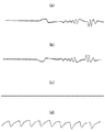
- Embodiment 5 of the broadband sensor of the present invention (a) is an output signal of the first piezoelectric element, (b) is an output signal of the second piezoelectric element, and (c) is an output signal of the first piezoelectric element and the second piezoelectric element. A signal obtained by taking a difference from the output signal of the element, and (d) shows a signal obtained by amplifying the signal shown in (c).
- FIG. 1 is sectional drawing which shows Embodiment 1 of the wideband sensor of this invention.
- the insulating substrate 1 has a certain degree of rigidity and is difficult to deform.
- the piezoelectric element 2 is mounted almost at the center.
- piezoelectric ceramic is used as the piezoelectric element 2.
- a + electrode and a ⁇ electrode are formed, and when a vibration composed of a sound wave or a pulse wave is applied to the piezoelectric element 2, a voltage difference corresponding to the vibration is generated between the + electrode and the ⁇ electrode. It is configured as follows. This voltage difference can be extracted as a detection signal of the piezoelectric element 2.
- the piezoelectric element 2 when compared with a condenser microphone, the piezoelectric element 2 has a wide frequency characteristic from a very low range to a wide range and has a small size of 1/10 or less because there is no decrease in amplitude even in a very low range. can do.
- the power consumption is significantly low, and there is no moving part, so it has durability.
- the surface of the insulating substrate 1 has a cylindrical member 3 made of an enclosing member that is attached so as to surround the piezoelectric element 2, and the cylindrical member 3 has an end portion (hereinafter referred to as “the insulating substrate 1”). (Referred to as the front end portion), the end surface portion 4 is formed with an opening 4A through which the piezoelectric element 2 is exposed.
- the piezoelectric element 2 has a sound wave or wind to be detected. Etc. can enter through the opening 4A, and other unnecessary factors can be shielded by the end face portion 4, so that reliable detection can be performed.
- signals that can be taken out from the + and-poles of the piezoelectric element 2 are connected to the impedance conversion circuit 5, and the output from the impedance conversion circuit 5 is taken out as a detection signal of the piezoelectric element 2.
- the impedance conversion circuit 5 is configured to measure a signal from the piezoelectric element 2 with a circuit having a high impedance and output the voltage as a circuit having a low impedance. As a result, even if the input impedance after the next stage is low, the signal can be sufficiently transmitted.
- FIG. 1B is a diagram showing another example of the broadband sensor shown in the first embodiment of FIG.
- the piezoelectric element 2 is formed in the shape of a diaphragm, and the diaphragm type piezoelectric element 2 ′ configured in this way has its periphery insulated through the support base 1A. This is because it can be attached to the substrate 1.
- the broadband sensor configured as described above has an effect of enabling reliable detection because the sensitivity of the diaphragm type piezoelectric element 2 ′ is good.
- the broadband sensors of the second and subsequent embodiments include the piezoelectric elements 2 and 2A, respectively.
- the piezoelectric elements 2 and 2A may be configured as diaphragm type piezoelectric elements.
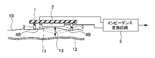
- FIG. 2 is a cross-sectional view showing Embodiment 2 of the broadband sensor of the present invention.
- the broadband sensor shown in FIG. 2 is a broadband sensor used in contact with the body surface.
- FIG. 2 is a diagram drawn in association with FIG. 1A, and the configuration different from the broadband sensor shown in FIG.
- the opening 4B having the same inner diameter as the inner diameter of the cylindrical member 3 is provided without having (indicated by reference numeral 4 in FIG. 1A).
- the broadband sensor configured as described above is used, for example, in such a manner that the tip of the cylindrical member 3 is brought into contact with the body surface 10 to form a sealed cavity 11 in the cylindrical member 3.
- a pulse wave 13 conducted from, for example, blood vessels (arteries, capillaries, etc.) 12 below the body surface 10 can be detected via the piezoelectric element 2 in the sealed cavity 11. Since the sealed cavity 11 around the piezoelectric element 2 can detect the pulse wave 13 from the body surface 10 with high sensitivity as a change in the air pressure in the cavity to the piezoelectric element 2, the piezoelectric element 2 can detect the pulse wave 13 with high sensitivity. There is an effect that can be detected.
- the cylindrical member 3 since the cylindrical member 3 has a function of forming the sealed cavity 11 around the piezoelectric element 2, it may be configured by, for example, an O-ring instead of the cylindrical member 3.
- the diameter of the O-ring needs to be larger than the height of the piezoelectric element 2. This is because when the tip of the O-ring is brought into contact with the body surface, a sealed cavity needs to be formed around the piezoelectric element 2 in the O-ring.
- FIG. 3 is a sectional view showing Embodiment 3 of the broadband sensor of the present invention.
- the broadband sensor shown in FIG. 3 is obtained by adding a disturbance noise removing configuration to the broadband sensor shown in FIG.
- a piezoelectric element 2 (hereinafter sometimes referred to as the first piezoelectric element 2) is mounted at substantially the center of the surface of the insulating substrate 1. ing.
- the surface of the insulating substrate 1 has a cylindrical member 3 attached so as to surround the first piezoelectric element 2, and this cylindrical member 3 attaches the first piezoelectric element 2 to the tip portion of the insulating substrate 1. It is configured to have an end surface portion 4 in which an opening 4A to be exposed is formed.
- a signal that can be extracted from the + pole and the ⁇ pole of the first piezoelectric element 2 is connected to an impedance conversion circuit 5 (hereinafter sometimes referred to as the first impedance conversion circuit 5).
- the second piezoelectric element 2A is further mounted substantially at the center of the back surface of the insulating substrate 1. Further, a cover member 6 is attached to the back surface of the insulating substrate 1 so as to surround the second piezoelectric element 2A and close the second piezoelectric element 2A. Signals that can be extracted from the + and ⁇ poles of the second piezoelectric element 2A are connected to the second impedance conversion circuit 5A. Further, the output of the first impedance conversion circuit 5 and the output of the second impedance conversion circuit 5A are input to the arithmetic circuit 7, and the arithmetic circuit 7 outputs the output of the first impedance conversion circuit 5 and the output of the second impedance conversion circuit 5A. The calculation result is taken out as an output of the calculation circuit 7.
- the first piezoelectric element 2 detects a sound wave or wind vibration to be detected and vibration due to disturbance noise
- the second piezoelectric element 2A has only vibration due to disturbance noise. Can be detected.
- the disturbance noise for example, vibration of the insulating substrate 1 can be considered.
- the first piezoelectric element 2 detects the vibration of the sound wave or wind to be detected and the vibration of the insulating substrate 1, whereas the second piezoelectric element 2A detects the vibration of the leading edge substrate 1. It becomes like this. This is because the second piezoelectric element 2A is blocked by the insulating substrate 1 and the cover member 6 and is in a state in which it is difficult to detect the sound wave and wind vibration.
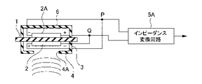
- FIG. 4 is a cross-sectional view showing Embodiment 4 of the broadband sensor of the present invention.
- the broadband sensor shown in FIG. 4 has a configuration drawn in association with FIG. In FIG.
- the configuration different from that in FIG. 3 is that the wirings drawn from the + pole and the ⁇ pole of the first piezoelectric element 2 are drawn from the ⁇ pole and the + pole of the second piezoelectric element 2A, respectively. This is because the difference between the output of the first piezoelectric element 2 and the output of the second piezoelectric element 2A is taken by connecting to each wiring. Then, a signal obtained at a connection point P between the positive pole of the first piezoelectric element 2 and the negative pole of the second piezoelectric element 2A, and a connection point Q between the negative pole of the first piezoelectric element 2 and the positive pole of the second piezoelectric element 2A. In other words, the signal obtained in the above step is taken out through the impedance conversion circuit 5.
- FIG. 5 is a sectional view showing Embodiment 5 of the wideband sensor of the present invention.
- the broadband sensor shown in FIG. 5 is obtained by adding a disturbance noise removing configuration to the broadband sensor shown in FIG.
- a piezoelectric element 2 (hereinafter sometimes referred to as a first piezoelectric element 2) is mounted almost at the center of the surface of the insulating substrate 1.
- the surface of the insulating substrate 1 has a cylindrical member 3 attached so as to surround the first piezoelectric element 2, and this cylindrical member 3 has an end surface (see FIGS. 1A and 1B) at the tip. ), An opening 4B having the same inner diameter as the inner diameter of the cylindrical member 3 is provided.
- a signal that can be extracted from the + pole and the ⁇ pole of the first piezoelectric element 2 is connected to an impedance conversion circuit 5 (hereinafter sometimes referred to as the first impedance conversion circuit 5).
- the second piezoelectric element 2A is further mounted substantially at the center of the back surface of the insulating substrate 1. Further, a cover member 6 is attached to the back surface of the insulating substrate 1 so as to surround the second piezoelectric element 2A and close the second piezoelectric element 2A. Signals that can be extracted from the + and ⁇ poles of the second piezoelectric element 2A are connected to the second impedance conversion circuit 5A. Further, the output of the first impedance conversion circuit 5 and the output of the second impedance conversion circuit 5A are input to the arithmetic circuit 7, and the arithmetic circuit 7 outputs the output of the first impedance conversion circuit 5 and the output of the second impedance conversion circuit 5A. The calculation result is taken out as an output of the calculation circuit 7.
- the first piezoelectric element 2 detects a pulse wave signal to be detected and a signal due to disturbance noise
- the second piezoelectric element 2A detects only a signal due to disturbance. Therefore, as described above, by calculating the difference between the output of the first impedance conversion circuit 5 and the output of the second impedance conversion circuit 5A by the arithmetic circuit 7, only the signal to be detected can be extracted. become. For this reason, the signal to be detected can be taken out without disturbance noise, and reliable detection can be performed.
- FIG. 7A is a diagram showing an output signal of the first piezoelectric element 2.
- the output signal of the first piezoelectric element 2 is taken out as a signal including a pulse wave signal and a signal due to disturbance noise.
- FIG. 7B is a diagram showing an output signal of the second piezoelectric element 2A.
- the output signal of the second piezoelectric element 2A is taken out as a signal with only disturbance noise.
- FIG. 7C is a diagram showing a signal obtained by taking the difference between the output signal of the first piezoelectric element 2 and the output signal of the second piezoelectric element 2A. It can be seen that the signal shown in FIG. 7C is extracted as a signal from which disturbance noise is removed.
- FIG.7 (d) shows the signal which amplified the signal shown in FIG.7 (c), and it becomes clear that it is a signal corresponding to a pulse wave.
- FIG. 6 is a sectional view showing Embodiment 6 of the wideband sensor of the present invention.
- FIG. 6 is a diagram drawn in association with FIG.
- the configuration different from that of FIG. 5 is that the wirings drawn from the + pole and the ⁇ pole of the first piezoelectric element 2 are drawn from the ⁇ pole and the + pole of the second piezoelectric element 2A, respectively. This is because the difference between the output of the first piezoelectric element 2 and the output of the second piezoelectric element 2A is taken by connecting to each wiring. Then, a signal obtained at a connection point P between the positive pole of the first piezoelectric element 2 and the negative pole of the second piezoelectric element 2A, and a connection point Q between the negative pole of the first piezoelectric element 2 and the positive pole of the second piezoelectric element 2A. In other words, the signal obtained in the above step is taken out through the impedance conversion circuit 5.
- the broadband sensor configured as described above has the same effect as that of the fifth embodiment, can eliminate the impedance conversion circuit 5 required in the fifth embodiment, and can reduce the number of impedance circuits.
- the second piezoelectric element 2A mounted on the insulating substrate 1 is closed by the cover member 6.
- the cover member 6 is not necessarily attached. Of course it is good.
- the second piezoelectric element 2A can be configured such that it can detect disturbance noise and cannot detect sound waves and pulse waves without attaching the cover member 6 described above.
- the signal from the piezoelectric element is output through the impedance conversion circuit.
- the present invention is not limited to this, and it is needless to say that an impedance conversion circuit including an amplifier circuit may be used, or an amplifier may be used instead of the impedance conversion circuit.
- FIG. 8 is an explanatory diagram showing another example of usage of the broadband sensor of the present invention.
- FIG. 8 shows a sash window 20 attached to a general house, for example, and is a view of the sash window 20 viewed from the indoor side.
- the sash window 20 is composed of, for example, two sash windows 20A and 20B, and these sash windows 20A and 20B each run along two rails (not shown) arranged in close proximity to each other. Windows are opened and closed.
- the sash windows 20A and 20B are disposed so as to be closed, and the frame body 21A on the sash window 20B side of the sash window 20A and the frame body 21B on the sash window 20A side of the sash window 20B are locked. Locked by member 22.
- the broadband sensor 30 is mounted on the frame body 21B close to the locking member 22 of the sash window 20B.
- the broadband sensor 30 functions as a security sensor for a thief or the like who tries to intrude by opening the sash window 20.
- FIG. 9 is a cross-sectional view showing a configuration of the broadband sensor 30. In FIG. 9, the broadband sensor 30 is shown as being attached to the frame body 21B of the sash window 20B.
- the broadband sensor 30 first includes a cylindrical casing 31, and has an opening end 31 ⁇ / b> A at one end of the casing 31 on the sash window 20 ⁇ / b> B side, and a hole coaxially with the casing 31 at the other end. It has the obstruction
- a cylindrical body 32 is inserted into the hole 31B of the casing 31, and the cylindrical body 32 is attached to the casing 31 by, for example, bonding an outer peripheral surface thereof to an inner peripheral surface of the hole 31B.
- An O-ring 33 arranged coaxially with the cylindrical body 32 is attached to one end of the cylindrical body 32 on the sash window 20B side. Thereby, the cylindrical body 32 functions as a support for attaching the O-ring 33 to the casing 31.
- the O-ring 33 is made of, for example, a rubber material having elasticity.
- the circuit board 34 is disposed so as to be substantially flush with, for example, the closing surface 31 ⁇ / b> C of the casing 31, and the outer peripheral surface of the circuit board 34 is the cylindrical body 32.
- the circuit board 34 is attached to the cylindrical body 32 by being bonded to the inner peripheral surface.
- a piezoelectric element 35 is mounted on the surface of the circuit board 34 on the sash window 20B side.
- a wireless transmitter 36 formed of, for example, a semiconductor chip is mounted on the surface of the circuit board 34 opposite to the mounting surface of the piezoelectric element 35.
- the wireless transmitter 36 is configured to transmit the output from the piezoelectric element 35 to a receiver (indicated by reference numeral 40 in FIG. 10) remotely disposed with respect to the broadband sensor 30 by radio waves.
- the receiver 10 will be described later.
- an air battery for driving the piezoelectric element 35 and the wireless receiver 36 is mounted on the circuit board 34.
- the broadband sensor 30 is configured such that the opening end 31A of the casing 31 on the sash window 20B side is fixed to the frame body 21B of the sash window 20 via the double-sided tape 37.
- the O-ring 33 supported by the cylindrical body 32 is brought into a relatively strong contact with the frame body 21B and is brought into close contact with the frame body 21B by the elastic force generated at that time.
- the portion surrounded by the circuit board 34, the cylindrical body 32, and the O-ring 33 forms a sealed cavity 39 together with the frame body 21 ⁇ / b> B of the sash window 20.
- the vibration conducted from the sash window 20 can be detected via the piezoelectric element 35 in the sealed cavity 39.
- the sealed cavity 39 around the piezoelectric element 35 can detect the vibration from the sash window 20 with high sensitivity to the piezoelectric element 35 as a change in air pressure in the sealed cavity 39, and the piezoelectric element 35 can detect the vibration with high sensitivity. Can do.
- FIG. 10 is an explanatory diagram showing a receiver 40 that receives radio waves transmitted from the wireless transmitter 36 of the wideband sensor 30.
- the receiver 40 is configured by, for example, a personal computer or a smart phone.
- the receiver 40 receives the radio wave (signal) from the wideband sensor 30 together with either the surface of the sash window 20 on which the broadband sensor 30 is attached or the surface opposite to the surface.
- a discrimination means 42 for discriminating whether an impact has been applied is provided.
- the receiver 40 receives the signal shown in FIG. In FIG. 11, a signal ⁇ received first corresponds to an impact signal applied from the outside of the sash window 20, and a signal ⁇ received next corresponds to an impact signal applied from the inside of the sash window 20. To do.
- FIG. 12A, 12B, and 12C are cross-sectional views exaggeratingly illustrating the deformation of the broadband sensor 30 that occurs with the sash window 20 in the series of processes described above.
- FIG. 12A shows the broadband sensor 30 when an impact is applied to the sash window 20 from the outside (in the direction of the arrow in the figure).
- the broadband sensor 30 has a concave outer side of the sash window 20 and an inner side of the sash window 20.
- the piezoelectric element 35 is deformed by being distorted so as to be convex, and the piezoelectric element 35 is also deformed accordingly, and the piezoelectric element 35 outputs a signal corresponding to this deformation.
- the signal from the piezoelectric element 35 obtained in this case is the signal ⁇ shown in FIG.
- the signal ⁇ is formed as a waveform having a large peak on the negative side, for example.
- transformation of the broadband sensor 30 shown to Fig.12 (a) comes to attenuate
- FIG. 12 (b) shows the broadband sensor 30 in a slight time lapse after impact from the outside of the sash window 20, and the broadband sensor 30 has a normal shape without distortion. There is no signal from the piezoelectric element 35 obtained in this case, and it corresponds to the period between the signal ⁇ and the signal ⁇ in FIG.
- FIG. 12 (c) shows the broadband sensor 30 when an impact is applied to the sash window 20 from the inside (in the direction of the arrow in the figure).
- the piezoelectric element 35 is also deformed by being distorted so as to be concave, and the piezoelectric element 35 outputs a signal corresponding to this deformation.
- the signal from the piezoelectric element 35 obtained in this case is the signal ⁇ shown in FIG.
- the signal ⁇ is formed as a waveform having a large peak on the positive side, for example. Then, when the impact from the inside of the sash window 20 is eliminated, the deformation shown in FIG. 12C is attenuated.
- the discrimination circuit 42 of the receiver 40 discriminates between the signal ⁇ and the signal ⁇ by discriminating the waveform difference between the signal ⁇ and the signal ⁇ .
- the receiver 40 is provided with a warning means 43.
- the warning means 43 issues a warning.
- there are various methods for warning but for example, it is performed by voice through a speaker or the like.
- the warning means 43 issues a warning because the sash window 20 is subjected to an impact from the outside. This is because it is determined that there are thieves or the like trying to invade.
- a shock is applied to the sash window 20 from the inside, it is assumed that, for example, children including babies are hitting the sash window 20 and at least a thief or the like sashes from the inside. Based on the rule of thumb that the window 20 will not be impacted.
- the broadband sensor 30 that functions as a security sensor is attached to a window, for example.
- the present invention is not limited to windows and may be attached to doors or other building members.
- the broadband sensor 30 may be configured as follows in order to firmly and easily attach the broadband sensor 30 to the building member. .
- FIG. 13 is a cross-sectional view of the broadband sensor 30 ′ drawn in association with FIG. 9, for example, being attached to a door.
- the structure different from the case of FIG. 9 is that the door 38 is made of a magnetic material made of, for example, iron.
- casing 31 'of broadband sensor 30' is comprised with the magnet.
- the cylindrical body 32, the O-ring 33, the circuit board 34, the piezoelectric element 35, the wireless transmitter 36, and the like have the same configuration as in FIG.
- the opening end 31 ⁇ / b> A on the door 38 side of the casing 31 ′ made of magnet is attracted to the door 38, which is a magnetic body, by magnetic force.
- the O-ring 33 supported by the cylindrical body 32 comes into relatively strong contact with the door 38 and comes into close contact with the door 38 due to the elasticity generated at that time.
- a portion surrounded by the circuit board 34, the cylindrical body 32, and the O-ring 33 forms a sealed cavity 39 together with the door 38.
- the broadband sensor 30 ′ configured as described above can be firmly and easily attached to any part of a building member made of, for example, iron, and can be used in the same manner as shown in the ninth embodiment. become able to.
- the broadband sensor shown in any of the above may be used.
- the broadband sensor has an O-ring (corresponding to the O-ring 33 in FIGS. 9 and 13) and a wireless transmitter (wireless in FIGS. 9 and 13) in the configuration shown in the first to eighth embodiments.
- the transmitter 36 may be configured as necessary.
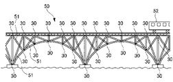
- FIG. 14 is an explanatory diagram showing another example of usage of the broadband sensor of the present invention.
- FIG. 14 is a diagram showing an iron bridge 50 having a so-called truss structure.
- the broadband sensor 30 is each attached to the some location which this iron bridge 50 requires.
- the broadband sensor 30 shown in FIG. 9 (or FIG. 13) is used.
- the diagonal member 51 of the truss-structured iron bridge 50 is likely to be corroded, and the broadband sensor 30 is intended to detect a change in rigidity and mass of the material 51 caused by deterioration and damage. That is, vibration is applied to the iron bridge 50, and the output from the piezoelectric element (indicated by reference numeral 35 in FIG. 9) of the broadband sensor 30 is obtained corresponding to the rigidity and mass of the material to which the broadband sensor 30 is attached. The deterioration and damage of the material over time can be analyzed.
- vibrations can be applied to the iron bridge 50 by the traveling of the bridge inspection vehicle 52 that moves along the iron bridge 50, and the piezoelectric element (indicated by reference numeral 35 in FIG. 9) of the broadband sensor 30 caused by this vibration. Is transmitted to a receiver composed of, for example, a personal computer mounted on the bridge inspection vehicle 52 via a wireless transmitter (indicated by reference numeral 36 in FIG. 9).
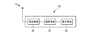
- FIG. 15 shows a receiver 53 mounted on the bridge inspection vehicle 52, which receiver 53 receives a signal from a wireless transmitter (indicated by reference numeral 36 in FIG.
- An analysis unit 55 that performs vibration analysis of the iron bridge 50 based on a signal from the reception unit 54 and a display unit 56 that displays an analysis result obtained by the analysis unit 55 as necessary are configured.
- an inspector is on the bridge inspection vehicle 52, and the inspector collects and analyzes output information of the piezoelectric element (indicated by reference numeral 35 in FIG. 9) through the receiver 54.
- the broadband sensor 30 of the present invention is attached to a civil structure such as a bridge 50, and the vibration of the civil structure is analyzed.
- the present invention is not limited to this.
- it may be attached to a building such as a building and the vibration of the building may be analyzed.
- the broadband sensor 30 (or 30 ′) and the receiver 53 may be referred to as a broadband sensor device.
- Embodiment 12 In the eleventh embodiment, an example using the broadband sensor shown in FIG. 9 and FIG. 13 is shown.
- the present invention is not limited to this, and any one of the first to eighth embodiments is shown. Needless to say, a wideband sensor may be used.
- the broadband sensor has an O-ring (corresponding to the O-ring 33 in FIGS. 9 and 13) and a wireless transmitter (wireless in FIGS. 9 and 13) in the configuration shown in the first to eighth embodiments.
- the transmitter 36 may be configured as necessary.
- SYMBOLS 1 Insulating substrate, 1A ... Support stand, 2 ... Piezoelectric element (1st piezoelectric element), 2A ... 2nd piezoelectric element, 2 '... Diaphragm type piezoelectric element, 3 ... Cylindrical member, 4 ... ... end face part, 4A, 4B ... opening, 5 ... impedance conversion circuit (first impedance conversion circuit), 5A ... second impedance conversion circuit, 6 ... cover member, 7 ... arithmetic circuit, 10 ... body Table, 11 ... Sealed cavity, 12 ... Blood vessel, 13 ... Pulse wave, 20, 20A, 20B ... Sash window, 21A, 21B ... Frame, 22 ...
Landscapes
- Engineering & Computer Science (AREA)
- Physics & Mathematics (AREA)
- Aviation & Aerospace Engineering (AREA)
- General Physics & Mathematics (AREA)
- Acoustics & Sound (AREA)
- Signal Processing (AREA)
- Bridges Or Land Bridges (AREA)
- Measuring Fluid Pressure (AREA)
- Measuring Pulse, Heart Rate, Blood Pressure Or Blood Flow (AREA)
- Measurement Of Mechanical Vibrations Or Ultrasonic Waves (AREA)
Description
本発明は広帯域センサに関する。
たとえば、車両の運転者の単位時間当たりの心拍数、あるいは呼吸数などを検出することによって、運転者の覚醒度を推定するようにし、車両の安全走行を支援するようにする技術が知られている。
下記特許文献1には、このような運転者の心拍数を検知する心拍検出装置が開示されている。該心拍検出装置は、人体の心拍に応じて振動する第1振動板と、該第1振動板に対向配置され該第1振動板の振動に応じて該第1振動板と異なる振動特性で振動する第2振動板と、該第1振動板と第2振動板の間のキャビティの形状を維持する形状維持部材とを備え、気道を介して該キャビティ内の空気の振動をコンデンサマイクのダイアフラムに伝動させるように構成されている。
また、本発明に関連する従来の技術としては、たとえば、下記特許文献2、3に示すものが知られている。特許文献2には、脈波に応じて振動する振動膜と、該振動膜の外周部を固定する枠部と、該振動膜の中央部を複数に仕切る仕切り部と、この仕切り部によって仕切られた各振動膜に配置され該振動膜の信号を検知するセンサ素子と、を備えた脈波測定装置が開示されている。また、特許文献3には、体表に装着できるフレキシブルシートに超音波素子をアレイ状に搭載した脈波測定シートを構成し、該脈波測定シートを橈骨動脈付近の手首に貼り、橈骨動脈に対して正しく当てられた超音波素子の信号だけを読み取るようにすることによって、細かな位置合わせを不要としたものが開示されている。
しかし、上述した特許文献1に示す技術は、キャビティ内の空気の振動をダイアフラムを介してコンデンサマイクで検知するようにしたものである。この場合、コンデンサマイクは、比較的狭い周波数帯域を有し、サイズも大きく、消費電力も大きいという不都合を有していた。また、ダイアフラム、振動膜を用いることによって構成を複雑にしているという不都合を有していた。
また、特許文献2に示す技術は、センサ素子として圧電素子等を用いることも記載されているが、振動膜を用い、この振動膜を固定する枠部等を必要とするため、構成が複雑になるという不都合を有していた。
さらに、特許文献3に示す技術は、脈波を測定するものとして記載されているが、該脈波を検知する手段として超音波素子を用い、該超音波素子は体表に装着するフレキシブルシートに搭載された構成となっているものである。このため、超音波素子は、体表とフレキシブルシートを介して当接され、該フレキシブルシートによって脈波の超音波素子への伝導が充分でなくなるという不都合を有していた。
本発明は、このような事情に基づいてなされたものであり、その目的は、簡単な構成にも拘わらず、音波、脈波等を効率よく検知し得る広帯域センサを提供することにある。
また、本発明の他の目的は、音波、脈波等を検知する際に外乱ノイズを取り入れることなく検知し得る広帯域センサを提供することにある。
このような目的を達成するために、本発明の広帯域センサは、絶縁基板に搭載した圧電素子を囲み、少なくとも該圧電素子と対向する部分に開口を有する囲い部材(たとえば筒状部材)を設けることによって、前記開口を通して伝導される該圧電素子の周辺の空気振動を該圧電素子が検知する構成としたものである。これにより、広帯域センサの囲い部材の開口を検知する対象に向けることにより、該対象から発する音波、脈波等は、該開口を通して圧電素子の周辺の空気を振動させ、この振動を該圧電素子が効率よく検知できるようにすることができる。そして、上述のような構成は、振動膜、ダイアフラム等を用いていない構造となっているため、極めて簡単に構成することができるようになる。
また、音波、脈波等を検知する前記圧電素子(第1圧電素子と称する)とは別個の他の圧電素子(第2圧電素子と称する)を前記絶縁基板に搭載させ、該他の圧電素子によって、検知しようとする音波、脈波以外の外乱ノイズのみを検知できる構成にし、第1圧電素子の出力信号と第2圧電素子の出力信号との差分をとるようにしたものである。これにより、第1圧電素子において、検出しようとする音波、脈波等に外乱ノイズが含まれていても、該外乱ノイズを除去できるようになる。
本発明は、以下の構成によって把握できる。
(1)本発明の広帯域センサは、絶縁基板と、前記絶縁基板の表面に搭載された圧電素子と、前記絶縁基板の前記表面に前記圧電素子を囲んで取付けられて開口を有する囲い部材と、前記圧電素子の出力を取り出す出力手段と、を備えることを特徴とする。
(2)本発明の広帯域センサは、(1)の構成において、前記広帯域センサは、体表に当接させて用いられ、前記体表に前記囲い部材の前記開口を当接させ、前記囲い部材内に密閉キャビティを形成して用いることを特徴とする。
(3)本発明の広帯域センサは、(1)、(2)のいずれかの構成において、前記圧電素子の出力を取り出す前記出力手段は、インピーダンス変換回路あるいは増幅回路であることを特徴とする。
(4)本発明の広帯域センサは、(3)の構成において、前記インピーダンス変換回路は増幅回路を含むことを特徴とする。
(5)本発明の広帯域センサは、(1)ないし(4)のいずれかの構成において、 前記第1圧電素子からの出力を取り出す第1出力手段と、前記絶縁基板の裏面に搭載された第2圧電素子と、前記第2圧電素子からの出力を取り出す第2出力手段と、前記第2手段の出力値と前記第1手段の出力値の差分を取り出す第3出力手段と、を備えることを特徴する。
(6)本発明の広帯域センサは、(4)の構成において、前記絶縁基板の前記裏面には、前記第2圧電素子を閉塞するカバー部材が備えられていることを特徴とする。
(7)本発明の広帯域センサは、(6)の構成において、前記カバー部材はピンホールが形成されていることを特徴とする請求項6に記載の広帯域センサ。
(8)本発明の広帯域センサは、(2)ないし(6)の構成において、体表に当接させて用いられ、前記体表に前記囲い部材の前記開口を当接させ、前記囲い部材内に密閉キャビティを形成して用いることを特徴とする請求項2ないし請求項7のいずれかに記載の広帯域センサ。
(9)本発明の広帯域センサは、(5)ないし(8)の構成において、前記第1圧電素子の+極、-極からの各出力を第1インピーダンス変換回路に入力させることにより前記第1出力手段を構成し、前記第2圧電素子の+極、-極からの各出力を第2インピーダンス変換回路に入力させることにより前記第2出力手段を構成するとともに、前記第1インピーダンス変換回路の出力および前記第2インピーダンス変換回路の出力を演算回路に入力させることで前記第3出力手段を構成することを特徴とする。
(10)本発明の広帯域センサは、(5)ないし(8)の構成において、前記第1圧電素子の+極、-極から引き出された前記第1出力手段としての各配線を、それぞれ、前記第2圧電素子の-極、+極から引き出された前記第2出力手段としての各配線に接続することにより前記第3出力手段を構成することを特徴とする。
(11)本発明の広帯域センサは、(1)ないし(10)のいずれかの広帯域センサであって、建築物に取り付けられることを特徴とする。
(12)本発明の広帯域センサ装置は、広帯域センサと、前記広帯域センサの出力を受信する受信器とを備え、前記広帯域センサは、(1)ないし(10)のいずれかの広帯域センサからなるとともに、建築部材に取り付けられ、前記受信器は、前記建築部材の前記広帯域センサを取り付けた側の面あるいは前記面と反対側の面のいずれかから衝撃が加わったかを判別する判別手段が具備されていることを特徴とする。
(13)本発明の広帯域センサは、(12)の構成において、前記建築部材は窓であることを特徴とする。
(14)本発明の広帯域センサは、(1)ないし(10)のいずれかの広帯域センサであって、土木構造物に取り付けられることを特徴とする。
(15)本発明の広帯域センサは、(14)の構成において、前記土木構造物は橋梁であることを特徴とする。
(16)本発明の広帯域センサ装置は、広帯域センサと、前記広帯域センサの出力を受信する受信器とを備え、前記広帯域センサは、(1)ないし(10)のいずれかの広帯域センサからなるともに、土木構造物に取り付けられ、前記受信器は、前記土木構造物に加えられた振動に基づく前記広帯域センサの出力を解析する解析手段が具備されていることを特徴とする。
(17)本発明の広帯域センサは、(1)ないし(16)のいずれかの広帯域センサであって、その出力手段からの出力を遠隔配置された受信器に電波で送信するワイヤレス送信器を備えることを特徴とする。
(1)本発明の広帯域センサは、絶縁基板と、前記絶縁基板の表面に搭載された圧電素子と、前記絶縁基板の前記表面に前記圧電素子を囲んで取付けられて開口を有する囲い部材と、前記圧電素子の出力を取り出す出力手段と、を備えることを特徴とする。
(2)本発明の広帯域センサは、(1)の構成において、前記広帯域センサは、体表に当接させて用いられ、前記体表に前記囲い部材の前記開口を当接させ、前記囲い部材内に密閉キャビティを形成して用いることを特徴とする。
(3)本発明の広帯域センサは、(1)、(2)のいずれかの構成において、前記圧電素子の出力を取り出す前記出力手段は、インピーダンス変換回路あるいは増幅回路であることを特徴とする。
(4)本発明の広帯域センサは、(3)の構成において、前記インピーダンス変換回路は増幅回路を含むことを特徴とする。
(5)本発明の広帯域センサは、(1)ないし(4)のいずれかの構成において、 前記第1圧電素子からの出力を取り出す第1出力手段と、前記絶縁基板の裏面に搭載された第2圧電素子と、前記第2圧電素子からの出力を取り出す第2出力手段と、前記第2手段の出力値と前記第1手段の出力値の差分を取り出す第3出力手段と、を備えることを特徴する。
(6)本発明の広帯域センサは、(4)の構成において、前記絶縁基板の前記裏面には、前記第2圧電素子を閉塞するカバー部材が備えられていることを特徴とする。
(7)本発明の広帯域センサは、(6)の構成において、前記カバー部材はピンホールが形成されていることを特徴とする請求項6に記載の広帯域センサ。
(8)本発明の広帯域センサは、(2)ないし(6)の構成において、体表に当接させて用いられ、前記体表に前記囲い部材の前記開口を当接させ、前記囲い部材内に密閉キャビティを形成して用いることを特徴とする請求項2ないし請求項7のいずれかに記載の広帯域センサ。
(9)本発明の広帯域センサは、(5)ないし(8)の構成において、前記第1圧電素子の+極、-極からの各出力を第1インピーダンス変換回路に入力させることにより前記第1出力手段を構成し、前記第2圧電素子の+極、-極からの各出力を第2インピーダンス変換回路に入力させることにより前記第2出力手段を構成するとともに、前記第1インピーダンス変換回路の出力および前記第2インピーダンス変換回路の出力を演算回路に入力させることで前記第3出力手段を構成することを特徴とする。
(10)本発明の広帯域センサは、(5)ないし(8)の構成において、前記第1圧電素子の+極、-極から引き出された前記第1出力手段としての各配線を、それぞれ、前記第2圧電素子の-極、+極から引き出された前記第2出力手段としての各配線に接続することにより前記第3出力手段を構成することを特徴とする。
(11)本発明の広帯域センサは、(1)ないし(10)のいずれかの広帯域センサであって、建築物に取り付けられることを特徴とする。
(12)本発明の広帯域センサ装置は、広帯域センサと、前記広帯域センサの出力を受信する受信器とを備え、前記広帯域センサは、(1)ないし(10)のいずれかの広帯域センサからなるとともに、建築部材に取り付けられ、前記受信器は、前記建築部材の前記広帯域センサを取り付けた側の面あるいは前記面と反対側の面のいずれかから衝撃が加わったかを判別する判別手段が具備されていることを特徴とする。
(13)本発明の広帯域センサは、(12)の構成において、前記建築部材は窓であることを特徴とする。
(14)本発明の広帯域センサは、(1)ないし(10)のいずれかの広帯域センサであって、土木構造物に取り付けられることを特徴とする。
(15)本発明の広帯域センサは、(14)の構成において、前記土木構造物は橋梁であることを特徴とする。
(16)本発明の広帯域センサ装置は、広帯域センサと、前記広帯域センサの出力を受信する受信器とを備え、前記広帯域センサは、(1)ないし(10)のいずれかの広帯域センサからなるともに、土木構造物に取り付けられ、前記受信器は、前記土木構造物に加えられた振動に基づく前記広帯域センサの出力を解析する解析手段が具備されていることを特徴とする。
(17)本発明の広帯域センサは、(1)ないし(16)のいずれかの広帯域センサであって、その出力手段からの出力を遠隔配置された受信器に電波で送信するワイヤレス送信器を備えることを特徴とする。
このように構成された広帯域センサによれば、簡単な構成にも拘わらず、音波、脈波等を効率よく検知することができるようになる。また、音波、脈波等を検知する際に外乱ノイズを取り入れることなく検知することができるようになる。
以下、添付図面を参照して、本発明を実施するための形態(以下、実施形態)について詳細に説明する。なお、実施形態の説明の全体を通して同じ要素には同じ番号を付している。
(実施形態1)
図1(a)は、本発明の広帯域センサの実施形態1を示す断面図である。図1において、まず、絶縁基板1がある。絶縁基板1はある程度の剛性を有し、変形し難く形成されている。絶縁基板1の一方の面(表面と称す)には、そのほぼ中央に圧電素子2が搭載されている。この圧電素子2としては、たとえば圧電セラミックスが用いられている。圧電素子2は、+電極および-電極が形成され、圧電素子2に音波あるいは脈波等からなる振動が与えられた際、該+電極および-電極の間に該振動に応じた電圧差が生じるように構成されている。そして、この電圧差は圧電素子2の検知信号として取り出せるようになっている。
(実施形態1)
図1(a)は、本発明の広帯域センサの実施形態1を示す断面図である。図1において、まず、絶縁基板1がある。絶縁基板1はある程度の剛性を有し、変形し難く形成されている。絶縁基板1の一方の面(表面と称す)には、そのほぼ中央に圧電素子2が搭載されている。この圧電素子2としては、たとえば圧電セラミックスが用いられている。圧電素子2は、+電極および-電極が形成され、圧電素子2に音波あるいは脈波等からなる振動が与えられた際、該+電極および-電極の間に該振動に応じた電圧差が生じるように構成されている。そして、この電圧差は圧電素子2の検知信号として取り出せるようになっている。
ここで、圧電素子2は、たとえばコンデンサマイクロフォンと比較した場合、超低域でも振幅の減少が無いため、超低域から広域までの広い周波数特性を有し、サイズも1/10以下と小さく構成することができる。また、消費電力も大幅に低く、可動部分がないため耐久性を有する。
また、絶縁基板1の表面には、圧電素子2を囲んで取り付けられる囲い部材からなる筒状部材3を有し、この筒状部材3は、前記絶縁基板1と反対側の端部(以下、先端部と称する)において、圧電素子2を露出させる開口4Aが形成された端面部4を有するように構成されている。
このように筒状部材3の端部に端面部4を形成し、この端面部4に圧電素子2を露出させる開口4Aを形成することによって、圧電素子2には、検知しようとする音波あるいは風等のみが該開口4Aを通して入射でき、他の不要な要因を前記端面部4によって遮蔽できることから、信頼性ある検出を行うことができる。
さらに、圧電素子2の+極、-極から取り出せる信号は、インピーダンス変換回路5に接続され、該インピーダンス変換回路5からの出力を圧電素子2の検出信号として取り出すようになっている。
ここで、インピーダンス変換回路5は、圧電素子2からの信号を高いインピーダンスを持った回路で計測し、その電圧を低いインピーダンスを持った回路として出力してやるように構成されている。これにより、次の段以降の入力インピーダンスが低くても信号を充分に伝えることができる効果を奏するようになっている。
図1(b)は、図1(a)の実施形態1で示した広帯域センサの他の実施例を示した図である。
図1(a)の場合と比較して異なる構成は、圧電素子2をダイアフラムの形状に構成し、このように構成されたダイアフラム型圧電素子2’は、その周縁を支持台1Aを介して絶縁基板1に取り付けられるようにしたことにある。このように構成した広帯域センサは、ダイアフラム型圧電素子2’の感度が良好となることから、信頼性ある検知を行うことができる効果を奏する。
なお、実施形態2以降の他の実施形態の広帯域センサにおいて、それぞれ圧電素子2、2Aを備えるが、これら圧電素子2、2Aは、ダイアフラム型圧電素子として構成してもよいことはもちろんである。
(実施形態2)
図2は、本発明の広帯域センサの実施形態2を示す断面図である。図2に示す広帯域センサは、体表に当接させて用いられる広帯域センサを示している。
(実施形態2)
図2は、本発明の広帯域センサの実施形態2を示す断面図である。図2に示す広帯域センサは、体表に当接させて用いられる広帯域センサを示している。
図2は、図1(a)に対応付けて描いた図であり、図1(a)に示した広帯域センサと比べて異なる構成は、広帯域センサの筒状部材3において、先端部に端面部(図1(a)にて符号4で示す)を有することなく、筒状部材3の内径と同一の内径を有する開口4Bが設けられていることにある。
このように構成された広帯域センサは、たとえば、その筒状部材3の先端部を体表10に当接させ、該筒状部材3内に密閉キャビティ11を形成するようにして用いられる。この場合、体表10下のたとえば血管(動脈、毛細血管等)12から伝導される脈波13が、密閉キャビティ11内の圧電素子2を介して検知できるようになっている。圧電素子2の周辺の密閉キャビティ11は、体表10からの脈波13を該圧電素子2にキャビティ内の空気圧変化として高感度に検出できることから、圧電素子2は該脈波13を高感度に検出することができる効果を奏する。
上述したように、筒状部材3は、圧電素子2の周辺に密閉キャビティ11を構成する機能を有することから、該筒状部材3に替え、たとえばOリングで構成するようにしてもよい。この場合、Oリングの直径は、圧電素子2の高さよりも大きいことが必要となる。Oリングの先端部を体表に当接させた場合に、Oリング内の圧電素子2の周辺に密閉キャビティが構成される必要があるからである。
なお、図2において、圧電素子2が絶縁基板1に搭載されていること、圧電素子2の+電極、-電極からの信号がインピーダンス変換回路5を介して取り出されることは、図1(a)、(b)で示したと同様である。
(実施形態3)
図3は、本発明の広帯域センサの実施形態3を示す断面図である。図3に示す広帯域センサは、図1(a)に示した広帯域センサに外乱ノイズ除去用の構成を付加させたものとなっている。
(実施形態3)
図3は、本発明の広帯域センサの実施形態3を示す断面図である。図3に示す広帯域センサは、図1(a)に示した広帯域センサに外乱ノイズ除去用の構成を付加させたものとなっている。
図3に示す広帯域センサは、まず、図1(a)の場合と同様に、絶縁基板1の表面のほぼ中央に圧電素子2(以下、第1圧電素子2と称する場合がある)が搭載されている。また、絶縁基板1の表面には、第1圧電素子2を囲んで取り付けられる筒状部材3を有し、この筒状部材3は、前記絶縁基板1の先端部において、第1圧電素子2を露出させる開口4Aが形成された端面部4を有するように構成されている。そして、第1圧電素子2の+極、-極から取り出せる信号は、インピーダンス変換回路5(以下、第1インピーダンス変換回路5と称する場合がある)に接続されている。
そして、実施形態3の広帯域センサは、さらに、絶縁基板1の裏面のほぼ中央に第2圧電素子2Aが搭載されている。また、絶縁基板1の裏面には、第2圧電素子2Aを囲むとともに該第2圧電素子2Aを閉塞して形成されたカバー部材6が取り付けられている。そして、第2圧電素子2Aの+極、-極から取り出せる信号は、第2インピーダンス変換回路5Aに接続されている。さらに、第1インピーダンス変換回路5の出力および第2インピーダンス変換回路5Aの出力を演算回路7に入力させ、該演算回路7では、第1インピーダンス変換回路5の出力と第2インピーダンス変換回路5Aの出力の差分をとるようになっており、その演算結果を該演算回路7の出力として取り出すようになっている。
このように構成された広帯域センサにおいて、第1圧電素子2は、検知しようとする音波や風の振動と外乱ノイズによる振動を検出するのに対し、第2圧電素子2Aは、外乱ノイズによる振動のみを検出することができる。ここで、外乱ノイズとしては、たとえば絶縁基板1の振動が考えられる。この場合、第1圧電素子2は、検知しようとする音波や風の振動と絶縁基板1の前記振動を検出してしまうのに対し、第2圧電素子2Aは前縁基板1の振動を検出するようになる。第2圧電素子2Aは絶縁基板1およびカバー部材6によって閉塞され、前記音波や風の振動を検出し難い状態となっているからである。したがって、上述のように、演算回路7によって、第1インピーダンス変換回路5の出力と第2インピーダンス変換回路5Aの出力の差分をとることにより、検知しょうとする信号のみを取り出すことができるようになる。このため、検知しようとする信号を外乱ノイズなく取り出すことができ、信頼性ある検知を行うことができる。
なお、カバー部材6は、必ずしも密閉構造とする必要はなく、たとえば該カバー部材6にピンホール等が形成されていてもよい。そして、このような構成は、後に説明する実施形態4ないし実施形態6においても採用されてもよいことはもちろんである。
(実施形態4)
図4は、本発明の広帯域センサの実施形態4を示す断面図である。図4に示す広帯域センサは、図3に対応づけて描いた構成となっている。図4において、図3の場合と比較して異なる構成は、第1圧電素子2の+極、-極から引き出された各配線を、それぞれ、第2圧電素子2Aの-極、+極から引き出された各配線に接続することにより、第1圧電素子2の出力と第2圧電素子2Aの出力の差分をとるようにしたことにある。そして、第1圧電素子2の+極と第2圧電素子2Aの-極の接続点Pで得られる信号、および第1圧電素子2の-極と第2圧電素子2Aの+極の接続点Qで得られる信号をインピーダンス変換回路5を介して取り出すようにしたことにある。
なお、カバー部材6は、必ずしも密閉構造とする必要はなく、たとえば該カバー部材6にピンホール等が形成されていてもよい。そして、このような構成は、後に説明する実施形態4ないし実施形態6においても採用されてもよいことはもちろんである。
(実施形態4)
図4は、本発明の広帯域センサの実施形態4を示す断面図である。図4に示す広帯域センサは、図3に対応づけて描いた構成となっている。図4において、図3の場合と比較して異なる構成は、第1圧電素子2の+極、-極から引き出された各配線を、それぞれ、第2圧電素子2Aの-極、+極から引き出された各配線に接続することにより、第1圧電素子2の出力と第2圧電素子2Aの出力の差分をとるようにしたことにある。そして、第1圧電素子2の+極と第2圧電素子2Aの-極の接続点Pで得られる信号、および第1圧電素子2の-極と第2圧電素子2Aの+極の接続点Qで得られる信号をインピーダンス変換回路5を介して取り出すようにしたことにある。
このように構成した広帯域センサは、実施形態3と同様の効果を奏するとともに、実施形態3で必要としたインピーダンス変換回路5を不要とでき、インピーダンス回路の数を減らすことができるようになる。
(実施形態5)
図5は、本発明の広帯域センサの実施形態5を示す断面図である。図5に示す広帯域センサは、図2に示した広帯域センサに外乱ノイズ除去用の構成を付加させたものとなっている。
(実施形態5)
図5は、本発明の広帯域センサの実施形態5を示す断面図である。図5に示す広帯域センサは、図2に示した広帯域センサに外乱ノイズ除去用の構成を付加させたものとなっている。
図5に示す広帯域センサは、まず、図2の場合と同様に、絶縁基板1の表面のほぼ中央に圧電素子2(以下、第1圧電素子2と称する場合がある)が搭載されている。また、絶縁基板1の表面には、第1圧電素子2を囲んで取り付けられる筒状部材3を有し、この筒状部材3は、その先端部に端面部(図1(a)、(b)にて符号4で示す)を有することなく、筒状部材3の内径と同一の内径を有する開口4Bが設けられていることにある。そして、第1圧電素子2の+極、-極から取り出せる信号は、インピーダンス変換回路5(以下、第1インピーダンス変換回路5と称する場合がある)に接続されている。
そして、実施形態3の広帯域センサは、さらに、絶縁基板1の裏面のほぼ中央に第2圧電素子2Aが搭載されている。また、絶縁基板1の裏面には、第2圧電素子2Aを囲むとともに該第2圧電素子2Aを閉塞して形成されたカバー部材6が取り付けられている。そして、第2圧電素子2Aの+極、-極から取り出せる信号は、第2インピーダンス変換回路5Aに接続されている。さらに、第1インピーダンス変換回路5の出力および第2インピーダンス変換回路5Aの出力を演算回路7に入力させ、該演算回路7では、第1インピーダンス変換回路5の出力と第2インピーダンス変換回路5Aの出力の差分をとるようになっており、その演算結果を該演算回路7の出力として取り出すようになっている。
このように構成した広帯域センサにおいても、第1圧電素子2は、検知しようとする脈波の信号と外乱ノイズによる信号を検出するのに対し、第2圧電素子2Aは、外乱による信号のみを検出することから、上述のように、演算回路7によって、第1インピーダンス変換回路5の出力と第2インピーダンス変換回路5Aの出力の差分をとることにより、検知しようとする信号のみを取り出すことができるようになる。このため、検知しようとする信号を外乱ノイズなく取り出すことができ、信頼性ある検知を行うことができる。
なお、図7(a)は、第1圧電素子2の出力信号を示す図である。第1圧電素子2の出力信号は、脈波の信号と外乱ノイズによる信号とが含まれた信号として取り出される。図7(b)は、第2圧電素子2Aの出力信号を示す図である。第2圧電素子2Aの出力信号は、外乱ノイズのみの信号として取り出される。図7(c)は、第1圧電素子2の出力信号と第2圧電素子2Aの出力信号の差分をとった信号を示す図である。図7(c)に示す信号は、外乱ノイズが除去された信号して取り出されていることが判明する。なお、図7(d)は、図7(c)に示す信号を増幅した信号を示し、脈波に対応する信号となっていることが明らかとなる。
(実施形態6)
図6は、本発明の広帯域センサの実施形態6を示す断面図である。図6は、図5と対応づけて描いた図となっている。
(実施形態6)
図6は、本発明の広帯域センサの実施形態6を示す断面図である。図6は、図5と対応づけて描いた図となっている。
図6において、図5の場合と比較して異なる構成は、第1圧電素子2の+極、-極から引き出された各配線を、それぞれ、第2圧電素子2Aの-極、+極から引き出された各配線に接続することにより、第1圧電素子2の出力と第2圧電素子2Aの出力の差分をとるようにしたことにある。そして、第1圧電素子2の+極と第2圧電素子2Aの-極の接続点Pで得られる信号、および第1圧電素子2の-極と第2圧電素子2Aの+極の接続点Qで得られる信号をインピーダンス変換回路5を介して取り出すようにしたことにある。
このように構成した広帯域センサは、実施形態5と同様の効果を奏するとともに、実施形態5で必要としたインピーダンス変換回路5を不要とでき、インピーダンス回路の数を減らすことができるようになる。
(実施形態7)
実施形態3ないし実施形態6のそれぞれにおいて、絶縁基板1に搭載された第2圧電素子2Aは、カバー部材6によって閉塞された状態としたものあるが、必ずしも、該カバー部材6は取り付けなくてもよいことはもちろんである。特に、上述したカバー部材6を取り付けなくても、第2圧電素子2Aは、外乱ノイズを検知でき、音波、脈波を検知できないように構成することができるからである。
(実施形態8)
上述した各実施形態では、圧電素子からの信号をインピーダンス変換回路を経て出力させるようにしている。しかし、これに限定されることはなく、増幅回路を具備するインピーダンス変換回路であっても、また、インピーダンス変換回路の代わりに増幅器を用いるようにしてもよいことはもちろんである。
(実施形態7)
実施形態3ないし実施形態6のそれぞれにおいて、絶縁基板1に搭載された第2圧電素子2Aは、カバー部材6によって閉塞された状態としたものあるが、必ずしも、該カバー部材6は取り付けなくてもよいことはもちろんである。特に、上述したカバー部材6を取り付けなくても、第2圧電素子2Aは、外乱ノイズを検知でき、音波、脈波を検知できないように構成することができるからである。
(実施形態8)
上述した各実施形態では、圧電素子からの信号をインピーダンス変換回路を経て出力させるようにしている。しかし、これに限定されることはなく、増幅回路を具備するインピーダンス変換回路であっても、また、インピーダンス変換回路の代わりに増幅器を用いるようにしてもよいことはもちろんである。
以上、説明したことから明らかなように、本発明の広帯域センサによれば、簡単な構成にも拘わらず、音波、脈波等を効率よく検知することができるようになる。また、音波、脈波等を検知する際に外乱ノイズを取り入れることなく検知することができるようになる。
(実施形態9)
図8は、本発明の広帯域センサの使用態様の他の例を示す説明図である。
図8は、たとえば一般家屋に取り付けられるサッシ窓20を示し、屋内側から該サッシ窓20を観た図となっている。
サッシ窓20はたとえば2つのサッシ窓20A、20Bから構成され、これらサッシ窓20A、20Bは、それぞれ、近接して平行配置された2つの各レール(図示せず)に沿って走行するようにして窓の開閉がなされるようになっている。
(実施形態9)
図8は、本発明の広帯域センサの使用態様の他の例を示す説明図である。
図8は、たとえば一般家屋に取り付けられるサッシ窓20を示し、屋内側から該サッシ窓20を観た図となっている。
サッシ窓20はたとえば2つのサッシ窓20A、20Bから構成され、これらサッシ窓20A、20Bは、それぞれ、近接して平行配置された2つの各レール(図示せず)に沿って走行するようにして窓の開閉がなされるようになっている。
図8は、各サッシ窓20A、20Bが閉状態となるように配置されており、サッシ窓20Aのサッシ窓20B側の枠体21Aとサッシ窓20Bのサッシ窓20A側の枠体21Bは係止部材22によってロックされている。そして、たとえばサッシ窓20Bの前記係止部材22に近接する枠体21B上に広帯域センサ30が取り付けられている。
この広帯域センサ30は、サッシ窓20を抉じ開けて侵入しようとする泥棒等に対する防犯センサとして機能するようになっている。
図9は、前記広帯域センサ30の構成を示す断面図である。図9では、該広帯域センサ30はサッシ窓20Bの枠体21Bに取り付けられた状態として示している。
図9は、前記広帯域センサ30の構成を示す断面図である。図9では、該広帯域センサ30はサッシ窓20Bの枠体21Bに取り付けられた状態として示している。
図9に示すように、広帯域センサ30は、まず、筒状のケーシング31を備え、このケーシング31のサッシ窓20B側の一端に開口端31Aを有し、他端に該ケーシング31と同軸に孔31Bが形成された閉塞面31Cを有する。
ケーシング31の前記孔31Bには筒状体32が挿入され、該筒状体32は、その外周面が前記孔31Bの内周面にたとえば接着されることによって該ケーシング31に取り付けられている。筒状体32のサッシ窓20B側の一端には該筒状体32と同軸に配置されるO-リング33が取り付けられている。これにより、筒状体32はO-リング33をケーシング31に取り付けるための支持体として機能するようになっている。なお、O-リング33は弾性を有するたとえばゴム材で構成されている。
また、筒状体32には、その内部において、回路基板34がたとえばケーシング31の閉塞面31Cとほぼ面一になるように配置され、該回路基板34は、その外周面が筒状体32の内周面にたとえば接着されることによって該筒状体32に取り付けられている。
回路基板34のサッシ窓20B側の表面には圧電素子35が搭載されている。また、回路基板34の該圧電素子35の搭載面と反対側の面には、たとえば半導体チップによって構成されるワイヤレス送信器36が搭載されている。このワイヤレス送信器36は、圧電素子35からの出力を、当該広帯域センサ30に対して遠隔配置された受信器(図10において符号40で示す)に電波で送信するように構成されている。この受信器10については後に説明する。なお、回路基板34には、図示していないが、圧電素子35、ワイヤレス受信器36を駆動させるたとえば空気電池が搭載されている。
そして、図9に戻り、広帯域センサ30は、ケーシング31のサッシ窓20B側の開口端31Aが両面テープ37を介してサッシ窓20の枠体21Bに固着されるようになっている。この場合、筒状体32に支持されたO-リング33は、前記枠体21Bに比較的強く当接され、その際に生じる弾力によって前記枠体21Bに密着されるようになっている。これにより、回路基板34、筒状体32、O-リング33とで囲まれる部分は、サッシ窓20の枠体21Bとともに、密閉キャビティ39を構成するようになる。
この場合、サッシ窓20から伝導される振動が、密閉キャビティ39内の圧電素子35を介して検知できるようになっている。圧電素子35の周辺の密閉キャビティ39は、サッシ窓20からの振動を該圧電素子35に密閉キャビティ39内の空気圧変化として高感度に検出でき、圧電素子35は該振動を高感度に検出することができる。
図10は、広帯域センサ30のワイヤレス送信器36から送信された電波を受信する受信器40を示す説明図である。この受信器40は、たとえばパーソナルコンピュータあるいはスマートフォーン等で構成されるようになっている。
この場合、受信器40は、広帯域センサ30からの電波(信号)を受信する受信手段41とともにサッシ窓20の該広帯域センサ30を取り付けた側の面あるいは前記面と反対側の面のいずれかから衝撃が加わったかを判別する判別手段42が備えられたものとなっている。
この場合、受信器40は、広帯域センサ30からの電波(信号)を受信する受信手段41とともにサッシ窓20の該広帯域センサ30を取り付けた側の面あるいは前記面と反対側の面のいずれかから衝撃が加わったかを判別する判別手段42が備えられたものとなっている。
すなわち、サッシ窓20に外側から衝撃を加え、若干の時間経過の後に、サッシ窓20に内側から衝撃を加えた場合を想定する。この場合、受信器40には、広帯域センサ30から図11に示す信号を受けるようになる。図11において、最初に受信する信号αは、サッシ窓20の外側から加えられた衝撃の信号に相当し、次に受信する信号βは、サッシ窓20の内側から加えられた衝撃の信号に相当する。
図12(a)、(b)、(c)は、上述の一連の過程においてサッシ窓20とともに生じる広帯域センサ30の変形を誇張して描いた断面図である。
図12(a)は、サッシ窓20に外側(図中矢印方向)から衝撃を加えた場合の広帯域センサ30を示し、広帯域センサ30は、サッシ窓20の外側が凹にサッシ窓20の内側が凸となるように歪んで変形し、圧電素子35もこれに応じた変形がなされ、この変形に対応する信号を圧電素子35は出力するようになる。この場合において得られる圧電素子35からの信号は、図11に示す信号αとなっている。信号αは、たとえば負側に大きなピークを有する波形として形成されている。そして、サッシ窓20の外側からの衝撃がなくなった場合、図12(a)に示す広帯域センサ30の変形は、減衰するようになる。
図12(a)は、サッシ窓20に外側(図中矢印方向)から衝撃を加えた場合の広帯域センサ30を示し、広帯域センサ30は、サッシ窓20の外側が凹にサッシ窓20の内側が凸となるように歪んで変形し、圧電素子35もこれに応じた変形がなされ、この変形に対応する信号を圧電素子35は出力するようになる。この場合において得られる圧電素子35からの信号は、図11に示す信号αとなっている。信号αは、たとえば負側に大きなピークを有する波形として形成されている。そして、サッシ窓20の外側からの衝撃がなくなった場合、図12(a)に示す広帯域センサ30の変形は、減衰するようになる。
図12(b)は、サッシ窓20の外側からの衝撃の後の若干の時間経過における広帯域センサ30を示し、広帯域センサ30は、歪みのない通常の形状になる。この場合において得られる圧電素子35からの信号は無く、図11において信号αと信号βとの間の期間に相当するようになっている。
図12(c)は、サッシ窓20に内側(図中矢印方向)から衝撃を加えた場合の広帯域センサ30を示し、広帯域センサ30は、サッシ窓20の外側が凸にサッシ窓20の内側が凹となるように歪んで変形し、圧電素子35もこれに応じた変形がなされ、この変形に対応する信号を圧電素子35が出力するようになる。この場合において得られる圧電素子35からの信号は、図11に示す信号βとなっている。信号βは、たとえば正側に大きなピークを有する波形として形成されている。そして、サッシ窓20の内側からの衝撃がなくなった場合、図12(c)に示す変形は減衰するようになる。
そして、図10に戻り、受信器40の判別回路42は、信号αおよび信号βの波形の相違を識別することによって信号αであるか信号βであるかを判別するようになっている。そして、受信器40は、警告手段43を具備し、判別回路42によって信号αを判別した場合に、該警告手段43によって警告を発するようになっている。ここで、警告としては、種々の方法があるが、たとえば、スピーカを通した音声等によって行う。
ここで、判別手段42が信号αを判別した際に、警告手段43によって警告を発するようにしたのは、サッシ窓20に外側から衝撃が加わっていることから、該サッシ窓20を抉じ開けて侵入しようとする泥棒等がいると判断されるからである。これに対し、サッシ窓20に内側から衝撃が加わった場合に警告を発しないのは、たとえば赤子を含む子供達がサッシ窓20を叩いている場合等を想定でき、少なくとも泥棒等が内側からサッシ窓20に衝撃を与えることはないだろうという経験則に基づいている。
これにより、広帯域センサ30を取り付けた住人は、住居の外から侵入者が窓を抉じ開けているのではないかという注意が喚起されるようになり、該広帯域センサ30を防犯センサとして機能させることができる。
なお、この明細書において、広帯域センサ30(あるいは30’)と受信器40を広帯域センサ装置と称する場合がある。
(実施形態10)
実施形態9では、防犯センサとして機能させる広帯域センサ30は、たとえば窓に取り付けたものである。しかし、窓に限定されることなく、ドア、あるいは他の建築部材に取り付けるようにしてもよいことはもちろんである。
なお、この明細書において、広帯域センサ30(あるいは30’)と受信器40を広帯域センサ装置と称する場合がある。
(実施形態10)
実施形態9では、防犯センサとして機能させる広帯域センサ30は、たとえば窓に取り付けたものである。しかし、窓に限定されることなく、ドア、あるいは他の建築部材に取り付けるようにしてもよいことはもちろんである。
この場合、建築部材がたとえば鉄等の磁性体からなる場合、広帯域センサ30の該建築部材への取付けを強固・簡単に行うために、該広帯域センサ30を次に示すように構成してもよい。
図13は、図9に対応づけて描いた広帯域センサ30’の断面図であり、たとえばドアに取り付けられた状態で示している。
図13において、図9の場合と異なる構成は、まず、ドア38はたとえば鉄等からなる磁性体から構成されている。そして、広帯域センサ30’のケーシング31’は磁石によって構成されている。その他、たとえば、筒状体32、O-リング33、回路基板34、圧電素子35、ワイヤレス送信器36等は、図9の場合と同様の構成となっている。
図13において、図9の場合と異なる構成は、まず、ドア38はたとえば鉄等からなる磁性体から構成されている。そして、広帯域センサ30’のケーシング31’は磁石によって構成されている。その他、たとえば、筒状体32、O-リング33、回路基板34、圧電素子35、ワイヤレス送信器36等は、図9の場合と同様の構成となっている。
このように構成した広帯域センサ30’は、磁石からなるケーシング31’のドア38側の開口端31Aが磁性体であるドア38に磁力によって吸着されるようになる。この場合、筒状体32に支持されたO-リング33は、ドア38に比較的強く当接され、その際に生じる弾力によってドア38に密着されるようになる。これにより、回路基板34、筒状体32、O-リング33とで囲まれる部分は、ドア38とともに、密閉キャビティ39を構成するようになる。
このように構成した広帯域センサ30’は、たとえば鉄等からなる建築部材であれば、そのどこの部分においても強固に、かつ簡単に取付けることができ、実施形態9に示したと同様に用いることができるようになる。
なお、実施形態9、実施形態10では、それぞれ、図9、図13に示す広帯域センサを用いた例を示したものであるが、これに限定されることはなく、実施形態1ないし実施形態8のうちいずれかに示した広帯域センサを用いるようにしてもよいことはいうまでもない。この場合、広帯域センサは、実施形態1ないし実施形態8に示した構成に、O-リング(図9、図13のO-リング33に相当する)、ワイヤレス送信器(図9、図13のワイヤレス送信器36に相当する)を必要に応じて具備させた構成とするようにしてもよいことはもちろんである。
(実施形態11)
図14は、本発明の広帯域センサの使用態様の他の例を示す説明図である。
図14は、いわゆるトラス構造を有する鉄橋50を示した図である。そして、この鉄橋50の必要とする複数の箇所にそれぞれ広帯域センサ30が取り付けられている。この広帯域センサ30としては、たとえば図9(あるいは図13)に示したものが使用されている。トラス構造の鉄橋50の斜材51は腐食が生じ易く、その劣化や損傷がもたらす該材料51の剛性や質量の変化を、該広帯域センサ30によって検出しようとするものである。
すなわち、鉄橋50に振動を与え、これにともなう広帯域センサ30の圧電素子(図9において符号35で示す)からの出力が、該広帯域センサ30を取り付けた材料の剛性や質量に対応して得られ、該材料の経時的な劣化や損傷が解析できるようになっている。
図14は、本発明の広帯域センサの使用態様の他の例を示す説明図である。
図14は、いわゆるトラス構造を有する鉄橋50を示した図である。そして、この鉄橋50の必要とする複数の箇所にそれぞれ広帯域センサ30が取り付けられている。この広帯域センサ30としては、たとえば図9(あるいは図13)に示したものが使用されている。トラス構造の鉄橋50の斜材51は腐食が生じ易く、その劣化や損傷がもたらす該材料51の剛性や質量の変化を、該広帯域センサ30によって検出しようとするものである。
すなわち、鉄橋50に振動を与え、これにともなう広帯域センサ30の圧電素子(図9において符号35で示す)からの出力が、該広帯域センサ30を取り付けた材料の剛性や質量に対応して得られ、該材料の経時的な劣化や損傷が解析できるようになっている。
図14に示すように、鉄橋50に沿って移動する橋梁点検車52の走行によって、鉄橋50に振動を与えることができ、この振動による広帯域センサ30の圧電素子(図9において符号35で示す)からの出力が、ワイヤレス送信器(図9において符号36で示す)を介して該橋梁点検車52に搭載されたたとえばパーソナルコンピュータからなる受信器に送信されるようになっている。
図15は、橋梁点検車52に搭載される受信器53を示し、該受信器53は、広帯域センサ30のワイヤレス送信機(図9において符号36で示す)から信号を受信する受信手段54、この受信手段54からの信号によって鉄橋50の振動解析を行う解析手段55と、この解析手段55によって得られる解析結果を必要に応じて表示する表示手段56とを備えて構成されている。
橋梁点検車52にはたとえば点検者が搭乗しており、該点検者は前記受信器54を通して圧電素子(図9において符号35で示す)の出力情報を、収集・解析するようになっている。
図15は、橋梁点検車52に搭載される受信器53を示し、該受信器53は、広帯域センサ30のワイヤレス送信機(図9において符号36で示す)から信号を受信する受信手段54、この受信手段54からの信号によって鉄橋50の振動解析を行う解析手段55と、この解析手段55によって得られる解析結果を必要に応じて表示する表示手段56とを備えて構成されている。
橋梁点検車52にはたとえば点検者が搭乗しており、該点検者は前記受信器54を通して圧電素子(図9において符号35で示す)の出力情報を、収集・解析するようになっている。
なお、実施形態11では、本発明の広帯域センサ30を橋梁50等の土木構造体に取り付け、該土木構造体の振動の解析を行うようにしたものである。しかし、これに限定されることはなく、たとえばビル等の建築物に取り付け、該建築物の振動の解析を行うようにしてもよいことはもちろんである。
なお、この明細書において、広帯域センサ30(あるいは30’)と受信器53を広帯域センサ装置と称する場合がある。
(実施形態12)
実施形態11では、それぞれ、図9、図13に示す広帯域センサを用いた例を示したものであるが、これに限定されることはなく、実施形態1ないし実施形態8のうちいずれかに示した広帯域センサを用いるようにしてもよいことはいうまでもない。この場合、広帯域センサは、実施形態1ないし実施形態8に示した構成に、O-リング(図9、図13のO-リング33に相当する)、ワイヤレス送信器(図9、図13のワイヤレス送信器36に相当する)を必要に応じて具備させた構成とするようにしてもよいことはもちろんである。
なお、この明細書において、広帯域センサ30(あるいは30’)と受信器53を広帯域センサ装置と称する場合がある。
(実施形態12)
実施形態11では、それぞれ、図9、図13に示す広帯域センサを用いた例を示したものであるが、これに限定されることはなく、実施形態1ないし実施形態8のうちいずれかに示した広帯域センサを用いるようにしてもよいことはいうまでもない。この場合、広帯域センサは、実施形態1ないし実施形態8に示した構成に、O-リング(図9、図13のO-リング33に相当する)、ワイヤレス送信器(図9、図13のワイヤレス送信器36に相当する)を必要に応じて具備させた構成とするようにしてもよいことはもちろんである。
以上、実施形態を用いて本発明を説明したが、本発明の技術的範囲は上記実施形態に記載の範囲には限定されないことは言うまでもない。上記実施形態に、多様な変更または改良を加えることが可能であることが当業者に明らかである。また、その様な変更または改良を加えた形態も本発明の技術的範囲に含まれ得ることが、特許請求の範囲の記載から明らかである。
1……絶縁基板、1A……支持台、2……圧電素子(第1圧電素子)、2A……第2圧電素子、2’……ダイアフラム型圧電素子、3……筒状部材、4……端面部、4A、4B……開口、5……インピーダンス変換回路(第1インピーダンス変換回路)、5A……第2インピーダンス変換回路、6……カバー部材、7……演算回路、10……体表、11……密閉キャビティ、12……血管、13……脈波、20、20A、20B……サッシ窓、21A、21B……枠体、22……係止部材、30、30’……広帯域センサ、31、31’……ケーシング、31A……開口端、31B……孔、31C……閉塞面、32……筒状体、33……O-リング、34……回路基板、35……圧電素子、36……ワイヤレス送信器、37……両面テープ、38……ドア、39……密閉キャビティ、40……受信器、41……受信手段、42……判別手段、43……警告手段、50……鉄橋、51……斜材、52……橋梁点検車、53……受信器、54……受信手段、55……解析手段、56……表示手段。
Claims (17)
- 絶縁基板と、
前記絶縁基板の表面に搭載された圧電素子と、
前記絶縁基板の前記表面に前記圧電素子を囲んで取付けられ開口を有する囲い部材と、
前記圧電素子の出力を取り出す出力手段と、を備えることを特徴とする広帯域センサ。 - 前記広帯域センサは、体表に当接させて用いられ、前記体表に前記囲い部材の前記開口を当接させ、前記囲い部材内に密閉キャビティを形成して用いることを特徴とする請求項1に記載の広帯域センサ。
- 前記圧電素子の出力を取り出す前記出力手段は、インピーダンス変換回路あるいは増幅回路であることを特徴とする請求項1、2のいずれかに記載の広帯域センサ。
- 前記インピーダンス変換回路は増幅回路を含むことを特徴とする請求項3に記載の広帯域センサ。
- 前記第1圧電素子からの出力を取り出す第1出力手段と、前記絶縁基板の裏面に搭載された第2圧電素子と、前記第2圧電素子からの出力を取り出す第2出力手段と、前記第2出力手段の出力値と前記第1手段の出力値の差分を取り出す第3出力手段と、を備えることを特徴する請求項1ないし4のいずれかに記載の広帯域センサ。
- 前記絶縁基板の前記裏面には、前記第2圧電素子を閉塞するカバー部材が備えられていることを特徴とする請求項5に記載の広帯域センサ。
- 前記カバー部材はピンホールが形成されていることを特徴とする請求項6に記載の広帯域センサ。
- 前記広帯域センサは、体表に当接させて用いられ、前記体表に前記囲い部材の前記開口を当接させ、前記囲い部材内に密閉キャビティを形成して用いることを特徴とする請求項2ないし請求項7のいずれかに記載の広帯域センサ。
- 前記第1圧電素子の+極、-極からの各出力を第1インピーダンス変換回路に入力させることにより前記第1出力手段を構成し、前記第2圧電素子の+極、-極からの各出力を第2インピーダンス変換回路に入力させることにより前記第2出力手段を構成するとともに、前記第1インピーダンス変換回路の出力および前記第2インピーダンス変換回路の出力を演算回路に入力させることで前記第3出力手段を構成することを特徴とする請求項5ないし請求項8のいずれかに記載の広帯域センサ。
- 前記第1圧電素子の+極、-極から引き出された前記第1出力手段としての各配線を、それぞれ、前記第2圧電素子の-極、+極から引き出された前記第2出力手段としての各配線に接続することにより前記第3出力手段を構成することを特徴とする請求項5ないし請求項8のいずれかに記載の広帯域センサ。
- 請求項1ないし請求項10のいずれかの広帯域センサであって、建築物に取り付けられることを特徴とする広帯域センサ。
- 広帯域センサと、前記広帯域センサの出力を受信する受信器とを備え、
前記広帯域センサは、請求項1ないし請求項10のいずれかの広帯域センサからなるとともに、建築部材に取り付けられ、
前記受信器は、前記建築部材の前記広帯域センサを取り付けた側の面あるいは前記面と反対側の面のいずれかから衝撃が加わったかを判別する判別手段が具備されていることを特徴とする広帯域センサ装置。 - 前記建築部材は窓であることを特徴とする請求項12に記載の広帯域センサ装置。
- 請求項1ないし請求項10のいずれかの広帯域センサであって、土木構造物に取り付けられることを特徴とする広帯域センサ。
- 前記土木構造物は橋梁であることを特徴とする請求項14に記載の広帯域センサ。
- 広帯域センサと、前記広帯域センサの出力を受信する受信器とを備え、
前記広帯域センサは、請求項1ないし請求項10のいずれかの広帯域センサからなるともに、土木構造物に取り付けられ、
前記受信器は、前記土木構造物に加えられた振動に基づく前記広帯域センサの出力を解析する解析手段が具備されていることを特徴とする広帯域センサ装置。 - 請求項1ないし請求項16のいずれかの広帯域センサであって、その出力手段からの出力を遠隔配置された受信器に電波で送信するワイヤレス送信器を備えることを特徴とする広帯域センサ。
Priority Applications (1)
| Application Number | Priority Date | Filing Date | Title |
|---|---|---|---|
| JP2014507307A JP5899308B2 (ja) | 2012-03-29 | 2012-07-24 | 広帯域センサ |
Applications Claiming Priority (2)
| Application Number | Priority Date | Filing Date | Title |
|---|---|---|---|
| JP2012075378 | 2012-03-29 | ||
| JP2012-075378 | 2012-03-29 |
Publications (1)
| Publication Number | Publication Date |
|---|---|
| WO2013145352A1 true WO2013145352A1 (ja) | 2013-10-03 |
Family
ID=49258702
Family Applications (1)
| Application Number | Title | Priority Date | Filing Date |
|---|---|---|---|
| PCT/JP2012/068638 Ceased WO2013145352A1 (ja) | 2012-03-29 | 2012-07-24 | 広帯域センサ |
Country Status (2)
| Country | Link |
|---|---|
| JP (1) | JP5899308B2 (ja) |
| WO (1) | WO2013145352A1 (ja) |
Cited By (4)
| Publication number | Priority date | Publication date | Assignee | Title |
|---|---|---|---|---|
| JP2016063939A (ja) * | 2014-09-24 | 2016-04-28 | 株式会社アドバンテスト | 脈波センサユニット |
| WO2016167202A1 (ja) * | 2015-04-17 | 2016-10-20 | 太陽誘電株式会社 | 振動波形センサ及び波形解析装置 |
| JP2017196211A (ja) * | 2016-04-28 | 2017-11-02 | 太陽誘電株式会社 | 振動波形センサ |
| US11058310B2 (en) | 2014-09-24 | 2021-07-13 | Advantest Corporation | Pulse wave sensor unit |
Families Citing this family (2)
| Publication number | Priority date | Publication date | Assignee | Title |
|---|---|---|---|---|
| WO2018180289A1 (ja) | 2017-03-29 | 2018-10-04 | Tdk株式会社 | 流体圧力検出装置 |
| US11786134B2 (en) | 2017-03-29 | 2023-10-17 | Tdk Corporation | Fluid pressure detection device |
Citations (5)
| Publication number | Priority date | Publication date | Assignee | Title |
|---|---|---|---|---|
| JPH0835893A (ja) * | 1994-07-21 | 1996-02-06 | Omron Corp | 物理量センサ装置及び当該センサ装置を用いた機器 |
| JPH10197333A (ja) * | 1997-01-07 | 1998-07-31 | Sogo Keibi Hosho Co Ltd | ガラス破壊検出器 |
| JPH11355890A (ja) * | 1998-06-11 | 1999-12-24 | Murata Mfg Co Ltd | 圧電音響部品 |
| JP2003348695A (ja) * | 2002-05-30 | 2003-12-05 | Cti Science System Co Ltd | 媒質マイクロホン |
| JP2007142540A (ja) * | 2005-11-15 | 2007-06-07 | Nippon Telegr & Teleph Corp <Ntt> | 音響素子 |
Family Cites Families (4)
| Publication number | Priority date | Publication date | Assignee | Title |
|---|---|---|---|---|
| JP2644241B2 (ja) * | 1987-10-28 | 1997-08-25 | キヤノン株式会社 | 圧電体多層膜およびその製造方法 |
| JPH02227656A (ja) * | 1989-02-28 | 1990-09-10 | Showa Electric Wire & Cable Co Ltd | 部分放電検出装置 |
| JPH05290563A (ja) * | 1992-04-10 | 1993-11-05 | Fujitsu Ltd | 密閉構造 |
| JP2004032499A (ja) * | 2002-06-27 | 2004-01-29 | Nippon Telegr & Teleph Corp <Ntt> | 超音波センサ |
-
2012
- 2012-07-24 JP JP2014507307A patent/JP5899308B2/ja active Active
- 2012-07-24 WO PCT/JP2012/068638 patent/WO2013145352A1/ja not_active Ceased
Patent Citations (5)
| Publication number | Priority date | Publication date | Assignee | Title |
|---|---|---|---|---|
| JPH0835893A (ja) * | 1994-07-21 | 1996-02-06 | Omron Corp | 物理量センサ装置及び当該センサ装置を用いた機器 |
| JPH10197333A (ja) * | 1997-01-07 | 1998-07-31 | Sogo Keibi Hosho Co Ltd | ガラス破壊検出器 |
| JPH11355890A (ja) * | 1998-06-11 | 1999-12-24 | Murata Mfg Co Ltd | 圧電音響部品 |
| JP2003348695A (ja) * | 2002-05-30 | 2003-12-05 | Cti Science System Co Ltd | 媒質マイクロホン |
| JP2007142540A (ja) * | 2005-11-15 | 2007-06-07 | Nippon Telegr & Teleph Corp <Ntt> | 音響素子 |
Cited By (7)
| Publication number | Priority date | Publication date | Assignee | Title |
|---|---|---|---|---|
| JP2016063939A (ja) * | 2014-09-24 | 2016-04-28 | 株式会社アドバンテスト | 脈波センサユニット |
| US11058310B2 (en) | 2014-09-24 | 2021-07-13 | Advantest Corporation | Pulse wave sensor unit |
| WO2016167202A1 (ja) * | 2015-04-17 | 2016-10-20 | 太陽誘電株式会社 | 振動波形センサ及び波形解析装置 |
| CN107530006A (zh) * | 2015-04-17 | 2018-01-02 | 太阳诱电株式会社 | 振动波形传感器和波形分析装置 |
| JPWO2016167202A1 (ja) * | 2015-04-17 | 2018-02-08 | 太陽誘電株式会社 | 振動波形センサ及び波形解析装置 |
| US10842396B2 (en) | 2015-04-17 | 2020-11-24 | Taiyo Yuden Co., Ltd. | Vibration waveform sensor and waveform analysis device |
| JP2017196211A (ja) * | 2016-04-28 | 2017-11-02 | 太陽誘電株式会社 | 振動波形センサ |
Also Published As
| Publication number | Publication date |
|---|---|
| JPWO2013145352A1 (ja) | 2015-12-10 |
| JP5899308B2 (ja) | 2016-04-06 |
Similar Documents
| Publication | Publication Date | Title |
|---|---|---|
| JP5899308B2 (ja) | 広帯域センサ | |
| US10567896B2 (en) | Apparatus and methods for monitoring a microphone | |
| JP6085099B2 (ja) | 検体情報処理装置 | |
| US20120294119A1 (en) | Device for detecting acoustic waves and a system for locating a source of acoustic waves | |
| JP6107045B2 (ja) | 携帯情報端末 | |
| JP5614827B2 (ja) | 携帯電話端末及び健康状態監視システム | |
| WO2004025231A3 (en) | Acoustic sensing device, system and method for monitoring emissions from machinery | |
| GB2561021B (en) | Apparatus and methods for monitoring a microphone | |
| EP1519165A2 (en) | Piezoelectric vibration sensor | |
| US20170240418A1 (en) | Low-cost miniature mems vibration sensor | |
| CN110476440A (zh) | 用于监控麦克风的装置和方法 | |
| CN108030472A (zh) | 睡眠监测带 | |
| JP2000060845A (ja) | 生体音検出装置 | |
| ATE406492T1 (de) | Fenster- oder türolive | |
| JP2005078500A (ja) | ガラス破壊検出器 | |
| JP5896832B2 (ja) | 検体情報処理装置及び検体情報処理方法 | |
| JP7677821B2 (ja) | ヘッドセットシステム | |
| JP6027339B2 (ja) | 検体情報処理装置 | |
| JP5103882B2 (ja) | 心拍検出装置 | |
| JPH0737104U (ja) | 脈波検出装置 | |
| KR200412624Y1 (ko) | 진동 센서 | |
| JP2008039654A (ja) | 超音波を利用した振動センサ | |
| JP2002243539A (ja) | 振動検出器 | |
| RU132290U1 (ru) | Микрофонный датчик для снятия акустических колебаний с поверхности контролируемого объекта | |
| RU2447510C2 (ru) | Способ обнаружения часовых замедлителей и устройство для его осуществления |
Legal Events
| Date | Code | Title | Description |
|---|---|---|---|
| 121 | Ep: the epo has been informed by wipo that ep was designated in this application |
Ref document number: 12872354 Country of ref document: EP Kind code of ref document: A1 |
|
| ENP | Entry into the national phase |
Ref document number: 2014507307 Country of ref document: JP Kind code of ref document: A |
|
| NENP | Non-entry into the national phase |
Ref country code: DE |
|
| 122 | Ep: pct application non-entry in european phase |
Ref document number: 12872354 Country of ref document: EP Kind code of ref document: A1 |