WO2013145154A1 - 画像描画装置 - Google Patents
画像描画装置 Download PDFInfo
- Publication number
- WO2013145154A1 WO2013145154A1 PCT/JP2012/058138 JP2012058138W WO2013145154A1 WO 2013145154 A1 WO2013145154 A1 WO 2013145154A1 JP 2012058138 W JP2012058138 W JP 2012058138W WO 2013145154 A1 WO2013145154 A1 WO 2013145154A1
- Authority
- WO
- WIPO (PCT)
- Prior art keywords
- light
- optical axis
- light source
- axis deviation
- laser
- Prior art date
- Legal status (The legal status is an assumption and is not a legal conclusion. Google has not performed a legal analysis and makes no representation as to the accuracy of the status listed.)
- Ceased
Links
Images





Classifications
-
- G—PHYSICS
- G02—OPTICS
- G02B—OPTICAL ELEMENTS, SYSTEMS OR APPARATUS
- G02B26/00—Optical devices or arrangements for the control of light using movable or deformable optical elements
- G02B26/08—Optical devices or arrangements for the control of light using movable or deformable optical elements for controlling the direction of light
- G02B26/10—Scanning systems
- G02B26/105—Scanning systems with one or more pivoting mirrors or galvano-mirrors
Definitions
- the present invention relates to a technical field for detecting and correcting an optical axis shift.
- Patent Document 1 This type of technology is proposed in Patent Document 1, for example.
- Japanese Patent Application Laid-Open No. 2004-133620 proposes a technique for making a laser beam from a light source enter a light receiving element and detecting an optical axis shift based on an output signal of the light receiving element.
- Patent Document 1 proposes correcting an optical axis deviation by moving an optical element (a lens or a beam splitter) based on the detected optical axis deviation.
- Examples of the problem to be solved by the present invention include the above. It is an object of the present invention to provide an image drawing apparatus that can appropriately prevent light from being visually recognized when detecting an optical axis shift.
- the image drawing apparatus causes the drawing target to draw an image by scanning the first light source, the second light source, and the light emitted from the first light source and the second light source.
- Scanning means optical axis deviation detecting means for detecting deviation of an optical axis of light emitted from the first light source and the second light source and not scanned by the scanning means, and the first light source
- an optical axis correction unit that corrects the optical axis of the light emitted from the second light source to coincide with each other, and the first light source, the second light source, and the scanning unit during the detection operation by the optical axis deviation detection unit.
- a light shielding means for interrupting the optical path between the two.
- FIG. 1 shows a configuration of an image drawing apparatus according to a first embodiment.
- the structure of a light-receiving part is shown.
- the figure for demonstrating concretely the filter non-insertion state and filter insertion state which concern on 1st Example is shown.
- the figure for demonstrating the 1st control example of 1st Example is shown.
- the figure for demonstrating the 2nd control example of 1st Example is shown.
- the figure for demonstrating the 3rd control example of 1st Example is shown.
- the structure of the image drawing apparatus which concerns on 2nd Example is shown.
- the figure for demonstrating concretely the mirror insertion state and mirror non-insertion state which concern on 2nd Example is shown.
- the structure of the image drawing apparatus which concerns on 3rd Example is shown.
- the figure for demonstrating concretely the S polarization state and P polarization state which concern on 3rd Example is shown.
- an image drawing apparatus scans light emitted from a first light source, a second light source, the first light source, and the second light source, and draws an image on a drawing target.
- Means optical axis deviation detecting means for detecting an optical axis deviation of light emitted from the first light source and the second light source and not scanned by the scanning means, the first light source,
- An optical axis correction unit configured to correct the optical axes of the light emitted from the second light source, and the first light source, the second light source, and the scanning unit during a detection operation by the optical axis deviation detection unit;
- Light shielding means for blocking the optical path between the two.
- the image drawing apparatus detects a shift in the optical axis of the light emitted from the first light source and the second light source, and corrects the optical axes of the light emitted from the first light source and the second light source to coincide with each other.
- the light blocking means blocks the optical path between the first light source and the second light source and the scanning means during the detection operation by the optical axis deviation detecting means.
- the image drawing apparatus has an optical path to the scanning unit and an optical path to the optical axis deviation detecting unit, and blocks only the optical path to the scanning unit when detecting the optical axis deviation (optical axis). The optical path to the deviation detection means is not blocked).
- the deflection angle of the scanning means By the way, by controlling the deflection angle of the scanning means to be larger than that during normal operation, it is possible to suppress the light from being visually recognized at the time of detecting the optical axis deviation, but the control should be performed at an arbitrary timing. It is difficult.
- the image drawing apparatus blocks the optical path in front of the scanning unit, the image drawing apparatus can perform the blocking at an arbitrary timing.
- the light shielding unit is disposed in an optical path between the first light source and the second light source and the optical axis deviation detecting unit, and guides the light to the scanning unit.
- a control means for performing control to remove the light guide means from the optical path between the first light source and the second light source and the optical axis deviation detection means during the detection operation by the optical axis deviation detection means.
- the optical axis deviation when the optical axis deviation is not detected, light is incident only on the scanning means by the light guiding means, and no light is incident on the optical axis deviation detecting means.
- the light guide means is removed from the optical path, so that light is incident only on the optical axis deviation detection means, and no light is incident on the scanning means. Thereby, it can prevent appropriately that the light at the time of detection of optical axis deviation is visually recognized.
- the light from the first light source and the second light source is incident on one of the scanning unit and the optical axis deviation detecting unit without being divided, so that the light use efficiency is improved. It becomes possible to make it.
- the light shielding unit is disposed in an optical path between the first light source, the second light source, and the optical axis deviation detection unit, and has a predetermined polarization direction.
- a beam splitter that reflects light to the scanning means and allows light having a polarization direction other than the predetermined polarization direction to pass therethrough, and changes the polarization direction of the light from the first light source and the second light source, and changes the polarization direction.
- a liquid crystal element that emits light toward a beam splitter, and the liquid crystal so that light from the first light source and the second light source has a polarization direction other than the predetermined polarization direction at the time of detection operation by the optical axis deviation detection unit.
- Control means for controlling the element, and the optical axis deviation detecting means detects deviation of the optical axis of the light that has passed through the beam splitter.
- the liquid crystal element when the optical axis deviation is not detected, the liquid crystal element is controlled to emit light having a predetermined polarization direction, and the light emitted from the liquid crystal element is reflected by the beam splitter and scanned. Incident on the means.
- the liquid crystal element when the optical axis deviation is detected, the liquid crystal element is controlled so as to emit light having a polarization direction other than the predetermined polarization direction, and the light emitted from the liquid crystal element passes through the beam splitter. The light passes through and enters the optical axis deviation detecting means. In this case, no light is incident on the scanning means. Thereby, it can prevent appropriately that the light at the time of detection of optical axis deviation is visually recognized. Further, according to the image drawing apparatus described above, since the mechanical drive unit is not used, the apparatus can be reduced in size.
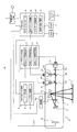
- FIG. 1 shows a configuration of an image drawing apparatus 1a according to the first embodiment.
- the image drawing apparatus 1a according to the first embodiment mainly includes an image signal input unit 2, a video ASIC 3, a frame memory 4, a ROM 5, a RAM 6, a laser driver ASIC 7, and a MEMS.
- the mirror control part 8, the laser light source unit 9a, and the control part 20a are provided.
- the image drawing device 1a is configured to be attachable to a head-up display for visually recognizing an image as a virtual image from the position (eye point) of the user, a user's head, and the like, and draws an image on the user's retina. Applies to head mounted displays.
- the image drawing apparatus 1a can be applied to a projector using laser light, for example.
- the laser light source unit 9a in FIG. 1 has shown the figure cut
- the image signal input unit 2 receives an image signal input from the outside and outputs it to the video ASIC 3.
- the video ASIC 3 is a block that controls the laser driver ASIC 7 and the MEMS mirror control unit 8 based on the image signal input from the image signal input unit 2 and the scanning position information input from the MEMS mirror 10, and is ASIC (Application Specific Integrated). Circuit).
- the video ASIC 3 includes a synchronization / image separation unit 31, a bit data conversion unit 32, a light emission pattern conversion unit 33, and a timing controller 34.
- the synchronization / image separation unit 31 separates the image data displayed on the image display unit and the synchronization signal from the image signal input from the image signal input unit 2 and writes the image data to the frame memory 4.
- the bit data converter 32 reads the image data written in the frame memory 4 and converts it into bit data.
- the light emission pattern conversion unit 33 converts the bit data converted by the bit data conversion unit 32 into a signal representing the light emission pattern of each laser.
- the timing controller 34 controls the operation timing of the synchronization / image separation unit 31 and the bit data conversion unit 32.
- the timing controller 34 also controls the operation timing of the MEMS mirror control unit 8 described later.
- the image data separated by the synchronization / image separation unit 31 is written.
- the ROM 5 stores a control program and data for operating the video ASIC 3. Various data are sequentially read from and written into the RAM 6 as a work memory when the video ASIC 3 operates.
- the laser driver ASIC 7 is a block that generates a signal for driving a laser diode (LD) provided in a laser light source unit 9a to be described later, and is configured as an ASIC.
- the laser driver ASIC 7 includes a red laser driving circuit 71, a blue laser driving circuit 72, and a green laser driving circuit 73.
- the red laser driving circuit 71 drives the red laser LD1 based on the signal output from the light emission pattern conversion unit 33.
- the blue laser drive circuit 72 drives the blue laser LD2 based on the signal output from the light emission pattern conversion unit 33.
- the green laser drive circuit 73 drives the green laser LD3 based on the signal output from the light emission pattern conversion unit 33.
- a MEMS (Micro Electro Mechanical Systems) mirror control unit 8 controls the MEMS mirror 10 based on a signal output from the timing controller 34.
- the MEMS mirror control unit 8 includes a servo circuit 81 and a driver circuit 82.
- the servo circuit 81 controls the operation of the MEMS mirror 10 based on a signal from the timing controller.
- the driver circuit 82 amplifies the control signal of the MEMS mirror 10 output from the servo circuit 81 to a predetermined level and outputs the amplified signal.
- the laser light source unit 9a mainly functions to emit laser light based on a drive signal output from the laser driver ASIC 7.
- the laser light source unit 9a includes a red laser LD1, a blue laser LD2, a green laser LD3, collimator lenses 91a, 91b, and 91c, dichroic mirrors 92a and 92b, a beam splitter 14, and a MEMS mirror 10. And a light receiving unit 13 and a movable filter 15.
- the red laser LD1 emits red laser light
- the blue laser LD2 emits blue laser light
- the green laser LD3 emits green laser light.
- the red laser LD1, the blue laser LD2, and the green laser LD3 are simply referred to as “laser LD”, and the red laser light, the blue laser light, and the green laser light are used without being distinguished from each other. In this case, it is simply expressed as “laser light”.
- the collimator lenses 91a, 91b, and 91c make the red laser light, the blue laser light, and the green laser light into parallel lights, respectively.
- the dichroic mirror 92a reflects the red laser light passing through the collimator lens 91a and transmits the green laser light passing through the collimator lens 91c.
- the dichroic mirror 92b transmits the red laser light and the green laser light that have passed through the dichroic mirror 92a, and reflects the blue laser light that has passed through the collimator lens 91b.
- the beam splitter 14 divides the laser light emitted from the dichroic mirror 92b in this way, reflects a part of the laser light toward the MEMS mirror 10, and transmits the remaining part of the laser light.
- the laser light transmitted through the beam splitter 14 is incident on the light receiving unit 13.
- the MEMS mirror 10 When the movable filter 15 is not located in the optical path between the beam splitter 14 and the MEMS mirror 10, the MEMS mirror 10 receives the laser beam reflected by the beam splitter 14 and directs the laser beam toward the screen 11. Reflect. Specifically, the MEMS mirror 10 operates to scan the screen 11 with a laser beam under the control of the MEMS mirror control unit 8 in order to display an image input to the image signal input unit 2, and Scan position information at that time (for example, information such as a mirror angle) is output to the video ASIC 3.
- the MEMS mirror 10 is an example of the “scanning unit” in the present invention.
- the screen 11 is an example of the “drawing object” in the present invention.
- the laser beam that has passed through the beam splitter 14 is incident on the light receiving unit 13.
- the light receiving unit 13 is a photoelectric conversion element (for example, a four-divided light receiving element) such as a photodetector, and outputs a light receiving signal Sd1 corresponding to the light receiving position of the laser light to the video ASIC 3.
- FIG. 2 is a view of the light receiving unit 13 observed from the direction of the arrow A1 in FIG.
- the light receiving unit 13 includes four light receiving elements 13a to 13b, and a spot SP corresponding to the laser light transmitted through the beam splitter 14 is formed.
- Each of the light receiving elements 13a to 13b outputs a signal corresponding to the area irradiated with the laser beam.
- the light receiving unit 13 subtracts the value obtained by adding the output value of the light receiving element 13b and the output value of the light receiving element 13d from the value obtained by adding the output value of the light receiving element 13a and the output value of the light receiving element 13c, An X deviation signal indicating the optical axis deviation in the direction (left and right direction) is output.
- the light receiving unit 13 subtracts the value obtained by adding the output value of the light receiving element 13c and the output value of the light receiving element 13d from the value obtained by adding the output value of the light receiving element 13a and the output value of the light receiving element 13b. , And output as a Y shift signal indicating the optical axis shift in the Y direction (vertical direction).
- the light receiving unit 13 outputs a signal including such an X deviation signal and a Y deviation signal to the video ASIC 3 as the above-described light reception signal Sd1.
- the video ASIC 3 detects the optical axis shift of the red laser LD1, the blue laser LD2, and the green laser LD3 based on the light reception signal Sd1 from the light receiving unit 13.
- the video ASIC 3 is based on the light reception signal Sd1 for each of the red laser light, the blue laser light, and the green laser light obtained when the red laser LD1, the blue laser LD2, and the green laser LD3 are individually emitted.
- the optical axis deviation for each laser LD is detected.
- the video ASIC 3 performs processing for correcting the optical axis deviation based on the detected optical axis deviation.
- the video ASIC 3 corrects the optical axis deviation by controlling the emission timing of the laser beam (that is, the modulation timing of the laser LD with respect to the movement of the MEMS mirror 10).
- the light receiving unit 13 corresponds to an example of the “optical axis deviation detecting unit” in the present invention
- the video ASIC 3 corresponds to an example of the “optical axis correcting unit” in the present invention.
- the movable filter 15 is configured to be able to block the passage of laser light (can be blocked). As the movable filter 15, various known filters can be applied. Further, the movable filter 15 is controlled between the position in the optical path between the beam splitter 14 and the MEMS mirror 10 and the position outside the optical path as indicated by an arrow A2 under the control of the control unit 20a. It is configured to be movable.
- FIG. 1 shows a state in which the movable filter 15 is disposed at a position off the optical path between the beam splitter 14 and the MEMS mirror 10 (hereinafter referred to as “filter non-insertion state”).
- filter non-insertion state a state where the movable filter 15 is disposed in the optical path between the beam splitter 14 and the MEMS mirror 10
- filter insertion state a state where the movable filter 15 is disposed in the optical path between the beam splitter 14 and the MEMS mirror 10 (hereinafter referred to as “filter insertion state”) is indicated by a broken line.
- the control unit 20a performs control to move the movable filter 15 via an actuator (not shown). Specifically, when the optical axis deviation is detected, the control unit 20a performs control to place the movable filter 15 at a position where the filter is inserted, and when the optical axis deviation is not detected. Performs control to arrange the movable filter 15 at a position where the filter is not inserted.
- the controller 20a controls the movable filter 15 based on a signal supplied from the video ASIC 3 and indicating whether or not to detect the optical axis deviation.
- the movable filter 15 and the control unit 20a correspond to an example of the “light shielding unit” in the present invention.
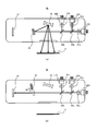
- FIG. 3 shows only the laser light source unit 9a.
- FIG. 3A shows a filter non-insertion state.
- the movable filter 15 is disposed at a position deviated from the optical path between the beam splitter 14 and the MEMS mirror 10.
- the laser light reflected by the beam splitter 14 is incident on the MEMS mirror 10, so that the laser light is irradiated on the screen 11 by the MEMS mirror 10, that is, an image is displayed.
- an image is displayed by setting in such a filter non-insertion state.
- FIG. 3B shows a filter insertion state.
- the filter insertion state is realized by moving the movable filter 15 as indicated by an arrow A3 from the position of the movable filter 15 in the filter non-insertion state shown in FIG.
- the movable filter 15 is disposed in the optical path between the beam splitter 14 and the MEMS mirror 10.
- the laser beam reflected by the beam splitter 14 is shielded by the movable filter 15 so that the laser beam is not incident on the MEMS mirror 10.
- the screen 11 is not irradiated with laser light, that is, no image is displayed.
- such a filter insertion state is set when an optical axis deviation is detected.
- the drive mechanism can be simplified and the cost can be reduced.
- the movable filter 15 is disposed in the optical path between the beam splitter 14 and the MEMS mirror 10 in the above. Instead, the movable filter 15 is disposed in the optical path between the MEMS mirror 10 and the screen 11. 15 may be arranged. This also prevents the laser light from reaching the screen 11 when detecting an optical axis shift. However, when the movable filter 15 is arranged in the optical path between the MEMS mirror 10 and the screen 11, the movable filter 15 is movable more than in the case where the movable filter 15 is arranged in the optical path between the beam splitter 14 and the MEMS mirror 10. It is necessary to increase the size of the filter 15.
- the movable filter 15 covers a relatively wide scanning range of the laser light. It is necessary to have. Therefore, from the viewpoint of miniaturization of the movable filter 15 and the like, the optical filter between the beam splitter 14 and the MEMS mirror 10 is disposed rather than the movable filter 15 disposed in the optical path between the MEMS mirror 10 and the screen 11. It can be said that it is preferable to dispose the movable filter 15.
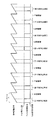
- FIG. 4 shows a first control example related to the control method according to the first embodiment.
- FIG. 4 shows a drive signal (vertical drive signal) for scanning the MEMS mirror 10 in the vertical direction and a control signal (filter control signal) for controlling the movable filter 15 used in the first control example.
- FIG. 4 shows a vertical drive signal timing chart on the upper side and a filter control signal timing chart on the lower side.
- the filter control signal is set to high level, the movable filter 15 is disposed at a position where the filter is inserted, and when the filter control signal is set to low level, the movable filter 15 is disposed at a position where the filter is not inserted. (The same shall apply hereinafter).
- one frame immediately after activation of the image drawing apparatus 1a is assigned to detection and correction of the optical axis deviation.
- the control unit 20a performs control to place the movable filter 15 at a position where the filter is inserted in a period corresponding to one frame immediately after activation.
- the MEMS mirror control unit 8 drives the MEMS mirror 10 by a so-called sawtooth wave using a vertical drive signal whose level increases with time (this control is performed for normal image display).
- the laser driver ASIC 7 performs control to individually emit the red laser LD1, the blue laser LD2, and the green laser LD3.
- the video ASIC 3 detects the optical axis deviation for each laser LD based on the light reception signal Sd1 of the light receiving unit 13 for each of the red laser light, the blue laser light, and the green laser light, and detects the detected light. Processing for correcting the optical axis deviation is performed based on the axis deviation.
- the control unit 20a places the movable filter 15 at a position where the filter is not inserted, and the video ASIC 3, the laser driver ASIC 7, and the MEMS mirror control unit 8 display an image to be presented to the user. Do normal control.
- the detection and correction of the optical axis deviation is not limited to being performed immediately after the activation, and the optical axis deviation may be detected and corrected at regular intervals after the activation.
- FIG. 5 shows a second control example related to the control method according to the first embodiment.
- FIG. 5 shows a timing chart of vertical drive signals used in the second control example on the upper side, and shows a timing chart of filter control signals used in the second control example on the lower side.
- a part of the period in each frame is assigned to the detection and correction of the optical axis deviation (in other periods, the detection is performed without detecting and correcting the optical axis deviation. Display the image that should be).
- an example of control when detecting and correcting the optical axis deviation will be mainly described.
- the control unit 20a performs control to place the movable filter 15 at a position where the filter is inserted in a partial period in each frame.
- the laser driver ASIC 7 performs control to emit only one laser LD of the red laser LD1, blue laser LD2, and green laser LD3, and the video ASIC 3
- the optical axis deviation for the laser LD is detected, and the optical axis deviation is detected based on the detected optical axis deviation. Processing for correction is performed.
- the MEMS mirror control unit 8 drives the MEMS mirror 10 in a sawtooth wave regardless of whether or not optical axis deviation is detected and corrected.
- the laser LD that detects and corrects the optical axis deviation is changed by changing the laser LD that emits light for each frame, and the optical axis deviation is detected and corrected in each frame.
- the timing to perform (that is, the temporal position for detecting and correcting the optical axis deviation within one frame) is changed.
- the first frame detects and corrects the optical axis deviation for the blue laser LD2 in the first predetermined period
- the second frame detects the optical axis deviation for the green laser LD3 in the middle period.
- the detection and correction of the optical axis deviation for the red laser LD1 is performed in the second half of the predetermined period, and the detection and correction of the optical axis deviation is not performed in the fourth frame. The same operation as in the first to fourth frames is repeated.
- the correction frequency of the optical axis deviation can be increased as compared with the first control example.
- the time required for detecting and correcting the optical axis deviation can be shortened, and no image is displayed. The period can be shortened.
- the timing at which no image is displayed in each frame changes by changing the timing for detecting and correcting the optical axis deviation in each frame (that is, the image is displayed in the image drawing area). The uncomfortable feeling given to the user can be suppressed.
- FIG. 6 shows a third control example related to the control method according to the first embodiment.
- FIG. 6 shows a timing chart of vertical drive signals used in the third control example on the upper side, and shows a timing chart of filter control signals used in the third control example on the lower side.
- a part of the period in each frame is assigned to the detection and correction of the optical axis deviation (in other periods, the detection is performed without detecting and correcting the optical axis deviation. Display the image that should be).
- the third control example when the optical axis deviation is detected and corrected, scanning in the vertical direction by the MEMS mirror 10 is stopped.
- an example of control when detecting and correcting the optical axis deviation will be mainly described.
- the control unit 20a performs control to place the movable filter 15 at a position where the filter is inserted in the first half of each frame, and the MEMS mirror control unit 8 performs vertical control by the MEMS mirror 10. Control to stop scanning in the direction is performed. In this case, the MEMS mirror control unit 8 fixes the MEMS mirror 10 at an angle corresponding to the upper end or the lower end in the movable range of the MEMS mirror 10 in the vertical scanning direction.
- the laser driver ASIC 7 controls to emit only one laser LD among the red laser LD1, the blue laser LD2, and the green laser LD3.
- the video ASIC 3 detects the optical axis deviation for the laser LD based on the light reception signal Sd1 of the light receiving unit 13 for the laser LD emitted by the laser driver ASIC 7, and based on the detected optical axis deviation. Then, a process for correcting the optical axis deviation is performed.
- the laser LD that detects and corrects the optical axis deviation is changed by changing the laser LD that emits light for each frame.
- detection and correction of the optical axis deviation for the blue laser LD2 are performed in the first frame
- detection and correction of the optical axis deviation for the green laser LD3 are performed in the second frame
- red in the third frame.
- the detection and correction of the optical axis deviation for the laser LD1 are performed, and the same operation as the first to third frames is repeated after the fourth frame.
- the correction frequency of the optical axis deviation can be increased as in the second control example, and the laser LD for detecting and correcting the optical axis deviation can be changed for each frame.
- the time required for detecting and correcting the optical axis deviation can be shortened.
- the vertical drive direction of the MEMS mirror 10 can be used to the maximum for image display. . That is, an image drawing area (corresponding to an area where an image can be displayed by scanning the MEMS mirror 10) can be used to the maximum extent as an area for displaying an image.
- the order of “blue laser LD2 ⁇ green laser LD3 ⁇ red laser LD1” is repeatedly used to detect and correct the optical axis deviation is shown.
- the order of the three laser LDs for detecting and correcting the optical axis deviation may be changed every time the detection and correction of the optical axis deviation for the three laser LDs is completed, or the same order may be used without using such an order.
- the detection and correction of the optical axis deviation for the laser LD may be continuously performed, or the laser LD for detecting and correcting the optical axis deviation may be determined at random.
- FIG. 7 shows a configuration of an image drawing apparatus 1b according to the second embodiment.
- Components having the same reference numerals as those in FIG. 1 have the same meaning, and description thereof is omitted.
- the image drawing apparatus 1b according to the second embodiment includes a laser light source unit 9b instead of the laser light source unit 9a and a control unit 20b instead of the control unit 20a.
- the laser light source unit 9b is different from the laser light source unit 9a according to the first embodiment in that a movable total reflection mirror 16 is provided instead of the beam splitter 14 and the movable filter 15.
- the movable total reflection mirror 16 is controlled by the control unit 20b between the position in the optical path between the dichroic mirror 92b and the light receiving unit 13 and the position outside the optical path, as indicated by the arrow B1. It is configured to be movable.
- the movable total reflection mirror 16 is configured to be able to totally reflect the incident laser light, and when arranged in the optical path between the dichroic mirror 92b and the light receiving unit 13, the laser from the dichroic mirror 92b. The light is totally reflected toward the MEMS mirror 10.
- FIG. 7 shows a state in which the movable total reflection mirror 16 is arranged in the optical path between the dichroic mirror 92b and the light receiving unit 13 (hereinafter referred to as “mirror insertion state”).
- mirror insertion state shows a state in which the movable total reflection mirror 16 is arranged in the optical path between the dichroic mirror 92b and the light receiving unit 13 (hereinafter referred to as “mirror insertion state”).
- mirror non-insertion state a state where the movable total reflection mirror 16 is disposed at a position deviated from the optical path between the dichroic mirror 92 b and the light receiving unit 13 (hereinafter referred to as “mirror non-insertion state”) is a broken line. Is shown.
- the control unit 20b performs control to move the movable total reflection mirror 16 via an actuator (not shown). Specifically, when the optical axis deviation is detected, the control unit 20b performs control to place the movable total reflection mirror 16 at a position where the mirror is not inserted, and the optical axis deviation is detected. If not, control is performed to place the movable total reflection mirror 16 at a position where the mirror is inserted.
- the controller 20b controls the movable total reflection mirror 16 based on a signal supplied from the video ASIC 3 and indicating whether or not to detect the optical axis deviation.
- the movable total reflection mirror 16 and the control unit 20b correspond to an example of “light shielding means” in the present invention. Specifically, the movable total reflection mirror 16 corresponds to an example of a “light guide unit” in the present invention, and the control unit 20b corresponds to an example of a “control unit” in the present invention.
- the mirror insertion state and the mirror non-insertion state will be specifically described with reference to FIG. In FIG. 8, only the laser light source unit 9b is illustrated.
- FIG. 8A shows a mirror insertion state.
- the movable total reflection mirror 16 is disposed in the optical path between the dichroic mirror 92b and the light receiving unit 13.
- the laser light from the dichroic mirror 92b is reflected by the movable total reflection mirror 16 and is incident on the MEMS mirror 10, so that the laser light is irradiated on the screen 11 by the MEMS mirror 10, that is, an image. Will be displayed.
- an image is displayed by setting in such a mirror insertion state.
- the laser light from the dichroic mirror 92 b is totally reflected by the movable total reflection mirror 16, so that the laser light is not incident on the light receiving unit 13.
- FIG. 8B shows a mirror non-inserted state.
- the mirror non-insertion state is realized by moving the movable total reflection mirror 16 from the position of the movable total reflection mirror 16 in the mirror insertion state shown in FIG.
- the movable total reflection mirror 16 is disposed at a position deviated from the optical path between the dichroic mirror 92b and the light receiving unit 13.
- all the laser light from the dichroic mirror 92 b is incident on the light receiving unit 13, and no laser light is incident on the MEMS mirror 10.
- the screen 11 is not irradiated with laser light, that is, no image is displayed.
- such a mirror non-insertion state is set when an optical axis deviation is detected.
- the second embodiment it is possible to appropriately prevent the laser beam from being visually recognized when detecting the optical axis deviation. That is, it is possible to appropriately prevent an image that is not intended to be presented to the user from being visually recognized.
- the laser light from the dichroic mirror 92b is split by the beam splitter 14 and is incident on the MEMS mirror 10 and the light receiving unit 13.
- the movable total reflection mirror is used. By using 16, all the laser light from the dichroic mirror 92b can be incident on the MEMS mirror 10 or the light receiving unit 13. Therefore, according to the second embodiment, it is possible to improve the light use efficiency compared to the first embodiment.
- the first to third control examples shown in the first embodiment can be similarly applied to the second embodiment.
- the mirror non-insertion state of the second embodiment corresponds to the filter insertion state of the first embodiment
- the mirror insertion state of the second embodiment corresponds to the filter non-insertion state of the first embodiment.
- the control of the movable total reflection mirror 16 may be performed by replacing the filter insertion state and the filter non-insertion state in FIG. 6 to the mirror non-insertion state and the mirror insertion state, respectively.
- the third embodiment differs from the first and second embodiments in that a liquid crystal element (liquid crystal panel) and a polarizing beam splitter are used to prevent the laser light from reaching the screen 11 when detecting an optical axis shift.
- a liquid crystal element liquid crystal panel
- a polarizing beam splitter are used to prevent the laser light from reaching the screen 11 when detecting an optical axis shift.
- Other points are the same as in the first embodiment. Therefore, components, control, processing, and the like that are not particularly described here are the same as those in the first embodiment.
- FIG. 9 shows a configuration of an image drawing apparatus 1c according to the third embodiment. Components having the same reference numerals as those in FIG. 1 have the same meaning, and description thereof is omitted.
- the image drawing apparatus 1c includes a laser light source unit 9c instead of the laser light source unit 9a and a control unit 20c instead of the control unit 20a.
- the laser light source unit 9c is different from the laser light source unit 9a according to the first embodiment in that it includes a liquid crystal element 17 and a polarization beam splitter 18 instead of the beam splitter 14 and the movable filter 15.
- the liquid crystal element 17 is disposed at a position where the laser light from the dichroic mirror 92b is incident.
- the liquid crystal element 17 changes the polarization direction of the laser light under the control of the control unit 20c. Specifically, the liquid crystal element 17 emits either P-polarized light or S-polarized light according to liquid crystal drive control by the control unit 20c.
- the polarizing beam splitter 18 is disposed at a position where the laser light from the liquid crystal element 17 is incident.
- the polarization beam splitter 18 totally reflects the laser light toward the MEMS mirror 10 (this case is illustrated in FIG. 9).
- the polarization beam splitter 18 transmits the laser light completely. In this case, all the laser light from the liquid crystal element 17 is incident on the light receiving unit 13 (this case is not shown in FIG. 9).
- the control unit 20 c performs liquid crystal drive control on the liquid crystal element 17. Specifically, when the optical axis deviation is detected, the control unit 20c controls the liquid crystal element 17 to emit P-polarized light (hereinafter referred to as “P-polarized state”), and the optical axis. When the deviation is not detected, the liquid crystal element 17 is controlled so as to emit S-polarized light (hereinafter referred to as “S-polarized state”). The control unit 20c controls the liquid crystal element 17 based on a signal supplied from the video ASIC 3 and indicating whether or not to detect the optical axis deviation.
- P-polarized state P-polarized light
- S-polarized state S-polarized light
- the liquid crystal element 17, the polarization beam splitter 18, and the control unit 20c correspond to an example of “light shielding means” in the present invention.
- the polarization beam splitter 18 corresponds to an example of a “beam splitter” in the present invention
- the control unit 20c corresponds to an example of a “control unit” in the present invention.
- FIG. 10A shows the S polarization state.
- the liquid crystal element 17 emits S-polarized light
- the polarization beam splitter 18 totally reflects the S-polarized light toward the MEMS mirror 10.
- the screen 11 is irradiated with laser light by the MEMS mirror 10, that is, an image is displayed.
- an image is displayed by setting such an S-polarized state.
- the laser light from the liquid crystal element 17 is totally reflected by the polarization beam splitter 18, so that the laser light is not incident on the light receiving unit 13.
- FIG. 10B shows the P polarization state.
- the liquid crystal element 17 emits P-polarized light, and the polarization beam splitter 18 totally transmits the P-polarized light.
- the screen 11 is not irradiated with laser light, that is, no image is displayed.
- such a P-polarized state is set when the optical axis deviation is detected.
- the third embodiment it is possible to appropriately prevent the laser light from reaching the screen 11 when the optical axis deviation is detected. Therefore, according to the third embodiment, it is possible to appropriately prevent the laser beam from being visually recognized when the optical axis deviation is detected. That is, it is possible to appropriately prevent an image that is not intended to be presented to the user from being visually recognized. Also in the third embodiment, as in the second embodiment, since all the laser light from the dichroic mirror 92b can be incident on the MEMS mirror 10 or the light receiving unit 13, it is possible to improve the light utilization efficiency. Become. Furthermore, according to the third embodiment, since the mechanical drive unit as shown in the first and second embodiments is not used, it is advantageous in reducing the size of the apparatus.
- the first to third control examples shown in the first embodiment can be similarly applied to the third embodiment.
- the P-polarization state of the third embodiment corresponds to the filter insertion state of the first embodiment
- the S-polarization state of the third embodiment corresponds to the filter non-insertion state of the first embodiment.
- the liquid crystal element 17 may be controlled by replacing the filter insertion state and the filter non-insertion state in FIG. 6 with the P polarization state and the S polarization state, respectively.
- the present invention can be used for various image drawing apparatuses such as a head-up display, a head-mounted display, and a projector.
Landscapes
- Physics & Mathematics (AREA)
- General Physics & Mathematics (AREA)
- Optics & Photonics (AREA)
- Mechanical Optical Scanning Systems (AREA)
Description
本発明は、光軸のずれを検出、補正する技術分野に関する。
この種の技術が、例えば特許文献1に提案されている。特許文献1には、光源からのレーザ光を受光素子に入射させ、当該受光素子の出力信号に基づいて光軸ずれを検出する技術が提案されている。また、特許文献1には、検出された光軸ずれに基づいて、光学素子(レンズやビームスプリッタ)を移動させることで、光軸ずれを補正することが提案されている。
上記の特許文献1に記載されたような、1つの受光素子を用いて光軸ずれを検出する構成では、赤色レーザ、青色レーザ及び緑色レーザの光軸ずれを個別に検出するために、各色を個別に光らせていた。そのため、光軸ずれの検出時に、レーザ光がスクリーンに到達してしまい、提示すべき画像以外の不要な画像が視認されてしまう場合があった。
本発明が解決しようとする課題は上記のようなものが例として挙げられる。本発明は、光軸ずれの検出時における光が視認されてしまうことを適切に防止することが可能な画像描画装置を提供することを課題とする。
請求項1に記載の発明では、画像描画装置は、第一光源と、第二光源と、前記第一光源及び前記第二光源から出射される光を走査させて、描画対象に画像を描画させる走査手段と、前記第一光源及び前記第二光源から出射される光であって、前記走査手段によって走査されていない光の光軸のずれを検出する光軸ずれ検出手段と、前記第一光源及び前記第二光源から出射される光の光軸が一致するように補正する光軸補正手段と、前記光軸ずれ検出手段による検出動作時に、前記第一光源及び前記第二光源と前記走査手段との間の光路を遮断する遮光手段と、を備える。
本発明の1つの観点では、画像描画装置は、第一光源と、第二光源と、前記第一光源及び前記第二光源から出射される光を走査させて、描画対象に画像を描画させる走査手段と、前記第一光源及び前記第二光源から出射される光であって、前記走査手段によって走査されていない光の光軸のずれを検出する光軸ずれ検出手段と、前記第一光源及び前記第二光源から出射される光の光軸が一致するように補正する光軸補正手段と、前記光軸ずれ検出手段による検出動作時に、前記第一光源及び前記第二光源と前記走査手段との間の光路を遮断する遮光手段と、を備える。
上記の画像描画装置は、第一光源及び第二光源から出射される光の光軸のずれを検出し、第一光源及び第二光源から出射される光の光軸が一致するように補正する。遮光手段は、光軸ずれ検出手段による検出動作時に、第一光源及び第二光源と走査手段との間の光路を遮断する。具体的には、画像描画装置は、走査手段への光路と光軸ずれ検出手段への光路とを有しており、光軸ずれの検出時に、走査手段への光路のみを遮断する(光軸ずれ検出手段への光路は遮断しない)。これにより、光軸ずれの検出時に走査手段に光が入射しないため、当該検出時おける光が視認されてしまうことを適切に防止することが可能となる。つまり、ユーザへの提示を目的としていない画像が視認されてしまうことを適切に防止することが可能となる。
ところで、走査手段の偏向角度を通常動作時よりも大きくする制御を行うことで、光軸ずれの検出時における光が視認されてしまうことを抑制できるが、当該制御は任意のタイミングで実施することは困難である。これに対して、上記の画像描画装置は、走査手段の手前で光路を遮断しているため、任意のタイミングで当該遮断を行うことができる。
上記の画像描画装置の一態様では、前記遮光手段は、前記第一光源及び前記第二光源と前記光軸ずれ検出手段との間の光路中に配置され、前記光を前記走査手段に導く導光手段と、前記光軸ずれ検出手段による検出動作時に、前記第一光源及び前記第二光源と前記光軸ずれ検出手段との間の光路中から前記導光手段を取り除く制御を行う制御手段と、を備える。
この態様では、光軸ずれの検出が行われない場合には、導光手段によって走査手段にのみ光が入射され、光軸ずれ検出手段には光が入射されない。これに対して、光軸ずれの検出が行われる場合には、導光手段が光路中から取り除かれることで、光軸ずれ検出手段にのみ光が入射され、走査手段には光が入射されない。これにより、光軸ずれの検出時における光が視認されてしまうことを適切に防止することができる。また、上記の画像描画装置によれば、第一光源及び第二光源からの光は分割されることなく走査手段及び光軸ずれ検出手段のいずれか一方に入射されるため、光利用効率を向上させることが可能となる。
上記の画像描画装置の他の一態様では、前記遮光手段は、前記第一光源及び前記第二光源と前記光軸ずれ検出手段との間の光路中に配置され、所定の偏光方向を有する光を反射させて前記走査手段へ導き、前記所定の偏光方向以外の偏光方向を有する光を通過させるビームスプリッタと、前記第一光源及び前記第二光源からの光を、その偏光方向を変えて前記ビームスプリッタに向けて出射させる液晶素子と、前記光軸ずれ検出手段による検出動作時に、前記第一光源及び前記第二光源からの光を前記所定の偏光方向以外の偏光方向となるように前記液晶素子を制御する制御手段と、を備え、前記光軸ずれ検出手段は、前記ビームスプリッタを通過した前記光の光軸のずれを検出する。
この態様では、光軸ずれの検出が行われない場合には、所定の偏光方向を有する光を出射するように液晶素子が制御され、液晶素子から出射された光はビームスプリッタによって反射されて走査手段に入射される。これに対して、光軸ずれの検出が行われる場合には、所定の偏光方向以外の偏光方向を有する光を出射するように液晶素子が制御され、液晶素子から出射された光はビームスプリッタを透過して光軸ずれ検出手段に入射される。この場合には、走査手段には光が入射されない。これにより、光軸ずれの検出時における光が視認されてしまうことを適切に防止することができる。また、上記の画像描画装置によれば、メカ的な駆動部を用いないため、装置の小型化を図ることが可能となる。
以下、図面を参照して本発明の好適な実施例について説明する。
[第1実施例]
まず、本発明の第1実施例について説明する。
まず、本発明の第1実施例について説明する。
(装置構成)
図1は、第1実施例に係る画像描画装置1aの構成を示す。図1に示すように、第1実施例に係る画像描画装置1aは、主に、画像信号入力部2と、ビデオASIC3と、フレームメモリ4と、ROM5と、RAM6と、レーザドライバASIC7と、MEMSミラー制御部8と、レーザ光源ユニット9aと、制御部20aと、を備える。
図1は、第1実施例に係る画像描画装置1aの構成を示す。図1に示すように、第1実施例に係る画像描画装置1aは、主に、画像信号入力部2と、ビデオASIC3と、フレームメモリ4と、ROM5と、RAM6と、レーザドライバASIC7と、MEMSミラー制御部8と、レーザ光源ユニット9aと、制御部20aと、を備える。
例えば、画像描画装置1aは、ユーザの目の位置(アイポイント)から虚像として画像を視認させるヘッドアップディスプレイや、ユーザの頭部などに装着可能に構成され、ユーザの網膜上に画像を描画するヘッドマウントディスプレイに適用される。この他にも、画像描画装置1aは、例えばレーザ光を用いたプロジェクタに適用することができる。なお、図1中のレーザ光源ユニット9aは、光の進行方向に沿った面にて切断した図を示している。
画像信号入力部2は、外部から入力される画像信号を受信してビデオASIC3に出力する。ビデオASIC3は、画像信号入力部2から入力される画像信号及びMEMSミラー10から入力される走査位置情報に基づいてレーザドライバASIC7やMEMSミラー制御部8を制御するブロックであり、ASIC(Application Specific Integrated Circuit)として構成されている。ビデオASIC3は、同期/画像分離部31と、ビットデータ変換部32と、発光パターン変換部33と、タイミングコントローラ34と、を備える。
同期/画像分離部31は、画像信号入力部2から入力された画像信号から、画像表示部に表示される画像データと同期信号とを分離し、画像データをフレームメモリ4へ書き込む。ビットデータ変換部32は、フレームメモリ4に書き込まれた画像データを読み出してビットデータに変換する。発光パターン変換部33は、ビットデータ変換部32で変換されたビットデータを、各レーザの発光パターンを表す信号に変換する。タイミングコントローラ34は、同期/画像分離部31、ビットデータ変換部32の動作タイミングを制御する。また、タイミングコントローラ34は、後述するMEMSミラー制御部8の動作タイミングも制御する。
フレームメモリ4には、同期/画像分離部31により分離された画像データが書き込まれる。ROM5は、ビデオASIC3が動作するための制御プログラムやデータなどを記憶している。RAM6には、ビデオASIC3が動作する際のワークメモリとして、各種データが逐次読み書きされる。
レーザドライバASIC7は、後述するレーザ光源ユニット9aに設けられるレーザダイオード(LD)を駆動する信号を生成するブロックであり、ASICとして構成されている。レーザドライバASIC7は、赤色レーザ駆動回路71と、青色レーザ駆動回路72と、緑色レーザ駆動回路73と、を備える。赤色レーザ駆動回路71は、発光パターン変換部33が出力する信号に基づき、赤色レーザLD1を駆動する。青色レーザ駆動回路72は、発光パターン変換部33が出力する信号に基づき、青色レーザLD2を駆動する。緑色レーザ駆動回路73は、発光パターン変換部33が出力する信号に基づき、緑色レーザLD3を駆動する。
MEMS(Micro Electro Mechanical Systems)ミラー制御部8は、タイミングコントローラ34が出力する信号に基づきMEMSミラー10を制御する。MEMSミラー制御部8は、サーボ回路81と、ドライバ回路82と、を備える。サーボ回路81は、タイミングコントローラからの信号に基づき、MEMSミラー10の動作を制御する。ドライバ回路82は、サーボ回路81が出力するMEMSミラー10の制御信号を所定レベルに増幅して出力する。
レーザ光源ユニット9aは、主に、レーザドライバASIC7から出力される駆動信号に基づいて、レーザ光を出射するように機能する。具体的には、レーザ光源ユニット9aは、赤色レーザLD1と、青色レーザLD2と、緑色レーザLD3と、コリメータレンズ91a、91b、91cと、ダイクロイックミラー92a、92bと、ビームスプリッタ14と、MEMSミラー10と、受光部13と、可動フィルタ15と、を備える。
赤色レーザLD1は赤色レーザ光を出射し、青色レーザLD2は青色レーザ光を出射し、緑色レーザLD3は緑色レーザ光を出射する。なお、以下では、赤色レーザLD1、青色レーザLD2及び緑色レーザLD3を区別しないで用いる場合には、単に「レーザLD」と表記し、赤色レーザ光、青色レーザ光及び緑色レーザ光を区別しないで用いる場合には、単に「レーザ光」と表記する。
コリメータレンズ91a、91b、91cは、それぞれ、赤色レーザ光、青色レーザ光及び緑色レーザ光を平行光にする。ダイクロイックミラー92aは、コリメータレンズ91aを経由した赤色レーザ光を反射させると共に、コリメータレンズ91cを経由した緑色レーザ光を透過させる。ダイクロイックミラー92bは、ダイクロイックミラー92aを経由した赤色レーザ光及び緑色レーザ光を透過させると共に、コリメータレンズ91bを経由した青色レーザ光を反射させる。ビームスプリッタ14は、このようにダイクロイックミラー92bから出射されたレーザ光を分割し、一部のレーザ光をMEMSミラー10に向けて反射させ、残りの一部のレーザ光を透過させる。ビームスプリッタ14を透過したレーザ光は、受光部13に入射される。
MEMSミラー10は、ビームスプリッタ14とMEMSミラー10との間の光路中に可動フィルタ15が位置しない場合に、ビームスプリッタ14で反射されたレーザ光が入射され、当該レーザ光をスクリーン11に向けて反射させる。具体的には、MEMSミラー10は、画像信号入力部2に入力された画像を表示するために、MEMSミラー制御部8の制御により、レーザ光によってスクリーン11を走査するように動作し、また、その際の走査位置情報(例えばミラーの角度などの情報)をビデオASIC3へ出力する。MEMSミラー10は、本発明における「走査手段」の一例である。また、スクリーン11は本発明における「描画対象」の一例である。
受光部13には、ビームスプリッタ14を透過したレーザ光が入射される。受光部13は、フォトディテクタなどの光電変換素子(例えば4分割受光素子)であり、レーザ光の受光位置に応じた受光信号Sd1をビデオASIC3へ出力する。
ここで、図2を参照して、受光部13の具体例について説明する。図2は、図1中の矢印A1方向から受光部13を観察した図である。図2に示すように、受光部13は、4つの受光素子13a~13bを有し、ビームスプリッタ14を透過したレーザ光に対応するスポットSPが形成される。受光素子13a~13bは、それぞれ、レーザ光が照射される面積などに応じた信号を出力する。受光部13は、受光素子13aの出力値と受光素子13cの出力値とを加算した値から、受光素子13bの出力値と受光素子13dの出力値とを加算した値を減算した値を、X方向(左右方向)の光軸ずれを示すXずれ信号として出力する。また、受光部13は、受光素子13aの出力値と受光素子13bの出力値とを加算した値から、受光素子13cの出力値と受光素子13dの出力値とを加算した値を減算した値を、Y方向(上下方向)の光軸ずれを示すYずれ信号として出力する。受光部13は、このようなXずれ信号及びYずれ信号を含む信号を、上記した受光信号Sd1としてビデオASIC3へ出力する。
図1に戻って説明する。ビデオASIC3は、受光部13からの受光信号Sd1に基づいて、赤色レーザLD1、青色レーザLD2及び緑色レーザLD3の光軸ずれを検出する。この場合、ビデオASIC3は、赤色レーザLD1、青色レーザLD2及び緑色レーザLD3を個々に発光させた際に得られた、赤色レーザ光、青色レーザ光及び緑色レーザ光の各々についての受光信号Sd1に基づいて、各レーザLDについての光軸ずれを検出する。そして、ビデオASIC3は、検出した光軸ずれに基づいて、当該光軸ずれを補正するための処理を行う。例えば、ビデオASIC3は、レーザ光の発光タイミング(つまりMEMSミラー10の動きに対するレーザLDの変調タイミング)を制御することで、光軸ずれを補正する。
このように、受光部13は本発明における「光軸ずれ検出手段」の一例に相当し、ビデオASIC3は本発明における「光軸補正手段」の一例に相当する。
可動フィルタ15は、レーザ光の通過を遮ることが可能(遮光可能)に構成されている。可動フィルタ15としては、公知の種々のフィルタなどを適用することができる。また、可動フィルタ15は、制御部20aによる制御のもと、矢印A2で示すように、ビームスプリッタ14とMEMSミラー10との間の光路中の位置と、当該光路中から外れた位置との間で、移動可能に構成されている。図1では、ビームスプリッタ14とMEMSミラー10との間の光路中から外れた位置に可動フィルタ15が配置されている状態(以下では「フィルタ非挿入状態」と呼ぶ。)を示している。また、図1では、ビームスプリッタ14とMEMSミラー10との間の光路中に可動フィルタ15が配置されている状態(以下では「フィルタ挿入状態」と呼ぶ。)を破線で示している。
制御部20aは、図示しないアクチュエータを介して、可動フィルタ15を移動させる制御を行う。具体的には、制御部20aは、光軸ずれの検出が行われる場合には、フィルタ挿入状態となる位置に可動フィルタ15を配置させる制御を行い、光軸ずれの検出が行われない場合には、フィルタ非挿入状態となる位置に可動フィルタ15を配置させる制御を行う。制御部20aは、ビデオASIC3から供給される、光軸ずれの検出を実施するか否かを示す信号に基づいて、このような可動フィルタ15に対する制御を行う。なお、可動フィルタ15及び制御部20aは、本発明における「遮光手段」の一例に相当する。
ここで、図3を参照して、フィルタ非挿入状態及びフィルタ挿入状態について具体的に説明する。図3では、レーザ光源ユニット9aのみを図示している。
図3(a)は、フィルタ非挿入状態を示している。フィルタ非挿入状態では、ビームスプリッタ14とMEMSミラー10との間の光路中から外れた位置に可動フィルタ15が配置される。この状態では、ビームスプリッタ14で反射されたレーザ光がMEMSミラー10に入射されることで、MEMSミラー10によってレーザ光がスクリーン11に照射されることとなる、つまり画像が表示されることとなる。第1実施例では、光軸ずれの検出が行われない場合に、このようなフィルタ非挿入状態に設定することで、画像を表示させる。
図3(b)は、フィルタ挿入状態を示している。フィルタ挿入状態は、図3(a)に示したフィルタ非挿入状態における可動フィルタ15の位置から、矢印A3で示すように可動フィルタ15を移動することで実現される。フィルタ挿入状態では、ビームスプリッタ14とMEMSミラー10との間の光路中に可動フィルタ15が配置される。この状態では、ビームスプリッタ14で反射されたレーザ光が可動フィルタ15によって遮光されることで、MEMSミラー10にレーザ光が入射されない。そのため、レーザ光がスクリーン11に照射されないこととなる、つまり画像が表示されないこととなる。第1実施例では、光軸ずれの検出が行われる場合に、このようなフィルタ挿入状態に設定する。
これにより、光軸ずれの検出時にレーザ光がスクリーン11に到達するのを適切に防止することができる。よって、第1実施例によれば、光軸ずれの検出時にレーザ光が視認されてしまうことを適切に防止することが可能となる。つまり、ユーザへの提示を目的としていない画像が視認されてしまうことを適切に防止することが可能となる。また、可動フィルタ15には高い面精度や位置精度が要求されないため、第1実施例によれば、駆動機構の簡素化や低コスト化を図ることができる。
なお、上記では、ビームスプリッタ14とMEMSミラー10との間の光路中に可動フィルタ15を配置する例を示したが、この代わりに、MEMSミラー10とスクリーン11との間の光路中に可動フィルタ15を配置しても良い。これによっても、光軸ずれの検出時にレーザ光がスクリーン11に到達するのを防止することができる。しかしながら、MEMSミラー10とスクリーン11との間の光路中に可動フィルタ15を配置する場合には、ビームスプリッタ14とMEMSミラー10との間の光路中に可動フィルタ15を配置する場合よりも、可動フィルタ15のサイズを大きくする必要がある。というのは、MEMSミラー10以降においては、MEMSミラー10によりレーザ光が走査されているため、そのようなレーザ光を遮光するには、可動フィルタ15が比較的広いレーザ光の走査範囲をカバーしている必要があるからである。したがって、可動フィルタ15の小型化などの観点からすると、MEMSミラー10とスクリーン11との間の光路中に可動フィルタ15を配置するよりも、ビームスプリッタ14とMEMSミラー10との間の光路中に可動フィルタ15を配置するほうが好ましいと言える。
(制御例)
次に、図4乃至図6を参照して、第1実施例に係る制御方法の具体例(第1制御例乃至第3制御例)について説明する。
次に、図4乃至図6を参照して、第1実施例に係る制御方法の具体例(第1制御例乃至第3制御例)について説明する。
図4は、第1実施例に係る制御方法に関する第1制御例を示している。図4は、第1制御例において用いられる、MEMSミラー10を垂直方向に走査するための駆動信号(垂直駆動信号)と、可動フィルタ15を制御するための制御信号(フィルタ制御信号)とを示している。具体的には、図4は、上側に垂直駆動信号のタイミングチャートを示し、下側にフィルタ制御信号のタイミングチャートを示している。なお、フィルタ制御信号をハイレベルにすると、フィルタ挿入状態となる位置に可動フィルタ15が配置され、フィルタ制御信号をローレベルにすると、フィルタ非挿入状態となる位置に可動フィルタ15が配置されるものとする(以下同様とする)。
図4に示すように、第1制御例では、画像描画装置1aの起動直後の1フレーム分を光軸ずれの検出及び補正に割り当てる。具体的には、第1制御例では、制御部20aは、起動直後の1フレームに対応する期間において、フィルタ挿入状態となる位置に可動フィルタ15を配置させる制御を行う。また、当該フレームにおいて、MEMSミラー制御部8は、時間の経過に伴ってレベルが大きくなるような垂直駆動信号を用いて、MEMSミラー10を所謂のこぎり波駆動し(この制御は、通常の画像表示を行う際の制御と同様である)、レーザドライバASIC7は、赤色レーザLD1、青色レーザLD2及び緑色レーザLD3を個々に発光させる制御を行う。この際に、ビデオASIC3は、赤色レーザ光、青色レーザ光及び緑色レーザ光の各々についての受光部13の受光信号Sd1に基づいて、各レーザLDについての光軸ずれを検出して、検出した光軸ずれに基づいて、当該光軸ずれを補正するための処理を行う。これ以降のフレームでは、制御部20aは、フィルタ非挿入状態となる位置に可動フィルタ15を配置させ、ビデオASIC3、レーザドライバASIC7及びMEMSミラー制御部8は、ユーザに提示すべき画像を表示させるべく、通常の制御を行う。
なお、起動直後にのみ光軸ずれの検出及び補正を行うことに限定はされず、起動後において一定周期ごとに、光軸ずれの検出及び補正を行っても良い。
図5は、第1実施例に係る制御方法に関する第2制御例を示している。図5は、上側に、第2制御例において用いられる垂直駆動信号のタイミングチャートを示し、下側に、第2制御例において用いられるフィルタ制御信号のタイミングチャートを示している。図5に示すように、第2制御例では、各フレームにおける一部分の期間を、光軸ずれの検出及び補正に割り当てる(その他の期間では、光軸ずれの検出及び補正を行わずに、提示すべき画像を表示させる)。なお、ここでは、光軸ずれの検出及び補正を行う際の制御例について主に説明する。
第2制御例では、制御部20aは、各フレームにおける一部分の期間において、フィルタ挿入状態となる位置に可動フィルタ15を配置させる制御を行う。そのような制御部20aによる制御時に、第2制御例では、レーザドライバASIC7は、赤色レーザLD1、青色レーザLD2及び緑色レーザLD3のうちの1つのレーザLDのみを発光させる制御を行い、ビデオASIC3は、レーザドライバASIC7によって発光されたレーザLDについての受光部13の受光信号Sd1に基づいて、当該レーザLDについての光軸ずれを検出して、検出した光軸ずれに基づいて、当該光軸ずれを補正するための処理を行う。なお、MEMSミラー制御部8は、光軸ずれの検出及び補正の実施の有無に関わらず、MEMSミラー10をのこぎり波駆動する。
詳しくは、第2制御例では、各フレームごとに、発光させるレーザLDを変えることで、光軸ずれの検出及び補正を行うレーザLDを変えると共に、各フレームにおいて、光軸ずれの検出及び補正を行うタイミング(つまり一のフレーム内での光軸ずれの検出及び補正を行う時間的な位置)を変える。図5に示す例では、1フレーム目では前半の所定期間において青色レーザLD2についての光軸ずれの検出及び補正を行い、2フレーム目では中盤の所定期間において緑色レーザLD3についての光軸ずれの検出及び補正を行い、3フレーム目では後半の所定期間において赤色レーザLD1についての光軸ずれの検出及び補正を行い、4フレーム目では光軸ずれの検出及び補正を行わず、5フレーム目以降では、1フレーム目~4フレーム目と同様の動作を繰り返し行っている。
このような第2制御例によれば、第1制御例と比較して、光軸ずれの補正頻度を高くすることができる。また、第2制御例によれば、光軸ずれの検出及び補正を行うレーザLDをフレームごとに変えることで、光軸ずれの検出及び補正に要する時間を短くすることができ、画像が表示されない期間を短縮することが可能となる。更に、第2制御例によれば、各フレームにおいて光軸ずれの検出及び補正を行うタイミングを変えることで、各フレームにおいて画像が表示されないタイミングが変わるため(即ち、画像描画領域内で画像が表示されない領域が変わるため)、ユーザに与える違和感を抑制することができる。
図6は、第1実施例に係る制御方法に関する第3制御例を示している。図6は、上側に、第3制御例において用いられる垂直駆動信号のタイミングチャートを示し、下側に、第3制御例において用いられるフィルタ制御信号のタイミングチャートを示している。第3制御例でも、第2制御例と同様に、各フレームにおける一部分の期間を、光軸ずれの検出及び補正に割り当てる(その他の期間では、光軸ずれの検出及び補正を行わずに、提示すべき画像を表示させる)。しかしながら、第3制御例では、光軸ずれの検出及び補正を行う際に、MEMSミラー10による垂直方向の走査を停止させる。なお、ここでは、光軸ずれの検出及び補正を行う際の制御例について主に説明する。
第3制御例では、各フレームにおける前半の所定期間において、制御部20aは、フィルタ挿入状態となる位置に可動フィルタ15を配置させる制御を行うと共に、MEMSミラー制御部8は、MEMSミラー10による垂直方向の走査を停止させる制御を行う。この場合、MEMSミラー制御部8は、MEMSミラー10の垂直走査方向に関する可動範囲における上端又は下端に対応する角度に、MEMSミラー10を固定する。そのような制御部20a及びMEMSミラー制御部8による制御時に、第3制御例では、レーザドライバASIC7は、赤色レーザLD1、青色レーザLD2及び緑色レーザLD3のうちの1つのレーザLDのみを発光させる制御を行い、ビデオASIC3は、レーザドライバASIC7によって発光されたレーザLDについての受光部13の受光信号Sd1に基づいて、当該レーザLDについての光軸ずれを検出して、検出した光軸ずれに基づいて、当該光軸ずれを補正するための処理を行う。
詳しくは、第3制御例では、各フレームごとに、発光させるレーザLDを変えることで、光軸ずれの検出及び補正を行うレーザLDを変える。図6に示す例では、1フレーム目では青色レーザLD2についての光軸ずれの検出及び補正を行い、2フレーム目では緑色レーザLD3についての光軸ずれの検出及び補正を行い、3フレーム目では赤色レーザLD1についての光軸ずれの検出及び補正を行い、4フレーム目以降では、1フレーム目~3フレーム目と同様の動作を繰り返し行っている。
このような第3制御例によっても、第2制御例と同様に、光軸ずれの補正頻度を高くすることができると共に、光軸ずれの検出及び補正を行うレーザLDをフレームごとに変えることで、光軸ずれの検出及び補正に要する時間を短くすることができる。また、第3制御例によれば、光軸ずれの検出及び補正を行う際に垂直方向の走査を停止させることで、MEMSミラー10の垂直駆動方向を最大限に画像表示に使用することができる。即ち、画像描画領域(MEMSミラー10の走査により画像を表示できる領域に相当する)を、画像を表示させる領域として最大限に使用することができる。
なお、第2制御例及び第3制御例では、「青色レーザLD2→緑色レーザLD3→赤色レーザLD1」といった順番を繰り返し用いて、光軸ずれの検出及び補正を行う例を示したが、これに限定はされない。光軸ずれの検出及び補正を行う3つのレーザLDの順番を、3つのレーザLDについての光軸ずれの検出及び補正が終わるごとに変えても良いし、そのような順を用いずに、同じレーザLDについての光軸ずれの検出及び補正が連続して行われるようにしても良いし、光軸ずれの検出及び補正を行うレーザLDを毎回ランダムに決めても良い。
[第2実施例]
次に、本発明の第2実施例について説明する。第2実施例では、前述したビームスプリッタ14及び可動フィルタ15の代わりに、可動式のミラーのみを用いて、光軸ずれの検出時にレーザ光がスクリーン11に到達するのを防止する点で、第1実施例と異なる。それ以外の点は、第1実施例と同様である。よって、ここで特に説明しない構成要素や制御や処理などについては、第1実施例と同様であるものとする。
次に、本発明の第2実施例について説明する。第2実施例では、前述したビームスプリッタ14及び可動フィルタ15の代わりに、可動式のミラーのみを用いて、光軸ずれの検出時にレーザ光がスクリーン11に到達するのを防止する点で、第1実施例と異なる。それ以外の点は、第1実施例と同様である。よって、ここで特に説明しない構成要素や制御や処理などについては、第1実施例と同様であるものとする。
図7は、第2実施例に係る画像描画装置1bの構成を示す。なお、図1と同一の符号を付した構成要素は同一の意味を有するものとし、その説明を省略する。
図7に示すように、第2実施例に係る画像描画装置1bは、レーザ光源ユニット9aの代わりにレーザ光源ユニット9bを有すると共に、制御部20aの代わりに制御部20bを有する点で、第1実施例に係る画像描画装置1aと異なる。レーザ光源ユニット9bは、ビームスプリッタ14及び可動フィルタ15の代わりに、可動全反射ミラー16を有する点で、第1実施例に係るレーザ光源ユニット9aと異なる。
可動全反射ミラー16は、制御部20bによる制御のもと、矢印B1で示すように、ダイクロイックミラー92bと受光部13との間の光路中の位置と、当該光路中から外れた位置との間で、移動可能に構成されている。可動全反射ミラー16は、入射するレーザ光を全反射することが可能に構成されており、ダイクロイックミラー92bと受光部13との間の光路中に配置された場合に、ダイクロイックミラー92bからのレーザ光をMEMSミラー10に向けて全反射する。図7では、ダイクロイックミラー92bと受光部13との間の光路中に可動全反射ミラー16が配置されている状態(以下では「ミラー挿入状態」と呼ぶ。)を示している。また、図7では、ダイクロイックミラー92bと受光部13との間の光路中から外れた位置に可動全反射ミラー16が配置されている状態(以下では「ミラー非挿入状態」と呼ぶ。)を破線で示している。
制御部20bは、図示しないアクチュエータを介して、可動全反射ミラー16を移動させる制御を行う。具体的には、制御部20bは、光軸ずれの検出が行われる場合には、ミラー非挿入状態となる位置に可動全反射ミラー16を配置させる制御を行い、光軸ずれの検出が行われない場合には、ミラー挿入状態となる位置に可動全反射ミラー16を配置させる制御を行う。制御部20bは、ビデオASIC3から供給される、光軸ずれの検出を実施するか否かを示す信号に基づいて、このような可動全反射ミラー16に対する制御を行う。
なお、可動全反射ミラー16及び制御部20bは、本発明における「遮光手段」の一例に相当する。具体的には、可動全反射ミラー16は、本発明における「導光手段」の一例に相当し、制御部20bは、本発明における「制御手段」の一例に相当する。
ここで、図8を参照して、ミラー挿入状態及びミラー非挿入状態について具体的に説明する。図8では、レーザ光源ユニット9bのみを図示している。
図8(a)は、ミラー挿入状態を示している。ミラー挿入状態では、ダイクロイックミラー92bと受光部13との間の光路中に可動全反射ミラー16が配置される。この状態では、ダイクロイックミラー92bからのレーザ光が可動全反射ミラー16で反射されてMEMSミラー10に入射されることで、MEMSミラー10によってレーザ光がスクリーン11に照射されることとなる、つまり画像が表示されることとなる。第2実施例では、光軸ずれの検出が行われない場合に、このようなミラー挿入状態に設定することで、画像を表示させる。なお、ミラー挿入状態では、ダイクロイックミラー92bからのレーザ光が可動全反射ミラー16で全反射されるため、受光部13にはレーザ光は入射されない。
図8(b)は、ミラー非挿入状態を示している。ミラー非挿入状態は、図8(a)に示したミラー挿入状態における可動全反射ミラー16の位置から、矢印B2で示すように可動全反射ミラー16を移動することで実現される。ミラー非挿入状態では、ダイクロイックミラー92bと受光部13との間の光路中から外れた位置に可動全反射ミラー16が配置される。この状態では、ダイクロイックミラー92bからのレーザ光が全て受光部13に入射され、MEMSミラー10にはレーザ光が入射されない。そのため、レーザ光がスクリーン11に照射されないこととなる、つまり画像が表示されないこととなる。第2実施例では、光軸ずれの検出が行われる場合に、このようなミラー非挿入状態に設定する。
これにより、光軸ずれの検出時にレーザ光がスクリーン11に到達するのを適切に防止することができる。よって、第2実施例によっても、光軸ずれの検出時にレーザ光が視認されてしまうことを適切に防止することが可能となる。つまり、ユーザへの提示を目的としていない画像が視認されてしまうことを適切に防止することが可能となる。
また、上記した第1実施例では、ダイクロイックミラー92bからのレーザ光がビームスプリッタ14で分割されてMEMSミラー10と受光部13とに入射されていたが、第2実施例では、可動全反射ミラー16を用いることで、ダイクロイックミラー92bからのレーザ光を全てMEMSミラー10又は受光部13に入射させることができる。そのため、第2実施例によれば、第1実施例よりも、光利用効率を向上させることが可能となる。
なお、第1実施例で示した第1制御例乃至第3制御例は、第2実施例にも同様に適用することができる。この場合、第2実施例のミラー非挿入状態は第1実施例のフィルタ挿入状態に対応し、第2実施例のミラー挿入状態は第1実施例のフィルタ非挿入状態に対応するため、図4乃至図6中のフィルタ挿入状態及びフィルタ非挿入状態のそれぞれをミラー非挿入状態及びミラー挿入状態と置き換えて、可動全反射ミラー16に対する制御を行えば良い。
[第3実施例]
次に、本発明の第3実施例について説明する。第3実施例では、液晶素子(液晶パネル)及び偏光ビームスプリッタを用いて、光軸ずれの検出時にレーザ光がスクリーン11に到達するのを防止する点で、第1及び第2実施例と異なる。それ以外の点は、第1実施例と同様である。よって、ここで特に説明しない構成要素や制御や処理などについては、第1実施例と同様であるものとする。
次に、本発明の第3実施例について説明する。第3実施例では、液晶素子(液晶パネル)及び偏光ビームスプリッタを用いて、光軸ずれの検出時にレーザ光がスクリーン11に到達するのを防止する点で、第1及び第2実施例と異なる。それ以外の点は、第1実施例と同様である。よって、ここで特に説明しない構成要素や制御や処理などについては、第1実施例と同様であるものとする。
図9は、第3実施例に係る画像描画装置1cの構成を示す。なお、図1と同一の符号を付した構成要素は同一の意味を有するものとし、その説明を省略する。
図9に示すように、第3実施例に係る画像描画装置1cは、レーザ光源ユニット9aの代わりにレーザ光源ユニット9cを有すると共に、制御部20aの代わりに制御部20cを有する点で、第1実施例に係る画像描画装置1aと異なる。レーザ光源ユニット9cは、ビームスプリッタ14及び可動フィルタ15の代わりに、液晶素子17及び偏光ビームスプリッタ18を有する点で、第1実施例に係るレーザ光源ユニット9aと異なる。
液晶素子17は、ダイクロイックミラー92bからのレーザ光が入射される位置に配置されている。液晶素子17は、制御部20cの制御により、レーザ光の偏光方向を変える。具体的には、液晶素子17は、制御部20cによる液晶駆動制御に応じて、P偏光及びS偏光のいずれかを出射する。
偏光ビームスプリッタ18は、液晶素子17からのレーザ光が入射される位置に配置されている。偏光ビームスプリッタ18は、液晶素子17からレーザ光としてS偏光が入射された場合には、当該レーザ光をMEMSミラー10に向けて全反射する(図9では当該場合を図示している)。これに対して、偏光ビームスプリッタ18は、液晶素子17からレーザ光としてP偏光が入射された場合には、当該レーザ光を全透過させる。この場合には、液晶素子17からのレーザ光は全て受光部13に入射される(図9では当該場合については図示していない)。
制御部20cは、液晶素子17に対して液晶駆動制御を行う。具体的には、制御部20cは、光軸ずれの検出が行われる場合には、P偏光を出射する状態(以下では「P偏光状態」と呼ぶ。)に液晶素子17を制御し、光軸ずれの検出が行われない場合には、S偏光を出射する状態(以下では「S偏光状態」と呼ぶ。)に液晶素子17を制御する。制御部20cは、ビデオASIC3から供給される、光軸ずれの検出を実施するか否かを示す信号に基づいて、このような液晶素子17に対する制御を行う。
なお、液晶素子17、偏光ビームスプリッタ18及び制御部20cは、本発明における「遮光手段」の一例に相当する。具体的には、偏光ビームスプリッタ18は、本発明における「ビームスプリッタ」の一例に相当し、制御部20cは、本発明における「制御手段」の一例に相当する。
ここで、図10を参照して、S偏光状態及びP偏光状態について具体的に説明する。図10では、レーザ光源ユニット9cのみを図示している。
図10(a)は、S偏光状態を示している。S偏光状態では、液晶素子17はS偏光を出射し、偏光ビームスプリッタ18はS偏光をMEMSミラー10に向けて全反射する。この場合には、MEMSミラー10によってレーザ光がスクリーン11に照射されることとなる、つまり画像が表示されることとなる。第3実施例では、光軸ずれの検出が行われない場合に、このようなS偏光状態に設定することで、画像を表示させる。なお、S偏光状態では、液晶素子17からのレーザ光が偏光ビームスプリッタ18で全反射されるため、受光部13にはレーザ光は入射されない。
図10(b)は、P偏光状態を示している。P偏光状態では、液晶素子17はP偏光を出射し、偏光ビームスプリッタ18はP偏光を全透過させる。この場合には、レーザ光が全て受光部13に入射され、MEMSミラー10にはレーザ光が入射されない。そのため、レーザ光がスクリーン11に照射されないこととなる、つまり画像が表示されないこととなる。第3実施例では、光軸ずれの検出が行われる場合に、このようなP偏光状態に設定する。
これにより、光軸ずれの検出時にレーザ光がスクリーン11に到達するのを適切に防止することができる。よって、第3実施例によっても、光軸ずれの検出時にレーザ光が視認されてしまうことを適切に防止することが可能となる。つまり、ユーザへの提示を目的としていない画像が視認されてしまうことを適切に防止することが可能となる。また、第3実施例でも、第2実施例と同様に、ダイクロイックミラー92bからのレーザ光を全てMEMSミラー10又は受光部13に入射させることができるため、光利用効率を向上させることが可能となる。更に、第3実施例によれば、第1及び第2実施例で示したようなメカ的な駆動部を用いないため、装置の小型化を図る上で有利となる。
なお、第1実施例で示した第1制御例乃至第3制御例は、第3実施例にも同様に適用することができる。この場合、第3実施例のP偏光状態は第1実施例のフィルタ挿入状態に対応し、第3実施例のS偏光状態は第1実施例のフィルタ非挿入状態に対応するため、図4乃至図6中のフィルタ挿入状態及びフィルタ非挿入状態のそれぞれをP偏光状態及びS偏光状態と置き換えて、液晶素子17に対する制御を行えば良い。
本発明は、ヘッドアップディスプレイやヘッドマウントディスプレイやプロジェクタなどの種々の画像描画装置に利用することができる。
1a、1b、1c 画像描画装置
3 ビデオASIC
7 レーザドライバASIC
8 MEMSミラー制御部
9a、9b、9c レーザ光源ユニット
10 MEMSミラー
11 スクリーン
13 受光部
14 ビームスプリッタ
15 可動フィルタ
16 可動全反射ミラー
17 液晶素子
18 偏光ビームスプリッタ
20a、20b、20c 制御部
3 ビデオASIC
7 レーザドライバASIC
8 MEMSミラー制御部
9a、9b、9c レーザ光源ユニット
10 MEMSミラー
11 スクリーン
13 受光部
14 ビームスプリッタ
15 可動フィルタ
16 可動全反射ミラー
17 液晶素子
18 偏光ビームスプリッタ
20a、20b、20c 制御部
Claims (3)
- 第一光源と、
第二光源と、
前記第一光源及び前記第二光源から出射される光を走査させて、描画対象に画像を描画させる走査手段と、
前記第一光源及び前記第二光源から出射される光であって、前記走査手段によって走査されていない光の光軸のずれを検出する光軸ずれ検出手段と、
前記第一光源及び前記第二光源から出射される光の光軸が一致するように補正する光軸補正手段と、
前記光軸ずれ検出手段による検出動作時に、前記第一光源及び前記第二光源と前記走査手段との間の光路を遮断する遮光手段と、を備えることを特徴とする画像描画装置。 - 前記遮光手段は、
前記第一光源及び前記第二光源と前記光軸ずれ検出手段との間の光路中に配置され、前記光を前記走査手段に導く導光手段と、
前記光軸ずれ検出手段による検出動作時に、前記第一光源及び前記第二光源と前記光軸ずれ検出手段との間の光路中から前記導光手段を取り除く制御を行う制御手段と、を備えることを特徴とする請求項1に記載の画像描画装置。 - 前記遮光手段は、
前記第一光源及び前記第二光源と前記光軸ずれ検出手段との間の光路中に配置され、所定の偏光方向を有する光を反射させて前記走査手段へ導き、前記所定の偏光方向以外の偏光方向を有する光を通過させるビームスプリッタと、
前記第一光源及び前記第二光源からの光を、その偏光方向を変えて前記ビームスプリッタに向けて出射させる液晶素子と、
前記光軸ずれ検出手段による検出動作時に、前記第一光源及び前記第二光源からの光を前記所定の偏光方向以外の偏光方向となるように前記液晶素子を制御する制御手段と、を備え、
前記光軸ずれ検出手段は、前記ビームスプリッタを通過した前記光の光軸のずれを検出することを特徴とする請求項1に記載の画像描画装置。
Priority Applications (1)
| Application Number | Priority Date | Filing Date | Title |
|---|---|---|---|
| PCT/JP2012/058138 WO2013145154A1 (ja) | 2012-03-28 | 2012-03-28 | 画像描画装置 |
Applications Claiming Priority (1)
| Application Number | Priority Date | Filing Date | Title |
|---|---|---|---|
| PCT/JP2012/058138 WO2013145154A1 (ja) | 2012-03-28 | 2012-03-28 | 画像描画装置 |
Publications (1)
| Publication Number | Publication Date |
|---|---|
| WO2013145154A1 true WO2013145154A1 (ja) | 2013-10-03 |
Family
ID=49258521
Family Applications (1)
| Application Number | Title | Priority Date | Filing Date |
|---|---|---|---|
| PCT/JP2012/058138 Ceased WO2013145154A1 (ja) | 2012-03-28 | 2012-03-28 | 画像描画装置 |
Country Status (1)
| Country | Link |
|---|---|
| WO (1) | WO2013145154A1 (ja) |
Citations (4)
| Publication number | Priority date | Publication date | Assignee | Title |
|---|---|---|---|---|
| JP2004341210A (ja) * | 2003-04-07 | 2004-12-02 | Seiko Epson Corp | プロジェクタ |
| JP2006276570A (ja) * | 2005-03-30 | 2006-10-12 | Seiko Epson Corp | プロジェクタ及びレーザ機器の安全装置 |
| JP2010197864A (ja) * | 2009-02-26 | 2010-09-09 | Hitachi Ltd | 光軸調整装置、光軸調整方法及び投射型表示装置 |
| JP2011007936A (ja) * | 2009-06-24 | 2011-01-13 | Hitachi Ltd | 表示装置 |
-
2012
- 2012-03-28 WO PCT/JP2012/058138 patent/WO2013145154A1/ja not_active Ceased
Patent Citations (4)
| Publication number | Priority date | Publication date | Assignee | Title |
|---|---|---|---|---|
| JP2004341210A (ja) * | 2003-04-07 | 2004-12-02 | Seiko Epson Corp | プロジェクタ |
| JP2006276570A (ja) * | 2005-03-30 | 2006-10-12 | Seiko Epson Corp | プロジェクタ及びレーザ機器の安全装置 |
| JP2010197864A (ja) * | 2009-02-26 | 2010-09-09 | Hitachi Ltd | 光軸調整装置、光軸調整方法及び投射型表示装置 |
| JP2011007936A (ja) * | 2009-06-24 | 2011-01-13 | Hitachi Ltd | 表示装置 |
Similar Documents
| Publication | Publication Date | Title |
|---|---|---|
| JP4582179B2 (ja) | 画像表示装置 | |
| JP5925389B2 (ja) | 画像投影装置 | |
| JP2011075956A (ja) | ヘッドマウントディスプレイ | |
| WO2013024539A1 (ja) | 虚像表示装置 | |
| JP2009282085A (ja) | 光学装置およびこれを備えた画像表示装置 | |
| JP4735234B2 (ja) | 画像表示システム | |
| JP5163166B2 (ja) | 画像表示装置 | |
| WO2013001590A1 (ja) | ヘッドマウントディスプレイ、ヘッドマウントディスプレイで行われる制御方法及びプログラム | |
| WO2012120589A1 (ja) | 画像描画装置、描画制御プログラム及び光軸ずれ検出装置 | |
| JP2017083631A (ja) | 表示装置、制御方法、プログラム及び記憶媒体 | |
| JP5731660B2 (ja) | 投影装置、制御方法及びプログラム | |
| WO2013145154A1 (ja) | 画像描画装置 | |
| WO2013145153A1 (ja) | 画像描画装置 | |
| JP2014007358A (ja) | 投影装置、ヘッドアップディスプレイ、制御方法、プログラム及び記憶媒体 | |
| JP2010134052A (ja) | 画像表示装置 | |
| JP2013011852A (ja) | 光学系システム、ヘッドマウントディスプレイ、制御方法及びプログラム | |
| JP5666003B2 (ja) | 光源ユニット、及び光源ユニットの製造方法 | |
| WO2012108032A1 (ja) | 画像表示装置 | |
| JP6737370B2 (ja) | 投影装置 | |
| JP2015219389A (ja) | 虚像表示装置及び画像形成素子 | |
| JP2016099477A (ja) | 投影装置、投影方法、プログラムおよび記憶媒体 | |
| JP2011180484A (ja) | 画像表示装置 | |
| WO2013179494A1 (ja) | 投影装置、ヘッドアップディスプレイ、制御方法、プログラム及び記憶媒体 | |
| WO2013035142A1 (ja) | 光軸ずれ補正装置、制御方法、及びヘッドアップディスプレイ | |
| JP5622941B2 (ja) | 光軸ずれ補正装置、制御方法、及びヘッドアップディスプレイ |
Legal Events
| Date | Code | Title | Description |
|---|---|---|---|
| 121 | Ep: the epo has been informed by wipo that ep was designated in this application |
Ref document number: 12873291 Country of ref document: EP Kind code of ref document: A1 |
|
| NENP | Non-entry into the national phase |
Ref country code: DE |
|
| 122 | Ep: pct application non-entry in european phase |
Ref document number: 12873291 Country of ref document: EP Kind code of ref document: A1 |
|
| NENP | Non-entry into the national phase |
Ref country code: JP |