WO2013137079A1 - 光半導体装置の製造方法及び光半導体装置 - Google Patents
光半導体装置の製造方法及び光半導体装置 Download PDFInfo
- Publication number
- WO2013137079A1 WO2013137079A1 PCT/JP2013/056124 JP2013056124W WO2013137079A1 WO 2013137079 A1 WO2013137079 A1 WO 2013137079A1 JP 2013056124 W JP2013056124 W JP 2013056124W WO 2013137079 A1 WO2013137079 A1 WO 2013137079A1
- Authority
- WO
- WIPO (PCT)
- Prior art keywords
- optical semiconductor
- semiconductor device
- group
- organopolysiloxane
- formula
- Prior art date
- Legal status (The legal status is an assumption and is not a legal conclusion. Google has not performed a legal analysis and makes no representation as to the accuracy of the status listed.)
- Ceased
Links
Images


Classifications
-
- C—CHEMISTRY; METALLURGY
- C08—ORGANIC MACROMOLECULAR COMPOUNDS; THEIR PREPARATION OR CHEMICAL WORKING-UP; COMPOSITIONS BASED THEREON
- C08L—COMPOSITIONS OF MACROMOLECULAR COMPOUNDS
- C08L83/00—Compositions of macromolecular compounds obtained by reactions forming in the main chain of the macromolecule a linkage containing silicon with or without sulfur, nitrogen, oxygen or carbon only; Compositions of derivatives of such polymers
- C08L83/04—Polysiloxanes
-
- C—CHEMISTRY; METALLURGY
- C08—ORGANIC MACROMOLECULAR COMPOUNDS; THEIR PREPARATION OR CHEMICAL WORKING-UP; COMPOSITIONS BASED THEREON
- C08K—Use of inorganic or non-macromolecular organic substances as compounding ingredients
- C08K5/00—Use of organic ingredients
- C08K5/54—Silicon-containing compounds
- C08K5/544—Silicon-containing compounds containing nitrogen
- C08K5/5455—Silicon-containing compounds containing nitrogen containing at least one group
-
- C—CHEMISTRY; METALLURGY
- C08—ORGANIC MACROMOLECULAR COMPOUNDS; THEIR PREPARATION OR CHEMICAL WORKING-UP; COMPOSITIONS BASED THEREON
- C08K—Use of inorganic or non-macromolecular organic substances as compounding ingredients
- C08K5/00—Use of organic ingredients
- C08K5/56—Organo-metallic compounds, i.e. organic compounds containing a metal-to-carbon bond
-
- C—CHEMISTRY; METALLURGY
- C08—ORGANIC MACROMOLECULAR COMPOUNDS; THEIR PREPARATION OR CHEMICAL WORKING-UP; COMPOSITIONS BASED THEREON
- C08L—COMPOSITIONS OF MACROMOLECULAR COMPOUNDS
- C08L83/00—Compositions of macromolecular compounds obtained by reactions forming in the main chain of the macromolecule a linkage containing silicon with or without sulfur, nitrogen, oxygen or carbon only; Compositions of derivatives of such polymers
-
- H—ELECTRICITY
- H10—SEMICONDUCTOR DEVICES; ELECTRIC SOLID-STATE DEVICES NOT OTHERWISE PROVIDED FOR
- H10H—INORGANIC LIGHT-EMITTING SEMICONDUCTOR DEVICES HAVING POTENTIAL BARRIERS
- H10H20/00—Individual inorganic light-emitting semiconductor devices having potential barriers, e.g. light-emitting diodes [LED]
- H10H20/80—Constructional details
- H10H20/85—Packages
- H10H20/852—Encapsulations
- H10H20/853—Encapsulations characterised by their shape
-
- C—CHEMISTRY; METALLURGY
- C08—ORGANIC MACROMOLECULAR COMPOUNDS; THEIR PREPARATION OR CHEMICAL WORKING-UP; COMPOSITIONS BASED THEREON
- C08G—MACROMOLECULAR COMPOUNDS OBTAINED OTHERWISE THAN BY REACTIONS ONLY INVOLVING UNSATURATED CARBON-TO-CARBON BONDS
- C08G77/00—Macromolecular compounds obtained by reactions forming a linkage containing silicon with or without sulfur, nitrogen, oxygen or carbon in the main chain of the macromolecule
- C08G77/04—Polysiloxanes
- C08G77/12—Polysiloxanes containing silicon bound to hydrogen
-
- C—CHEMISTRY; METALLURGY
- C08—ORGANIC MACROMOLECULAR COMPOUNDS; THEIR PREPARATION OR CHEMICAL WORKING-UP; COMPOSITIONS BASED THEREON
- C08G—MACROMOLECULAR COMPOUNDS OBTAINED OTHERWISE THAN BY REACTIONS ONLY INVOLVING UNSATURATED CARBON-TO-CARBON BONDS
- C08G77/00—Macromolecular compounds obtained by reactions forming a linkage containing silicon with or without sulfur, nitrogen, oxygen or carbon in the main chain of the macromolecule
- C08G77/04—Polysiloxanes
- C08G77/20—Polysiloxanes containing silicon bound to unsaturated aliphatic groups
-
- H—ELECTRICITY
- H10—SEMICONDUCTOR DEVICES; ELECTRIC SOLID-STATE DEVICES NOT OTHERWISE PROVIDED FOR
- H10H—INORGANIC LIGHT-EMITTING SEMICONDUCTOR DEVICES HAVING POTENTIAL BARRIERS
- H10H20/00—Individual inorganic light-emitting semiconductor devices having potential barriers, e.g. light-emitting diodes [LED]
- H10H20/80—Constructional details
- H10H20/85—Packages
- H10H20/855—Optical field-shaping means, e.g. lenses
-
- H—ELECTRICITY
- H10—SEMICONDUCTOR DEVICES; ELECTRIC SOLID-STATE DEVICES NOT OTHERWISE PROVIDED FOR
- H10W—GENERIC PACKAGES, INTERCONNECTIONS, CONNECTORS OR OTHER CONSTRUCTIONAL DETAILS OF DEVICES COVERED BY CLASS H10
- H10W72/00—Interconnections or connectors in packages
- H10W72/851—Dispositions of multiple connectors or interconnections
- H10W72/874—On different surfaces
- H10W72/884—Die-attach connectors and bond wires
-
- H—ELECTRICITY
- H10—SEMICONDUCTOR DEVICES; ELECTRIC SOLID-STATE DEVICES NOT OTHERWISE PROVIDED FOR
- H10W—GENERIC PACKAGES, INTERCONNECTIONS, CONNECTORS OR OTHER CONSTRUCTIONAL DETAILS OF DEVICES COVERED BY CLASS H10
- H10W74/00—Encapsulations, e.g. protective coatings
-
- H—ELECTRICITY
- H10—SEMICONDUCTOR DEVICES; ELECTRIC SOLID-STATE DEVICES NOT OTHERWISE PROVIDED FOR
- H10W—GENERIC PACKAGES, INTERCONNECTIONS, CONNECTORS OR OTHER CONSTRUCTIONAL DETAILS OF DEVICES COVERED BY CLASS H10
- H10W90/00—Package configurations
- H10W90/701—Package configurations characterised by the relative positions of pads or connectors relative to package parts
- H10W90/731—Package configurations characterised by the relative positions of pads or connectors relative to package parts of die-attach connectors
- H10W90/736—Package configurations characterised by the relative positions of pads or connectors relative to package parts of die-attach connectors between a chip and a stacked lead frame, conducting package substrate or heat sink
-
- H—ELECTRICITY
- H10—SEMICONDUCTOR DEVICES; ELECTRIC SOLID-STATE DEVICES NOT OTHERWISE PROVIDED FOR
- H10W—GENERIC PACKAGES, INTERCONNECTIONS, CONNECTORS OR OTHER CONSTRUCTIONAL DETAILS OF DEVICES COVERED BY CLASS H10
- H10W90/00—Package configurations
- H10W90/701—Package configurations characterised by the relative positions of pads or connectors relative to package parts
- H10W90/751—Package configurations characterised by the relative positions of pads or connectors relative to package parts of bond wires
- H10W90/756—Package configurations characterised by the relative positions of pads or connectors relative to package parts of bond wires between a chip and a stacked lead frame, conducting package substrate or heat sink
Definitions
- the present invention relates to an optical semiconductor device manufacturing method and an optical semiconductor device including a sealing agent that seals an optical semiconductor element or a lens disposed on the optical semiconductor element.
- An optical semiconductor device such as a light emitting diode (LED) device has low power consumption and long life. Moreover, the optical semiconductor device can be used even in a harsh environment. Accordingly, optical semiconductor devices are used in a wide range of applications such as mobile phone backlights, liquid crystal television backlights, automobile lamps, lighting fixtures, and signboards.
- LED light emitting diode
- an optical semiconductor element is arranged in a frame portion of a package formed of a white resin material.
- a sealant is filled in the frame portion of the package so as to seal the optical semiconductor element.
- the sealant is in contact with the package.
- the electrode of the optical semiconductor element is electrically connected to the lead electrode using an electrical connection member.
- As the electrical connection member a bonding wire, a silver paste, or the like is used.
- the lead electrode connects the external power supply and the electrode of the optical semiconductor element.
- the lead electrode also serves as a reflector for efficiently extracting light emitted from the optical semiconductor element. For this reason, the lead electrode is generally subjected to silver plating having excellent reflectivity.
- a lens may be formed using a lens material in order to control the light emission direction or to suppress the front luminance from becoming too high.
- An example of an optical semiconductor device in which the lens is formed is disclosed in Patent Document 2 below.
- the said lens may be arrange
- the lens may be disposed on the surface of the substrate formed of a resin material on the optical semiconductor element. The lens is in contact with the substrate. Lead electrodes are disposed on the surface of the substrate. The electrode of the optical semiconductor element is electrically connected to the lead electrode using an electrical connection member.
- the package and the substrate are generally formed of a resin material.
- the sealant or the lens easily peels from the optical semiconductor device constituent member such as a package or a substrate.
- the sealing agent or the lens easily peels from the optical semiconductor device constituent member such as a package or a substrate.
- the optical semiconductor device when the sealant or the lens is peeled off from the optical semiconductor device constituent member formed of the resin material, the optical semiconductor device may be discolored by corrosive gas such as sulfur-containing gas. Further, when peeling occurs, there is a problem that the brightness of light extracted from the optical semiconductor device is lowered when the optical semiconductor device is exposed to high temperature or high humidity.
- An object of the present invention is to provide an optical semiconductor device manufacturing method and an optical semiconductor device that can prevent the sealant or lens from being peeled off from an optical semiconductor device constituent member formed of a resin material.
- an optical semiconductor element an optical semiconductor device constituent member formed of a resin material and being a package or a substrate, and the optical semiconductor device configuration so as to seal the optical semiconductor element
- An optical semiconductor device manufacturing method comprising: a sealant disposed in contact with a member; or a lens disposed on the optical semiconductor element in contact with the optical semiconductor device constituent member, wherein the sealant
- a step of plasma-treating the surface of the optical semiconductor device constituent member formed of a resin material in contact with the sealant or the lens and after the plasma treatment, the optical semiconductor element is sealed.
- a sealing agent is disposed so as to stop and in contact with the optical semiconductor device constituent member, or on the optical semiconductor element so as to contact the optical semiconductor device constituent member
- a step of disposing a lens a method of manufacturing an optical semiconductor device is provided.
- the plasma processing is atmospheric pressure plasma processing.
- the method for manufacturing an optical semiconductor device is formed of the optical semiconductor element and a resin material, has a frame portion, and is a package.
- An optical semiconductor device manufacturing method comprising: the optical semiconductor device constituent member; and the sealing agent disposed in the frame portion so as to be in contact with the optical semiconductor device constituent member and to seal the optical semiconductor element.
- the sealing agent and the lens are formed by curing a curable composition, and the curable composition has an alkenyl group.
- the curable composition further includes an adhesion-imparting agent.
- the adhesion imparting agent is preferably a silane coupling agent. It is preferable that the adhesion-imparting agent contains a first silane compound having a ureido group.
- the adhesion-imparting agent contains a first silane compound having a ureido group and a second silane compound having an epoxy group, a vinyl group or a (meth) acryloyl group.
- the number ratio of methyl groups is 80% or more, Of all the functional groups bonded to silicon atoms in the second organopolysiloxane, the number ratio of methyl groups is 80% or more.
- the number ratio of the aryl group is 30% or more and 70% or less.
- the number ratio of the aryl group is 30% or more and 70% or less.
- the first organopolysiloxane does not have a hydrogen atom bonded to a silicon atom, and the second organopolysiloxane has an alkenyl group.
- the first organopolysiloxane is represented by the following formula (1A), and has a alkenyl group and a methyl group bonded to a silicon atom. It is an organopolysiloxane, and the second organopolysiloxane is a second organopolysiloxane represented by the following formula (51A) and having a hydrogen atom bonded to a silicon atom and a methyl group bonded to a silicon atom.
- first organopolysiloxane is represented by the following formula (1B), is a first organopolysiloxane having an aryl group and an alkenyl group
- second organopolysiloxane is represented by the following formula:
- R1 to R6 each represents at least one alkenyl group, at least one represents a methyl group, and R1 to R6 other than the alkenyl group and the methyl group represent a hydrocarbon group having 2 to 8 carbon atoms. .
- R51 to R56 each represents at least one hydrogen atom, at least one represents a methyl group, and R51 to R56 other than the hydrogen atom and the methyl group are hydrocarbon groups having 2 to 8 carbon atoms. Represents.
- R51 to R56 represents an aryl group
- R51 to R56 other than the aryl group and the hydrogen atom are carbon atoms having 1 to 8 carbon atoms. Represents a hydrogen group.
- the first organopolysiloxane represented by the formula (1A) or the formula (1B) has a hydrogen atom bonded to a silicon atom.
- the second organopolysiloxane represented by the formula (51A) or the formula (51B) has an alkenyl group, and in the formula (51A), at least one of R51 to R56 has a hydrogen atom.
- At least one represents a methyl group, at least one represents an alkenyl group, and R51 to R56 other than a hydrogen atom, a methyl group and an alkenyl group represent a hydrocarbon group having 2 to 8 carbon atoms, 51B)
- at least one of R51 to R56 represents an aryl group, at least one represents a hydrogen atom, at least one represents an alkenyl group, an aryl group, a hydrogen atom, and an alkeni R51 ⁇ R56 other than group represents a hydrocarbon group having 1 to 8 carbon atoms.
- the first organopolysiloxane is represented by the formula (1A)
- the second organopolysiloxane is represented by the formula (51A). expressed.
- an optical semiconductor element an optical semiconductor device constituent member formed of a resin material and being a package or a substrate, and the optical semiconductor device configuration so as to seal the optical semiconductor element
- the optical semiconductor device constituent member comprising: a sealant disposed in contact with a member, or a lens disposed on the optical semiconductor element so as to contact the optical semiconductor device constituent member, and formed of a resin material
- a semiconductor device is provided in which a surface in contact with the sealant or the lens is subjected to plasma treatment.
- the plasma processing is atmospheric pressure plasma processing.
- the optical semiconductor device is formed of the optical semiconductor element and a resin material, has a frame portion, and is a package. And the sealing agent disposed in the frame so as to seal the optical semiconductor element and in contact with the optical semiconductor device constituent member, the optical semiconductor device configuration formed of a resin material The surface of the member in contact with the sealant is plasma treated.
- the method for producing an optical semiconductor device of the present invention includes a step of plasma-treating a surface of the optical semiconductor device constituent member formed of a resin material in contact with the sealant or the lens before disposing the sealant or the lens, After the plasma treatment, a sealing agent is disposed so as to seal the optical semiconductor element and in contact with the optical semiconductor device constituent member, or a lens is disposed on the optical semiconductor element so as to contact the optical semiconductor device constituent member. Therefore, in the method for manufacturing an optical semiconductor device of the present invention, it is possible to provide an optical semiconductor device capable of suppressing the sealing agent or the lens from being peeled from the optical semiconductor device constituent member formed of a resin material.
- the surface of the optical semiconductor device constituting member formed of the resin material that is in contact with the sealant or the lens is subjected to plasma treatment. Therefore, the sealant or the lens is formed of the resin material. Peeling from the optical semiconductor device constituent member can be suppressed.
- FIG. 1A and 1B are a front sectional view and a perspective view showing an optical semiconductor device obtained by the method for manufacturing an optical semiconductor device according to the first embodiment of the present invention.
- FIG. 2 is a front sectional view showing an optical semiconductor device obtained by the method for manufacturing an optical semiconductor device according to the second embodiment of the present invention.
- FIG. 3 is a front sectional view showing an optical semiconductor device obtained by the method for manufacturing an optical semiconductor device according to the third embodiment of the present invention.
- An optical semiconductor device manufacturing method includes: (1) an optical semiconductor element; (2) an optical semiconductor device constituent member formed of a resin material and serving as a package or a substrate; A sealing agent disposed so as to seal the semiconductor element and in contact with the optical semiconductor device constituent member; or (3-2) disposed on the optical semiconductor element so as to contact the optical semiconductor device constituent member. And a method of manufacturing an optical semiconductor device comprising a lens.
- the method for manufacturing an optical semiconductor device according to the present invention includes the step of arranging the surface of the optical semiconductor device constituting member formed of a resin material in contact with the sealing agent or the lens before the sealing agent or the lens is disposed.
- the surface of the optical semiconductor device constituent member formed of the resin material is plasma-treated, so that the sealant or the lens is removed from the optical semiconductor device constituent member formed of the resin material.
- An optical semiconductor device capable of suppressing peeling is obtained.
- An optical semiconductor device includes (1) an optical semiconductor element, (2) an optical semiconductor device constituent member formed of a resin material and being a package or a substrate, and (3-1) the optical semiconductor element.
- the surface of the optical semiconductor device constituent member formed of a resin material that is in contact with the sealing agent or the lens is subjected to plasma treatment.
- the optical semiconductor device in which the sealing agent or the lens is formed of the resin material in the optical semiconductor device in particular, by the plasma processing of the optical semiconductor device constituent member formed of the resin material. It can suppress peeling from a structural member. In particular, even if the optical semiconductor device is exposed to a high temperature in a reflow process or the like, or is exposed to a thermal shock such as a cooling / heating cycle, peeling of the sealant or the lens from the optical semiconductor device constituent member can be suppressed.
- FIGS. 1A and 1B are a front sectional view and a perspective view showing an optical semiconductor device obtained by the method for manufacturing an optical semiconductor device according to the first embodiment of the present invention.
- An optical semiconductor device 1 shown in FIG. 1 has a package 2 that is a constituent member of an optical semiconductor device formed of a resin material.
- Package 2 is also called a housing.
- the package 2 has a frame portion 2a.
- the frame part 2a is annular.
- the package 2 has a recess on the upper side.
- the frame portion 2 a is an outer wall portion that constitutes a part of the concave portion of the package 2.
- An optical semiconductor element 3 is disposed in the frame 2 a of the package 2.
- the inner surface of the frame part 2a has light reflectivity.
- the periphery of the optical semiconductor element 3 is surrounded by the inner surface of the frame portion 2a.
- the optical semiconductor element 3 is a light emitting element such as an LED.
- the inner surface of the frame portion 2a is formed so that the diameter of the inner surface increases toward the opening end. Therefore, of the light emitted from the optical semiconductor element 3, the light that has reached the inner surface of the frame portion 2 a is reflected by the inner surface and travels forward of the optical semiconductor element 3.
- a sealing agent 4 is filled in the frame 2a so as to seal the optical semiconductor element 3.
- the optical semiconductor element 3 is sealed with a sealant 4 in the frame 2 a of the package 2.
- the periphery of the sealing agent 4 is surrounded by the inner surface of the frame portion 2a.
- the outer peripheral surface of the sealing agent 4 is in contact with the inner peripheral surface of the frame portion 2a. Therefore, the sealing agent 4 is in contact with the package 2 formed of a resin material on the inner surface of the frame portion 2a. It is preferable that the sealing agent 4 is formed by hardening the sealing agent which is a curable composition.
- the optical semiconductor device 1 has a lead frame 5.
- An optical semiconductor element 3 is arranged on the lead frame 5. Further, a part of the package 2 is disposed on the lead frame 5, and the frame portion 2a is disposed. A part of the package 2 is also disposed between the plurality of lead frames 5 and below the lead frames 5. A part of the package 2 is disposed below the portion of the lead frame 5 where the optical semiconductor element 3 is disposed above.
- the package 2 disposed on the lead frame 5 and the package 2 disposed below the lead frame 5 are integrally formed, but may be formed of different members.
- the optical semiconductor element 3 is connected to the lead frame 5 using a die bond material 6.
- a bonding pad (not shown) provided on the optical semiconductor element 3 and the lead frame 5 are electrically connected by a bonding wire 7.
- the sealing agent 4 is filled in the frame portion 2 a so as to seal the bonding wire 7.
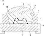
- FIG. 2 is a front sectional view showing an optical semiconductor device obtained by the method for manufacturing an optical semiconductor device according to the second embodiment of the present invention.
- the optical semiconductor device 11 shown in FIG. 2 includes a package 2 that is a constituent member of an optical semiconductor device formed of a resin material.
- An optical semiconductor element 3 is disposed in the frame 2 a of the package 2.
- the sealing agent 12 is filled in the frame portion 2 a so as to seal the optical semiconductor element 3. That is, the optical semiconductor element 3 is sealed with the sealant 12 in the frame 2 a of the package 2.
- the sealant 12 is in contact with the package 2 formed of a resin material on the inner surface of the frame portion 2a. Therefore, the sealing agent 12 is in contact with the package 2 formed of a resin material. It is preferable that the sealing agent 12 is formed by hardening the sealing agent which is a curable composition.
- a lens 13 is disposed on the sealant 12.
- the outer peripheral edge of the lower surface of the lens 13 is in contact with the upper surface of the frame portion 2a. Therefore, the lens 13 is in contact with the package 2 made of a resin material on the upper surface of the frame portion 2a.
- the lens 13 is preferably formed by curing a lens material that is a curable composition.
- FIG. 3 is a front sectional view showing an optical semiconductor device obtained by the method for manufacturing an optical semiconductor device according to the third embodiment of the present invention.
- an optical semiconductor element 23 is disposed on a substrate 22 on which a terminal 26 is disposed on the upper surface.
- the substrate 22 is an optical semiconductor device constituent member made of a resin material.
- An electrode 23 a disposed on the upper surface of the optical semiconductor element 23 and a terminal 26 disposed on the upper surface of the substrate 22 are electrically connected by a bonding wire 24.
- a lens 25 is disposed on the optical semiconductor element 23.
- the lens 25 covers the surface of the optical semiconductor element 23 and the bonding wire 24.
- the lens 25 is in contact with the substrate 22 made of a resin material.
- the lens 25 is preferably formed by curing a lens material that is a curable composition.
- the surface of the package 2 in contact with the sealants 4 and 12 and the lens 13 is subjected to plasma treatment.
- the surface of the package 2 is plasma-treated before the sealing agents 4 and 12 and the lens 13 are arranged, that is, before the sealing agents 4 and 12 and the lens 13 are in contact with each other.
- Sealants 4 and 12 and a lens 13 are arranged so as to come into contact with the package 2 after the plasma treatment.
- the sealing agents 4 and 12 and the lens 13 are disposed so as to be in contact with the frame portion 2a.
- the surface of the substrate 22 in contact with the lens 25 is subjected to plasma treatment.
- the surface of the substrate 22 is subjected to plasma treatment before the lens 25 is disposed, that is, before the lens 25 contacts.
- a lens is disposed so as to be in contact with the substrate 22 after the plasma processing.
- FIGS. 1 to 3 are merely examples of the optical semiconductor device according to the present invention, and the mounting structure of the optical semiconductor device can be modified as appropriate.
- the surface of the optical semiconductor device constituent member formed of a resin material that contacts the sealing agent is preferably subjected to plasma treatment, and the surface of the optical semiconductor device constituent member formed of a resin material that contacts the lens is plasma treated. It is also preferable to process. Moreover, it is preferable to plasma-process a frame part.
- the plasma treatment method includes a direct method in which a plasma discharge is generated between two electrodes to which a voltage is applied and a workpiece is passed between the electrodes, and an electrode in which the plasma discharge is generated.
- a remote method in which a plasma process is performed by blowing gas from between electrodes through a gas flow between the electrodes and spraying the plasma gas on an object to be processed. Of these, the remote method is preferable. It is preferable to plasma-treat the surface of the optical semiconductor device constituent member in contact with the sealing agent or the lens by spraying plasma gas onto the optical semiconductor device constituent member formed of a resin material by a remote method.
- a plasma generation method in the plasma treatment there are a first method using a gas in which a small amount of helium gas is mixed as a discharge gas, and a second method of applying a voltage as a pulse wave.
- a method for generating plasma there is also a third method for generating plasma in a reduced pressure atmosphere. Plasma generated by any one of the first, second, and third methods may be used. Plasma generated by a method different from the first, second, and third methods may be used.
- the third method In the third method, a chamber and a decompression pump for decompressing are required, and in addition to the processing apparatus becoming large and expensive, the inside of the chamber is decompressed after the object to be processed is placed in the chamber, After performing the plasma treatment, a complicated operation of releasing the reduced pressure and taking out the object to be processed is necessary. Therefore, the third method has a problem that it is inferior in productivity.
- the kinetic energy of gas molecules converted into plasma by depressurization becomes very high, and so-called “burn” discoloration may occur in the package resin that is the object to be processed.
- gases such as helium, argon, nitrogen, neon and oxygen are used. Moreover, you may use these mixed gas and air as discharge gas. From the viewpoint of reducing cost, it is preferable to use argon or nitrogen.
- oxygen is easily introduced into the surface of the optical semiconductor device constituent member during plasma processing, and efficiency In particular, it is possible to improve the adhesiveness.
- the oxygen concentration in the discharge gas is high, the processing efficiency is improved.
- the oxygen concentration in discharge gas is 30 volume% or less.
- the processing conditions for the plasma processing can be appropriately set depending on the structure and capability of the plasma processing apparatus to be used. Changes in surface energy due to plasma treatment can be evaluated by water contact angle. For example, a water contact angle on a clean surface of a polyphthalamide resin generally used as an optical semiconductor device constituent member is 75 to 80 degrees. After the plasma treatment, the water contact angle is preferably 60 degrees or less, more preferably 55 degrees or less, and still more preferably 45 degrees or less.
- the plasma treatment may be performed before the placement of the optical semiconductor element or after the placement of the optical semiconductor element.
- the plasma treatment may be performed after the connection between the electrode of the optical semiconductor element and the lead frame, or may be performed before the connection between the electrode of the optical semiconductor element and the lead frame.
- the optical semiconductor device constituent member is formed of a resin material and is a package or a substrate.
- the said optical semiconductor device structural member is arrange
- the optical semiconductor device constituent member is preferably a package, and is preferably a substrate.
- the optical semiconductor device constituent member and the package preferably have a frame portion.
- the sealant or the lens is preferably arranged in the frame part or on the frame part, and more preferably in the frame part. When the sealant or the lens is disposed in the frame portion, the sealant and the lens have a portion disposed in the frame portion and a portion disposed outside the frame portion. It may be.
- the optical semiconductor element is preferably arranged in the frame portion.
- the resin material that is a material of the optical semiconductor device constituent member includes a resin.
- the resin may be a thermoplastic resin or a thermosetting resin.
- the resin include polyphthalamide, polycyclohexylene terephthalate, epoxy resin, and silicone resin. Among them, polyphthalamide is widely used as the resin in the package for filling the sealant.
- the resin material may contain a filler in addition to the resin.
- a white filler is preferably used as the filler.
- examples of the white filler include titanium oxide and zinc oxide.
- the optical semiconductor device constituent member and the package can be obtained by arranging a lead frame serving as an electrode at a predetermined position and molding the resin material by transfer molding or the like.
- the lead frame is embedded in, for example, the optical semiconductor device constituent member and the package.
- Examples of the lead frame include a lead frame whose surface of a copper foil is silver-plated.
- the copper foil is generally processed into a predetermined shape by punching or etching.
- the optical semiconductor element is not particularly limited as long as it is a light emitting element using a semiconductor.
- the optical semiconductor element is a light emitting diode
- a structure in which an LED semiconductor material is stacked on a substrate can be mentioned.
- the semiconductor material include GaAs, GaP, GaAlAs, GaAsP, AlGaInP, GaN, InN, AlN, InGaAlN, and SiC.
- Examples of the material of the substrate include sapphire, spinel, SiC, Si, ZnO, and GaN single crystal. Further, a buffer layer may be formed between the substrate and the semiconductor material as necessary. Examples of the material of the buffer layer include GaN and AlN.
- optical semiconductor device examples include a light emitting diode device, a semiconductor laser device, and a photocoupler.
- Such optical semiconductor devices include, for example, backlights such as liquid crystal displays, illumination, various sensors, light sources such as printers and copiers, vehicle measuring instrument light sources, signal lights, indicator lights, display devices, and light sources for planar light emitters. It is suitably used for displays, decorations, various lights and switching elements.
- the shape of the lens is not particularly limited. From the viewpoint of controlling the light emission direction in the optical semiconductor device and further suppressing the front luminance from becoming too high, the shape of the lens may be a part of a sphere or a part of a spheroid. preferable.
- the sealant and the lens are preferably formed by curing a curable composition.
- the curable composition includes a first organopolysiloxane having two or more alkenyl groups, a second organopolysiloxane having two or more hydrogen atoms bonded to silicon atoms, and a hydrosilylation reaction catalyst. It is preferable. From the viewpoint of further suppressing the sealing agent and the lens (cured product) from peeling from the optical semiconductor device constituent member, the curable composition preferably contains an adhesion-imparting agent.
- the optical semiconductor device is used in a harsh environment under high temperature and high humidity. However, it becomes difficult for the sealant and the lens to be peeled off from the optical semiconductor device constituent member.
- the sealing agent or the lens when the sealing agent or the lens is formed using the curable composition, the sealing agent and the lens are difficult to peel from the light conductor device constituent member.
- the material of the package that contacts the sealant or the lens may be polyphthalamide (PPA).
- PPA polyphthalamide
- an electrode plated with silver may be formed on the back surface of the light emitting element. It is strongly required that the cured product has high adhesion to a package or electrode formed of such PPA. When the cured product is peeled off from the package or the electrode or the adhesion is low, the amount of light (luminous intensity) emitted from the optical semiconductor device decreases.
- the present inventor has adopted the above-described first and second compositions by employing a composition containing the first and second organopolysiloxanes and the hydrosilylation reaction catalyst and the first silane compound having a ureido group. Compared to the composition containing the first silane compound having a ureido group together with an organopolysiloxane and a hydrosilylation reaction catalyst, adhesion to an optical semiconductor device component formed by a resin material for a sealant and a lens It was found that can be sufficiently increased.
- the first organopolysiloxane is represented by the formula (1A) and is a first organopolysiloxane having an alkenyl group and a methyl group bonded to a silicon atom, or represented by the formula (1B) and an aryl A first organopolysiloxane having a group and an alkenyl group is preferred.
- the first organopolysiloxane represented by the formula (1A) and the formula (1B) has two or more alkenyl groups.
- a first organopolysiloxane different from the first organopolysiloxane represented by the formula (1A) or the formula (1B) may be used.
- the first organopolysiloxane preferably does not have a hydrogen atom bonded to a silicon atom.
- the first organopolysiloxane preferably does not have a hydrogen atom bonded to a silicon atom.
- the second organopolysiloxane is a second organopolysiloxane represented by the formula (51A) and having a hydrogen atom bonded to a silicon atom and a methyl group bonded to a silicon atom, or the formula (51B) And is preferably a second organopolysiloxane having an aryl group and a hydrogen atom bonded to a silicon atom.
- the second organopolysiloxane represented by the formula (51A) and the formula (51B) has two or more hydrogen atoms bonded to silicon atoms.
- a second organopolysiloxane different from the second organopolysiloxane represented by the formula (51A) or the formula (51B) may be used.
- the first organopolysiloxane is represented by the formula A first organopolysiloxane represented by (1A) having an alkenyl group and a methyl group bonded to a silicon atom
- the second organopolysiloxane is represented by the formula (51A) and bonded to a silicon atom
- the first organopolysiloxane represented by the formula (1B) having an aryl group and an alkenyl group.
- the second organopolysiloxane is represented by the formula (51B) and bonded to an aryl group and a silicon atom.
- A is preferably a second organopolysiloxane having a hydrogen
- a cured product of a conventional curable composition when used in a harsh environment such as a temperature cycle that repeatedly receives heating and cooling, the cured product may crack, or the cured product may be peeled off from a package or the like. There are things to do.
- a cured product of a conventional curable composition has a problem that heat resistance is low.
- the first organopolysiloxane is a first organopolysiloxane represented by the formula (1A) and having an alkenyl group and a methyl group bonded to a silicon atom.
- the second organopolysiloxane is preferably the second organopolysiloxane represented by the formula (51A) and having a hydrogen atom bonded to a silicon atom and a methyl group bonded to a silicon atom.
- the number ratio of methyl groups is 80% or more among all functional groups bonded to silicon atoms of the first organopolysiloxane. From the viewpoint of obtaining a cured product that is more excellent in heat resistance, it is preferable that the number ratio of methyl groups is 80% or more among all functional groups bonded to silicon atoms of the second organopolysiloxane.
- the number ratio of methyl groups is more preferably 85% or more, still more preferably 90% or more, and preferably 99.9. % Or less, more preferably 99% or less, and still more preferably 98% or less.
- the number ratio of methyl groups is 80% or more, the heat resistance of the cured product is increased, and even if the optical semiconductor device is used in a harsh environment under high temperature and high humidity, the cured product can be used. Is less likely to occur and the luminous intensity is less reduced. Moreover, the heat resistance of hardened
- alkenyl groups can be sufficiently introduced into the first organopolysiloxane, and hydrogen atoms bonded to silicon atoms can be sufficiently introduced into the second organopolysiloxane, It is easy to improve the curability of the curable composition.
- a silver-plated electrode may be formed on the back surface of the light emitting element in order to reflect the light reaching the back side of the light emitting element. If a crack occurs in the sealant or the lens, or the sealant is peeled off from the optical semiconductor device constituent member, the silver-plated electrode is exposed to the atmosphere or easily touched with the atmosphere. As a result, the silver plating may be discolored by a corrosive gas such as hydrogen sulfide gas or sulfurous acid gas present in the atmosphere. When the color of the electrode changes, the reflectance decreases, which causes a problem that the brightness of the light emitted from the light emitting element decreases.
- a corrosive gas such as hydrogen sulfide gas or sulfurous acid gas
- the encapsulant or lens which is a cured product of the curable composition, has a high gas barrier property against corrosive gas, thereby suppressing discoloration of silver plating and suppressing a decrease in brightness of light emitted from the light emitting element. it can.
- the first organopolysiloxane is the first organopolysiloxane represented by the formula (1B) and having an aryl group and an alkenyl group
- the first The second organopolysiloxane represented by the formula (51B) is preferably a second organopolysiloxane having an aryl group and a hydrogen atom bonded to a silicon atom.
- the number ratio of the aryl group is 30% or more and 70% or less. Is preferred. From the viewpoint of obtaining a cured product that is more excellent in gas barrier properties, the ratio of the number of aryl groups in the total functional groups bonded to silicon atoms of the second organopolysiloxane is 30% or more and 70% or less. Is preferred.
- the number ratio of the aryl group is more preferably 35% or more, and more preferably 65% or less.
- the number ratio of the aryl group is equal to or more than the above lower limit, the gas barrier property of the cured product is further enhanced, and cracks and peeling are less likely to occur in the cured product.
- peeling of the cured product is more difficult to occur.
- the number ratio of the aryl group indicates the number ratio of the phenyl group.
- the curing temperature of the curable composition is not particularly limited.
- the curing temperature of the curable composition is preferably 80 ° C. or higher, more preferably 100 ° C. or higher, preferably 180 ° C. or lower, more preferably 160 ° C. or lower.
- the curing temperature is equal to or higher than the lower limit, the curing of the curable composition proceeds sufficiently.
- the curing temperature is not more than the above upper limit, the package is unlikely to be thermally deteriorated.
- the first organopolysiloxane contained in the curable composition has two or more alkenyl groups.
- the alkenyl group is preferably directly bonded to the silicon atom.
- the carbon atom in the carbon-carbon double bond of the alkenyl group may be bonded to the silicon atom, and the carbon atom different from the carbon atom in the carbon-carbon double bond of the alkenyl group is bonded to the silicon atom. It may be bonded.
- As for said 1st organopolysiloxane only 1 type may be used and 2 or more types may be used together.
- the first organopolysiloxane is represented by the following formula (1A), and includes a first organopolysiloxane having an alkenyl group and a methyl group bonded to a silicon atom.
- Siloxane hereinafter sometimes referred to as first organopolysiloxane A
- the first organopolysiloxane A is preferably a first organopolysiloxane which does not have a hydrogen atom bonded to a silicon atom but has an alkenyl group and a methyl group bonded to a silicon atom.
- R1 to R6 each represents at least one alkenyl group, at least one represents a methyl group, and R1 to R6 other than the alkenyl group and the methyl group represent a hydrocarbon group having 2 to 8 carbon atoms. .
- the first organopolysiloxane is represented by the following formula (1B), and includes a first organopolysiloxane having an aryl group and an alkenyl group (hereinafter referred to as the first organopolysiloxane). 1 may be referred to as organopolysiloxane B).
- the first organopolysiloxane B is preferably a first organopolysiloxane which does not have a hydrogen atom bonded to a silicon atom and has an aryl group and an alkenyl group.
- the aryl group include an unsubstituted phenyl group and a substituted phenyl group.
- the structural unit represented by (R4R5SiO 2/2 ) and the structural unit represented by (R6SiO 3/2 ) each have an alkoxy group. It may have a hydroxy group.
- the above formula (1A) and the above formula (1B) show an average composition formula.
- the hydrocarbon group in the above formula (1A) and the above formula (1B) may be linear or branched.
- R1 to R6 in the above formula (1A) and the above formula (1B) may be the same or different.
- the oxygen atom part in the structural unit represented by (R4R5SiO 2/2 ) and the oxygen atom part in the structural unit represented by (R6SiO 3/2 ) are respectively siloxane.
- An oxygen atom part forming a bond, an oxygen atom part of an alkoxy group, or an oxygen atom part of a hydroxy group is shown.
- the content of alkoxy groups is small, and the content of hydroxy groups is also small.
- an organosilicon compound such as an alkoxysilane compound is hydrolyzed and polycondensed to obtain a first organopolysiloxane
- most of the alkoxy groups and hydroxy groups are converted into a partial skeleton of siloxane bonds. It is to be done. That is, most of oxygen atoms of the alkoxy group and oxygen atoms of the hydroxy group are converted into oxygen atoms forming a siloxane bond.
- alkenyl group examples include vinyl group, allyl group, butenyl group, pentenyl group, and hexenyl group.
- the alkenyl group in the first organopolysiloxane and the alkenyl group in the above formula (1A) and the above formula (1B) are preferably vinyl groups or allyl groups. More preferably, it is a group.
- the first organopolysiloxane preferably has a vinyl group.
- the hydrocarbon group having 2 to 8 carbon atoms in the above formula (1A) is not particularly limited, and examples thereof include ethyl group, n-propyl group, n-butyl group, n-pentyl group, n-hexyl group, and n-heptyl. Group, n-octyl group, isopropyl group, isobutyl group, sec-butyl group, t-butyl group, isopentyl group, neopentyl group, t-pentyl group, isohexyl group, cyclohexyl group and aryl group.
- Examples of the hydrocarbon group having 1 to 8 carbon atoms in the above formula (1B) include the same groups as the hydrocarbon group having 2 to 8 carbon atoms in the above formula (1A), and further includes a methyl group.
- the first organopolysiloxane A preferably has an aryl group.
- the aryl group include an unsubstituted phenyl group and a substituted phenyl group.
- the number ratio of the aryl group is preferably 0.5% or more, preferably 10% or less, more preferably 5% or less.
- the structural unit represented by (R4R5SiO 2/2 ) (hereinafter also referred to as a bifunctional structural unit) has the following formula ( The structure represented by 1-2), that is, a structure in which one of the oxygen atoms bonded to the silicon atom in the bifunctional structural unit forms a hydroxy group or an alkoxy group may be included.
- the structural unit represented by (R4R5SiO 2/2 ) includes a portion surrounded by a broken line of the structural unit represented by the following formula (1-b), and is further represented by the following formula (1-2-b). A portion surrounded by a broken line of the structural unit may be included. That is, a structural unit having a group represented by R4 and R5 and having an alkoxy group or a hydroxy group remaining at the terminal is also included in the structural unit represented by (R4R5SiO 2/2 ).
- the structural unit represented by (R4R5SiO 2/2 ) is a broken line of the structural unit represented by the following formula (1-b) The part enclosed by is shown.
- the structural unit represented by (R4R5SiO 2/2 ) having the remaining alkoxy group or hydroxy group has the following formula: A portion surrounded by a broken line in the structural unit represented by (1-2-b) is shown.
- the oxygen atom in the Si—O—Si bond forms a siloxane bond with the adjacent silicon atom, and the adjacent structural unit and oxygen atom Sharing. Accordingly, one oxygen atom in the Si—O—Si bond is defined as “O 1/2 ”.
- X represents OH or OR
- OR represents a linear or branched alkoxy group having 1 to 4 carbon atoms.
- R4 and R5 in formula (1-b), formula (1-2), and formula (1-2-b) are the same groups as R4 and R5 in formula (1A) and formula (1B). It is.
- the structural unit represented by (R6SiO 3/2 ) (hereinafter also referred to as trifunctional structural unit) has the following formula ( 1-3) or a structure represented by formula (1-4), that is, a structure in which two oxygen atoms bonded to a silicon atom in a trifunctional structural unit each constitute a hydroxy group or an alkoxy group, or a trifunctional
- One of the oxygen atoms bonded to the silicon atom in the structural unit may include a structure constituting a hydroxy group or an alkoxy group.
- the structural unit represented by (R6SiO 3/2 ) includes a portion surrounded by a broken line of the structural unit represented by the following formula (1-c), and further includes the following formula (1-3-c) or formula ( A portion surrounded by a broken line of the structural unit represented by 1-4-4-c) may be included. That is, a structural unit having a group represented by R6 and having an alkoxy group or a hydroxy group remaining at the terminal is also included in the structural unit represented by (R6SiO 3/2 ).
- R6 in the above formula (1-c), formula (1-3), formula (1-3-c), formula (1-4) and formula (1-4-c) represents the above formula (1A) and It is the same group as R6 in the above formula (1B).
- the linear or branched alkoxy group having 1 to 4 carbon atoms is not particularly limited.
- the lower limit of a / (a + b + c) is 0, and the upper limit is 0.30.
- a / (a + b + c) is less than or equal to the above upper limit, the heat resistance of the cured product is further increased, and peeling of the cured product can be further suppressed.
- a / (a + b + c) becomes like this. Preferably it is 0.25 or less, More preferably, it is 0.20 or less.
- the lower limit of b / (a + b + c) is 0.70, and the upper limit is 1.0.
- b / (a + b + c) is not less than the above lower limit, the cured product does not become too hard, and cracks hardly occur in the cured product.
- b / (a + b + c) is preferably 0.75 or more, more preferably 0.80 or more.
- the lower limit of c / (a + b + c) is 0, and the upper limit is 0.10.
- c / (a + b + c) is not more than the above upper limit, it is easy to maintain an appropriate viscosity of the curable composition, and the adhesiveness of the cured product is further enhanced.
- c / (a + b + c) is preferably 0.05 or less.
- the structural unit of (R6SiO 3/2 ) does not exist in the above formula (1A).
- the first organopolysiloxane represented by the above formula (1A) is preferably the first organopolysiloxane represented by the following formula (1Aa).
- a / (a + b) is preferably 0.25 or less, more preferably 0.20 or less, and still more preferably 0.15 or less.
- b / (a + b) is preferably 0.75 or more, more preferably 0.80 or more, and further preferably 0.85 or more.
- a / (a + b + c) is 0 or more and 0.50 or less.
- a / (a + b + c) is less than or equal to the above upper limit, the heat resistance of the cured product is further increased, and peeling of the cured product can be further suppressed.
- a / (a + b + c) is preferably 0.45 or less, more preferably 0.40 or less.
- b / (a + b + c) is 0.40 or more and 1.0 or less.
- b / (a + b + c) is not less than the above lower limit, the cured product does not become too hard, and cracks hardly occur in the cured product.
- b / (a + b + c) is preferably 0.50 or more.
- c / (a + b + c) is 0 or more and 0.50 or less.
- c / (a + b + c) is not more than the above upper limit, it is easy to maintain an appropriate viscosity of the curable composition, and the adhesiveness of the cured product is further enhanced.
- c / (a + b + c) is preferably 0.45 or less, more preferably 0.40 or less, and still more preferably 0.35 or less.
- the structural unit of (R6SiO 3/2 ) does not exist in the above formula (1B).
- C / (a + b + c) in the above formula (1B) is preferably 0. That is, the first organopolysiloxane represented by the above formula (1B) is preferably the first organopolysiloxane represented by the following formula (1Bb). As a result, cracks are less likely to occur in the cured product, and peeling of the cured product is further less likely to occur.
- a / (a + b) in the above formula (1Bb) is preferably 0.45 or less, more preferably 0.40 or less.
- b / (a + b) is preferably 0.55 or more, more preferably 0.60 or more.
- NMR si-nuclear magnetic resonance analysis
- TMS tetramethylsilane
- Each peak corresponding to the structural unit represented by (R4R5SiO 2/2 ) and the bifunctional structural unit of the above formula (1-2) appears in the vicinity of ⁇ 10 to ⁇ 50 ppm, and the above formula (1A) and the above formula (1B )
- the peaks corresponding to the structural unit represented by (R6SiO 3/2 ) and the trifunctional structural units of the above formulas (1-3) and (1-4) are in the vicinity of ⁇ 50 to ⁇
- the ratio of each structural unit in the above formula (1A) and the above formula (1B) can be measured by measuring 29 Si-NMR and comparing the peak areas of the respective signals.
- the second organopolysiloxane contained in the curable composition has two or more hydrogen atoms bonded to silicon atoms.
- the hydrogen atom is directly bonded to the silicon atom.
- As for said 2nd organopolysiloxane only 1 type may be used and 2 or more types may be used together.
- the second organopolysiloxane is represented by the following formula (51A) and has a hydrogen atom bonded to a silicon atom and a methyl group bonded to the silicon atom.
- a second organopolysiloxane (hereinafter sometimes referred to as a second organopolysiloxane A) is preferred.
- R51 to R56 each represents at least one hydrogen atom, at least one represents a methyl group, and R51 to R56 other than the hydrogen atom and the methyl group are hydrocarbon groups having 2 to 8 carbon atoms. Represents.
- the second organopolysiloxane is represented by the following formula (51B), and includes a second organopolysiloxane having an aryl group and a hydrogen atom bonded to a silicon atom.
- Siloxane hereinafter sometimes referred to as second organopolysiloxane B
- the aryl group include an unsubstituted phenyl group and a substituted phenyl group.
- R51 to R56 represents an aryl group
- R51 to R56 other than the aryl group and the hydrogen atom are carbon atoms having 1 to 8 carbon atoms. Represents a hydrogen group.
- the structural unit represented by (R54R55SiO 2/2 ) and the structural unit represented by (R56SiO 3/2 ) each have an alkoxy group. It may have a hydroxy group.
- the above formula (51A) and the above formula (51B) show the average composition formula.
- the hydrocarbon group in the above formula (51A) and the above formula (51B) may be linear or branched.
- R51 to R56 in the above formula (51A) and the above formula (51B) may be the same or different.
- the oxygen atom part in the structural unit represented by (R54R55SiO 2/2 ) and the oxygen atom part in the structural unit represented by (R56SiO 3/2 ) are respectively siloxane.
- An oxygen atom part forming a bond, an oxygen atom part of an alkoxy group, or an oxygen atom part of a hydroxy group is shown.
- the hydrocarbon group having 2 to 8 carbon atoms in the above formula (51A) is not particularly limited, and examples thereof include the same hydrocarbon groups as those having 2 to 8 carbon atoms in the above formula (1A).
- Examples of the hydrocarbon group having 1 to 8 carbon atoms in the above formula (51B) include the same groups as the hydrocarbon group having 2 to 8 carbon atoms in the above formula (1A), and further includes a methyl group.
- the second organopolysiloxane preferably has an alkenyl group, and more preferably has a vinyl group.
- at least one of R51 to R56 represents a silicon atom, at least one represents a methyl group, at least one represents an alkenyl group, a hydrogen atom, a methyl group, and R51 to R56 other than the alkenyl group represent a hydrocarbon group having 2 to 8 carbon atoms.
- At least one of R51 to R56 represents an aryl group, at least one represents a silicon atom, at least one represents an alkenyl group, and other than an aryl group, a hydrogen atom, and an alkenyl group R51 to R56 each represents a hydrocarbon group having 2 to 8 carbon atoms.
- the second organopolysiloxane A preferably has an aryl group.
- the aryl group include an unsubstituted phenyl group and a substituted phenyl group.
- the number ratio of the aryl group is preferably 0.5% or more, preferably 10% or less, more preferably 5% or less.
- the structural unit represented by (R54R55SiO 2/2 ) (hereinafter also referred to as a bifunctional structural unit) has the following formula ( 51-2), that is, a structure in which one of oxygen atoms bonded to a silicon atom in the bifunctional structural unit constitutes a hydroxy group or an alkoxy group may be included.
- the structural unit represented by (R54R55SiO 2/2 ) includes a portion surrounded by a broken line of the structural unit represented by the following formula (51-b), and is further represented by the following formula (51-2-b). A portion surrounded by a broken line of the structural unit may be included. That is, a structural unit having a group represented by R54 and R55 and having an alkoxy group or a hydroxy group remaining at the terminal is also included in the structural unit represented by (R54R55SiO 2/2 ).
- X represents OH or OR
- OR represents a linear or branched alkoxy group having 1 to 4 carbon atoms.
- R54 and R55 in the formula (51-b), formula (51-2) and formula (51-2-b) are the same groups as R54 and R55 in the formula (51A) and the formula (51B). It is.
- the structural unit represented by (R56SiO 3/2 ) (hereinafter also referred to as trifunctional structural unit) has the following formula ( 51-3) or a structure represented by formula (51-4), that is, a structure in which two oxygen atoms bonded to a silicon atom in a trifunctional structural unit each constitute a hydroxy group or an alkoxy group, or a trifunctional
- One of the oxygen atoms bonded to the silicon atom in the structural unit may include a structure constituting a hydroxy group or an alkoxy group.
- the structural unit represented by (R56SiO 3/2 ) includes a portion surrounded by a broken line of the structural unit represented by the following formula (51-c), and further includes the following formula (51-3-c) or formula ( A part surrounded by a broken line of the structural unit represented by 51-4-c) may be included. That is, a structural unit having a group represented by R56 and having an alkoxy group or a hydroxy group remaining at the terminal is also included in the structural unit represented by (R56SiO 3/2 ).
- R56 in the above formula (51-c), formula (51-3), formula (51-3-c), formula (51-4) and formula (51-4-c) represents the above formula (51A) and It is the same group as R56 in the above formula (51B).
- the linear or branched alkoxy group having 1 to 4 carbon atoms is not particularly limited.
- the lower limit of p / (p + q + r) is 0.10 and the upper limit is 0.50.
- p / (p + q + r) is less than or equal to the above upper limit, the hardness of the cured product is increased, adhesion of scratches and dust can be prevented, the heat resistance of the cured product is further increased, and peeling of the cured product can be further suppressed.
- p / (p + q + r) becomes like this. Preferably it is 0.45 or less, More preferably, it is 0.40 or less.
- the lower limit of q / (p + q + r) is 0, and the upper limit is 0.40.
- q / (p + q + r) exceeds 0, the cured product does not become too hard and cracks are hardly generated in the cured product.
- q / (p + q + r) becomes like this.
- it is 0.10 or more, More preferably, it is 0.15 or more.
- the structural unit of (R54R55SiO 2/2 ) does not exist in the above formula (51A).
- the lower limit of r / (p + q + r) is 0.40, and the upper limit is 0.90.
- r / (p + q + r) is not less than the above lower limit, the hardness of the cured product is increased, and scratches and dust can be prevented from adhering.
- r / (p + q + r) is not more than the above upper limit, it is easy to maintain an appropriate viscosity of the curable composition, and the adhesiveness of the cured product is further enhanced.
- p / (p + q + r) is 0.05 or more and 0.50 or less.
- p / (p + q + r) is less than or equal to the above upper limit, the heat resistance of the cured product is further increased, and peeling of the cured product can be further suppressed.
- p / (p + q + r) becomes like this.
- it is 0.10 or more, Preferably it is 0.45 or less.
- q / (p + q + r) is 0.05 or more and 0.50 or less.
- q / (p + q + r) is not less than the above lower limit, the cured product does not become too hard and cracks are hardly generated in the cured product.
- q / (p + q + r) is not more than the above upper limit, the gas barrier property of the cured product is further enhanced.
- q / (p + q + r) becomes like this. Preferably it is 0.10 or more, More preferably, it is 0.45 or less.
- r / (p + q + r) is 0.20 or more and 0.80 or less.
- r / (p + q + r) is equal to or greater than the above lower limit, the hardness of the cured product is increased, scratches and dust can be prevented, the heat resistance of the cured product is increased, and the thickness of the cured product is less likely to decrease in a high temperature environment.
- r / (p + q + r) is not more than the above upper limit, it is easy to maintain an appropriate viscosity of the curable composition, and the adhesiveness of the cured product is further enhanced.
- the ratio of each structural unit in the above formula (51A) and the above formula (51B) can be measured by measuring 29 Si-NMR and comparing the peak areas of the respective signals.
- the content of the second organopolysiloxane is preferably 10 parts by weight or more, more preferably 15 parts by weight or more, still more preferably 20 parts by weight or more, preferably 100 parts by weight of the first organopolysiloxane. 400 parts by weight or less, more preferably 300 parts by weight or less, still more preferably 200 parts by weight or less.
- a curable composition more excellent in curability can be obtained.
- the number average molecular weight (Mn) of the first organopolysiloxane is preferably 500 or more, more preferably 1000 or more, still more preferably 5000 or more, preferably 200000 or less, more preferably 100000 or less, still more preferably 60000 or less, Particularly preferred is 10,000 or less, and most preferred is 8000 or less.
- the number average molecular weight (Mn) of the first organopolysiloxane represented by the above formula (1A) is preferably 500 or more, more preferably 1000 or more, further preferably 5000 or more, preferably 200000 or less, more preferably 100000. Hereinafter, it is more preferably 60000 or less.
- the number average molecular weight (Mn) of the first organopolysiloxane represented by the above formula (1B) is preferably 500 or more, more preferably 1000 or more, preferably 10,000 or less, more preferably 8000 or less.
- the number average molecular weight (Mn) of the second organopolysiloxane is preferably 500 or more, more preferably 1000 or more, preferably 20000 or less, more preferably 10,000 or less.
- the number average molecular weight (Mn) is a value obtained by using polystyrene as a standard substance using gel permeation chromatography (GPC).
- the number average molecular weight (Mn) is determined by two measuring devices manufactured by Waters (column: Shodex GPC LF-804 (length: 300 mm) manufactured by Showa Denko KK), measuring temperature: 40 ° C., flow rate: 1 mL / min, solvent: Tetrahydrofuran, standard substance: polystyrene) means a value measured.
- the method for synthesizing the first and second organopolysiloxanes is not particularly limited, and examples thereof include a method in which an alkoxysilane compound is hydrolyzed and subjected to a condensation reaction, and a method in which a chlorosilane compound is hydrolyzed and condensed. Especially, the method of hydrolyzing and condensing an alkoxysilane compound from a viewpoint of reaction control is preferable.
- Examples of the method of hydrolyzing and condensing the alkoxysilane compound include a method of reacting an alkoxysilane compound in the presence of water and an acidic catalyst or a basic catalyst. Further, the disiloxane compound may be hydrolyzed and used.
- organosilicon compound for introducing an alkenyl group into the first organopolysiloxane examples include vinyltrimethoxysilane, vinyltriethoxysilane, vinylmethyldimethoxysilane, methoxydimethylvinylsilane, vinyldimethylethoxysilane, and 1,3-divinyl. -1,1,3,3-tetramethyldisiloxane and the like.
- organosilicon compound for introducing a hydrogen atom bonded to a silicon atom into the second organopolysiloxane examples include trimethoxysilane, triethoxysilane, methyldimethoxysilane, methyldiethoxysilane, and 1,1,3, Examples include 3-tetramethyldisiloxane.
- organosilicon compound for introducing an aryl group into the first and second organopolysiloxanes as necessary include triphenylmethoxysilane, triphenylethoxysilane, diphenyldimethoxysilane, diphenyldiethoxysilane, methyl (phenyl) ) Dimethoxysilane, phenyltrimethoxysilane and the like.
- organosilicon compounds examples include silane, cyclohexyl (methyl) dimethoxysilane, methyltrimethoxysilane, methyltriethoxysilane, ethyltrimethoxysilane, ethyltriethoxysilane, hexyltrimethoxysilane, and octyltrimethoxysilane.
- Examples of the acidic catalyst include inorganic acids, organic acids, acid anhydrides of inorganic acids and derivatives thereof, and acid anhydrides of organic acids and derivatives thereof.
- the hydrosilylation reaction catalyst contained in the curable composition comprises hydrosilylation of an alkenyl group in the first organopolysiloxane and a hydrogen atom bonded to a silicon atom in the second organopolysiloxane. The catalyst to be reacted.
- hydrosilylation reaction catalyst various catalysts that cause the hydrosilylation reaction to proceed can be used.
- the said catalyst for hydrosilylation reaction only 1 type may be used and 2 or more types may be used together.
- hydrosilylation reaction catalyst examples include platinum-based catalysts, rhodium-based catalysts, and palladium-based catalysts. Since the transparency of the cured product is increased, a platinum-based catalyst is preferable.
- platinum-based catalyst examples include platinum powder, chloroplatinic acid, platinum-alkenylsiloxane complex, platinum-olefin complex, and platinum-carbonyl complex.
- platinum-alkenylsiloxane complex or a platinum-olefin complex is preferred.
- Examples of the alkenylsiloxane in the platinum-alkenylsiloxane complex include 1,3-divinyl-1,1,3,3-tetramethyldisiloxane and 1,3,5,7-tetramethyl-1,3,5. , 7-tetravinylcyclotetrasiloxane and the like.
- Examples of the olefin in the platinum-olefin complex include allyl ether and 1,6-heptadiene.
- alkenylsiloxane is preferably 1,3-divinyl-1,1,3,3-tetramethyldisiloxane.
- the organosiloxane oligomer is preferably a dimethylsiloxane oligomer.
- the olefin is preferably 1,6-heptadiene.
- the content of the catalyst for hydrosilylation reaction is preferably 0.01 ppm or more, more preferably 1 ppm or more, preferably in terms of weight units of metal atoms (platinum atoms in the case of platinum alkenyl complexes). Is 1000 ppm or less, more preferably 500 ppm or less.
- the content of the hydrosilylation reaction catalyst is not less than the above lower limit, it is easy to sufficiently cure the curable composition.
- the content of the catalyst for hydrosilylation reaction is not more than the above upper limit, the problem of coloring of the cured product hardly occurs.
- the curable composition preferably contains an adhesion-imparting agent.
- the adhesion imparting agent is preferably a silane coupling agent.
- the curable composition and the adhesion-imparting agent preferably include a first silane compound having a ureido group. .
- the first silane compound is preferably a first silane compound represented by the following formula (S1).
- X1 represents an alkoxy group
- X2 and X3 each represents an alkyl group or alkoxy group having 1 to 8 carbon atoms
- R4 is a single bond directly bonding a nitrogen atom and a silicon atom. Or a hydrocarbon group having 1 to 8 carbon atoms.
- the content of the adhesion-imparting agent is preferably 0.01 parts by weight or more, more preferably 0.1 parts by weight or more, preferably 10 parts by weight with respect to a total of 100 parts by weight of the first and second organopolysiloxanes. Part or less, more preferably 5 parts by weight or less, still more preferably 3 parts by weight or less.
- the content of the adhesion-imparting agent is equal to or more than the lower limit, peeling of the cured product from the object to be bonded can be further suppressed.
- the content of the adhesion-imparting agent is not more than the above upper limit, the excessive adhesion-imparting agent is less likely to volatilize, and the thickness of the cured product is less likely to decrease in a high-temperature environment.
- the content of the first silane compound is preferably 0.01 parts by weight or more, more preferably 0.1 parts by weight or more, preferably 100 parts by weight in total for the first and second organopolysiloxanes. 5 parts by weight or less, more preferably 3 parts by weight or less.
- the content of the first silane compound is equal to or higher than the lower limit, peeling of the cured product from the adhesion target can be further suppressed.
- the content of the first silane compound is less than or equal to the above upper limit, the excessive adhesion-imparting agent is less likely to volatilize, and the thickness of the cured product is less likely to decrease under a high temperature environment.
- the adhesion imparting agent preferably contains a second silane compound different from the first silane compound having a ureido group.
- a second silane compound different from the first silane compound having a ureido group.
- the second silane compound is not particularly limited, and examples thereof include vinyltriethoxysilane, vinyltrimethoxysilane, 3-glycidoxypropyltrimethoxysilane, 2- (3,4-epoxycyclohexyl) ethyltrimethoxysilane, Examples include 3- (meth) acryloxypropyltrimethoxysilane, ⁇ -aminopropyltrimethoxysilane, and N-phenyl-3-aminopropyltrimethoxysilane.
- (meth) acryloyl indicates acryloyl and methacryloyl.
- (meth) acryloxy refers to acryloxy and methacryloxy.
- the second silane compound preferably has an epoxy group, a vinyl group or a (meth) acryloyl group.
- the second silane compound is 3-glycidoxypropyltrimethoxysilane, 2- (3,4-epoxycyclohexyl) ethyltrimethoxysilane. Vinyltrimethoxysilane or 3- (meth) acryloxypropyltrimethoxysilane is preferable.
- the content of the second silane compound is preferably 0.01 parts by weight or more, more preferably 0.1 parts by weight or more, preferably 100 parts by weight based on the total of the first and second organopolysiloxanes. 5 parts by weight or less, more preferably 3 parts by weight or less.
- the content of the second silane compound is equal to or more than the lower limit, peeling of the cured product from the adhesion target can be further suppressed. If the content of the second silane compound is less than or equal to the above upper limit, the excess second silane coupling agent is less likely to volatilize, and the thickness of the cured product is less likely to decrease in a high temperature environment.
- the curable composition preferably further includes silicon oxide particles.
- the encapsulant preferably further contains silicon oxide particles.
- the primary particle diameter of the silicon oxide particles is preferably 5 nm or more, more preferably 8 nm or more, preferably 200 nm or less, more preferably 150 nm or less.
- the primary particle diameter of the silicon oxide particles is not less than the above lower limit, the dispersibility of the silicon oxide particles is further increased, and the transparency of the cured product is further increased.
- the primary particle diameter of the silicon oxide particles is not more than the above upper limit, the effect of increasing the viscosity at 25 ° C. can be sufficiently obtained, and the decrease in the viscosity due to the temperature increase can be suppressed.
- the BET specific surface area of the silicon oxide particles is preferably 30 m 2 / g or more, and preferably 400 m 2 / g or less.
- the BET specific surface area of the silicon oxide particles is 30 m 2 / g or more, the viscosity at 25 ° C. of the curable composition can be controlled within a suitable range, and the decrease in the viscosity due to a temperature rise can be suppressed.
- the BET specific surface area of the silicon oxide particles is 400 m 2 / g or less, the aggregation of the silicon oxide particles hardly occurs, the dispersibility can be increased, and the transparency of the cured product can be further increased. it can.
- the silicon oxide particles are not particularly limited, and examples thereof include silica produced by a dry method such as fumed silica and fused silica, and silica produced by a wet method such as colloidal silica, sol-gel silica and precipitated silica. It is done.
- fumed silica is suitably used as the silicon oxide particles from the viewpoint of obtaining a cured product with less volatile components and higher transparency.
- the silicon oxide particles are preferably surface-treated with an organosilicon compound. By this surface treatment, the dispersibility of the silicon oxide particles becomes very high, and it is possible to further suppress the decrease in the viscosity due to the temperature increase of the curable composition.
- the content of the silicon oxide particles is preferably 0.1 parts by weight or more, more preferably 0.5 parts by weight or more, still more preferably 1 with respect to 100 parts by weight of the total of the first and second organopolysiloxanes. Part by weight or more, preferably 40 parts by weight or less, more preferably 35 parts by weight or less, still more preferably 20 parts by weight or less.
- the content of the silicon oxide particles is equal to or higher than the lower limit, it is possible to suppress a decrease in viscosity at the time of curing.
- the content of the silicon oxide particles is not more than the above upper limit, the viscosity of the curable composition can be controlled to a more appropriate range, and the transparency of the cured product is further enhanced.
- the curable composition may further contain a phosphor.
- the sealant preferably further contains a phosphor.
- the said curable composition does not need to contain the fluorescent substance.
- a phosphor may be added when using the curable composition.
- the phosphor acts, for example, to absorb light emitted from a light-emitting element that is sealed using the curable composition and generate fluorescence, thereby finally obtaining light of a desired color. To do.
- the phosphor is excited by light emitted from the light emitting element to emit fluorescence, and light of a desired color is obtained by a combination of light emitted from the light emitting element and fluorescence emitted from the phosphor.
- the content of the phosphor can be adjusted as appropriate so as to obtain light of a desired color, and is not particularly limited.
- the content of the phosphor is preferably 0.1 parts by weight or more and preferably 40 parts by weight or less with respect to 100 parts by weight of the curable composition.
- the content of the phosphor is preferably 0.1 parts by weight or more and preferably 40 parts by weight or less with respect to 100 parts by weight of all components excluding the phosphor of the curable composition.
- the curable composition further contains an additive such as a dispersant, an antioxidant, an antifoaming agent, a colorant, a modifier, a leveling agent, a light diffusing agent, a heat conductive filler, or a flame retardant as necessary. You may go out.
- an additive such as a dispersant, an antioxidant, an antifoaming agent, a colorant, a modifier, a leveling agent, a light diffusing agent, a heat conductive filler, or a flame retardant as necessary. You may go out.
- Example 1 Synthesis of the first organopolysiloxane: 486 g of dimethyldimethoxysilane and 2.7 g of 1,3-divinyl-1,1,3,3-tetramethyldisiloxane were placed in a 1 L separable flask equipped with a thermometer, a dropping device, and a stirrer at 50 ° C. Stir. A solution prepared by dissolving 2.2 g of potassium hydroxide in 144 g of water was slowly added dropwise thereto, and after the addition, the mixture was stirred at 50 ° C. for 6 hours and reacted to obtain a reaction solution. Next, volatile components were removed under reduced pressure, 2.4 g of acetic acid was added to the reaction solution, and the mixture was heated under reduced pressure. Thereafter, potassium acetate was removed by filtration to obtain a polymer (A).
- the number average molecular weight of the obtained polymer (A) was 37400.
- the polymer (A) had the following average composition formula (A1).
- the molecular weight of the polymer was measured by GPC measurement by adding 1 mL of tetrahydrofuran to 10 mg, stirring until dissolved.
- GPC measurement a measuring device manufactured by Waters (column: Shodex GPC LF-804 (length: 300 mm) x 2 manufactured by Showa Denko KK), measuring temperature: 40 ° C., flow rate: 1 mL / min, solvent: tetrahydrofuran, standard substance: Polystyrene) was used.
- the polymer was obtained by removing the volatile component under reduced pressure.
- 150 g of hexane and 150 g of ethyl acetate were added, washed 10 times with 300 g of ion-exchanged water, reduced in pressure to remove volatile components, and polymer (B) was obtained.
- the number average molecular weight of the obtained polymer (B) was 3420.
- the polymer (B) had the following average composition formula (B1).
- a light emitting element having a main emission peak of 460 nm is mounted by a die-bonding material in the upper frame portion of a silver-plated polyphthalamide package with a lead electrode, and the light emitting element and the lead electrode are connected by a gold wire.
- a light emitting diode package having a structure as described above was prepared.
- a glass plate was affixed to the side opposite to the frame side of the package (downward).
- a remote atmospheric pressure plasma processing apparatus (AMP-400-R type manufactured by AM Technology Co., Ltd.) while blowing a plasma gas obtained by atmospheric pressure plasma using nitrogen gas as a discharge gas at a speed of 0.5 m / min, The light emitting diode package was passed once (number of passes) to perform atmospheric pressure plasma treatment in the frame of the package.
- the curable composition (a) is poured into the frame of the package, heated at 80 ° C. for 1 hour, and further heated at 150 ° C. for 4 hours to be cured to form a sealant. Produced.
- Example 2 An optical semiconductor device was manufactured in the same manner as in Example 1 except that in the manufacture of the optical semiconductor device, the type of discharge gas was changed to a discharge gas in which nitrogen and oxygen were mixed at a volume ratio of 95: 5.
- Example 3 In the production of the optical semiconductor device, an optical semiconductor device was produced in the same manner as in Example 1 except that the number of passes was changed from once to twice.
- Example 4 Preparation of the curable composition: Polymer A (10 g) synthesized in Example 1, Polymer B (10 g) synthesized in Example 1, platinum 1,3-divinyl-1,1,3,3-tetramethyldisiloxane complex (curable composition) The total amount of platinum metal is 10 ppm by weight), 3-ureidopropyltriethoxysilane (0.03 g), and 3-glycidoxypropyltrimethoxysilane (0.03 g) are mixed and defoamed. To obtain a curable composition (b).
- Example 5 Synthesis of the first organopolysiloxane: In a 1 L separable flask equipped with a thermometer, a dropping device and a stirrer, 474 g of dimethyldimethoxysilane, 10 g of diphenyldimethoxysilane, 1.2 g of 1,3-divinyl-1,1,3,3-tetramethyldisiloxane, and 200 g of dimethylformamide was added and stirred at 50 ° C. A solution prepared by dissolving 2.2 g of potassium hydroxide in 144 g of water was slowly added dropwise thereto, and after the addition, the mixture was stirred at 50 ° C. for 6 hours and reacted to obtain a reaction solution. Next, volatile components were removed under reduced pressure, 2.4 g of acetic acid was added to the reaction solution, and the mixture was heated under reduced pressure. Thereafter, potassium acetate was removed by filtration to obtain a polymer (C).
- the number average molecular weight of the obtained polymer (C) was 38000.
- the polymer (C) had the following average composition formula (C1).
- the polymer was obtained by removing the volatile component under reduced pressure.
- 150 g of hexane and 150 g of ethyl acetate were added, washed 10 times with 300 g of ion-exchanged water, reduced in pressure to remove volatile components, and polymer (D) was obtained.
- the number average molecular weight of the obtained polymer (D) was 3480.
- the polymer (D) had the following average composition formula (D1).
- Example 6 Preparation of the curable composition: Polymer C (12 g) synthesized in Example 5, Polymer D (8 g) synthesized in Example 5, 1,3-divinyl-1,1,3,3-tetramethyldisiloxane complex of platinum (curable composition) The total amount of platinum metal is 10 ppm by weight), 3-ureidopropyltriethoxysilane (0.03 g), and 3-glycidoxypropyltrimethoxysilane (0.03 g) are mixed and defoamed. To obtain a curable composition (d).
- Example 7 Preparation of the curable composition: Polymer C (12 g) synthesized in Example 5, Polymer D (8 g) synthesized in Example 5, 1,3-divinyl-1,1,3,3-tetramethyldisiloxane complex of platinum (curable composition) The total amount of platinum metal is 10 ppm by weight), 3-ureidopropyltriethoxysilane (0.06 g), and 3-glycidoxypropyltrimethoxysilane (0.06 g) are mixed and defoamed. To obtain a curable composition (e).
- Example 8 Synthesis of the first organopolysiloxane: In a 1 L separable flask equipped with a thermometer, a dropping device, and a stirrer, 6.3 g of trimethylmethoxysilane, 89 g of dimethyldimethoxysilane, 318 g of diphenyldimethoxysilane, and 119 g of vinylmethyldimethoxysilane were added and stirred at 50 ° C. A solution obtained by dissolving 0.8 g of potassium hydroxide in 107 g of water was slowly added dropwise thereto, and after the addition, the mixture was stirred at 50 ° C. for 6 hours to be reacted to obtain a reaction solution. Next, 0.9 g of acetic acid was added to the reaction solution, the pressure was reduced to remove volatile components, and potassium acetate was removed by filtration to obtain a polymer (E).
- the number average molecular weight (Mn) of the obtained polymer (E) was 5000.
- the polymer (E) had the following average composition formula (E1).
- the polymer was obtained by removing the volatile component under reduced pressure.
- 150 g of hexane and 150 g of ethyl acetate were added, washed 10 times with 300 g of ion-exchanged water, reduced in pressure to remove volatile components, and polymer (F) was obtained.
- the number average molecular weight (Mn) of the obtained polymer (F) was 1100.
- the polymer (F) had the following average composition formula (F1).
- Example 9 Preparation of the curable composition: Polymer E (10 g) synthesized in Example 8, Polymer F (10 g) synthesized in Example 8, platinum 1,3-divinyl-1,1,3,3-tetramethyldisiloxane complex (curable composition) The total amount of platinum metal is 10 ppm by weight), 3-ureidopropyltriethoxysilane (0.03 g), and 3-glycidoxypropyltrimethoxysilane (0.03 g) are mixed and defoamed. To obtain a curable composition (g).
- Example 10 Preparation of the curable composition: Polymer A (10 g) synthesized in Example 1, Polymer B (10 g) synthesized in Example 1, and 1,3-divinyl-1,1,3,3-tetramethyldisiloxane complex of platinum (curable composition) The amount of platinum metal was 10 ppm by weight with respect to the entire product) and defoamed to obtain a curable composition (h).
- Example 11 Preparation of the curable composition: Polymer A (10 g) synthesized in Example 1, Polymer B (10 g) synthesized in Example 1, platinum 1,3-divinyl-1,1,3,3-tetramethyldisiloxane complex (curable composition) The total amount of platinum metal was 10 ppm by weight) and 3-glycidoxypropyltrimethoxysilane (0.05 g) were mixed and defoamed to obtain a curable composition (i). .
- Fabrication of optical semiconductor device An optical semiconductor device was produced in the same manner as in Example 1 except that the curable composition (a) was changed to the curable composition (i) and the number of passes was changed from 1 to 2 times. did.
- Example 1 In the production of the optical semiconductor device, an optical semiconductor device was produced in the same manner as in Example 1 except that the atmospheric pressure plasma treatment was not performed.
- the obtained optical semiconductor device was fixed with a double-sided tape on a slide glass with the light emitting surface facing up.
- 0.2 g of sulfur was placed in a glass container with a lid having a capacity of 120 mL, and a slide glass on which the optical semiconductor device was fixed was placed in the glass container so that the optical semiconductor device and sulfur were not in direct contact.
- the glass container was sealed and placed in an oven at 80 ° C. After being placed in the oven, changes in the silver-plated lead electrodes were visually observed after 8 hours, 16 hours, 24 hours, 48 hours, and 72 hours.
- the gas corrosion test was judged according to the following criteria.
- Thermal shock test The obtained optical semiconductor device was held at ⁇ 50 ° C. for 5 minutes using a liquid bath thermal shock tester (“TSB-51” manufactured by ESPEC), then heated to 135 ° C. and 5 ° C. at 5 ° C. A cold cycle test was conducted in which the process of holding for a minute and then lowering to ⁇ 50 ° C. was one cycle. 20 samples were taken out after 500 cycles, 1000 cycles, 1500 cycles, 2000 cycles and 3000 cycles, respectively.
- TTB-51 liquid bath thermal shock tester
- the sample was observed with a stereomicroscope ("SMZ-10" manufactured by Nikon Corporation). Observe whether the sealant of 20 samples has cracks or whether the sealant is peeled off from the package or the electrode. I counted.
- the sample was immersed in red ink at 23 ° C. for 4 hours, and whether or not the ink permeation due to peeling was observed at the interface between the sealant (cured product) and the package was observed with a stereo microscope (“SMZ-10” manufactured by Nikon Corporation) ). Ten samples were tested, and the number of samples (NG number) in which red ink penetration was observed was counted.
- the luminous intensity when a current of 20 mA was passed through the light emitting element was measured using a photometric measuring device (“OL770” manufactured by Optronic Laboratories) at a temperature of 23 ° C. (hereinafter, “initial” Called “luminosity”).
- the optical semiconductor device was placed in a chamber under an atmosphere of 85 ° C. and a relative humidity of 85 RH% with a current of 20 mA flowing through the light emitting element, and left for 1000 hours.
- the light intensity when a current of 20 mA was passed through the light emitting element was measured using a light intensity measuring device (“OL770” manufactured by Optronic Laboratories), and the rate of decrease in light intensity relative to the initial light intensity Calculated.
- the high temperature and high humidity energization test was judged according to the following criteria.
Landscapes
- Chemical & Material Sciences (AREA)
- Health & Medical Sciences (AREA)
- Chemical Kinetics & Catalysis (AREA)
- Medicinal Chemistry (AREA)
- Polymers & Plastics (AREA)
- Organic Chemistry (AREA)
- Led Device Packages (AREA)
Applications Claiming Priority (2)
| Application Number | Priority Date | Filing Date | Title |
|---|---|---|---|
| JP2012-056166 | 2012-03-13 | ||
| JP2012056166A JP2013191687A (ja) | 2012-03-13 | 2012-03-13 | 光半導体装置の製造方法及び光半導体装置 |
Publications (1)
| Publication Number | Publication Date |
|---|---|
| WO2013137079A1 true WO2013137079A1 (ja) | 2013-09-19 |
Family
ID=49160991
Family Applications (1)
| Application Number | Title | Priority Date | Filing Date |
|---|---|---|---|
| PCT/JP2013/056124 Ceased WO2013137079A1 (ja) | 2012-03-13 | 2013-03-06 | 光半導体装置の製造方法及び光半導体装置 |
Country Status (3)
| Country | Link |
|---|---|
| JP (1) | JP2013191687A (https=) |
| TW (1) | TW201347241A (https=) |
| WO (1) | WO2013137079A1 (https=) |
Cited By (3)
| Publication number | Priority date | Publication date | Assignee | Title |
|---|---|---|---|---|
| JP2019156966A (ja) * | 2018-03-13 | 2019-09-19 | 信越化学工業株式会社 | 付加硬化型シリコーン組成物、シリコーン硬化物、及び半導体装置 |
| US11355678B2 (en) | 2018-01-31 | 2022-06-07 | Nichia Corporation | Light-emitting device and method of manufacturing the same |
| US11355681B2 (en) | 2018-01-31 | 2022-06-07 | Nichia Corporation | Light emitting device and method of manufacturing same |
Families Citing this family (4)
| Publication number | Priority date | Publication date | Assignee | Title |
|---|---|---|---|---|
| CN103694709B (zh) * | 2013-12-09 | 2016-04-13 | 华南理工大学 | 加成型液体硅橡胶用耐漏电起痕剂及其制备方法和应用 |
| JP6512120B2 (ja) * | 2016-01-26 | 2019-05-15 | 信越化学工業株式会社 | 含フッ素エラストマーの基材への接着方法 |
| JP7074642B2 (ja) | 2018-10-29 | 2022-05-24 | 信越化学工業株式会社 | シリコーンエマルジョン組成物 |
| JP2024118254A (ja) * | 2023-02-20 | 2024-08-30 | 信越化学工業株式会社 | シリコーンエマルション組成物 |
Citations (6)
| Publication number | Priority date | Publication date | Assignee | Title |
|---|---|---|---|---|
| JP2006332673A (ja) * | 2005-05-26 | 2006-12-07 | Samsung Electro Mech Co Ltd | 発光ダイオードパッケージの製造方法 |
| WO2010150880A1 (ja) * | 2009-06-26 | 2010-12-29 | 株式会社朝日ラバー | 白色反射材及びその製造方法 |
| WO2011125463A1 (ja) * | 2010-03-31 | 2011-10-13 | 積水化学工業株式会社 | 光半導体装置用封止剤及び光半導体装置 |
| JP2012007136A (ja) * | 2010-05-21 | 2012-01-12 | Sekisui Chem Co Ltd | 光半導体装置用封止剤及びそれを用いた光半導体装置 |
| JP2012021131A (ja) * | 2010-06-18 | 2012-02-02 | Mitsubishi Chemicals Corp | 半導体発光デバイス部材用2液型硬化性ポリオルガノシロキサン組成物、該組成物を硬化させてなるポリオルガノシロキサン硬化物及びその製造方法 |
| JP2012031401A (ja) * | 2010-07-02 | 2012-02-16 | Hitachi Chem Co Ltd | 樹脂組成物、bステージシート、樹脂付金属箔、金属基板及びled基板 |
Family Cites Families (3)
| Publication number | Priority date | Publication date | Assignee | Title |
|---|---|---|---|---|
| JP3557682B2 (ja) * | 1994-01-13 | 2004-08-25 | セイコーエプソン株式会社 | 半導体装置の製造方法及びその装置、並びに液晶ディスプレイの製造方法 |
| JP3835983B2 (ja) * | 2000-12-14 | 2006-10-18 | 松下電器産業株式会社 | プラズマ処理装置およびプラズマ処理方法 |
| JP4823656B2 (ja) * | 2005-11-22 | 2011-11-24 | パナソニック株式会社 | パッケージ部品の製造方法 |
-
2012
- 2012-03-13 JP JP2012056166A patent/JP2013191687A/ja active Pending
-
2013
- 2013-03-06 WO PCT/JP2013/056124 patent/WO2013137079A1/ja not_active Ceased
- 2013-03-13 TW TW102108902A patent/TW201347241A/zh unknown
Patent Citations (6)
| Publication number | Priority date | Publication date | Assignee | Title |
|---|---|---|---|---|
| JP2006332673A (ja) * | 2005-05-26 | 2006-12-07 | Samsung Electro Mech Co Ltd | 発光ダイオードパッケージの製造方法 |
| WO2010150880A1 (ja) * | 2009-06-26 | 2010-12-29 | 株式会社朝日ラバー | 白色反射材及びその製造方法 |
| WO2011125463A1 (ja) * | 2010-03-31 | 2011-10-13 | 積水化学工業株式会社 | 光半導体装置用封止剤及び光半導体装置 |
| JP2012007136A (ja) * | 2010-05-21 | 2012-01-12 | Sekisui Chem Co Ltd | 光半導体装置用封止剤及びそれを用いた光半導体装置 |
| JP2012021131A (ja) * | 2010-06-18 | 2012-02-02 | Mitsubishi Chemicals Corp | 半導体発光デバイス部材用2液型硬化性ポリオルガノシロキサン組成物、該組成物を硬化させてなるポリオルガノシロキサン硬化物及びその製造方法 |
| JP2012031401A (ja) * | 2010-07-02 | 2012-02-16 | Hitachi Chem Co Ltd | 樹脂組成物、bステージシート、樹脂付金属箔、金属基板及びled基板 |
Cited By (4)
| Publication number | Priority date | Publication date | Assignee | Title |
|---|---|---|---|---|
| US11355678B2 (en) | 2018-01-31 | 2022-06-07 | Nichia Corporation | Light-emitting device and method of manufacturing the same |
| US11355681B2 (en) | 2018-01-31 | 2022-06-07 | Nichia Corporation | Light emitting device and method of manufacturing same |
| US11990573B2 (en) | 2018-01-31 | 2024-05-21 | Nichia Corporation | Method of manufacturing light emitting device having hollow particles |
| JP2019156966A (ja) * | 2018-03-13 | 2019-09-19 | 信越化学工業株式会社 | 付加硬化型シリコーン組成物、シリコーン硬化物、及び半導体装置 |
Also Published As
| Publication number | Publication date |
|---|---|
| JP2013191687A (ja) | 2013-09-26 |
| TW201347241A (zh) | 2013-11-16 |
Similar Documents
| Publication | Publication Date | Title |
|---|---|---|
| JP5060654B2 (ja) | 光半導体装置用封止剤及び光半導体装置 | |
| CN103168078B (zh) | 光半导体装置用密封剂及使用其的光半导体装置 | |
| JPWO2013008842A1 (ja) | 光半導体装置用封止剤及び光半導体装置 | |
| WO2011162294A1 (ja) | 光半導体装置用封止剤及びそれを用いた光半導体装置 | |
| WO2013137079A1 (ja) | 光半導体装置の製造方法及び光半導体装置 | |
| JP4951147B1 (ja) | 光半導体装置用硬化性組成物 | |
| JP5693063B2 (ja) | 光半導体装置用封止剤及びそれを用いた光半導体装置 | |
| JP2012111836A (ja) | 光半導体装置用封止剤及びそれを用いた光半導体装置 | |
| WO2010098285A1 (ja) | 光半導体装置用封止剤及びそれを用いた光半導体装置 | |
| WO2013035736A1 (ja) | 光半導体装置用硬化性組成物 | |
| JP2012007136A (ja) | 光半導体装置用封止剤及びそれを用いた光半導体装置 | |
| JP2013253210A (ja) | 光半導体装置用硬化性組成物、光半導体装置及び光半導体装置の製造方法 | |
| JP2013122037A (ja) | 光半導体装置用硬化性組成物及び光半導体装置 | |
| JP2012222202A (ja) | 光半導体装置用ダイボンド材及びそれを用いた光半導体装置 | |
| JP5323038B2 (ja) | 光半導体装置用封止剤及びそれを用いた光半導体装置 | |
| JP5323037B2 (ja) | 光半導体装置用封止剤及びそれを用いた光半導体装置 | |
| JP2014189789A (ja) | 光半導体装置用硬化性組成物及びそれを用いた光半導体装置 | |
| JP2013053186A (ja) | 光半導体装置用封止剤及びそれを用いた光半導体装置 | |
| JP5498465B2 (ja) | 光半導体装置用ダイボンド材及びそれを用いた光半導体装置 | |
| JP2012197409A (ja) | 光半導体装置用封止剤及びそれを用いた光半導体装置 | |
| JP2011249417A (ja) | 光半導体装置用ダイボンド材及びそれを用いた光半導体装置 | |
| JP2014070144A (ja) | 光半導体装置用硬化性組成物及びそれを用いた光半導体装置 | |
| JP2013181061A (ja) | 光半導体装置用レンズ材料、光半導体装置及び光半導体装置の製造方法 | |
| JP2013018900A (ja) | 光半導体装置用封止剤及びそれを用いた光半導体装置 | |
| JP2012188627A (ja) | 光半導体装置用レンズ材料、光半導体装置及び光半導体装置の製造方法 |
Legal Events
| Date | Code | Title | Description |
|---|---|---|---|
| 121 | Ep: the epo has been informed by wipo that ep was designated in this application |
Ref document number: 13761365 Country of ref document: EP Kind code of ref document: A1 |
|
| NENP | Non-entry into the national phase |
Ref country code: DE |
|
| 122 | Ep: pct application non-entry in european phase |
Ref document number: 13761365 Country of ref document: EP Kind code of ref document: A1 |