WO2013133304A1 - 積層セラミックコンデンサ - Google Patents
積層セラミックコンデンサ Download PDFInfo
- Publication number
- WO2013133304A1 WO2013133304A1 PCT/JP2013/056091 JP2013056091W WO2013133304A1 WO 2013133304 A1 WO2013133304 A1 WO 2013133304A1 JP 2013056091 W JP2013056091 W JP 2013056091W WO 2013133304 A1 WO2013133304 A1 WO 2013133304A1
- Authority
- WO
- WIPO (PCT)
- Prior art keywords
- ceramic particles
- dielectric layer
- coarse
- layer
- sample
- Prior art date
- Legal status (The legal status is an assumption and is not a legal conclusion. Google has not performed a legal analysis and makes no representation as to the accuracy of the status listed.)
- Ceased
Links
Images

Classifications
-
- H—ELECTRICITY
- H01—ELECTRIC ELEMENTS
- H01G—CAPACITORS; CAPACITORS, RECTIFIERS, DETECTORS, SWITCHING DEVICES, LIGHT-SENSITIVE OR TEMPERATURE-SENSITIVE DEVICES OF THE ELECTROLYTIC TYPE
- H01G4/00—Fixed capacitors; Processes of their manufacture
- H01G4/002—Details
- H01G4/005—Electrodes
-
- H—ELECTRICITY
- H01—ELECTRIC ELEMENTS
- H01G—CAPACITORS; CAPACITORS, RECTIFIERS, DETECTORS, SWITCHING DEVICES, LIGHT-SENSITIVE OR TEMPERATURE-SENSITIVE DEVICES OF THE ELECTROLYTIC TYPE
- H01G4/00—Fixed capacitors; Processes of their manufacture
- H01G4/002—Details
- H01G4/018—Dielectrics
- H01G4/06—Solid dielectrics
- H01G4/08—Inorganic dielectrics
- H01G4/12—Ceramic dielectrics
- H01G4/1209—Ceramic dielectrics characterised by the ceramic dielectric material
- H01G4/1218—Ceramic dielectrics characterised by the ceramic dielectric material based on titanium oxides or titanates
-
- H—ELECTRICITY
- H01—ELECTRIC ELEMENTS
- H01G—CAPACITORS; CAPACITORS, RECTIFIERS, DETECTORS, SWITCHING DEVICES, LIGHT-SENSITIVE OR TEMPERATURE-SENSITIVE DEVICES OF THE ELECTROLYTIC TYPE
- H01G4/00—Fixed capacitors; Processes of their manufacture
- H01G4/002—Details
- H01G4/018—Dielectrics
- H01G4/06—Solid dielectrics
- H01G4/08—Inorganic dielectrics
- H01G4/12—Ceramic dielectrics
- H01G4/1209—Ceramic dielectrics characterised by the ceramic dielectric material
- H01G4/1236—Ceramic dielectrics characterised by the ceramic dielectric material based on zirconium oxides or zirconates
- H01G4/1245—Ceramic dielectrics characterised by the ceramic dielectric material based on zirconium oxides or zirconates containing also titanates
-
- H—ELECTRICITY
- H01—ELECTRIC ELEMENTS
- H01G—CAPACITORS; CAPACITORS, RECTIFIERS, DETECTORS, SWITCHING DEVICES, LIGHT-SENSITIVE OR TEMPERATURE-SENSITIVE DEVICES OF THE ELECTROLYTIC TYPE
- H01G4/00—Fixed capacitors; Processes of their manufacture
- H01G4/30—Stacked capacitors
Definitions
- the present invention relates to a multilayer ceramic capacitor having a structure in which internal electrode layers and dielectric layers are alternately stacked.
- Patent Document 1 Demand for miniaturization and large capacity for multilayer ceramic capacitors is still high, and it is necessary to further reduce the internal electrode layer and dielectric layer to satisfy this need (see Patent Document 1).
- the internal electrode layer of the multilayer ceramic capacitor is composed of metal particles having various particle diameters coupled to each other and that the dielectric layer is composed of ceramic particles having various particle diameters coupled to each other.
- the internal electrode layer and the dielectric layer can be further thinned.
- ceramic particles belonging to a ferroelectric material such as barium titanate particles
- the particle size of ceramic particles belonging to a ferroelectric material is affected by the size effect.
- the relative dielectric constant decreases.
- finer ceramic particles are used as the raw material particles for the dielectric layer and the layer is made thinner, the capacitance and capacitance-temperature characteristics of the multilayer ceramic capacitor deteriorate due to a decrease in the dielectric constant of the dielectric layer. There is a fear.
- An object of the present invention is to provide a multilayer ceramic capacitor capable of preventing deterioration of capacitance and capacitance-temperature characteristics even when the internal electrode layer is thinned.
- the present invention provides an internal electrode layer composed of metal particles having various particle diameters interconnected and dielectric layers composed of ceramic particles having various particle diameters interconnected alternately.
- the ceramic particles constituting the dielectric layer have Tmin when the maximum thickness of the dielectric layer is Tmax and the minimum thickness of the dielectric layer is Tmin. It is characterized by containing coarse ceramic particles having a coarse particle diameter Dcoa that satisfies the condition of ⁇ Dcoa ⁇ Tmax.
- the ceramic particles constituting the dielectric layer include coarse ceramic particles having a coarse particle diameter Dcoa that satisfies the condition of the minimum thickness Tmin ⁇ Dcoa ⁇ the maximum thickness Tmax of the dielectric layer. Even if the internal electrode layer is made thinner, it is possible to prevent deterioration of the capacitance and capacitance temperature characteristics.
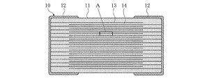
- FIG. 1 is a longitudinal sectional view of a multilayer ceramic capacitor.
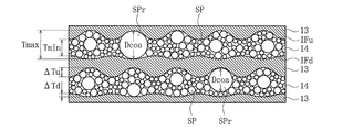
- FIG. 2 is an enlarged view of part A of the multilayer ceramic capacitor shown in FIG. 3 (A) to 3 (F) are explanatory views of a method for manufacturing the multilayer ceramic capacitor shown in FIG.
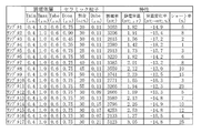
- FIG. 4 is a diagram showing the specifications and characteristics of Samples 1-17.
- FIG. 1 is a longitudinal sectional view of a multilayer ceramic capacitor 10.
- the capacitor body 11 includes a pair of external electrodes 12 provided at both ends in the length direction.
- the capacitor body 11 has a structure in which internal electrode layers 13 and dielectric layers 14 are alternately stacked in the height direction, and only the dielectric layer 14 is stacked in the uppermost portion and the lowermost portion in the height direction. Margin (unsigned) exists.
- Each internal electrode layer 13 has a substantially rectangular shape having a length and width smaller than the length and width of the capacitor body 11, and the left edge of the odd-numbered internal electrode layer 13 from the top in FIG. The right end edge of the even-numbered internal electrode layer 13 is electrically connected to the external electrode 12 on the right side.
- FIG. 1 shows a total of 26 internal electrode layers 13 for convenience of illustration, but the number of the internal electrode layers 13 in the multilayer ceramic capacitor 10 corresponding to miniaturization and large capacity reaches 100 or more.
- each external electrode 12 has a two-layer structure of a base layer made of nickel, copper or the like and a surface layer made of tin, palladium, gold, zinc or the like formed on the surface of the base layer, or A three-layer structure in which an intermediate layer made of platinum, palladium, gold, copper, nickel or the like is interposed between the base layer and the surface layer.
- FIG. 2 is an enlarged view of part A of the multilayer ceramic capacitor 10 shown in FIG. Incidentally, FIG. 2 is based on an image obtained by observing a longitudinal section corresponding to FIG. 1 of Sample 1 to be described later with a scanning electron microscope (Scanning Electron Microscope).
- Each internal electrode layer 13 is composed of metal particles having various particle diameters coupled to each other, and each dielectric layer 14 is composed of ceramic particles SP having various particle diameters coupled to each other.
- the metal particles constituting each internal electrode 13 are composed of at least one kind of particles of nickel, copper, palladium, and silver, and the ceramic particles SP constituting each dielectric layer 14 are composed of barium titanate belonging to a ferroelectric. , Strontium titanate, calcium titanate, magnesium titanate, calcium zirconate, calcium zirconate titanate, barium zirconate, and titanium oxide.
- the ceramic particles SP constituting each dielectric layer 14 have Tmin ⁇ Dcoa ⁇ when the maximum thickness of the dielectric layer 14 is Tmax and the minimum thickness of the dielectric layer 14 is Tmin.
- At least one coarse ceramic particle SPr having a coarse particle diameter Dcoa that satisfies the condition of Tmax is included. If the thickness is smaller than the minimum thickness Tmin of the coarse particle diameter Dcoa of the coarse ceramic particles SPr, it becomes difficult to prevent the deterioration of the electrostatic capacity and the capacity-temperature characteristics, which are the intended problems. Further, since there may be a mode in which the maximum thickness Tmax is substantially the same as the coarse particle diameter Dcoa, as in the coarse ceramic particle SPr at the upper left of FIG. 2, the upper limit value of the coarse particle diameter Dcoa of the coarse ceramic particle SPr is the maximum thickness. It will be called Tmax.
- the ratio of the coarse ceramic particles SPr contained in the ceramic particles SP constituting each dielectric layer 14 is in the range of 25 to 50 vol%, more preferably in the range of 30 to 40 vol%. If the ratio of coarse ceramic particles SPr contained in the ceramic particles SP constituting each dielectric layer 14 is less than 25 vol%, it is difficult to prevent the deterioration of capacitance and capacitance-temperature characteristics, which are intended problems. . Moreover, when the ratio of the coarse ceramic particles SPr included in the ceramic particles SP constituting each dielectric layer 14 exceeds 50 vol%, it is difficult to suppress the occurrence of a short circuit.
- each dielectric layer 14 when the proportion of coarse ceramic particles SPr included in the ceramic particles SP constituting each dielectric layer 14 exceeds 50 vol%, the thickness of each dielectric layer 14 is reduced, that is, the formula of (Tmax + Tmin) / 2, Alternatively, it is difficult to reduce the average thickness Tabe obtained by the equation of Tmin + [( ⁇ Tu + ⁇ Td) / 2].
- the average particle diameter Dbe of the ceramic particles SP (including the coarse ceramic particles SPr) constituting each dielectric layer 14 is 0.15 ⁇ Tabe ⁇ Dab, where the average thickness of each dielectric layer 14 is Tabe.
- the condition of ⁇ 0.3 ⁇ Tabe is satisfied, more preferably the condition of 0.18 ⁇ Tabe ⁇ Dab ⁇ 0.25 ⁇ Tabe is satisfied.
- the average particle diameter Dbe of the ceramic particles SP constituting each dielectric layer 14 is smaller than 0.15 ⁇ Tabe, it is difficult to prevent deterioration of capacitance and capacitance-temperature characteristics, which are intended problems. Further, if the average particle diameter Dbe of the ceramic particles SP constituting each dielectric layer 14 is larger than 0.3 ⁇ Tabe, it is difficult to suppress the occurrence of a short circuit.
- ⁇ Production method of multilayer ceramic capacitor> 3A to 3F show a method for manufacturing the multilayer ceramic capacitor 10 shown in FIG.
- a ceramic slurry and an electrode paste are prepared.
- the ceramic slurry contains at least ceramic particles, a solvent, and a binder, and various additives as necessary.
- the electrode paste includes at least metal particles, a solvent, and a binder, and various additives as necessary.
- Ceramic particles contained in the ceramic slurry may be any one of barium titanate, strontium titanate, calcium titanate, magnesium titanate, calcium zirconate, calcium zirconate titanate, barium zirconate, and titanium oxide belonging to the ferroelectric. It has a predetermined d50 (median diameter) and particle size distribution.
- the solvent is made of at least one of methanol, ethanol, propanol, butanol, ethyl acetate, butyl acetate, toluene, xylene
- the binder is at least one of polyvinyl butyral, acrylic resin, urethane resin, and polyvinyl acetal. It consists of one. Dispersants, plasticizers, leveling agents, etc.
- the dispersants are cationic dispersants, anionic dispersants, nonionic dispersants, amphoteric surfactants, polymer dispersants, etc.
- the plasticizer and leveling agent There are no particular restrictions on the plasticizer and leveling agent, and known ones can be used.
- the metal particles contained in the electrode paste are composed of at least one of nickel, copper, palladium, and silver, and have a predetermined d50 (median diameter) and particle size distribution.
- the solvent is at least one of terpineol ( ⁇ , ⁇ , ⁇ and mixtures thereof), dihydroterpineol, dihydroterpineol acetate, octanol, decanol, tridecanol, butyl carbitol, butyl carbitol acetate, toluene, ethanol.
- the binder is made of at least one of ethyl cellulose, nitrocellulose, acrylic resin, and polyvinyl butyral. Dispersants, plasticizers, leveling agents, etc.
- the dispersants are cationic dispersants, anionic dispersants, nonionic dispersants, amphoteric surfactants, polymer dispersants, etc.
- the plasticizer and leveling agent There are no particular restrictions on the plasticizer and leveling agent, and known ones can be used.
- the ceramic slurry is applied to the upper surface of the base film BF made of polyethylene terephthalate or the like by a coating machine using a doctor blade or a slit die, and the coated material is dried.
- a first lamination sheet in which a slurry layer SL having a predetermined thickness t1 is formed on the base film BF is produced. Ceramic particles having various particle sizes are irregularly arranged in the slurry layer SL.
- the electrode paste is printed on the upper surface of the slurry layer SL of the first laminating sheet by a printing machine using a screen or an intaglio, and the printed matter is dried.
- a second lamination sheet in which a predetermined thickness t2 and a predetermined shape of the paste layer PL is formed in a predetermined arrangement on the slurry layer SL is produced.
- metal particles having various particle sizes are irregularly arranged.
- the slurry layer SL of the first laminating sheet is punched out at a predetermined size, and the punched slurry layer SL is sucked and transported to the flat lower surface of the suction head AH.
- the slurry layer SL is placed on the flat upper surface of the lamination table LT.
- the punched slurry layer SL is sucked and transported to the flat lower surface of the suction head AH, and the operation of thermocompression bonding the slurry layer SL on the upper surface of the slurry layer SL on the stacking table LT is repeated a predetermined number of times. .
- the slurry layer SL of the second laminating sheet is punched out at a predetermined size, and the paste layer PL side of the punched slurry layer SL (including many paste layers PL) is removed.
- the slurry layer SL is sucked and transported to the flat lower surface of the suction head AH, and the slurry layer SL is thermocompression bonded to the upper surface of the thermocompression-bonded slurry layer SL ′.
- the paste layer PL side of the similarly punched slurry layer SL (including a large number of paste layers PL) is sucked and conveyed to the flat lower surface of the suction head AH, and the slurry layer SL is subjected to thermocompression-bonded paste layer PL. Repeat the process of thermocompression bonding over the top surface of 'prescribed times.
- a visible interface appears between the slurry layers SL ′ and the paste layers PL ′ having a predetermined number of layers subjected to thermocompression bonding, which may be of different composition, and the paste
- the rough waveform of the upper interface of the slurry layer SL ′ sandwiched between the layers PL ′ is larger than the rough waveform of the lower interface.
- the reason why such undulations appear is that, in addition to the irregularly arranged ceramic particles having various particle sizes displaced in each slurry layer SL before thermocompression, the punched slurry layer SL has its displacement. Since the paste layer PL side is thermocompression bonded while being sucked to the flat lower surface of the suction head AH, the upper interface of the slurry layer SL is likely to undulate during the thermocompression process.
- the slurry layer SL of the first laminating sheet is punched out at a predetermined size, and the punched slurry layer SL is sucked and transported to the flat lower surface of the suction head AH.
- the slurry layer SL is thermocompression bonded to the upper surface of the paste layer PL ′ that has been thermocompression bonded.
- the punched slurry layer SL is sucked and transported to the flat lower surface of the suction head AH, and the operation of thermocompression bonding the slurry layer SL on the upper surface of the thermobonded slurry layer SL ′ is repeated a predetermined number of times. .
- thermocompression bonding there is no interface between the slurry layers SL ′ having a predetermined number of layers subjected to thermocompression bonding that can be visually recognized because they have the same composition. Since ceramic particles having various particle sizes irregularly arranged in the slurry layer SL are displaced in the thermocompression bonding process, the virtual mutual contact surface (see the broken line) after the thermocompression bonding has undulations.
- thermocompression product is subjected to final thermocompression bonding with a press such as a hot isostatic press to produce a laminate.
- a press such as a hot isostatic press
- the laminate is cut into a lattice shape by a cutting machine such as a dicing machine, and a chip corresponding to the capacitor body 11 shown in FIG. 1 is manufactured.
- a large number of chips are put into a firing furnace and fired (including binder removal treatment) under predetermined conditions.
- the chip Since the fired chip corresponds to the capacitor body 11 shown in FIG. 1, the chip has the internal electrode layer 13 and the dielectric layer 14 shown in FIG.
- the ceramic particles SP constituting the dielectric layer 14 of the chip after firing satisfy the condition of Tmin ⁇ Dcoa ⁇ Tmax (Tmin is the minimum thickness of the dielectric layer 14 and Tmax is the maximum thickness of the dielectric layer 14).
- Tmin is the minimum thickness of the dielectric layer 14
- Tmax is the maximum thickness of the dielectric layer 14.
- the coarse ceramic particles SPr having the coarse particle diameter Dcoa the following two methods can be employed.
- the ceramic particles contained in the ceramic slurry have (1) a particle size distribution containing coarse ceramic particles approximate to the coarse ceramic particles SPr of the coarse particle size Dcoa, for example, a coarse particle size Dcoa around d95. (2) a mixture obtained by adding coarse ceramic particles SPr having a coarse particle diameter Dcoa to ceramic particles having a particle size distribution not containing coarse ceramic particles SPr having a coarse particle diameter Dcoa, and (3) d50 This is a method using a mixture of small ceramic particles and ceramic particles having a large d50 and a coarse particle diameter Dcoa around d95.
- ceramic particles contained in the ceramic slurry ceramic particles having a particle size distribution not containing coarse ceramic particles SPr having a coarse particle size Dcoa are used, and coarse ceramics are formed by grain growth of the ceramic particles in the firing process. This is a method of forming particles SPr.
- the dielectric of the chip after baking is obtained.
- the condition that the coarse particle diameter Dcoa of the coarse ceramic particles SPr included in the ceramic particles SP constituting the body layer 14 is Tmin ⁇ Dcoa ⁇ Tmax (where Tmin is the minimum thickness of the dielectric layer 14 and Tmax is the maximum thickness of the dielectric layer 14).
- Tmin is the minimum thickness of the dielectric layer 14
- Tmax is the maximum thickness of the dielectric layer 14
- the ratio of coarse ceramic particles SPr contained in the ceramic particles SP constituting the dielectric layer 14 of the chip after firing is within the range of 25 to 50 vol%, and firing is further performed.
- the average particle diameter Dbe of the ceramic particles SP included in the ceramic particles SP constituting the dielectric layer 14 of the later chip In order to satisfy the condition of 0.15 ⁇ Tabe ⁇ Dab ⁇ 0.3 ⁇ Tabe (Tabe is the average thickness of the dielectric layer 14), it is necessary to consider the variation of the particle size distribution as necessary. It is desirable to add the same grain growth inhibitor to the ceramic slurry in advance.
- an electrode paste equivalent to the above electrode paste is applied to both ends in the longitudinal direction of the chip after baking by a coating machine such as a dip coating machine or a roller coating machine, and the coated material is subjected to a baking treatment.
- the base layer of the external electrode 12 shown in 1 is formed.
- a surface layer is formed on the surface of the underlayer by a plating method such as electrolytic plating to produce the external electrode 12 having a two-layer structure.
- the intermediate layer and the surface layer are sequentially formed on the surface of the base layer by a plating method such as electrolytic plating to produce the external electrode 12 having a three-layer structure.
- ⁇ Sample 1> Standard dimensions of capacitor body: length 1.0mm, width 0.5mm, height 0.2mm ⁇ Internal electrode layer ⁇ Average thickness: 0.7 ⁇ m ⁇ Number of layers: 100 ⁇ Metal particles: Nickel ⁇ Average particle size: 0.2 ⁇ m ⁇ Dielectric layer ⁇ Minimum thickness Tmin: 0.4 ⁇ m ⁇ Maximum thickness Tmax: 1.0 ⁇ m ⁇ Average thickness Tabe: 0.6 ⁇ m ⁇ Number of layers: 100 Ceramic particles SP: barium titanate Coarse particle diameter Dcoa: 0.75 ⁇ m Average particle size Dab: 0.11 ⁇ m -Ratio of coarse ceramic particles: 30 vol% ⁇ Sample 2> Same as Sample 1 except that the coarse particle size Dcoa is 0.90 ⁇ m.
- Example 13 Same as Sample 1, except that the average particle size Dab is 0.13 ⁇ m.
- Example 15 Same as Sample 1, except that the average particle size Dab is 0.17 ⁇ m.
- Example 17 Same as Sample 1, except that the average particle size Dab is 0.21 ⁇ m.
- FIG. 4 shows the specifications and characteristics of the samples 1 to 17, and a method for measuring the specifications and characteristics shown in the figure will be described below.
- 10 samples 1 to 17 are prepared for each of Tmin (minimum thickness), Tmax (maximum thickness), and Tabe (average thickness) of the dielectric layer in each sample 1 to 17, and each of the longitudinal sections corresponding to FIG.
- the surface was observed with a scanning electron microscope (Scanning Electron Microscope) at a magnification of 3000 times, and Tmin (minimum thickness) and Tmax (maximum thickness) of the dielectric layer within the observation range were measured, respectively.
- the average value of Tmin (minimum thickness) and the average value of 10 Tmax (maximum thickness) are set as Tmin (minimum thickness) and Tmax (maximum thickness) of samples 1 to 17, respectively.
- the average thickness obtained using (minimum thickness) and Tmax (maximum thickness) was defined as the Tabe (average thickness) of each of Samples 1 to 17.
- Dcoa (coarse particle diameter), ratio, and Dave (average particle diameter) of the ceramic particles in each of samples 1 to 17 were measured by measuring the particle diameters of all the ceramic particles within the observation range.
- the particle size of all ceramic particles in another observation range is continuously measured so that the number of measurement becomes 300 or more, and then Dcoa (coarse particle size) And the volume ratio and Dave (average particle diameter) of the coarse particles based on the cross-sectional area thereof, respectively, the average value of 10 Dcoa (coarse particle diameter), the average value of 10 volume ratios, and 10 Dave ( The average value of the average particle diameter was defined as Dcoa (coarse particle diameter), ratio, and Dave (average particle diameter) of each of samples 1 to 17.
- the dielectric constant, capacitance, and capacitance change rate of each sample 1 to 17 were prepared for 10 samples 1 to 17 individually, and the dielectric constant of the dielectric layer in a 25 ° C. atmosphere at a frequency of 1 KHz and a voltage of 1 V. The total capacitance is measured again, and the total capacitance is again measured in an atmosphere of 85 ° C. The capacitance change rate (capacity reduction rate) with respect to the temperature change from 25 ° C. to 85 ° C. is expressed as a percentage. The average value of 10 dielectric constants, the average value of 10 electrostatic capacitances, and the average value of 10 capacitance change rates were used as the dielectric constant, capacitance, and capacitance change rate of each of samples 1 to 17, respectively. .
- the short-circuit ratio of the characteristics in each sample 1 to 17 was prepared individually for each of samples 1 to 17, and those having a resistance value of less than 1 K ⁇ at a DC voltage of 1 V were short-circuited. The number expressed as a percentage was taken as the short rate for each of Samples 1-17.
- the capacitances of Samples 1 to 3 in which the coarse particle diameter Dcoa of the coarse ceramic particles SPr included in the ceramic particles SP constituting the dielectric layer 14 satisfy the condition of Tmin ⁇ Dcoa ⁇ Tmax are as follows:
- the coarse particle diameter Dcoa is higher than the electrostatic capacity of sample 4 that does not satisfy the same condition, and the capacity change rate (capacitance temperature characteristics) of samples 1 to 3 is the same as that of sample 4 in which coarse particle diameter Dcoa does not satisfy the same condition. It is superior to the capacity change rate (capacitance temperature characteristic) (within ⁇ 18%).
- the capacitances of Samples 1 and 5 to 9 in which the ratio of coarse ceramic particles SPr contained in the ceramic particles SP constituting the dielectric layer 14 is in the range of 25 to 50 vol% are as follows: The ratio of the coarse ceramic particles SPr is higher than the capacitance of the sample 10 outside the same range, and the short ratio of the samples 1 and 5 to 9 is the short ratio of the sample 11 where the ratio of the coarse ceramic particles SPr is outside the same range. Lower than (15% or less).
- the rate of change in capacity (capacitance temperature characteristics) of the samples 1, 6 and 7 in which the ratio of the coarse ceramic particles SPr is in the range of 30 to 40 vol% is the ratio of the coarse ceramic particles SPr. It is superior to the capacity change rate (capacitance temperature characteristic) of sample 5 outside the same range (within ⁇ 15%), and the short ratio of samples 1, 6 and 7 is the same as the ratio of coarse ceramic particles SPr. It is lower than the short-circuit rate of samples 8 and 9 that come off (8% or less).
- the condition that the average particle diameter Dbe of the ceramic particles SP constituting the dielectric layer 14 is 0.15 ⁇ Tabe ⁇ Dab ⁇ 0.3 ⁇ Tabe (here 0.09 ⁇ m ⁇ Dab ⁇ 0).
- the capacitance of samples 1 and 12 to 15 satisfying .18 ⁇ m) is higher than the capacitance of sample 16 whose average particle diameter Dbe does not satisfy the same conditions, and the short-circuit rate of samples 1 and 12 to 15 is The average particle diameter Dbe is lower (12% or less) than the short-circuit rate of Sample 17 that does not satisfy the same condition.
- Samples 1 and 12 to 15 Samples 1 and 13 satisfying the condition that the average particle size Dave is 0.18 ⁇ Tabe ⁇ Dab ⁇ 0.25 ⁇ Tabe (here, 0.108 ⁇ m ⁇ Dab ⁇ 0.15 ⁇ m). 14 and the capacity change rate (capacitance-temperature characteristics) of the sample 14 are superior to the capacity change rate (capacitance-temperature characteristics) of the sample 12 in which the average particle diameter Dab does not satisfy the same conditions (within ⁇ 15%), and the sample 1 , 13 and 14 are lower (10% or less) than the short-circuit rate of sample 15 in which the average particle diameter Dbe does not satisfy the same condition.
- SYMBOLS 10 Multilayer ceramic capacitor, 11 ... Capacitor main body, 12 ... External electrode, 13 ... Internal electrode layer, 14 ... Dielectric layer, SP ... Ceramic particle, SPr ... Coarse ceramic particle.
Landscapes
- Engineering & Computer Science (AREA)
- Power Engineering (AREA)
- Chemical & Material Sciences (AREA)
- Ceramic Engineering (AREA)
- Manufacturing & Machinery (AREA)
- Microelectronics & Electronic Packaging (AREA)
- Inorganic Chemistry (AREA)
- Fixed Capacitors And Capacitor Manufacturing Machines (AREA)
- Ceramic Capacitors (AREA)
Description
図1は、積層セラミックコンデンサ10の縦断面図を示す。この積層セラミックコンデンサ10は、長さ、幅及び高さの基準寸法が長さ>幅=高さの関係、或いは、長さ>幅>高さの関係を有する略直方体形状のコンデンサ本体11と、該コンデンサ本体11の長さ方向両端部に設けられた1対の外部電極12とを備えている。
図2は、図1に示した積層セラミックコンデンサ10のA部拡大図を示す。因みに、この図2は、後記サンプル1の図1対応の縦断面を走査型電子顕微鏡(Scanning Electron Microscope)で観察して得た画像に基づいている。
図3(A)~図3(F)は、図1に示した積層セラミックコンデンサ10の製法を示す。製造に際しては、先ず、セラミックスラリーと電極ペーストを用意する。セラミックスラリーは、セラミック粒子と溶剤とバインダを少なくとも含み、必要に応じて各種添加剤を含む。また、電極ペーストは、金属粒子と溶剤とバインダを少なくとも含み、必要に応じて各種添加剤を含む。
図1及び図2に示した積層セラミックコンデンサ10によって得られる効果を検証するために、下記サンプル1~17(積層セラミックコンデンサ)を前記《積層セラミックコンデンサの製法》に準じて各々120個ずつ製造した。
・コンデンサ本体の基準寸法 :長さ1.0mm、幅0.5mm、高さ0.2mm
・内部電極層
・平均厚さ :0.7μm
・層数 :100
・金属粒子 :ニッケル
・平均粒子径 :0.2μm
・誘電体層
・最小厚さTmin :0.4μm
・最大厚さTmax :1.0μm
・平均厚さTabe :0.6μm
・層数 :100
・セラミック粒子SP :チタン酸バリウム
・粗大粒子径Dcoa :0.75μm
・平均粒子径Dabe :0.11μm
・粗大セラミック粒子の割合:30vol%
〈サンプル2〉
粗大粒子径Dcoaが0.90μmである以外は、サンプル1と同じ。
粗大粒子径Dcoaが0.45μmである以外は、サンプル1と同じ。
粗大粒子径Dcoaが0.35μmである以外は、サンプル1と同じ。
粗大セラミック粒子の割合が25vol%である以外は、サンプル1と同じ。
粗大セラミック粒子の割合が35vol%である以外は、サンプル1と同じ。
粗大セラミック粒子の割合が40vol%である以外は、サンプル1と同じ。
粗大セラミック粒子の割合が45vol%である以外は、サンプル1と同じ。
粗大セラミック粒子の割合が50vol%である以外は、サンプル1と同じ。
粗大セラミック粒子の割合が20vol%である以外は、サンプル1と同じ。
粗大セラミック粒子の割合が55vol%である以外は、サンプル1と同じ。
平均粒子径Dabeが0.09μmである以外は、サンプル1と同じ。
平均粒子径Dabeが0.13μmである以外は、サンプル1と同じ。
平均粒子径Dabeが0.15μmである以外は、サンプル1と同じ。
平均粒子径Dabeが0.17μmである以外は、サンプル1と同じ。
平均粒子径Dabeが0.07μmである以外は、サンプル1と同じ。
平均粒子径Dabeが0.21μmである以外は、サンプル1と同じ。
Claims (3)
- 相互結合した種々粒子径の金属粒子によって構成された内部電極層と、相互結合した種々粒子径のセラミック粒子によって構成された誘電体層が、交互に積層された構造を有する積層セラミックコンデンサであって、
前記誘電体層を構成するセラミック粒子は、前記誘電体層の最大厚さをTmaxとし、前記誘電体層の最小厚さをTminとしたとき、Tmin≦Dcoa≦Tmaxの条件を満足する粗大粒子径Dcoaの粗大セラミック粒子を含む、
ことを特徴とする積層セラミックコンデンサ。 - 前記誘電体層を構成するセラミック粒子に含まれる前記粗大セラミック粒子の割合は、25~50vol%の範囲内にある、
ことを特徴とする請求項1に記載の積層セラミックコンデンサ。 - 前記誘電体層を構成するセラミック粒子の平均粒子径Dabeは、前記誘電体層の平均厚さをTabeとしたとき、0.15×Tabe≦Dabe≦0.3×Tabeの条件を満足する、
ことを特徴とする請求項1または2に記載の積層セラミックコンデンサ。
Priority Applications (4)
| Application Number | Priority Date | Filing Date | Title |
|---|---|---|---|
| KR1020157005156A KR101571667B1 (ko) | 2012-03-07 | 2013-03-06 | 적층 세라믹 콘덴서 |
| US14/234,954 US9418792B2 (en) | 2012-03-07 | 2013-03-06 | Multilayer ceramic capacitor |
| CN201380002427.9A CN103718260B (zh) | 2012-03-07 | 2013-03-06 | 层叠陶瓷电容器 |
| KR1020137033458A KR101524522B1 (ko) | 2012-03-07 | 2013-03-06 | 적층 세라믹 콘덴서 |
Applications Claiming Priority (2)
| Application Number | Priority Date | Filing Date | Title |
|---|---|---|---|
| JP2012-050106 | 2012-03-07 | ||
| JP2012050106A JP5450696B2 (ja) | 2012-03-07 | 2012-03-07 | 積層セラミックコンデンサ |
Publications (1)
| Publication Number | Publication Date |
|---|---|
| WO2013133304A1 true WO2013133304A1 (ja) | 2013-09-12 |
Family
ID=49116777
Family Applications (1)
| Application Number | Title | Priority Date | Filing Date |
|---|---|---|---|
| PCT/JP2013/056091 Ceased WO2013133304A1 (ja) | 2012-03-07 | 2013-03-06 | 積層セラミックコンデンサ |
Country Status (5)
| Country | Link |
|---|---|
| US (1) | US9418792B2 (ja) |
| JP (1) | JP5450696B2 (ja) |
| KR (2) | KR101524522B1 (ja) |
| CN (1) | CN103718260B (ja) |
| WO (1) | WO2013133304A1 (ja) |
Families Citing this family (16)
| Publication number | Priority date | Publication date | Assignee | Title |
|---|---|---|---|---|
| JP5462962B1 (ja) * | 2013-01-31 | 2014-04-02 | 太陽誘電株式会社 | 積層セラミックコンデンサ |
| US10431508B2 (en) | 2015-07-19 | 2019-10-01 | Vq Research, Inc. | Methods and systems to improve printed electrical components and for integration in circuits |
| US10128047B2 (en) * | 2015-07-19 | 2018-11-13 | Vq Research, Inc. | Methods and systems for increasing surface area of multilayer ceramic capacitors |
| JP2017174945A (ja) * | 2016-03-23 | 2017-09-28 | 京セラ株式会社 | 積層型電子部品 |
| JP6978862B2 (ja) * | 2017-06-26 | 2021-12-08 | 太陽誘電株式会社 | 積層セラミックコンデンサ |
| US11145458B2 (en) | 2018-02-22 | 2021-10-12 | Taiyo Yuden Co., Ltd. | Multi-layer ceramic electronic component |
| JP7290914B2 (ja) * | 2018-02-26 | 2023-06-14 | 太陽誘電株式会社 | 積層セラミックコンデンサの製造方法 |
| KR102527709B1 (ko) * | 2018-11-09 | 2023-05-02 | 삼성전기주식회사 | 적층 세라믹 전자부품 |
| JP2020184555A (ja) * | 2019-04-26 | 2020-11-12 | 株式会社村田製作所 | 積層セラミックコンデンサ |
| KR102748942B1 (ko) | 2019-07-29 | 2025-01-02 | 삼성전기주식회사 | 적층형 전자 부품 |
| KR102099555B1 (ko) | 2019-11-25 | 2020-04-09 | 주식회사 네이처모빌리티 | 접이식 헬멧 |
| KR102142990B1 (ko) | 2020-01-03 | 2020-08-10 | 주식회사 네이처모빌리티 | 가변형 헬멧 |
| CN115210832A (zh) * | 2020-02-27 | 2022-10-18 | 京瓷株式会社 | 电容器 |
| DE102020002881A1 (de) * | 2020-05-13 | 2021-11-18 | Giesecke+Devrient Currency Technology Gmbh | Gedruckter Folienkondensator mit gesintertem Dielektrikum |
| JP7606330B2 (ja) * | 2020-11-25 | 2024-12-25 | Tdk株式会社 | 積層電子部品 |
| JP7821569B2 (ja) * | 2020-12-16 | 2026-02-27 | 太陽誘電株式会社 | 積層セラミックコンデンサおよび積層セラミックコンデンサの製造方法 |
Citations (2)
| Publication number | Priority date | Publication date | Assignee | Title |
|---|---|---|---|---|
| JP2005123253A (ja) * | 2003-10-14 | 2005-05-12 | Tdk Corp | 積層型セラミックコンデンサ及びその製造方法 |
| JP2008078516A (ja) * | 2006-09-25 | 2008-04-03 | Kyocera Corp | 積層セラミックコンデンサおよびその製法 |
Family Cites Families (13)
| Publication number | Priority date | Publication date | Assignee | Title |
|---|---|---|---|---|
| JP3370933B2 (ja) * | 1998-05-01 | 2003-01-27 | 太陽誘電株式会社 | 積層セラミックコンデンサ |
| US7354642B2 (en) * | 2000-02-16 | 2008-04-08 | Taiyo Yuden Co., Ltd. | Multilayer displacement element |
| JP4471453B2 (ja) * | 2000-05-30 | 2010-06-02 | 京セラ株式会社 | 積層型電子部品 |
| JP3875832B2 (ja) * | 2000-10-17 | 2007-01-31 | Tdk株式会社 | 電子部品およびその製造方法 |
| US6600645B1 (en) * | 2002-09-27 | 2003-07-29 | Ut-Battelle, Llc | Dielectric composite materials and method for preparing |
| JP3908715B2 (ja) | 2003-10-24 | 2007-04-25 | Tdk株式会社 | 積層セラミックコンデンサ |
| JP2005159224A (ja) * | 2003-11-28 | 2005-06-16 | Tdk Corp | 積層セラミックコンデンサ |
| JP4407299B2 (ja) * | 2004-01-30 | 2010-02-03 | Tdk株式会社 | 積層セラミックコンデンサ |
| JP4475425B2 (ja) | 2006-03-24 | 2010-06-09 | Tdk株式会社 | 積層セラミックコンデンサ |
| JP4983102B2 (ja) * | 2006-06-06 | 2012-07-25 | Tdk株式会社 | 誘電体素子 |
| KR101064243B1 (ko) * | 2006-11-29 | 2011-09-14 | 쿄세라 코포레이션 | 적층 세라믹 콘덴서 |
| KR101872520B1 (ko) * | 2011-07-28 | 2018-06-29 | 삼성전기주식회사 | 적층 세라믹 전자부품 |
| KR101862396B1 (ko) * | 2011-09-08 | 2018-05-30 | 삼성전기주식회사 | 적층 세라믹 전자부품 및 이의 제조방법 |
-
2012
- 2012-03-07 JP JP2012050106A patent/JP5450696B2/ja active Active
-
2013
- 2013-03-06 WO PCT/JP2013/056091 patent/WO2013133304A1/ja not_active Ceased
- 2013-03-06 CN CN201380002427.9A patent/CN103718260B/zh active Active
- 2013-03-06 KR KR1020137033458A patent/KR101524522B1/ko active Active
- 2013-03-06 KR KR1020157005156A patent/KR101571667B1/ko active Active
- 2013-03-06 US US14/234,954 patent/US9418792B2/en active Active
Patent Citations (2)
| Publication number | Priority date | Publication date | Assignee | Title |
|---|---|---|---|---|
| JP2005123253A (ja) * | 2003-10-14 | 2005-05-12 | Tdk Corp | 積層型セラミックコンデンサ及びその製造方法 |
| JP2008078516A (ja) * | 2006-09-25 | 2008-04-03 | Kyocera Corp | 積層セラミックコンデンサおよびその製法 |
Also Published As
| Publication number | Publication date |
|---|---|
| CN103718260B (zh) | 2017-03-08 |
| KR101571667B1 (ko) | 2015-11-25 |
| US20140254063A1 (en) | 2014-09-11 |
| JP2013187280A (ja) | 2013-09-19 |
| JP5450696B2 (ja) | 2014-03-26 |
| US9418792B2 (en) | 2016-08-16 |
| KR20140016978A (ko) | 2014-02-10 |
| CN103718260A (zh) | 2014-04-09 |
| KR101524522B1 (ko) | 2015-06-01 |
| KR20150036780A (ko) | 2015-04-07 |
Similar Documents
| Publication | Publication Date | Title |
|---|---|---|
| JP5450696B2 (ja) | 積層セラミックコンデンサ | |
| JP5362033B2 (ja) | 積層型セラミックコンデンサ | |
| KR101843182B1 (ko) | 적층 세라믹 전자부품 | |
| KR101946259B1 (ko) | 적층 세라믹 전자부품 | |
| JP6138442B2 (ja) | 積層セラミック電子部品及びその製造方法 | |
| US20130063862A1 (en) | Multilayer ceramic electronic component and fabrication method thereof | |
| US20080305944A1 (en) | Dielectric ceramics and manufacturing method thereof, as well as multilayer ceramic capacitor | |
| JP2013149936A (ja) | 積層セラミック電子部品及びその製造方法 | |
| JP7283357B2 (ja) | 積層セラミックコンデンサ | |
| JP6869677B2 (ja) | 積層セラミックコンデンサおよびその製造方法 | |
| KR101792275B1 (ko) | 내부 전극용 도전성 페이스트, 이를 포함하는 적층 세라믹 전자 부품 및 그 제조 방법 | |
| JP5414940B1 (ja) | 積層セラミックコンデンサ | |
| JP2019102655A (ja) | セラミックコンデンサおよびその製造方法 | |
| JP5532460B2 (ja) | 積層セラミック電子部品 | |
| KR20240104031A (ko) | 적층 세라믹 전자 부품, 및 적층 세라믹 전자 부품의 제조 방법 | |
| JP7493322B2 (ja) | 積層セラミックコンデンサ | |
| JP2014057098A (ja) | 積層セラミックコンデンサ | |
| CN104620341B (zh) | 层叠陶瓷电容器 | |
| JP5501392B2 (ja) | 積層セラミックコンデンサ | |
| TWI587334B (zh) | 積層陶瓷電容器 | |
| JP2014103422A (ja) | 積層セラミックコンデンサ |
Legal Events
| Date | Code | Title | Description |
|---|---|---|---|
| 121 | Ep: the epo has been informed by wipo that ep was designated in this application |
Ref document number: 13758316 Country of ref document: EP Kind code of ref document: A1 |
|
| ENP | Entry into the national phase |
Ref document number: 20137033458 Country of ref document: KR Kind code of ref document: A |
|
| WWE | Wipo information: entry into national phase |
Ref document number: 14234954 Country of ref document: US |
|
| NENP | Non-entry into the national phase |
Ref country code: DE |
|
| 122 | Ep: pct application non-entry in european phase |
Ref document number: 13758316 Country of ref document: EP Kind code of ref document: A1 |