WO2013133104A1 - 電力変換装置 - Google Patents
電力変換装置 Download PDFInfo
- Publication number
- WO2013133104A1 WO2013133104A1 PCT/JP2013/055144 JP2013055144W WO2013133104A1 WO 2013133104 A1 WO2013133104 A1 WO 2013133104A1 JP 2013055144 W JP2013055144 W JP 2013055144W WO 2013133104 A1 WO2013133104 A1 WO 2013133104A1
- Authority
- WO
- WIPO (PCT)
- Prior art keywords
- power
- substrate
- bus bar
- conversion device
- power module
- Prior art date
- Legal status (The legal status is an assumption and is not a legal conclusion. Google has not performed a legal analysis and makes no representation as to the accuracy of the status listed.)
- Ceased
Links
Images












Classifications
-
- H—ELECTRICITY
- H05—ELECTRIC TECHNIQUES NOT OTHERWISE PROVIDED FOR
- H05K—PRINTED CIRCUITS; CASINGS OR CONSTRUCTIONAL DETAILS OF ELECTRIC APPARATUS; MANUFACTURE OF ASSEMBLAGES OF ELECTRICAL COMPONENTS
- H05K1/00—Printed circuits
- H05K1/02—Details
- H05K1/0271—Arrangements for reducing stress or warp in rigid printed circuit boards, e.g. caused by loads, vibrations or differences in thermal expansion
-
- H—ELECTRICITY
- H02—GENERATION; CONVERSION OR DISTRIBUTION OF ELECTRIC POWER
- H02M—APPARATUS FOR CONVERSION BETWEEN AC AND AC, BETWEEN AC AND DC, OR BETWEEN DC AND DC, AND FOR USE WITH MAINS OR SIMILAR POWER SUPPLY SYSTEMS; CONVERSION OF DC OR AC INPUT POWER INTO SURGE OUTPUT POWER; CONTROL OR REGULATION THEREOF
- H02M7/00—Conversion of AC power input into DC power output; Conversion of DC power input into AC power output
- H02M7/003—Constructional details, e.g. physical layout, assembly, wiring or busbar connections
-
- H—ELECTRICITY
- H02—GENERATION; CONVERSION OR DISTRIBUTION OF ELECTRIC POWER
- H02M—APPARATUS FOR CONVERSION BETWEEN AC AND AC, BETWEEN AC AND DC, OR BETWEEN DC AND DC, AND FOR USE WITH MAINS OR SIMILAR POWER SUPPLY SYSTEMS; CONVERSION OF DC OR AC INPUT POWER INTO SURGE OUTPUT POWER; CONTROL OR REGULATION THEREOF
- H02M7/00—Conversion of AC power input into DC power output; Conversion of DC power input into AC power output
- H02M7/42—Conversion of DC power input into AC power output without possibility of reversal
- H02M7/44—Conversion of DC power input into AC power output without possibility of reversal by static converters
- H02M7/48—Conversion of DC power input into AC power output without possibility of reversal by static converters using discharge tubes with control electrode or semiconductor devices with control electrode
- H02M7/53—Conversion of DC power input into AC power output without possibility of reversal by static converters using discharge tubes with control electrode or semiconductor devices with control electrode using devices of a triode or transistor type requiring continuous application of a control signal
- H02M7/537—Conversion of DC power input into AC power output without possibility of reversal by static converters using discharge tubes with control electrode or semiconductor devices with control electrode using devices of a triode or transistor type requiring continuous application of a control signal using semiconductor devices only, e.g. single switched pulse inverters
-
- H—ELECTRICITY
- H05—ELECTRIC TECHNIQUES NOT OTHERWISE PROVIDED FOR
- H05K—PRINTED CIRCUITS; CASINGS OR CONSTRUCTIONAL DETAILS OF ELECTRIC APPARATUS; MANUFACTURE OF ASSEMBLAGES OF ELECTRICAL COMPONENTS
- H05K1/00—Printed circuits
- H05K1/18—Printed circuits structurally associated with non-printed electric components
- H05K1/181—Printed circuits structurally associated with non-printed electric components associated with surface mounted components
-
- H—ELECTRICITY
- H05—ELECTRIC TECHNIQUES NOT OTHERWISE PROVIDED FOR
- H05K—PRINTED CIRCUITS; CASINGS OR CONSTRUCTIONAL DETAILS OF ELECTRIC APPARATUS; MANUFACTURE OF ASSEMBLAGES OF ELECTRICAL COMPONENTS
- H05K2201/00—Indexing scheme relating to printed circuits covered by H05K1/00
- H05K2201/10—Details of components or other objects attached to or integrated in a printed circuit board
- H05K2201/10007—Types of components
- H05K2201/10015—Non-printed capacitor
-
- H—ELECTRICITY
- H05—ELECTRIC TECHNIQUES NOT OTHERWISE PROVIDED FOR
- H05K—PRINTED CIRCUITS; CASINGS OR CONSTRUCTIONAL DETAILS OF ELECTRIC APPARATUS; MANUFACTURE OF ASSEMBLAGES OF ELECTRICAL COMPONENTS
- H05K2201/00—Indexing scheme relating to printed circuits covered by H05K1/00
- H05K2201/10—Details of components or other objects attached to or integrated in a printed circuit board
- H05K2201/10007—Types of components
- H05K2201/10037—Printed or non-printed battery
-
- H—ELECTRICITY
- H05—ELECTRIC TECHNIQUES NOT OTHERWISE PROVIDED FOR
- H05K—PRINTED CIRCUITS; CASINGS OR CONSTRUCTIONAL DETAILS OF ELECTRIC APPARATUS; MANUFACTURE OF ASSEMBLAGES OF ELECTRICAL COMPONENTS
- H05K2201/00—Indexing scheme relating to printed circuits covered by H05K1/00
- H05K2201/10—Details of components or other objects attached to or integrated in a printed circuit board
- H05K2201/10007—Types of components
- H05K2201/10151—Sensor
-
- H—ELECTRICITY
- H05—ELECTRIC TECHNIQUES NOT OTHERWISE PROVIDED FOR
- H05K—PRINTED CIRCUITS; CASINGS OR CONSTRUCTIONAL DETAILS OF ELECTRIC APPARATUS; MANUFACTURE OF ASSEMBLAGES OF ELECTRICAL COMPONENTS
- H05K2201/00—Indexing scheme relating to printed circuits covered by H05K1/00
- H05K2201/10—Details of components or other objects attached to or integrated in a printed circuit board
- H05K2201/10007—Types of components
- H05K2201/10174—Diode
-
- H—ELECTRICITY
- H05—ELECTRIC TECHNIQUES NOT OTHERWISE PROVIDED FOR
- H05K—PRINTED CIRCUITS; CASINGS OR CONSTRUCTIONAL DETAILS OF ELECTRIC APPARATUS; MANUFACTURE OF ASSEMBLAGES OF ELECTRICAL COMPONENTS
- H05K2201/00—Indexing scheme relating to printed circuits covered by H05K1/00
- H05K2201/10—Details of components or other objects attached to or integrated in a printed circuit board
- H05K2201/10227—Other objects, e.g. metallic pieces
- H05K2201/10272—Busbars, i.e. thick metal bars mounted on the printed circuit board [PCB] as high-current conductors
-
- H—ELECTRICITY
- H05—ELECTRIC TECHNIQUES NOT OTHERWISE PROVIDED FOR
- H05K—PRINTED CIRCUITS; CASINGS OR CONSTRUCTIONAL DETAILS OF ELECTRIC APPARATUS; MANUFACTURE OF ASSEMBLAGES OF ELECTRICAL COMPONENTS
- H05K7/00—Constructional details common to different types of electric apparatus
- H05K7/20—Modifications to facilitate cooling, ventilating, or heating
- H05K7/2089—Modifications to facilitate cooling, ventilating, or heating for power electronics, e.g. for inverters for controlling motor
- H05K7/209—Heat transfer by conduction from internal heat source to heat radiating structure
Definitions
- This invention relates to the power converter device which converts the electric energy with a semiconductor element.
- a power conversion device used for inverter control of an electric motor or the like includes a power semiconductor such as a switching element and a control circuit that controls the operation of the power semiconductor device. Since power semiconductors generate a lot of heat, it is necessary to configure so that the control circuit is not affected by the heat.
- JP4609504B has a second circuit board on which a circuit component for controlling the power semiconductor element is mounted in a vertical direction with respect to the first circuit board on which the power semiconductor element is mounted. , One end of which is electrically joined to a first circuit board is disclosed.
- the second circuit board is connected to the first circuit board on which the power semiconductor element is mounted only at one end side thereof, so that an external such as vibration or impact Stress is generated in the first circuit board and the second circuit board due to the stress from.
- This stress has a problem that the durability reliability of the power converter is lowered.
- This invention is made in view of such a problem, and it aims at providing the power converter device which can improve durability in a power converter device provided with a power semiconductor element.
- a power module including a power semiconductor, a base including a cooler for cooling the power module, a control board on which a control circuit for controlling the power module is mounted, and supplying power to the power module
- Power converter comprising: a first bus bar that performs output; a second bus bar that outputs power from the power module; a smoothing capacitor that smoothes the power of the first bus bar; and a first substrate that includes signal wiring.
- the power module is mounted on the upper surface of the base, and the first bus bar, the smoothing capacitor, and the first substrate are sequentially stacked on the upper side of the power module,
- the control board is provided in a standing direction with respect to the base, and is fixed to the power module and the first board, respectively.
- FIG. 1 is an explanatory diagram of a drive system including a semiconductor module according to the first embodiment of the present invention.
- FIG. 2A is an explanatory diagram of the power conversion device according to the first embodiment of this invention.
- FIG. 2B is an explanatory diagram of the power conversion apparatus according to the first embodiment of this invention.
- FIG. 3A is an explanatory diagram of the power conversion device according to the first embodiment of the present invention, and shows a cross-sectional view in FIG. 2A.
- FIG. 3B is an explanatory diagram of the power conversion device according to the first embodiment of the present invention, and shows a cross-sectional view in FIG. 2A.
- FIG. 4 is an explanatory diagram of the power conversion apparatus according to the second embodiment of this invention.
- FIG. 5A is an explanatory diagram of the power conversion device according to the second embodiment of the present invention, and shows a cross-sectional view in FIG. 4.
- FIG. 5B is an explanatory diagram of the power conversion device according to the second embodiment of the present invention, and shows a cross-sectional view in FIG. 4.
- FIG. 6 is an explanatory diagram of the power conversion device according to the third embodiment of the present invention.
- FIG. 7A is an explanatory diagram of the power conversion device according to the third embodiment of the present invention, and shows a cross-sectional view in FIG. 6.
- FIG. 7B is an explanatory diagram of the power conversion device according to the third embodiment of the present invention, and shows a cross-sectional view in FIG. 6.
- FIG. 8 is an explanatory diagram of the power conversion device according to the fourth embodiment of the present invention.
- FIG. 9A is an explanatory diagram of the power conversion device according to the fourth embodiment of the present invention, and shows a cross-sectional view in FIG. 8.
- FIG. 9B is an explanatory diagram of the power conversion device according to the fourth embodiment of the present invention, and shows a cross-sectional view in FIG. 8.
- FIG. 10 is an explanatory diagram of the power conversion device according to the fifth embodiment of the present invention.
- FIG. 11A is an explanatory diagram of the power converter according to the fifth embodiment of the present invention, and shows a cross-sectional view in FIG. FIG.
- FIG. 11B is an explanatory diagram of the power conversion device according to the fifth embodiment of the present invention, and shows a cross-sectional view in FIG. 10.
- FIG. 12 is an explanatory diagram of the power conversion apparatus according to the sixth embodiment of the present invention.
- FIG. 13A is an explanatory diagram of the power conversion device according to the sixth embodiment of the present invention, and shows a cross-sectional view in FIG. 12.
- FIG. 13B is an explanatory diagram of the power conversion apparatus according to the sixth embodiment of the present invention, and shows a cross-sectional view in FIG. 12.
- FIG. 14 is an explanatory diagram of the power conversion device according to the seventh embodiment of this invention.
- FIG. 15A is an explanatory diagram of the power conversion device according to the seventh embodiment of the present invention, and shows a cross-sectional view in FIG. 14.
- FIG. 15B is an explanatory diagram of the power conversion device according to the seventh embodiment of the present invention, and shows a cross-sectional view in FIG. 14.
- FIG. 16 is an explanatory diagram of the power conversion device according to the eighth embodiment of the present invention.
- FIG. 17A is an explanatory diagram of the power conversion device according to the eighth embodiment of the present invention, and shows a cross-sectional view in FIG. 16.
- FIG. 17B is an explanatory diagram of the power conversion device according to the eighth embodiment of the present invention, and shows a cross-sectional view in FIG. 16.
- FIG. 18 is an explanatory diagram of the power conversion device according to the ninth embodiment of this invention.
- FIG. 19A is an explanatory diagram of the power converter according to the ninth embodiment of the present invention, and shows a cross-sectional view in FIG.
- FIG. 19B is an explanatory diagram of the power conversion device according to the ninth embodiment of the present invention, and shows a cross-sectional view in FIG. 18.
- FIG. 1 is an explanatory diagram of the drive system 1 according to the first embodiment of the present invention.
- the drive system 1 includes a power conversion device 50, a battery 20, and a drive motor M.
- the power conversion device 50 includes a control circuit 10, a power semiconductor 31, a diode 32, a smoothing capacitor 40, and the like, and controls the drive motor M by controlling the output of the power semiconductor 31 by the control circuit 10.
- the battery 20 supplies power to the drive motor M and stores regenerative power of the drive motor M.
- the battery 20 is configured as a battery module in which a plurality of secondary batteries such as a lead battery, a nickel metal hydride battery, or a lithium ion battery are connected in series or in parallel.
- the power semiconductor 31 is configured by a semiconductor element such as an IGBT.
- the diode 32 is configured by a semiconductor element such as a fast recovery diode (FRD).
- FPD fast recovery diode
- the diode 32 protects the power semiconductor 31 by preventing reverse current from being applied to the power semiconductor 31.
- the smoothing capacitor 40 smoothes the output power of the power semiconductor 31.
- the control circuit 10 applies a gate current to each power semiconductor 31 when increasing the output of the driving motor M, for example. Thereby, a high current from the battery 20 is supplied to the drive motor M.
- the control circuit 10 controls the output of the driving motor M by controlling the gate current by the duty ratio or the like. During regeneration of the drive motor M, power is regenerated to the battery 20 via the power converter 50.
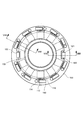
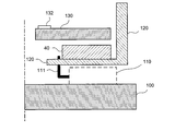
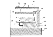
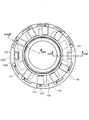
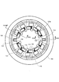
- FIG. 2A, 2B, 3A, and 3B are explanatory diagrams of the power conversion device 50 according to the first embodiment of the present invention.
- FIG. 2A shows a top view of the power converter 50.
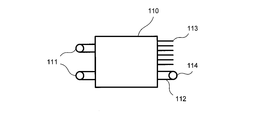
- FIG. 2B shows the configuration of the power module 110.
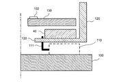
- 3A shows a cross-sectional view of power converter 50 taken along the line IIIA-IIIA in FIG. 2A.
- 3B shows a cross-sectional view of the power converter 50 taken along the line IIIB-IIIB in FIG. 2A.
- the power conversion device 50 has a cylindrical shape and has a cooler 100 having a flat top portion on the upper surface thereof, and the respective parts are stacked on the top side of the cooler 100.
- the power conversion device 50 is provided, for example, on one end side in the axial direction of a driving motor M having a cylindrical shape.
- the outer shape of the cooler 100 and other configurations does not necessarily have to be circular, and may be polygonal.
- a plurality of power modules 110 are placed on the top of the cooler 100 at predetermined intervals in the circumferential direction along the circular shape of the top.
- the power module 110 is a module in which a power semiconductor 31, a diode 32, and the like are enclosed in the same package. In the present embodiment, ten power modules 110 are placed on the top of the cooler 100.
- the power module 110 includes a PN terminal 111 that receives supply of high-voltage DC power, an AC terminal 112 that outputs AC high-frequency power, and a plurality of control signal terminals 113 that are connected to a control board 150 described later.
- the power module 110 is placed on the top of the cooler 100 with the PN terminal 111 facing the inner periphery and the AC terminal 112 and the control signal terminal 113 facing the outer periphery.
- the AC terminal 112 is provided with an AC bus bar 114 extending toward the outer periphery of the cooler 100 and extending upward of the cooler 100.
- the AC bus bar 114 is electrically connected to the drive motor M.
- a DC bus bar 120 that supplies DC power to the power module 110 is disposed on the upper side of the power module 110.
- the DC bus bar 120 has an annular shape along the shape of the top of the cooler 100.
- the DC bus bar 120 has a positive electrode and a negative electrode. The positive electrode and the negative electrode are connected to PN terminals provided in the power module 110, respectively.
- a pair of pins 121 and 122 communicating with the positive electrode and the negative electrode are extended upward at two locations on the outer side in the circumferential direction of the DC bus bar 120.
- a plurality of smoothing capacitors 40 are placed on the upper surface of the DC bus bar 120 at predetermined intervals in the circumferential direction. Smoothing capacitor 40 is electrically connected to the positive electrode and the negative electrode of DC bus bar 120, respectively.
- a first substrate 130 having an annular shape substantially the same shape as the DC bus bar 120 is disposed further above the DC bus bar 120.
- weak current components such as a current sensor 131 and a pad 132 are mounted to constitute a weak current substrate.
- the first substrate 130 is formed with notches 135 and 136 for avoiding contact with the pins 121 and 122 extending above the DC bus bar 120.
- the DC bus bar 120 and the first substrate 130 have a circular hollow portion 120a formed on the inner peripheral side.
- the current sensor 131 detects the output current from the AC bus bar 114 of the power module 110.
- the current sensor 131 is configured to include, for example, a Hall element, and detects the current of the AC bus bar 114 by a change in magnetic flux of the AC bus bar 114 extending upward.
- the pad 132 is provided in an annular shape on the inner peripheral side of the first substrate 130, and functions as a connection portion to which a connection wiring that is electrically connected to a drive motor M (not shown) is connected.
- the pad 132 is electrically connected to, for example, a controller provided in the drive motor M by a cable, and values such as electric power, rotation speed, and temperature input to the drive motor M are input.
- a control board 150 (second board) is provided on each outer peripheral side of the plurality of power modules 110 placed on the cooler 100.
- the control board 150 includes the control circuit 10 and controls the operation of the power semiconductor 31 of the power module 110.
- the control board 150 is provided in the vertical direction from the top of the cooler 100.
- the lower side of the control board 150 is connected to the control signal terminal 113 of the power module 110, and the upper side of the control board 150 is connected to the signal terminal 133 of the first board 130. Therefore, the lower side of the control board 150 is supported by the control signal terminal 113 of the power module 110, and the upper side is supported by the signal terminal 133 of the first board 130.
- the power module 110 is mounted on the upper surface of the cooler 100 serving as a base.
- a DC bus bar 120 and a first substrate 130 as a weak electrical substrate are sequentially stacked.
- the control board 150 is fixed to and electrically connected to the power module 110 and the first board 130, respectively.
- control board 150 is fixed at the upper and lower portions of the power module 110 and the first board 130, so that the durability of the control board 150 with respect to external stresses such as vibrations and shocks is increased. Reliability can be improved.
- control board 150 is arranged so as to be perpendicular to the installation direction of the power module 110 including the power semiconductor 31, it is possible to suppress the influence of noise and heat of the power module 110.
- the first board 130 as the weak electric board on which the weak electric equipment such as the current sensor 131 and the pad 132 is mounted is separated from the power module 110 and the control board 150, noise and heat affect the low electric equipment. Can be suppressed.
- the smoothing capacitor 40 mounted on the DC bus bar 120 is disposed between the power module 110 and the first substrate 130 as the weak electric substrate, it is possible to suppress noise and heat from affecting the low electric device.
- a pad 132 to which a signal line for transmitting and receiving signals to and from the driving motor M is connected is provided on the inner peripheral side of the first substrate 130, and an AC bus bar from which the high frequency high voltage of the power module 110 is output. 114 is provided on the outer peripheral side of the first substrate 130.
- FIG. 4 shows a top view of the power converter 50.
- FIG. 5A shows a VA-VA cross-sectional view of the power conversion device 50 in FIG.
- FIG. 5B shows a VB-VB cross-sectional view of the power converter 50 in FIG.
- the basic configuration of the second embodiment is the same as that of the first embodiment.
- the same components as those of the first embodiment are denoted by the same reference numerals, and the description thereof is omitted.
- control board 150 on which the control circuit 10 is mounted is formed of a flexible board and arranged in a cylindrical shape on the outer peripheral side of the power module 110 and the first board 130.
- the control board 150 can be formed into an integral shape, and further, the power module 110 and the first board 130 are respectively fixed at two locations above and below, so that the vibration The durability reliability of the control board 150 can be improved against external stress such as shock and impact.
- FIG. 6, FIG. 7A and FIG. 7B are explanatory diagrams of the power conversion device 50 according to the third embodiment of the present invention.
- FIG. 6 shows a top view of the power converter 50.
- 7A is a cross-sectional view of the power conversion device 50 taken along the line VIIA-VIIA in FIG. 7B is a cross-sectional view of the power converter 50 taken along the line VIIB-VIIB in FIG.
- the basic configuration of the third embodiment is the same as that of the first embodiment.
- the same components as those of the first or second embodiment are denoted by the same reference numerals, and the description thereof is omitted.
- the current sensor 131 that detects the current of the AC bus bar 114 is mounted on the control board 150 on which the control circuit 10 is mounted.
- the AC bus bar 114 and the current sensor 131 can be brought closer to each other by mounting the current sensor 131 that detects the current of the AC bus bar 114 on the control board 150 side. It is possible to prevent the detected value from varying due to the influence of the above.
- the AC bus bar 114 and the first substrate 130 which is a weak electric substrate can be separated from each other, the first substrate 130 is hardly affected by the high frequency high voltage of the AC bus bar 114.
- FIG. 8, FIG. 9A and FIG. 9B are explanatory diagrams of the power conversion device 50 according to the fourth embodiment of the present invention.
- FIG. 8 shows a top view of the power converter 50.
- FIG. 9A shows a cross-sectional view of the power converter 50 taken along the line IXA-IXA in FIG.
- FIG. 9B is a sectional view of the power conversion device 50 taken along the line IXB-IXB in FIG.
- the basic configuration of the fourth embodiment is the same as that of the first embodiment.
- the same components as those of the first to third embodiments are denoted by the same reference numerals, and the description thereof is omitted.
- the third substrate in addition to the substrate 130 on which the current sensor 131 and the pad 132 are mounted, the third substrate further includes a signal wiring that connects signals from the current sensor 131 and the pad 132 to the control substrate 150. 160.
- the first substrate 130 has the current sensor 131 and the pad 132 mounted thereon, the signal lines are wired to the third substrate 160, and the signal terminals 161 connected to the third substrate 160. Was configured to be connected to the control board 150.
- the first substrate 130 which is a weak electrical substrate
- the control substrate which is a strong electrical substrate
- the third substrate 160 can be separated through the third substrate 160 in this way, so that noise caused by the control substrate 150 can be reduced. Can be suppressed from affecting the weak electrical equipment.
- the third substrate 160 is interposed between the power module 110 and the first substrate 130 in addition to the smoothing capacitor 40, noise and heat of the power module 110 are weakly charged by the first substrate 130. It can suppress affecting the equipment.
- FIG. 11A and FIG. 11B are explanatory diagrams of a power conversion device 50 according to the fifth embodiment of the present invention.
- FIG. 10 shows a top view of the power converter 50.
- FIG. 11A is a cross-sectional view of the power conversion device 50 taken along the line XIA-XIA in FIG.
- FIG. 11B shows a cross-sectional view of the power converter 50 taken along the line XIB-XIB in FIG.
- the basic configuration of the fifth embodiment is the same as that of the first embodiment.
- the same components as those of the first to fourth embodiments are denoted by the same reference numerals, and the description thereof is omitted.
- the fifth embodiment is a modification of the above-described fourth embodiment, in which a current sensor 131 is mounted on the first substrate 130 and a pad 132 is mounted on the third substrate 160.
- the current sensor 131 that is particularly susceptible to noise and heat can be separated from the control board 150. Further, since the third substrate 160 is interposed between the power module 110 and the first substrate 130 in addition to the smoothing capacitor 40, the noise and heat of the power module 110 can cause the current of the first substrate 130 to flow. The influence on the sensor 131 can be suppressed.
- the connectivity with the driving motor M can be improved.
- FIG. 12, FIG. 13A and FIG. 13B are explanatory diagrams of a power conversion apparatus 50 according to the sixth embodiment of the present invention.
- FIG. 12 shows a top view of the power converter 50.
- 13A is a cross-sectional view of the power conversion device 50 taken along the line XIIIA-XIIIA in FIG.
- FIG. 13B shows a cross-sectional view of power converter 50 taken along line XIIIB-XIIIB in FIG.
- the basic configuration of the sixth embodiment is the same as that of the first embodiment, and the same reference numerals are given to the same components as those of the first to fifth embodiments, and the description thereof is omitted.
- the sixth embodiment is a modification of the above-described fourth embodiment and fifth embodiment, in which a current sensor 131 is mounted on a first substrate 130, and the first substrate 130 and the third substrate. 160 is mounted with a first pad 132A and a second pad 132B, respectively.
- the degree of freedom in handling signal lines is improved, and the connectivity with the driving motor M can be improved.
- FIG. 15A and FIG. 15B are explanatory diagrams of a power conversion device 50 according to a seventh embodiment of the present invention.
- FIG. 14 is a top view of the power conversion device 50.
- 15A is a cross-sectional view of the power conversion device 50 taken along the line XVA-XVA in FIG.
- FIG. 15B shows an XVB-XVB cross-sectional view of the power converter 50 in FIG.
- the basic configuration of the seventh embodiment is the same as that of the first embodiment.
- the same components as those of the first to sixth embodiments are denoted by the same reference numerals, and the description thereof is omitted.
- the power module 110 placed on the upper surface of the cooler 100 is connected to the AC bus bar 114 and the control signal terminal 113 on the inner peripheral side, and the PN terminal. It arrange
- Ten power modules 110 are placed at predetermined intervals in the circumferential direction along the circular shape at the top of the cooler 100.
- control board 150 was arranged on the inner circumference side of the circumference where the power module 110 is arranged.
- the DC bus bar 120 is disposed on the upper side of the power module 110, and pins 121 and 122 are extended upward at two locations on the inner peripheral side of the annular DC bus bar 120.
- a first substrate 130 is disposed above the DC bus bar 120, and notches 135 for avoiding contact with the pins 121 and 122 of the DC bus bar 120 at two locations on the inner peripheral side of the first substrate 130. 136 are formed.
- the pads 132 provided on the first substrate 130 are provided in an annular shape on the outer peripheral side of the first substrate 130.
- the AC bus bar 114 extending upward from the power module 110 extends upward from the DC bus bar 120 and the circular hollow portion 120a on the inner peripheral side of the first substrate 130.
- the pins 121 and 122 of the DC bus bar 120 also extend upward from the DC bus bar 120 and the circular hollow portion 120 a on the inner peripheral side of the first substrate 130.
- the control board 150 is fixed to the control signal terminal 113 of the power module 110 on the lower side and the signal terminal 133 of the first board 130 on the upper side along the hollow portion 120a.
- the AC bus bar 114 and the DC bus bar 120 are extended from the inner peripheral side to the upper side, and the pad 132 for connecting the signal line to the driving motor M is provided on the outer peripheral side. It was configured as follows. With such a configuration, the degree of freedom in handling the signal lines connected to the DC bus bar 120, the AC bus bar 114, and the pad 132 is improved, and the connectivity with the drive motor M can be improved.
- FIG. 17A and FIG. 17B are explanatory diagrams of the power conversion device 50 according to the eighth embodiment of the present invention.
- FIG. 16 shows a top view of the power converter 50.
- FIG. 17A shows a cross-sectional view of power converter 50 taken along line XVIIA-XVIIA in FIG.
- FIG. 17B is a cross-sectional view of power converter 50 taken along XVIIB-XVIIB in FIG.
- the basic configuration of the eighth embodiment is the same as that of the first embodiment, and the same reference numerals are given to the same components as those of the first to seventh embodiments, and the description thereof is omitted.
- the eighth embodiment is a modification of the above-described seventh embodiment, in which the control board 150 is arranged on the inner circumference side of the circumference where the power module 110 is arranged, and the AC bus bar 114 is arranged on the inner circumference side. It was comprised so that it might extend upward from.
- the signals from the current sensor 131 and the pad 132 are further controlled as in the fourth embodiment.
- a third substrate 160 connected to the substrate 150 was provided.
- the control board 150 is connected to the control signal terminal 113 of the power module 110 on the lower side and the third board 160 on the upper side along the circular hollow portion 120a on the inner peripheral side of the DC bus bar 120 and the first board 130. , Each fixed.
- the pins 121 and 122 of the DC bus bar 120 and the notches 134 and 135 of the first substrate 130 are provided on the outer peripheral side, but are provided on the inner peripheral side as in the seventh embodiment described above. May be.
- FIG. 18, FIG. 19A and FIG. 19B are explanatory diagrams of the power conversion device 50 according to the ninth embodiment of the present invention.
- FIG. 18 is a top view of the power conversion device 50.
- FIG. 19A is a cross-sectional view of the power converter 50 taken along the line XIXA-XIXA in FIG.
- FIG. 19B is a cross-sectional view of the power converter 50 taken along the line XIXB-XIXB in FIG.
- the basic configuration of the ninth embodiment is the same as that of the first embodiment.
- the same components as those of the first to eighth embodiments are denoted by the same reference numerals, and the description thereof is omitted.
- the ninth embodiment is a modification of the seventh embodiment, and the power modules 110 placed on the upper surface of the cooler 100 are arranged so that their directions are staggered. That is, the power module 110 in which the AC bus bar 114 and the control signal terminal 113 are on the inner peripheral side and the power module 110 in which the AC bus bar 114 and the control signal terminal 113 are on the outer peripheral side are alternately arranged.
- the pins 121 and 122 of the DC bus bar 120 and the notches 134 and 135 of the first substrate 130 are provided on the outer peripheral side.
- the inner peripheral side is provided. You may prepare for.
- the AC bus bar 114 is thus extended upward from the inner peripheral side in this way.
- the degree of freedom in handling the signal lines connected to the DC bus bar 120, the AC bus bar 114, and the pad 132 is improved, and the connectivity with the drive motor M can be improved.
- the power conversion device 50 including the power semiconductor 31 and the diode 32 and configuring the inverter has been described.
- the present invention is not limited to this configuration.
- the above-described embodiment can be similarly applied to a semiconductor device having a semiconductor element and a control substrate and a weak electric substrate related to the operation of the semiconductor element.
- control board 150 may be formed of a flexible board having flexibility.
Landscapes
- Engineering & Computer Science (AREA)
- Power Engineering (AREA)
- Microelectronics & Electronic Packaging (AREA)
- Inverter Devices (AREA)
- Physics & Mathematics (AREA)
- Thermal Sciences (AREA)
Priority Applications (3)
| Application Number | Priority Date | Filing Date | Title |
|---|---|---|---|
| US14/382,671 US20150029672A1 (en) | 2012-03-07 | 2013-02-27 | Power conversion apparatus |
| EP13757512.2A EP2824821A4 (en) | 2012-03-07 | 2013-02-27 | POWER CONVERSION |
| CN201380012461.4A CN104205600A (zh) | 2012-03-07 | 2013-02-27 | 电力转换装置 |
Applications Claiming Priority (2)
| Application Number | Priority Date | Filing Date | Title |
|---|---|---|---|
| JP2012050627A JP2013187998A (ja) | 2012-03-07 | 2012-03-07 | 電力変換装置 |
| JP2012-050627 | 2012-03-07 |
Publications (1)
| Publication Number | Publication Date |
|---|---|
| WO2013133104A1 true WO2013133104A1 (ja) | 2013-09-12 |
Family
ID=49116586
Family Applications (1)
| Application Number | Title | Priority Date | Filing Date |
|---|---|---|---|
| PCT/JP2013/055144 Ceased WO2013133104A1 (ja) | 2012-03-07 | 2013-02-27 | 電力変換装置 |
Country Status (5)
| Country | Link |
|---|---|
| US (1) | US20150029672A1 (https=) |
| EP (1) | EP2824821A4 (https=) |
| JP (1) | JP2013187998A (https=) |
| CN (1) | CN104205600A (https=) |
| WO (1) | WO2013133104A1 (https=) |
Families Citing this family (13)
| Publication number | Priority date | Publication date | Assignee | Title |
|---|---|---|---|---|
| JP5888010B2 (ja) * | 2012-03-08 | 2016-03-16 | 日産自動車株式会社 | インバータモジュール |
| EP2790217A1 (de) * | 2013-04-09 | 2014-10-15 | ABB Technology AG | Leistungshalbleitermodul |
| JP2015050257A (ja) * | 2013-08-30 | 2015-03-16 | 株式会社東芝 | 車両用電力変換装置及び鉄道車両 |
| JP6383614B2 (ja) * | 2014-09-08 | 2018-08-29 | 京セラ株式会社 | コンデンサモジュール及びパワーユニット |
| CN107112317B (zh) | 2014-12-24 | 2019-07-05 | 日本精工株式会社 | 功率半导体模块以及使用其的电动助力转向装置 |
| JP6455154B2 (ja) * | 2015-01-08 | 2019-01-23 | 株式会社デンソー | 車両用電子機器 |
| DE102015113503A1 (de) * | 2015-08-14 | 2017-02-16 | Schweizer Electronic Ag | Elektronisches Schaltelement und modular aufgebauter Stromrichter |
| DE102015219867A1 (de) * | 2015-10-13 | 2017-04-13 | Lenze Drives Gmbh | Platine, B-Lagerschild, Motorbausatz und Elektromotor |
| JP6098705B1 (ja) * | 2015-12-28 | 2017-03-22 | ダイキン工業株式会社 | インバータ |
| WO2017149801A1 (ja) * | 2016-03-02 | 2017-09-08 | 三菱電機株式会社 | 電力変換装置 |
| JP6143980B1 (ja) * | 2016-03-02 | 2017-06-07 | 三菱電機株式会社 | 電力変換装置 |
| JP7239380B2 (ja) * | 2019-04-16 | 2023-03-14 | 株式会社日立製作所 | 電力変換装置 |
| CN114846600A (zh) * | 2019-12-28 | 2022-08-02 | 丹佛斯硅动力有限责任公司 | 具有改进的电气特性和热特性的功率模块 |
Citations (4)
| Publication number | Priority date | Publication date | Assignee | Title |
|---|---|---|---|---|
| JP2009165327A (ja) * | 2008-01-10 | 2009-07-23 | Mitsubishi Electric Corp | インバータ装置及びその製造方法 |
| JP2009212311A (ja) * | 2008-03-04 | 2009-09-17 | Toyota Industries Corp | 電子機器 |
| JP2010124691A (ja) * | 2010-03-08 | 2010-06-03 | Hitachi Automotive Systems Ltd | 電力変換装置 |
| JP2011078309A (ja) * | 2006-01-16 | 2011-04-14 | Mitsubishi Electric Corp | 電動機の駆動回路及び空気調和機の室外機 |
Family Cites Families (9)
| Publication number | Priority date | Publication date | Assignee | Title |
|---|---|---|---|---|
| US5907475A (en) * | 1996-04-16 | 1999-05-25 | Allen-Bradley Company, Llc | Circuit board system having a mounted board and a plurality of mounting boards |
| JP3949368B2 (ja) * | 2000-10-17 | 2007-07-25 | 三菱電機株式会社 | 車両用交流発電機 |
| JP4434181B2 (ja) * | 2006-07-21 | 2010-03-17 | 株式会社日立製作所 | 電力変換装置 |
| US8008805B2 (en) * | 2006-12-07 | 2011-08-30 | Nissan Motor Co., Ltd. | Power conversion apparatus and motor drive system |
| JP4771972B2 (ja) * | 2007-02-13 | 2011-09-14 | トヨタ自動車株式会社 | 電力変換装置 |
| JP4567029B2 (ja) * | 2007-06-22 | 2010-10-20 | 日立オートモティブシステムズ株式会社 | 電力変換装置 |
| JP5260347B2 (ja) * | 2009-02-06 | 2013-08-14 | 日立オートモティブシステムズ株式会社 | 電力変換装置 |
| DE102010017522A1 (de) * | 2009-06-24 | 2011-02-03 | ASMO Co., Ltd., Kosai-city | Antriebsvorrichtung und Halbleitermodul |
| WO2012093476A1 (ja) * | 2011-01-06 | 2012-07-12 | 三菱電機株式会社 | 回転電機 |
-
2012
- 2012-03-07 JP JP2012050627A patent/JP2013187998A/ja not_active Withdrawn
-
2013
- 2013-02-27 CN CN201380012461.4A patent/CN104205600A/zh active Pending
- 2013-02-27 EP EP13757512.2A patent/EP2824821A4/en not_active Withdrawn
- 2013-02-27 US US14/382,671 patent/US20150029672A1/en not_active Abandoned
- 2013-02-27 WO PCT/JP2013/055144 patent/WO2013133104A1/ja not_active Ceased
Patent Citations (5)
| Publication number | Priority date | Publication date | Assignee | Title |
|---|---|---|---|---|
| JP2011078309A (ja) * | 2006-01-16 | 2011-04-14 | Mitsubishi Electric Corp | 電動機の駆動回路及び空気調和機の室外機 |
| JP2009165327A (ja) * | 2008-01-10 | 2009-07-23 | Mitsubishi Electric Corp | インバータ装置及びその製造方法 |
| JP2009212311A (ja) * | 2008-03-04 | 2009-09-17 | Toyota Industries Corp | 電子機器 |
| JP4609504B2 (ja) | 2008-03-04 | 2011-01-12 | 株式会社豊田自動織機 | 電子機器 |
| JP2010124691A (ja) * | 2010-03-08 | 2010-06-03 | Hitachi Automotive Systems Ltd | 電力変換装置 |
Non-Patent Citations (1)
| Title |
|---|
| See also references of EP2824821A4 |
Also Published As
| Publication number | Publication date |
|---|---|
| CN104205600A (zh) | 2014-12-10 |
| EP2824821A4 (en) | 2015-10-21 |
| EP2824821A1 (en) | 2015-01-14 |
| US20150029672A1 (en) | 2015-01-29 |
| JP2013187998A (ja) | 2013-09-19 |
Similar Documents
| Publication | Publication Date | Title |
|---|---|---|
| WO2013133104A1 (ja) | 電力変換装置 | |
| EP3220521B1 (en) | Control unit and electric power steering device using same | |
| US10759467B2 (en) | Integrated electric power steering apparatus | |
| US9425707B2 (en) | Inverter device capable of appropriately fixing a power module having a switching element and a smoothing capacitor in a limited region | |
| JP4597202B2 (ja) | 電力変換装置 | |
| CN107343387B (zh) | 电力转换装置 | |
| US9117789B2 (en) | Semiconductor device | |
| WO2016132474A1 (ja) | 一体型電動パワーステアリング装置 | |
| JP2009130967A (ja) | モータの制御装置 | |
| JP6176135B2 (ja) | 電力変換装置 | |
| JP2013017310A (ja) | 電力変換装置 | |
| JP2012100457A (ja) | 電力変換装置 | |
| JP5888014B2 (ja) | 電力変換装置 | |
| JPWO2016117403A1 (ja) | 電力変換装置 | |
| JP2011135725A (ja) | 電力変換装置 | |
| US20140167554A1 (en) | Squirrel Cage Rotor and Rotary Electric Machine | |
| RU2330371C1 (ru) | Тяговый мехатронный модуль | |
| JP2013099211A (ja) | インバータ回路の制御装置 | |
| JP7334750B2 (ja) | 電気機器 | |
| JP2005278296A (ja) | コンデンサ装置およびそれを備えた電源システム | |
| JP2020162226A (ja) | 電力変換ユニット | |
| JP5704054B2 (ja) | 電力変換装置 | |
| WO2022054476A1 (ja) | 電力変換装置 | |
| JP6485283B2 (ja) | 電力変換装置 | |
| WO2016186087A1 (ja) | コンデンサモジュール |
Legal Events
| Date | Code | Title | Description |
|---|---|---|---|
| 121 | Ep: the epo has been informed by wipo that ep was designated in this application |
Ref document number: 13757512 Country of ref document: EP Kind code of ref document: A1 |
|
| NENP | Non-entry into the national phase |
Ref country code: DE |
|
| WWE | Wipo information: entry into national phase |
Ref document number: 14382671 Country of ref document: US |
|
| WWE | Wipo information: entry into national phase |
Ref document number: 2013757512 Country of ref document: EP |