WO2013129308A1 - 放射線画像撮影用吸収型グリッド及びその製造方法、並びに放射線画像撮影システム - Google Patents
放射線画像撮影用吸収型グリッド及びその製造方法、並びに放射線画像撮影システム Download PDFInfo
- Publication number
- WO2013129308A1 WO2013129308A1 PCT/JP2013/054750 JP2013054750W WO2013129308A1 WO 2013129308 A1 WO2013129308 A1 WO 2013129308A1 JP 2013054750 W JP2013054750 W JP 2013054750W WO 2013129308 A1 WO2013129308 A1 WO 2013129308A1
- Authority
- WO
- WIPO (PCT)
- Prior art keywords
- thin film
- grid
- radiation
- support substrate
- metal layer
- Prior art date
- Legal status (The legal status is an assumption and is not a legal conclusion. Google has not performed a legal analysis and makes no representation as to the accuracy of the status listed.)
- Ceased
Links
Images





Classifications
-
- G—PHYSICS
- G21—NUCLEAR PHYSICS; NUCLEAR ENGINEERING
- G21K—HANDLING OF PARTICLES OR IONISING RADIATION NOT OTHERWISE PROVIDED FOR; IRRADIATION DEVICES; GAMMA RAY OR X-RAY MICROSCOPES
- G21K1/00—Arrangements for handling particles or ionising radiation, e.g. focusing or moderating
- G21K1/06—Arrangements for handling particles or ionising radiation, e.g. focusing or moderating using diffraction, refraction or reflection, e.g. monochromators
-
- A—HUMAN NECESSITIES
- A61—MEDICAL OR VETERINARY SCIENCE; HYGIENE
- A61B—DIAGNOSIS; SURGERY; IDENTIFICATION
- A61B6/00—Apparatus or devices for radiation diagnosis; Apparatus or devices for radiation diagnosis combined with radiation therapy equipment
- A61B6/40—Arrangements for generating radiation specially adapted for radiation diagnosis
- A61B6/4035—Arrangements for generating radiation specially adapted for radiation diagnosis the source being combined with a filter or grating
-
- A—HUMAN NECESSITIES
- A61—MEDICAL OR VETERINARY SCIENCE; HYGIENE
- A61B—DIAGNOSIS; SURGERY; IDENTIFICATION
- A61B6/00—Apparatus or devices for radiation diagnosis; Apparatus or devices for radiation diagnosis combined with radiation therapy equipment
- A61B6/42—Arrangements for detecting radiation specially adapted for radiation diagnosis
- A61B6/4291—Arrangements for detecting radiation specially adapted for radiation diagnosis the detector being combined with a grid or grating
-
- G—PHYSICS
- G21—NUCLEAR PHYSICS; NUCLEAR ENGINEERING
- G21K—HANDLING OF PARTICLES OR IONISING RADIATION NOT OTHERWISE PROVIDED FOR; IRRADIATION DEVICES; GAMMA RAY OR X-RAY MICROSCOPES
- G21K2207/00—Particular details of imaging devices or methods using ionizing electromagnetic radiation such as X-rays or gamma rays
- G21K2207/005—Methods and devices obtaining contrast from non-absorbing interaction of the radiation with matter, e.g. phase contrast
Definitions
- the present invention relates to an absorption grid for radiographic imaging, a manufacturing method thereof, and a radiographic imaging system using the grid.
- X-ray When radiation such as X-rays (hereinafter, X-ray is taken as an example) is irradiated on a subject such as a human body, the intensity and phase change due to the interaction with the subject.
- X-ray imaging apparatuses that are widely used image the transmitted X-ray intensity. For example, since bones and the like have low X-ray transmittance, and tissues such as muscles have high X-ray transmittance, when the distribution of transmitted X-ray intensity is imaged, it is possible to identify tissues having different X-ray transmittances. it can.
- an X-ray intensity image obtained by imaging the intensity of transmitted X-rays (hereinafter referred to as an X-ray intensity image)
- a tissue having a high X-ray transmittance is typically black and a tissue having a low X-ray transmittance is white.
- tissues having different X-ray transmittances can be identified.
- tissues having similar X-ray transmittances are adjacent to each other, it is not easy to identify them.
- soft tissues such as cartilage have a high X-ray transmittance
- tissues and body fluids adjacent to the periphery have a high X-ray transmittance, so that the soft tissue is difficult to be reflected in an X-ray intensity image.
- lesions also occur in tissues that are difficult to see in an X-ray intensity image, it is desired that these can be identified by X-ray imaging.
- phase contrast image an X-ray image that can identify a soft tissue having a high X-ray transmittance is obtained by imaging a subject based on a phase change of transmitted X-rays (phase imaging).
- an X-ray imaging system that performs phase imaging, in order to obtain information on a phase change of transmitted X-rays, at least two grids are arranged between an X-ray source and an X-ray detector to image a subject. . Specifically, the first grid and the second grid are arranged oppositely between the X-ray source and the X-ray detector, and the X-rays emitted from the X-ray source are passed through the first grid, thereby An X-ray image having a self-image of one grid is generated. For example, the Talbot effect is used to generate the X-ray image.
- X-ray detection is performed on the X-ray image that has passed through the first grid and the second grid while the position of the second grid is gradually changed in the in-plane direction with respect to the X-ray image generated by the first grid.
- a phase contrast image can be generated based on a plurality of images obtained by photographing.
- This X-ray image capturing method is called a fringe scanning method.
- a source grid may be provided between the X-ray source and the first grid to disperse the X-ray focal point and improve the contrast of the X-ray image.
- the first grid either an absorption grid that partially absorbs X-rays or a phase grid that partially modulates and transmits the X-ray phase can be used.
- an absorption grid for the second grid and the source grid it is necessary to use an absorption grid for the second grid and the source grid.
- the absorption grid needs to have a high aspect ratio.
- the absorption grid is formed by periodically forming a groove having a high aspect ratio on the surface of a substrate such as silicon and embedding a metal material (X-ray absorber) such as gold (Au) in the groove.
- a metal material such as gold (Au)
- electroplating is used as a method of almost uniformly embedding a metal material in a groove having a high aspect ratio. In order to perform this electroplating, it is necessary to provide a sheath electrode at the bottom of the groove. .
- Diffusion bonding is a method of bonding by utilizing the diffusion of atoms between contact surfaces by applying pressure and heating to such an extent that plastic deformation does not occur on the base material substrate. For this reason, the state of bonding by diffusion bonding is greatly influenced by the flatness and cleanliness of the surfaces to be bonded. That is, if there are irregularities or dust on the joint surface, an unjoined portion (void or the like) is generated, and joint failure or separation after joining is likely to occur. For this reason, it is desirable to employ a bonding method that is less likely to cause bonding defects than diffusion bonding in forming the sheath electrode.
- Anodic bonding is a bonding method in which, for example, a semiconductor such as silicon and glass (or metal and glass) are bonded by applying a voltage while heating. For this reason, a metal thin film is formed on one surface of two substrates, these are anodically bonded, a plurality of grooves having a high aspect ratio are formed on one substrate, and the metal thin film is exposed on the bottom thereof. If electroplating is performed using a metal thin film as a seed electrode, an absorption grid can be manufactured. However, if there are irregularities or dust on the bonding surface, unbonded portions (voids, etc.) are generated, and bonding failure and peeling after bonding are likely to occur, as in the case of using diffusion bonding.
- An object of the present invention is to provide an absorption grid for radiographic imaging and a method for manufacturing the same, which prevent a bonding failure or separation after bonding from occurring at the interface between two substrates. It is another object of the present invention to provide a radiation imaging system using this radiation image capturing absorption grid.
- the absorption grid for radiographic imaging of the present invention includes a grid layer, a support substrate, and a metal layer.
- the grid layer has a structure in which radiation absorbing parts that absorb radiation and radiation transmitting parts that transmit radiation are alternately arranged in a direction perpendicular to the incident direction of the radiation.
- the support substrate has an ion conductive material at least on the surface on the grid layer side, and supports the grid layer.
- the metal layer is provided between the grid layer and the support substrate, is in close contact with the radiation transmitting portion of the grid layer by film formation, and is bonded to the support substrate by anodic bonding. Furthermore, the metal layer includes a first thin film and a second thin film or a third thin film.
- the first thin film is a metal thin film that functions as a sheath electrode when the radiation absorbing portion is formed by electroplating.
- the second thin film is a metal thin film provided between the first thin film and the grid layer, which has better adhesion to the radiation transmitting portion than the first thin film.
- the third thin film is a metal thin film provided between the first thin film and the support substrate, which has better bondability to the support substrate than the first thin film in the anodic bonding.
- the metal layer preferably has a three-layer structure of a second thin film, a first thin film, and a third thin film.
- the first thin film is in direct contact with the radiation absorbing portion without passing through the second thin film.
- an insulating film is formed on the surface of the radiation transmitting portion.
- the second thin film is titanium, chromium, nickel, or an alloy containing any of these.
- the first thin film is gold, platinum, iridium, palladium, rhodium, or an alloy containing any of these.
- the third thin film is aluminum, nickel, molybdenum, tungsten, or an alloy containing any of these.
- the thermal expansion coefficients of the first thin film, the second thin film, and the third thin film are greater than or equal to the thermal expansion coefficient of the support substrate and the radiation transmitting portion. It is preferable that it is below a thermal expansion coefficient.
- the thermal expansion coefficients of the first thin film, the second thin film, and the third thin film are equal to or lower than the thermal expansion coefficient of the support substrate and of the radiation transmitting portion. It is preferable that the coefficient of thermal expansion is greater than the thermal expansion coefficient, and the coefficient of thermal expansion is increased stepwise in the order of the radiation transmitting portion, the second thin film, the first thin film, the third thin film, and the support substrate.
- the support substrate is preferably an ion conductive substrate.
- the supporting substrate is composed of a substrate formed of the same material as the radiation transmitting portion and an ion conductive thin film provided on the substrate, and is preferably bonded to the metal layer by the ion conductive thin film.
- the manufacturing method of the absorption grid for radiographic imaging of the present invention includes a metal layer forming step, a joining step, an etching step, and an electroplating step.
- the metal layer forming step on one surface of the etching substrate made of a material of a radiation transmitting portion that transmits radiation, in addition to the first thin film that becomes a sheath electrode in the electroplating step, the first thin film is formed or formed. Thereafter, at least one of the second thin film and the third thin film is formed, and a metal layer having at least two types of metal thin films is formed.
- the second thin film has better adhesion to the etching substrate than the seed electrode, and is formed between the first thin film and the etching substrate.
- the third thin film has better bondability with the support substrate than the sheath electrode, and is formed on the first thin film.
- the bonding step the support substrate is brought into contact with the metal layer to perform anodic bonding, thereby forming a bonded body of the etching substrate on which the metal layer is formed and the support substrate.
- the etching step the etching substrate of the joined body is etched into a predetermined pattern, a groove serving as a radiation absorbing portion for absorbing radiation and a radiation transmitting portion are formed, and the metal layer is exposed at the bottom of the groove.
- the metal layer exposed in the groove is used as a seed electrode, and a radiation absorbing material that absorbs radiation is embedded in the groove by electroplating.
- the second thin film, the first thin film, and the third thin film are formed in this order on the etching substrate to form the metal layer composed of three types of metal thin films.
- the metal layer forming step it is preferable to form a plurality of metal thin films without breaking the vacuum using the same film forming apparatus.
- the radiographic imaging system of the present invention is a radiographic imaging system that captures radiation irradiated from a radiation source through an absorption grid to generate a phase contrast image.
- the absorption grid includes a grid layer and a support substrate.
- the grid layer has a structure in which radiation absorbing parts that absorb radiation and radiation transmitting parts that transmit radiation are alternately arranged in a direction perpendicular to the incident direction of the radiation.
- the support substrate has an ion conductive material at least on the surface on the grid layer side, and supports the grid layer.
- the metal layer is provided between the grid layer and the support substrate, is in close contact with the radiation transmitting portion of the grid layer by film formation, and is bonded to the support substrate by anodic bonding.
- the metal layer includes a first thin film and a second thin film or a third thin film.
- the first thin film is a metal thin film that functions as a sheath electrode when the radiation absorbing portion is formed by electroplating.
- the second thin film is a metal thin film provided between the first thin film and the grid layer, which has better adhesion to the radiation transmitting portion than the first thin film.
- the third thin film is a metal thin film provided between the first thin film and the support substrate, which has better bondability to the support substrate than the first thin film in the anodic bonding.
- the absorption grid for radiographic imaging of the present invention is a metal thin film having better adhesion to the radiation transmitting portion than the sheath electrode on at least one of the front and rear sides of the sheath electrode, or a junction with the support substrate rather than the sheath electrode in anodic bonding. Since any of the metal thin films having good properties is included, problems such as peeling due to poor bonding at the boundary surface where the sheath electrode is formed are unlikely to occur.
- the X-ray imaging system 10 includes an X-ray source 11, a source grid 12, a first grid 13, a second grid 14, and an X-ray along the Z direction that is an X-ray irradiation direction.
- An image detector 15 is provided.
- the X-ray source 11 has a rotating anode type X-ray tube (not shown) and a collimator (not shown) for limiting the X-ray irradiation field, and emits X-rays to the subject H.
- the source grid 12 and the second grid 14 are absorption grids that partially absorb X-rays, and linear X-ray absorption parts and X-ray transmission parts are alternately arranged.
- the first grid 13 is a phase type grid that generates a predetermined phase difference (for example, ⁇ or ⁇ / 2) by the uneven structure of the substrate.
- Each of the grids 12 to 14 is disposed so as to face the X-ray source 11 in the Z direction, and in each case, a grid line is provided along the X direction.
- the distance between the first grid 13 and the second grid 14 is set to a Talbot distance, for example.
- the Talbot distance is a distance at which X-rays that have passed through the first grid 13 generate a self-image of the first grid 13 due to the Talbot effect.
- the X-ray image detector 15 is a flat panel detector using a semiconductor circuit, and is disposed behind the second grid 14.
- X-rays radiated from the X-ray source 11 are partially shielded by the X-ray absorption part of the source grid 12, thereby reducing the effective focal size in the Y direction, and arranging many in the Y direction.
- a line-shaped X-ray is formed.
- the phase of each line-shaped X-ray changes when passing through the subject H.
- a fringe image (a self-image of the first grid 13) reflecting the transmission phase information of the subject H determined from the refractive index of the subject H and the transmission optical path length. ) Is formed.
- the striped image generated by each line-shaped X-ray is projected onto the second grid 14 and overlaps at the position of the second grid 14.
- the stripe image is intensity-modulated by being partially shielded by the second grid 14.
- a phase contrast image is generated using a fringe scanning method. That is, the second grid 14 is intermittently moved with respect to the first grid 13, and the X-ray image detector 15 performs imaging by irradiating the subject H with X-rays from the X-ray source 11 while the second grid 14 is stopped. This intermittent movement is performed in the Y direction at a constant scanning pitch obtained by equally dividing the lattice pitch (for example, five divisions).
- phase differentiation An image is obtained.
- the phase differential image corresponds to the distribution of the X-ray refraction angle in the subject H.
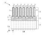
- the second grid 14 includes a grid layer 21, a metal layer 22, and a support substrate 23.
- the grid layer 21 has an effective function as an absorption grid, and includes an X-ray absorption part 26 and an X-ray transmission part 27, which are alternately perpendicular to the X-ray incident direction. Are arranged in various directions.
- the X-ray absorption part 26 is a columnar structure provided by extending linearly in the X direction, and is formed of a metal material having X-ray absorption. This metal material may be any material as long as it can absorb incident X-rays and can be formed by electroplating. In the present embodiment, the X-ray absorber 26 is formed of gold (Au).
- the X-ray transmission part 27 is provided between the X-ray absorption parts 26 and has a columnar plate-like structure provided by extending linearly in the X direction like the X-ray absorption part 26.
- the X-ray transmission part 27 is formed of a material having X-ray transparency. Since the X-ray transmission part 27 is formed by the remaining part obtained by etching the substrate, the X-ray transmission part 27 is formed of a material having low X-ray absorption ability and easy to etch.
- the X-ray transmission part 27 is made of silicon.
- An oxide film 27 a is provided on the outer peripheral portion of the X-ray transmission part 27.
- the X-direction width of the X-ray absorption unit 26 and the arrangement pitch of the X-ray absorption unit 26 and the X-ray transmission unit 27 (the total width of the X-ray absorption unit 26 and the X-ray transmission unit 27 in the X direction) 11 and the first grid 13, the distance between the first grid 13 and the second grid 14, the arrangement pitch of the X-ray absorption part and the X-ray transmission part of the first grid 13, and the like.
- the width of the X-ray absorption part is approximately 2 to 20 ⁇ m
- the arrangement pitch of the X-ray absorption part and the X-ray transmission part is 4 to 40 ⁇ m, which is twice as large.
- the thickness of the X-ray absorber in the Z direction is, for example, 100 to 200 ⁇ m in consideration of corneal X-ray vignetting irradiated from the X-ray source 11.
- the width of the X-ray absorption unit 26 is 2.5 ⁇ m
- the arrangement pitch of the X-ray absorption unit 26 and the X-ray transmission unit 27 is 5 ⁇ m
- the thickness of the X-ray absorption unit 26 is 100 ⁇ m. .
- the metal layer 22 is provided between the grid layer 21 and the support substrate 23.
- the grid layer 21 and the support substrate 23 are joined to ensure the stability of the second grid 14, and the X-ray absorption unit 26 is electroplated.
- the main function is to become a seed electrode when formed by.
- the metal layer 22 is formed with a three-layer structure of the first thin film 31, the second thin film 32, and the third thin film 33.
- the first thin film 31 is a thin film that functions as a sheath electrode when the X-ray absorbing portion 26 is formed by electroplating, and is formed of gold (Au) having a thickness of about 100 nm.
- the first thin film 31 may be made of any material as long as the formation of the X-ray absorbing portion 26 by electroplating is easy to proceed and the stability (resistance) to the plating solution is good.
- the first thin film 31 is made of platinum (Pt), nickel (Ni), titanium (Ti), chromium (Cr), silver (Ag), tantalum (Ta), tungsten (W), iridium ( You may form with metal films, such as Ir), palladium (Pd), rhodium (Rh), or an alloy containing any of these.
- metal films such as Ir), palladium (Pd), rhodium (Rh), or an alloy containing any of these.
- Gold and platinum have a relatively high X-ray absorption ability, but the first thin film 31 is formed so thin that it does not affect the X-ray absorption, so there is almost no loss of X-rays.
- the second thin film 32 is a thin film for strengthening the adhesion between the X-ray transmission part 27 and the first thin film 31, and is formed of titanium (Ti) having a thickness of about 10 nm.
- the second thin film 32 is formed of a metal having better adhesion to the X-ray transmission part 27 than at least the second layer 32, and has an X-ray absorption capability so as not to lose X-rays transmitted through the X-ray transmission part 27. What is necessary is just to form thinly in the range which can be manufactured stably stably with a low material, without impairing adhesiveness.
- titanium (Ti) is used as the second thin film 32.
- the second thin film 32 is made of, for example, chromium (Cr) having good adhesion to silicon. You may form with nickel (Ni) or the alloy containing these and titanium. Also, when these materials are used for the second thin film 32, the thickness may be about several nanometers to several tens of nanometers.
- the third thin film 33 is a thin film for stabilizing the bonding between the first thin film 31 and the support substrate 23, and is formed of, for example, aluminum (Al) or molybdenum (Mo) of about 500 nm.
- Al aluminum
- Mo molybdenum
- the silicon substrate 41 provided with the metal layer 22 and the support substrate 23 are joined by anodic bonding.
- the third thin film 33 is formed of a metal that is more stably bonded to the support substrate 23 than at least the first thin film 31 by anodic bonding, and so as not to lose the X-rays transmitted through the X-ray transmission part 27. What is necessary is just to form thinly in the range which can be manufactured stably and practically with a material with low X-ray absorption ability.
- the third thin film 33 is made of nickel (Ni), molybdenum (Mo), aluminum, tantalum (Ta), niobium (Nb), cobalt (Co), or these. An alloy containing any of them may be used. Even when these materials are used for the third thin film 33, the thickness may be about several tens nm to several hundreds nm.
- the support substrate 23 is a substrate for maintaining the structure of the grid layer 21 and is a glass substrate made of borosilicate glass.
- the support substrate 23 may be a substrate made of an ion conductive material to be bonded to the silicon substrate 41 provided with the metal layer 22 by anodic bonding, such as borosilicate glass (Pyrex (registered trademark) or Tempax (registered trademark)).
- borosilicate glass Pyrex (registered trademark) or Tempax (registered trademark)
- soda glass, potassium soda lead glass, aluminosilicate, beta alumina, zirconia, or the like can be used as the support substrate 23.
- the support substrate 23 is transparent to visible light or infrared light so that the bonding surface between the silicon substrate 41 provided with the metal layer 22 and the support substrate 23 can be observed through the support substrate 23. Is preferred.
- the radiation source grid 12 is configured in the same manner as the second grid 14 described above. However, the width of the X-ray absorption unit, the arrangement pitch of the X-ray absorption unit and the X-ray transmission unit, the overall size, and the like are determined by the arrangement of each grid.
- the method for manufacturing the absorption grid will be described using the second grid 14 as an example.
- the second grid 14 is manufactured in approximately five steps: a metal layer forming step, a bonding step, an etching step, an oxide film forming step, and an electroplating step.
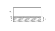
- a metal layer 22 is formed on one surface of a silicon substrate 41 (etching substrate) (metal layer forming step).
- the silicon substrate 41 later becomes the X-ray transmission part 27 of the grid layer 21.
- the metal layer 22 includes first to third thin films 31, 32, and 33, and is formed in order from the silicon substrate 41 side.
- the second thin film 32 is formed on the surface of the silicon substrate 41, and the first thin film 31 is formed on the second thin film 32.
- a third thin film 33 is further formed on the first thin film 31.
- vacuum deposition, sputtering, ion plating, CVD, or the like is used.
- the surface of the silicon substrate 41 is polished to a necessary extent and has a predetermined flatness in advance. If necessary, a polishing step for polishing the surface of the silicon substrate 41 may be added before the metal layer forming step.
- the film formation of the first to third thin films 31, 32, 33 is performed in the same vacuum chamber of one vapor deposition apparatus without breaking the vacuum. For this reason, this vapor deposition apparatus is provided with three types of vapor deposition sources capable of sequentially scattering the first to third thin films 31, 32, and 33, respectively.
- the first to third thin films 31, 32, 33 are formed using different vapor deposition apparatuses. However, if the vacuum is broken for each thin film 31, 32, 33, each thin film 31 is formed. , 32, 33, or an oxide film or the like may be formed on the surface of each thin film 31, 32, 33, and the flatness and adhesion of each thin film 31, 32, 33 may be reduced. These problems may cause early deterioration of the second grid 14 due to X-ray absorption by the X-ray absorbing unit 26 and the second grid 14 repeating thermal expansion. In this regard, as described above, the first to third thin films 31, 32, and 33 are continuously formed without breaking the vacuum with one vapor deposition apparatus, thereby flattening the thin films 31, 32, and 33 between them.
- the deterioration of the second grid 14 due to the flatness and adhesion between the thin films 31, 32, 33 can be prevented.
- Whether the first to third thin films 31, 32, 33 are formed without breaking the vacuum is determined by, for example, observing the interfaces of the thin films 31, 32, 33 with an SEM or the like. It can be determined by examining the presence or absence.
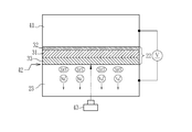
- the support substrate 23 is bonded to the metal layer 22 side of the silicon substrate 41 (bonding step).
- This bonding step is performed by anodic bonding.
- a predetermined DC voltage is applied between the silicon substrate 41 (metal layer 22) and the support substrate 23 while the silicon substrate 41 and the support substrate 23 are brought into contact with each other through the metal layer 22 and heated.
- the heating temperature is about 200 to 500 degrees
- the applied voltage is about 200 to 1000V.
- the applied voltage is negative on the support substrate 23 side and positive on the silicon substrate 41 side.
- This joining step may be performed in vacuum or in air.
- the bonding state is monitored by photographing the contact interface 42 with the imaging device 43 in the above-described bonding process.
- the imaging device 43 images the contact interface 42 from the back side of the support substrate 23 with visible light or infrared light.
- the support substrate 23 is not only ion-conductive for anodic bonding but also transparent to visible light or infrared light.
- the silicon substrate 41 is etched, and the columnar plate-like structure that is the X-ray transmitting portion 27 and the X-ray absorbing portion 26 are formed. Corresponding grooves 47 are formed (etching process).
- a resist is applied to the exposed surface of the silicon substrate 41, and this is exposed and developed to form a linear pattern corresponding to the arrangement pitch of the X-ray transmission part 27 and the X-ray absorption part 26.
- An etching mask is formed.
- the X-ray transmission part 27 and the groove 47 are formed by performing deep etching.
- Bosch process is an etching method using, for example, SF 6 gas for etching silicon (silicon substrate 41) and C 4 F 8 gas for forming a protective film.
- SF 6 gas for etching silicon
- C 4 F 8 gas for forming a protective film.
- etching is performed to expose the first thin film 31 of the metal layer 22 on the bottom of the groove 47.
- electroplating is possible if any part of the metal layer 22 is exposed at the bottom of the groove 47, so the second thin film 32 may be exposed.
- the second thin film 32 made of, for example, titanium is exposed at the bottom of the groove 47, titanium ions are eluted into the plating solution due to the difference in ionization tendency and contaminate the plating solution.
- the surface of the second thin film 32 is oxidized when it comes into contact with the atmosphere or a plating solution, but the adhesion between the oxidized second thin film 32 surface and gold deposited by electroplating is not good.
- the electroplating after removing the second thin film 32 exposed at the bottom of the groove 47 and exposing the first thin film 32. Since the first thin film 32 is formed of gold deposited by electroplating, it is resistant to plating solution, and surface oxidation does not occur even when exposed to the atmosphere or plating solution. Is good.
- an oxide film 27a is formed on the surface of the X-ray transmission part 27 as shown in FIG. 6 (oxide film formation process).
- the oxide film 27a functions as an insulating film in the electroplating process.
- the oxide film 27 a is provided on the surface of the X-ray transmission part 27, but another insulating material may be formed on the surface of the X-ray transmission part 27.
- the formation of an insulating film such as the oxide film 27a has an advantage that the generation of defective growth and voids can be suppressed in the electroplating step.
- the oxide film 27a After the formation of the oxide film 27a, as shown in FIG. 7, it is immersed in a plating solution, and gold is deposited and filled in the grooves 47 by electroplating to form the X-ray absorbing portion 26 (electroplating step).
- the cathode of the current terminal is connected to the metal layer 22.
- the end part of the silicon substrate 41 is simultaneously etched to expose the metal layer 22 to the outer peripheral part.
- the current terminal can be connected to the metal layer 22.
- the 1st thin film 31 is exposed among the metal layers 22 in an etching process as mentioned above, the 1st thin film 31 is a seed electrode more correctly.
- the plating solution used in the electroplating step is, for example, a cyan gold bath (KAu (CN) 2 ), and is adjusted to ph 6 to 8 by adding KH 2 PO 4 or KOH as a pH buffer material.
- the temperature of the plating solution is 25 to 70 ° C.
- the current density is 0.001 to 1 A / cm 2
- platinum plated titanium can be used for the anode 49.
- the various conditions of this electroplating process are examples, and are arbitrary if the X-ray absorption part 26 can be formed.
- the metal filling the groove 47 as the X-ray absorber 26 may be a metal other than gold as long as the X-ray can be shielded in consideration of the depth of the groove 47.
- the second grid 14 is manufactured by anodically bonding the silicon substrate 41 provided with the support substrate 23 and the metal layer 22 through the metal layer 22 and processing the joined body.
- the metal layer 22 functions as a seed electrode in the electroplating process, but the metal layer 22 is not formed only by the first thin film 31 as the seed electrode, but between the silicon substrate 41 and the support substrate 23.
- the third thin film 33 is formed of a material having good bonding properties by anodic bonding with respect to the support substrate 23, the first thin film 31 is brought into contact with the support substrate 23 so that the silicon substrate 41 and the support substrate 23 are anodes. Occurrence of bonding failure can be suppressed as compared with the case of bonding.
- the second thin film 32 and the third thin film 33 remain in the second grid 14 which is a finished product and perform the same function. That is, in the second grid 14, the second thin film 32 is firmly adhered to the metal layer 22 and the X-ray transmission part 26 formed by cutting out from the silicon substrate 41, and the third thin film 33 is bonded to the metal layer 22 by anodic bonding.
- the support substrate 23 is firmly and uniformly bonded. Therefore, since the X-ray absorption part 27 of the second grid 14 absorbs X-rays and has heat, the use of the X-ray imaging system 10 prevents the second grid 14 from repeating expansion and contraction to some extent.
- the second grid 14 is manufactured by bonding the substrates using diffusion bonding.
- diffusion bonding for example, in order to make the metal layer 22 have a three-layer structure, the second thin film 32 is provided on the surface of the silicon substrate 41, and the first thin film is provided on the surface of the support substrate 23 via the third thin film 33.
- the second grid 14 is manufactured by providing 31 by diffusion bonding.
- the same metal species are brought into contact with each other and bonded by mutual diffusion. Therefore, even if different metals are brought into contact as described above, bonding by diffusion bonding is usually not possible.
- the first thin film 31 is provided on the surface of the silicon substrate 41 via the second thin film 32, the third thin film 33 is provided on the surface of the support substrate 23, and these are joined by diffusion bonding to manufacture the second grid 14. The same applies to the case.
- the first to third thin films 31, 32, and 33 are formed by film formation rather than by bonding the interfaces. Adhesive strength is stronger than the case, and almost no poor bonding such as voids occurs. For this reason, the second grid 14 does not have a problem due to the bonding property between the second thin film 32 and the first thin film 31 or between the first thin film 31 and the third thin film 33.
- the bonding surface can be observed non-destructively and the bonding properties (diffusion / non-existence etc.) by diffusion bonding can be evaluated.
- the ultrasonic inspection apparatus is expensive and requires time for evaluation.
- the support substrate 23 is a glass substrate that is transparent to visible light or infrared light
- the silicon substrate 41 provided with the metal layer 22 and the support substrate 23 are bonded by anodic bonding.
- the glass substrate has a lower X-ray absorption capability than the silicon substrate, the X-ray loss in the portion of the second grid 14 excluding the X-ray absorption portion 26 can be suppressed by using the glass substrate as the support substrate 23. There is also a side effect.
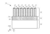
- the metal layer 22 has a three-layer structure including the first to third thin films 31, 32, 33, the two layers of the first thin film 31 and the third thin film 33 are formed like the second grid 51 shown in FIG.
- the metal layer 52 may be made of.
- the adhesion between the metal layer 52 and the X-ray transmission part 27 is inferior to that of the second grid 14.
- the bondability between the metal layer 52 and the support substrate 23 it is firmly bonded in the same manner as the second grid 14.
- the second thin film 32 is not provided, the loss of X-rays can be suppressed. Since there is the first thin film 31 that becomes a seed electrode in the electroplating process, the electroplating process can be performed in the same manner as described above.
- the metal layer may be a two-layer metal layer 54 of the second thin film 32 and the first thin film 31 as in the second grid 53 shown in FIG.
- the adhesion between the metal layer 54 and the support substrate 23 is inferior to the second grid 14 due to the absence of the third thin film 33, but the metal layer 54 and the X-ray transmission due to the presence of the second thin film 32.
- the adhesion of the portion 27 (silicon substrate 41) is as strong as the second grid 14 of the second embodiment described above.
- the third thin film 33 is not provided, the loss of X-rays can be suppressed. Since there is the first thin film 31 that becomes a seed electrode in the electroplating process, the electroplating process can be performed in the same manner as described above.
- the X-ray transmission part 27 is made of silicon (thermal expansion coefficient: 3.0 ⁇ 10 ⁇ 6 / ° C.), and the support substrate 23 is borosilicate glass (thermal expansion coefficient: 3.2 ⁇ 10). ⁇ 6 / ° C.), the difference in thermal expansion coefficient is small.
- the thermal expansion coefficient of 23 is not necessarily a close value.
- the second grid 14 is expanded when heated by anodic bonding in the bonding process or by temperature change when using the X-ray imaging system 10.
- the support substrate 23 may be warped or the support substrate 23 may be peeled off or cracked. Further, even if there is a slight bonding failure, stress due to a temperature change or the like concentrates on the bonding failure portion, so that particularly high-quality bonding is required even when anodic bonding is performed.
- the silicon substrate 57 and the ion conductive thin film 58 are bonded like the second grid 56 shown in FIG.
- the support substrate 59 may be used as the substrate. In this way, if the support substrate 59 is a bonding substrate of the silicon substrate 57 and the ion conductive thin film 58, the thermal expansion coefficients of the silicon substrate 41 (X-ray transmission part 27) and the support substrate 59 can be made closer. Damage to the support substrate 59 can be suppressed.
- the X-ray transmission part 27 is formed of another material such as GaAs.
- a substrate made of the material may be used instead of the silicon substrate 57.
- the same material as the material forming the X-ray transmission part 26 is used for a part of the support substrate 23 has been described.
- the substrate forming the X-ray transmission part 27 and the X-ray transmission part 27 and the support substrate 59 are used.
- a substrate made of other materials may be used as long as the difference in coefficient of thermal expansion can be reduced.
- the average thermal expansion coefficient of the entire grid layer 21 It is more preferable to reduce the difference in thermal expansion coefficient between the support substrate 59 and the support substrate 59.
- the ion conductive thin film 58 is formed of the same glass material as that of the support substrate 23. Since the ion conductive thin film 58 is a thin film for enabling the metal layer 22 and the support substrate 59 to be bonded by anodic bonding in the bonding process, the ion conductive thin film 58 may be formed thin within a range in which the metal layer 22 can be firmly bonded. it can. If the metal layer 22 can be bonded by anodic bonding, the ion conductive thin film 58 may have a thickness of about 1 to 2 ⁇ m, for example.
- the above-described problem due to the difference in thermal expansion coefficient between the silicon substrate 41 and the support substrate 23 can be solved by another method.
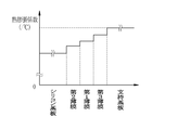
- the thermal expansion coefficients of the first to third thin films 31, 32, and 33 constituting the metal layer 22 are set as shown in FIG.
- the thermal expansion coefficient of the silicon substrate 41 is not less than the thermal expansion coefficient of the support substrate 23.
- the stress generated during heating or the like is relieved by the metal layer 22, so that the second grid 14 is not easily damaged.
- the support substrate 23 having a thermal expansion coefficient larger than that of the silicon substrate 41 is used.
- the thermal expansion coefficients of the thin films 31, 32, 33 be increased stepwise from the silicon substrate 41 side to the support substrate 23 side.
- the first to third thin films 31, 32, 33 are arranged so that the thermal expansion coefficient increases in the order of the silicon substrate 41, the second thin film 32, the first thin film 31, the third thin film 33, and the support substrate 23. Select material.
- thermal expansion coefficients of the first to third thin films 31, 32, 33 are increased stepwise from the silicon substrate 41 side to the support substrate 23 side, these thermal expansion coefficients are the thermal expansion coefficients of the silicon substrate 41. Even when the thermal expansion coefficient is not within the range of the support substrate 23 or less (for example, the thermal expansion coefficient of the third thin film 33 is larger than the thermal expansion coefficient of the support substrate 23), damage due to thermal expansion is not It can be suppressed by adjustment.
- the thermal expansion coefficients of the first to third thin films 31, 32, 33 are further increased as described above. More preferably, the materials of the first to third thin films 31, 32, 33 are determined so as to be between the thermal expansion coefficients of the silicon substrate 41 and the ion conductive thin film 58 (including the case where they are equal). Further, it is preferable to further increase the thermal expansion coefficient stepwise from the silicon substrate 41 to the ion conductive thin film 58.
- the thermal expansion coefficient between the silicon substrate 41 and the support substrate 23 since silicon and borosilicate glass have substantially the same thermal expansion coefficient, when the support substrate 23 made of the silicon substrate 41 and borosilicate glass is used. It is not always easy to set the thermal expansion coefficient of each thin film constituting the metal layer 22 to a value between the thermal expansion coefficients of these substrates. However, even in such a case, since the difference between the thermal expansion coefficients of the silicon substrate 41 and the support substrate 23 and the metal layer 22 is large, the silicon substrate 41 and the support substrate 23 may be damaged by the thermal expansion.
- the third thin film 33 may be formed of a material that is substantially equal to the thermal expansion coefficients of the silicon substrate 41 and the support substrate 23.
- the third thin film 33 is preferably made of, for example, Kovar or “42 alloy”. The same applies when the metal layer 22 has a three-layer structure of the first to third thin films 31, 32, and 33 and when the metal layer 22 has a two-layer structure of the first thin film 31 and the third thin film 33.
- Kovar is an alloy in which nickel and cobalt are blended with iron.
- nickel is 29% by weight
- cobalt is 17% by weight
- silicon is 0.2% by weight
- manganese is 0.3% by weight
- iron is 53.5% by weight.
- the coefficient of thermal expansion of Kovar is about 5.2 ⁇ 10 ⁇ 6 / ° C.
- 42 Alloy is an alloy in which nickel is mixed with iron, and contains, for example, 42 wt% nickel, 57 wt% iron, and a small amount of copper and manganese.
- the thermal expansion coefficient of “42 Alloy” is approximately 4.5 to 6.5 ⁇ 10 ⁇ 6 / ° C.
- the coefficient of thermal expansion of Kovar and “42 alloy” is larger than that of silicon and borosilicate glass, but it is possible to reduce problems caused by differences in the thermal expansion coefficients of the silicon substrate 41 and the support substrate 23 and the metal layer 22. Within a range approximately equal to the degree.
- the thickness is preferably about 30 nm in view of the balance between X-ray loss suppression and anodic bonding with the support substrate 23.
- the second grid 14 is formed in a flat plate shape and is mounted on the X-ray imaging system 10 in a flat plate shape. However, since the X-rays emitted from the X-ray source 11 spread in a cone beam shape, the flat grid plate is used. May cause vignetting in the X-rays at the periphery of the grid. In order to reduce vignetting, it is preferable to curve the second grid 14 or the like into a cylindrical surface (or a spherical surface) in accordance with the spread of X-rays, as shown in FIG. Since the second grid 14 has good adhesion between the metal layer 22 and the X-ray transmission part 27 and the bond between the metal layer 22 and the support substrate 23 is strong, it is difficult to be damaged even if it is curved in this way.
- the second grid 14 is taken as an example, the source grid 12 and its manufacturing method are the same as the above-described second grid 14 and its manufacturing method. The effect is the same.
- the source grid 12 and the second grid 14 are absorption grids, and the first grid 13 is a phase grid, but the first grid 13 may be an absorption grid.
- the configuration and manufacturing method are the same as described above. If at least one of the source grid 12, the first grid 13, and the second grid 14 uses the above-described absorption grid, the benefits can be obtained.
- the silicon substrate 41 is deepened by the Bosch process to form the grooves 47.
- the grooves 47 may be formed by other etching methods.
- the grooves 47 may be formed by anisotropic wet etching with different etching rates depending on the plane orientation of the silicon single crystal.
- the subject H is arranged between the X-ray source and the first grid, the subject H may be arranged between the first grid and the second grid. In this case as well, a phase contrast image is similarly generated.
- the radiation source grid is provided, but the radiation source grid may be omitted.
- the present invention is applicable not only to a radiographic imaging system for medical diagnosis but also to other radiographic systems for industrial use and nondestructive inspection.
- the grid of the present invention can also be applied to a scattered radiation removal grid that removes scattered radiation in X-ray imaging.
- the present invention can also be applied to a radiographic imaging system that uses gamma rays or the like in addition to X-rays.
Landscapes
- Life Sciences & Earth Sciences (AREA)
- Health & Medical Sciences (AREA)
- Engineering & Computer Science (AREA)
- Physics & Mathematics (AREA)
- Medical Informatics (AREA)
- High Energy & Nuclear Physics (AREA)
- Optics & Photonics (AREA)
- Molecular Biology (AREA)
- Veterinary Medicine (AREA)
- Nuclear Medicine, Radiotherapy & Molecular Imaging (AREA)
- Public Health (AREA)
- Pathology (AREA)
- Radiology & Medical Imaging (AREA)
- Biomedical Technology (AREA)
- Heart & Thoracic Surgery (AREA)
- Biophysics (AREA)
- Surgery (AREA)
- Animal Behavior & Ethology (AREA)
- General Health & Medical Sciences (AREA)
- Spectroscopy & Molecular Physics (AREA)
- General Engineering & Computer Science (AREA)
- Measurement Of Radiation (AREA)
- Apparatus For Radiation Diagnosis (AREA)
Description
本発明は、放射線画像撮影用の吸収型グリッド及びその製造方法と、このグリッドを用いた放射線画像撮影システムとに関する。
X線等の放射線(以下、X線を例にする)は、人体等の被検体に照射されると、被検体との相互作用により、強度と位相が変化する。従来普及しているX線撮影装置は、透過X線強度を画像化する。例えば、骨等はX線透過率が低く、筋肉等の組織はX線透過率が高いので、透過X線強度の分布を画像化すると、これらのX線透過率が異なる組織を識別することができる。このように、透過X線の強度を画像化したX線画像(以下、X線強度画像という)では、典型的にはX線透過率が高い組織は黒く、X線透過率が低い組織は白くなる。
X線強度画像によれば、X線透過率が異なる組織を識別することができるが、X線透過率が近い組織が隣接している場合には、これらの識別は容易ではない。例えば、軟骨等の軟部組織はX線透過率が高く、多くの場合、その周囲に隣接する組織や体液等もX線透過率が高いので、軟部組織はX線強度画像には写り難い。しかしながら、X線強度画像には写り難い組織にも病変は発生するので、これらもX線撮影により識別可能にすることが望まれている。
X線透過率が高くX線強度画像には写り難い組織も、透過X線に位相変化を与えていることが知られている。近年、透過X線の位相変化に基づいて被検体を画像化すること(位相イメージング)により、X線透過率が高い軟部組織等を識別可能なX線画像(以下、位相コントラスト画像という)を得るX線撮影システムが提案されている。
位相イメージングを行うX線撮影システムでは、透過X線の位相変化の情報を得るために、X線源とX線検出器との間に、少なくとも2つのグリッドを配置して被検体の撮影を行う。具体的には、X線源とX線検出器との間に第1グリッド及び第2グリッドを対向配置し、X線源から射出されたX線を、第1グリッドを通過させることにより、第1グリッドの自己像を有するX線像を生成する。このX線像の生成には、例えばタルボ効果が用いられる。そして、第1グリッドにより生成されたX線像に対して、第2グリッドの位置を面内方向に段階的に変化させながら、第1グリッドと第2グリッドを通過したX線像をX線検出器により撮影する。撮影により得られる複数の画像に基づいて位相コントラスト画像を生成することができる。このX線画像撮影方法は、縞走査法と呼ばれている。なお、X線源と第1グリッドとの間に、X線焦点を分散化し、X線像のコントラストを向上させるための線源グリッドが設けられることもある。
第1グリッドには、X線を部分的に吸収する吸収型グリッドと、部分的にX線の位相を変調して透過する位相型グリッドとのいずれかを用いることができる。一方、第2グリッドや線源グリッドには、吸収型グリッドを用いる必要がある。吸収型グリッドは、アスペクト比が高いことが必要である。
吸収型グリッドは、シリコン等の基板の表面に周期的にアスペクト比の高い溝を形成し、この溝に金(Au)等の金属材料(X線吸収材)を埋め込むことにより形成される。このように、アスペクト比が高い溝に金属材料をほぼ一様に埋め込む方法としては、例えば電気メッキが用いられるが、この電気メッキを行うためには、溝の底部にシーズ電極を設ける必要がある。
電気メッキを用いた吸収型グリッドの製造方法として、金属薄膜が表面に成膜された2つの基板を、金属薄膜同士を向かい合わせて加圧及び加熱して接合(いわゆる拡散接合)し、一方の基板にアスペクト比の高い複数の溝を形成して、その底に金属薄膜を露呈させ、この金属薄膜をシーズ電極として電気メッキを行う方法が知られている(例えば、特開2011-162854号公報,国際公開第2011/122506号を参照)。
拡散接合は、母材である基板に塑性変形が生じない程度に加圧及び加熱することにより、接触面間の原子の拡散を利用して接合する方法である。このため、拡散接合による接合の状態は、接合する表面の平坦性や清浄性に大きく影響される。すなわち、接合面に凹凸やゴミがあると未接合部分(ボイド等)が発生して、接合不良や接合後の剥離が発生しやすい。このため、シーズ電極の形成には、拡散接合よりも接合不良が生じにくい接合方法を採用することが望ましい。
国際公開第2011/122506号には、拡散接合の代わりに、陽極接合を用いることも記載されている。陽極接合は、加熱しながら電圧を印加することにより、例えば、シリコン等の半導体とガラス(または金属とガラス)を接合する接合方法である。このため、2つの基板の一方の表面に金属薄膜を成膜し、これらを陽極接合し、一方の基板にアスペクト比の高い複数の溝を形成して、その底に金属薄膜を露呈させ、この金属薄膜をシーズ電極として電気メッキを行えば、吸収型グリッドを製造可能である。しかし、接合面に凹凸やゴミがあると未接合部分(ボイド等)が発生して、接合不良や接合後の剥離が発生しやすいことは、拡散接合を用いる場合と同様である。
本発明は、2つの基板の境界面に、接合不良や接合後の剥離が生じることを防止する放射線画像撮影用吸収型グリッド及びその製造方法を提供することを目的とする。
また、この放射線画像撮影用吸収型グリッドを用いた放射線撮影システムを提供することを目的とする。
また、この放射線画像撮影用吸収型グリッドを用いた放射線撮影システムを提供することを目的とする。
本発明の放射線画像撮影用吸収型グリッドは、グリッド層、支持基板、金属層を備える。グリッド層は、放射線を吸収する放射線吸収部と放射線を透過する放射線透過部が放射線の入射方向に対して垂直な方向に交互に配列された構造を有する。支持基板は、少なくともグリッド層側の面にイオン導電性材料を有し、グリッド層を支持する。金属層は、グリッド層と支持基板の間に設けられ、グリッド層の放射線透過部に対しては成膜により密着され、支持基板に対しては陽極接合により接合される。さらに、金属層は、第1薄膜と、第2薄膜または第3薄膜を含む。第1薄膜は、放射線吸収部を電気メッキにより形成するときにシーズ電極として機能する金属薄膜である。第2薄膜は、第1薄膜よりも放射線透過部に対する密着性が良く、第1薄膜とグリッド層の間に設けられる金属薄膜である。第3薄膜は、前記陽極接合において第1薄膜よりも支持基板に対する接合性が良く、第1薄膜と前記支持基板の間に設けられる金属薄膜である。
金属層は、第2薄膜、第1薄膜、第3薄膜の3層構造であることが好ましい。
第1薄膜は、第2薄膜を介さずに放射線吸収部と直接接触していることが好ましい。
放射線透過部の表面に絶縁膜が形成されていることが好ましい。
第2薄膜が、チタン、クロム、ニッケル、またはこれらのいずれかを含む合金であることが好ましい。
第1薄膜が、金、白金、イリジウム、パラジウム、ロジウム、またはこれらのいずれかを含む合金であることが好ましい。
第3薄膜が、アルミニウム、ニッケル、モリブデン、タングステン、またはこれらのいずれかを含む合金であることが好ましい。
支持基板の熱膨張係数が放射線透過部の熱膨張係数よりも小さい場合に、第1薄膜、第2薄膜及び第3薄膜の熱膨張係数は、支持基板の熱膨張係数以上でかつ放射線透過部の熱膨張係数以下であることが好ましい。
支持基板の熱膨張係数が放射線透過部の熱膨張係数よりも大きい場合に、第1薄膜、第2薄膜及び第3薄膜の熱膨張係数は、支持基板の熱膨張係数以下でかつ放射線透過部の熱膨張係数以上であり、放射線透過部、第2薄膜、第1薄膜、第3薄膜、支持基板の順に段階的に熱膨張係数が大きいことが好ましい。
支持基板は、イオン導電性基板であることが好ましい。
支持基板は、放射線透過部と同じ材料で形成された基板と、この基板上に設けられたイオン導電性薄膜とからなり、イオン導電性薄膜によって金属層に接合していることが好ましい。
本発明の放射線画像撮影用吸収型グリッドの製造方法は、金属層形成工程、接合工程、エッチング工程、電気メッキ工程を備える。金属層形成工程は、放射線を透過する放射線透過部の材料からなるエッチング基板の一方の表面に、電気メッキ工程においてシーズ電極になる第1薄膜に加えて、第1薄膜の成膜前または成膜後に、第2薄膜または第3薄膜のうち少なくとも一方を成膜し、少なくとも2種類の金属薄膜を有する金属層を形成する。第2薄膜は、シーズ電極よりもエッチング基板との密着性が良く、第1薄膜と前記エッチング基板の間に成膜される。第3薄膜は、シーズ電極よりも支持基板との接合性が良く、第1薄膜上に成膜される。接合工程は、金属層に支持基板を接触させて陽極接合をすることにより、金属層が形成されたエッチング基板と支持基板の接合体を形成する。エッチング工程は、接合体のエッチング基板を所定パターンにエッチングし、放射線を吸収する放射線吸収部になる溝と放射線透過部を形成し溝の底部に金属層を露呈させる。電気メッキ工程は、溝に露呈された前記金属層をシーズ電極として、電気メッキにより溝に放射線を吸収する放射線吸収材を埋め込む。
金属層形成工程では、エッチング基板上に、第2薄膜と、第1薄膜と、第3薄膜をこの順に成膜し、3種の金属薄膜からなる前記金属層を形成することが好ましい。
金属層形成工程では、複数の金属薄膜を全て同じ成膜装置で真空を破らずに成膜することが好ましい。
本発明の放射線画像撮影システムは、放射線源から照射される放射線を、吸収型グリッドを介して撮影して位相コントラスト画像を生成する放射線画像撮影システムであり、吸収型グリッドが、グリッド層、支持基板、金属層を備える。グリッド層は、放射線を吸収する放射線吸収部と放射線を透過する放射線透過部が放射線の入射方向に対して垂直な方向に交互に配列された構造を有する。支持基板は、少なくともグリッド層側の面にイオン導電性材料を有し、グリッド層を支持する。金属層は、グリッド層と支持基板の間に設けられ、グリッド層の放射線透過部に対しては成膜により密着され、支持基板に対しては陽極接合により接合される。さらに、金属層は、第1薄膜と、第2薄膜または第3薄膜を含む。第1薄膜は、放射線吸収部を電気メッキにより形成するときにシーズ電極として機能する金属薄膜である。第2薄膜は、第1薄膜よりも放射線透過部に対する密着性が良く、第1薄膜とグリッド層の間に設けられる金属薄膜である。第3薄膜は、前記陽極接合において第1薄膜よりも支持基板に対する接合性が良く、第1薄膜と前記支持基板の間に設けられる金属薄膜である。
本発明の放射線画像撮影用吸収型グリッドは、シーズ電極の前後の少なくとも一方に、シーズ電極よりも放射線透過部との密着性が良い金属薄膜、または陽極接合においてシーズ電極よりも支持基板との接合性が良い金属薄膜のいずれかを含むので、シーズ電極を形成した境界面における接合不良による剥離等の不具合が生じ難い。
図1に示すように、X線画像撮影システム10は、X線照射方向であるZ方向に沿って、X線源11、線源グリッド12、第1グリッド13、第2グリッド14、及びX線画像検出器15を備える。
X線源11は、回転陽極型のX線管(図示せず)と、X線の照射野を制限するコリメータ(図示せず)とを有し、被検体HにX線を放射する。
線源グリッド12及び第2グリッド14は、X線を部分的に吸収する吸収型グリッドであり、直線状のX線吸収部とX線透過部が交互に配列されている。第1グリッド13は基板の凹凸構造により所定位相差(例えばπまたはπ/2)を発生させる位相型グリッドである。各グリッド12~14は、Z方向においてX線源11に対向配置されており、いずれも格子線がX方向に沿って設けられている。
線源グリッド12と第1グリッド13との間には、被検体Hが配置可能な間隔が設けられている。第1グリッド13と第2グリッド14との距離は、例えばタルボ距離に設定する。タルボ距離とは、第1グリッド13を通過したX線が、タルボ効果により第1グリッド13の自己像を生成する距離である。
X線画像検出器15は、半導体回路を用いたフラットパネル検出器であり、第2グリッド14の背後に配置されている。
X線源11から放射されたX線は、線源グリッド12のX線吸収部によって部分的に遮蔽されることにより、Y方向に関する実効的な焦点サイズが縮小され、Y方向に配列された多数のライン状のX線が形成される。各ライン状のX線は、被検体Hを通過する際に位相が変化する。この各X線が第1グリッド13を通過することにより、被検体Hの屈折率と透過光路長とから決定される被検体Hの透過位相情報を反映した縞画像(第1グリッド13の自己像)が形成される。各ライン状のX線により生成された縞画像は、第2グリッド14に投影され、第2グリッド14の位置で重なり合う。
縞画像は、第2グリッド14により部分的に遮蔽されることにより強度変調される。本実施形態では、縞走査法を用いて位相コントラスト画像を生成する。すなわち、第1グリッド13に対して第2グリッド14を間欠移動させるとともに、その停止中に、X線源11から被検体HにX線を照射してX線画像検出器15により撮影を行う。この間欠移動は、格子ピッチを等分割(例えば、5分割)した一定の走査ピッチでY方向に行う。
X線画像検出器15の各画素の画素データの強度変化を表す強度変調信号の位相ズレ量(被検体Hがある場合とない場合とでの位相のズレ量)を算出することにより、位相微分画像が得られる。位相微分画像は、被検体HでのX線の屈折角度の分布に対応する。この位相微分画像をX方向に沿って積分することにより、位相コントラスト画像が得られる。
以下、第2グリッド14を例にして、吸収型グリッドの構造を説明する。図2に示すように、第2グリッド14は、グリッド層21、金属層22、支持基板23を備える。
グリッド層21は、吸収型グリッドとしての実効的な機能を担っている層であり、X線吸収部26とX線透過部27を有し、これらが交互にX線の入射方向に対して垂直な方向に配列されて形成されている。
X線吸収部26は、X方向に直線状に延伸して設けられた柱板状構造であり、X線吸収性を有する金属材料で形成される。この金属材料は、入射X線を吸収し、電気メッキで形成することができれば任意の材料で良い。本実施形態では、X線吸収部26を金(Au)で形成している。
X線透過部27は、X線吸収部26の間に設けられ、X線吸収部26と同様にX方向に直線状に延伸して設けられた柱板状構造である。但し、X線透過部27は、X線透過性を有する材料で形成される。X線透過部27は、基板をエッチングした残存部により形成するので、X線吸収能が低く、エッチングが容易な材料で形成される。本実施形態では、X線透過部27はシリコンで形成されている。なお、X線透過部27の外周部分には酸化膜27aが設けられている。
X線吸収部26のX方向の幅や、X線吸収部26とX線透過部27の配列ピッチ(X線吸収部26とX線透過部27のX方向の合計幅)は、X線源11と第1グリッド13との間の距離、第1グリッド13と第2グリッド14との距離、及び第1グリッド13のX線吸収部とX線透過部の配列ピッチ等に応じて決定される。例えば、X線吸収部の幅は、およそ2~20μmであり、X線吸収部とX線透過部の配列ピッチはその倍の4~40μmである。X線吸収部のZ方向の厚みは、X線源11から照射されるコーンビーム状のX線のケラレを考慮して、例えば100~200μmとなっている。本実施形態の第2グリッド14は、X線吸収部26の幅は2.5μm、X線吸収部26とX線透過部27の配列ピッチは5μm、X線吸収部26の厚みは100μmである。
金属層22は、グリッド層21と支持基板23の間に設けられ、グリッド層21と支持基板23を接合して第2グリッド14の安定性を確保することと、X線吸収部26を電気メッキにより形成するときにシーズ電極になることが主な機能である。
このため、金属層22は、第1薄膜31、第2薄膜32、第3薄膜33の3層構造で形成されている。
第1薄膜31は、X線吸収部26を電気メッキで形成するときにシーズ電極として機能する薄膜であり、100nm程度の厚さの金(Au)で形成されている。第1薄膜31は、電気メッキによるX線吸収部26の形成が進みやすく、メッキ液に対する安定性(耐性)が良いものであれば、材料は任意である。例えば、金の他に、第1薄膜31を白金(Pt)や、ニッケル(Ni)、チタン(Ti)、クロム(Cr)、銀(Ag)、タンタル(Ta)、タングステン(W)、イリジウム(Ir)、パラジウム(Pd)、ロジウム(Rh)等の金属膜、あるいはこれらのいずれかを含む合金で形成しても良い。これらの各種金属の中でも、第1薄膜31には、金、白金、イリジウム、パラジウム、ロジウム、あるいはこれらのいずれかを含む合金を用いることが好ましく、特に、イオン化傾向が小さくメッキ液耐性が高い金または白金を用いることが特に好ましい。金や白金はX線吸収能が比較的高いが、第1薄膜31は、X線の吸収が影響しない程度に薄く形成されているので、X線の損失はほぼない。
第2薄膜32は、X線透過部27と第1薄膜31の密着を強化するための薄膜であり、10nm程度の厚さのチタン(Ti)で形成されている。第2薄膜32は、少なくとも第2層32よりもX線透過部27との密着性が良い金属で形成され、X線透過部27を透過するX線を損失しないように、X線吸収能が低い材料で、かつ、密着性を損なわず、現実的に安定して製造できる範囲内で薄く形成されていれば良い。本実施形態では、第2薄膜32としてチタン(Ti)を用いているが、X線透過部27をシリコンで形成する場合、第2薄膜32を例えばシリコンとの密着性が良いクロム(Cr)やニッケル(Ni)、またはこれらやチタンを含む合金で形成してもよい。また、第2薄膜32にこれらの材料を用いる場合も、その厚さは数nm~数十nm程度にすればよい。
第3薄膜33は、第1薄膜31と支持基板23の接合を安定させるための薄膜であり、例えば500nm程度のアルミニム(Al)またはモリブデン(Mo)で形成されている。後述するように、金属層22を設けたシリコン基板41と支持基板23とは陽極接合によって接合される。このため、第3薄膜33は、陽極接合によって少なくとも第1薄膜31よりも支持基板23と安定して接合される金属で形成され、X線透過部27を透過するX線を損失しないように、X線吸収能が低い材料で、かつ、現実的に安定して製造できる範囲内で薄く形成されていれば良い。本実施形態では、第3薄膜33としてアルミニウムを用いるが、第3薄膜33はニッケル(Ni)やモリブデン(Mo)、アルミニウム、タンタル(Ta)、ニオブ(Nb)、コバルト(Co)、あるいはこれらのいずれかを含む合金でも良い。第3薄膜33にこれらの材料を用いる場合も、その厚さは数十nm~数百nm程度にすれば良い。
支持基板23は、グリッド層21の構造を維持するための基板であり、ホウケイ酸ガラスからなるガラス基板である。支持基板23は、金属層22を設けたシリコン基板41と陽極接合により接合とするイオン導電性材料からなる基板であればよく、ホウケイ酸ガラス(パイレックス(登録商標)やテンパックス(登録商標))の他には、ソーダガラス、カリウムソーダ鉛ガラス、アルミノシリケート、ベータアルミナ、ジルコニア等を支持基板23として用いることができる。なお、後述するように、支持基板23は、金属層22を設けたシリコン基板41と支持基板23の接合面を、支持基板23を通して観察できるように、可視光または赤外線に対して透明であることが好ましい。
線源グリッド12は、上述の第2グリッド14と同様に構成される。但し、X線吸収部の幅や、X線吸収部とX線透過部の配列ピッチ、全体としての大きさ等は各グリッドの配置等によって決定される。
次に、第2グリッド14を例にして、吸収型グリッドの製造方法を説明する。第2グリッド14は、以下に説明するように、金属層形成工程、接合工程、エッチング工程、酸化膜形成工程、電気メッキ工程の概ね5工程で製造される。
図3に示すように、まず、シリコン基板41(エッチング基板)の一方の表面に金属層22を成膜する(金属層形成工程)。シリコン基板41は、後にグリッド層21のX線透過部27になる。金属層22は、第1~第3薄膜31,32,33からなり、シリコン基板41側から順に成膜が行われる。具体的には、シリコン基板41の表面に第2薄膜32を成膜し、この第2薄膜32上に第1薄膜31を成膜する。そして、第1薄膜31上にさらに第3薄膜33を成膜する。これらの成膜には、真空蒸着、スパッタリング、イオンプレーティング、CVD等を用いる。なお、シリコン基板41の表面は必要な程度に研磨され、予め所定の平坦性を有している。必要であれば、金属層形成工程の前にシリコン基板41の表面を研磨する研磨工程を加えて良い。
第1~第3薄膜31,32,33の成膜は、1台の蒸着装置の同じ真空チャンバ内において、1度も真空を破らずに行われる。このため、この蒸着装置には、第1~第3薄膜31,32,33をそれぞれ順に飛散させることが可能な3種の蒸着源を設ける。
第1~第3薄膜31,32,33の成膜をそれぞれ異なる蒸着装置を用いて行うことも可能であるが、各薄膜31,32,33の成膜毎に真空を破ると、各薄膜31,32,33にゴミが付着したり、各薄膜31,32,33の表面に酸化膜等が形成されたりし、各薄膜31,32,33の平坦性や密着性が低下することがある。これらの不具合は、X線吸収部26でX線を吸収して第2グリッド14が熱膨張を繰り返すこと等により、第2グリッド14の早期劣化の原因になることがある。この点、上述のように第1~第3薄膜31,32,33の成膜を、1台の蒸着装置で真空を破らずに連続して行うことで各薄膜31,32,33間の平坦性や密着性を確保することができるとともに、各薄膜31,32,33間の平坦性や密着性に起因する第2グリッド14の劣化を防止することができる。第1~第3薄膜31,32,33が真空を破らずに成膜されたものであるか否かは、例えば、SEM等で各薄膜31,32,33の界面を観察し、酸化膜の有無等を調べることにより判断可能である。
続いて、図4に示すように、シリコン基板41の金属層22側に支持基板23を接合する(接合工程)。この接合工程は、陽極接合により行う。具体的には、シリコン基板41と支持基板23とを金属層22を介して接触させ、これらを加熱しつつ、シリコン基板41(金属層22)と支持基板23の間に所定の直流電圧を印加する。例えば、加熱温度は200~500度程度であり、印加電圧は200~1000V程度である。また、印加電圧は支持基板23側が負であり、シリコン基板41側が正である。この接合工程は、真空中で行なっても良いし、空気中で行なっても良い。
このように、金属層22を介して接触させたシリコン基板41と支持基板23を加熱しながら電圧を印加すると、ガラス基板である支持基板23内では、金属層22との接触界面42近傍において、ナトリウムイオン(Na+)やホウ素イオン(B3+)等が金属層22から遠ざかる向きに引き離される。加熱状態において、ガラスは導電性がある固体電解質とみなすことができ、正の電荷を有するナトリウムイオンは極めて動きやすくなる。このため、支持基板23内のナトリウムイオンは陰極側に集まり、金属層22と支持基板23の界面には空間電荷領域が形成される。電圧降下のほとんどがこの空間電荷領域に加わるので、支持基板23と金属層22の間に強い電界が加わり、静電力によって強く引き合って接触し、表面原子が共有結合を作る。具体的には、支持基板23の構造そのものである一酸化ケイ素イオン(SiO-)と、第3薄膜33の金属イオンが共有結合を形成する。これにより、シリコン基板41と支持基板23は金属層22を介して接合される。
接合工程では、金属層22と支持基板23が結合されるときに電流が発生する。このため、シリコン基板41と支持基板23間に流れる電流量により、金属層22と支持基板23の接合の進行度合いを大まかに知ることができる。但し、この電流の監視だけでは接合のムラ等、接合状態の評価まではできないので、上述の接合工程では撮像装置43によって接触界面42を撮影して接合状態を監視する。撮像装置43は、可視光または赤外線により、支持基板23の裏面側から接触界面42を撮影する。このため、支持基板23は、陽極接合のためにイオン導電性であるだけでなく、さらに、可視光または赤外線に対して透明であることが好ましい。
図5に示すように、接合工程で形成されたシリコン基板41と支持基板23の接合体は、シリコン基板41がエッチングされ、X線透過部27である柱板状構造とX線吸収部26に対応する溝47が形成される(エッチング工程)。
具体的には、まず、露呈されたシリコン基板41の表面にレジストを塗布し、これを露光及び現像して、X線透過部27及びX線吸収部26の配列ピッチに対応する直線状パターンのエッチングマスクを形成する。そして、深堀用のエッチングをすることにより、X線透過部27と溝47を形成する。
深堀用のエッチングには、例えば、ボッシュプロセスと呼ばれるドライエッチングが好適である。ボッシュプロセスは、例えば、シリコン(シリコン基板41)をエッチングするSF6ガスと、保護膜を形成するためのC4F8ガスとを用いるエッチング方法である。SF6ガスでシリコン基板41をエッチングすると深さ方向だけでなく、横方向にもエッチングが進行するため、これだけでは第2グリッド14のようにアスペクト比が大きい溝を形成することができない。このため、ボッシュプロセスでは、SF6ガスで所定時間エッチングした後、C4F8ガスに切り換え、プラズマにより生成されるCFnのポリマーを溝47内に付着させて保護膜を形成する。そして、再びSF6ガスによりエッチングを行う。このボッシュプロセスによれば、底面に比べて側面のエッチング速度は低いため、ほぼ底面だけをエッチングして溝47を深堀りすることができる。
また、エッチング工程では、さらに溝47の底に金属層22の第1薄膜31を露呈させるエッチングを行う。なお、電気メッキ工程では、溝47の底に金属層22のいずれかの部分が露呈していれば電気メッキが可能であるので、第2薄膜32が露呈されていても良い。しかし、例えばチタンからなる第2薄膜32が溝47の底に露呈していると、イオン化傾向の相違によりチタンイオンがメッキ液中に溶出してメッキ液を汚染する。また、第2薄膜32は大気やメッキ液と接触すると表面が酸化されるが、酸化した第2薄膜32表面と電気メッキにより析出する金の密着性は良くない。このため、溝47の底に露呈された第2薄膜32を除去し、第1薄膜32を露呈させてから電気メッキを行うことが好ましい。第1薄膜32は、電気メッキによって析出させる金で形成されているので、メッキ液耐性があり、かつ、大気やメッキ液に露呈されても表面酸化が起こらないので、析出する金との密着性が良い。
上述のエッチング工程により、X線透過部27と溝47を形成した後は、図6に示すように、X線透過部27の表面に酸化膜27aを形成する(酸化膜形成工程)。酸化膜27aは、電気メッキ工程で絶縁膜として機能する。ここでは、X線透過部27の表面に酸化膜27aを設けているが、X線透過部27の表面に他の絶縁性の材料を成膜しても良い。この酸化膜形成工程を省略することも可能であるが、酸化膜27a等の絶縁膜を形成することにより、電気メッキ工程において成長不良やボイドの発生が抑えられるという利点がある。
酸化膜27aの形成後は、図7に示すように、メッキ液に浸漬して、電気メッキにより溝47に金を析出させて充填し、X線吸収部26を形成する(電気メッキ工程)。この電気メッキ工程では、電流端子の陰極が金属層22に接続される。例えば、エッチング工程でX線透過部27及び溝47を形成するときにシリコン基板41の端部を同時にエッチングして、外周部分に金属層22を露呈させておくことで、この露呈された外周部分で電流端子を金属層22に接続することができる。
このように電流端子を接続し、メッキ液に浸漬した状態で金属層22と陽極49間に通電すると、金属層22がシーズ電極となり、メッキ液に含まれる金イオン(Au+)が露呈された金属層22の表面に接触することにより金(Au)が析出する。このため、溝47には金が充填され、X線吸収部26が形成される。この電気メッキ工程により、グリッド21、及び全体として第2グリッド14が完成する。
なお、前述のようにエッチング工程では金属層22のうち第1薄膜31が露呈されるので、より正確には第1薄膜31がシーズ電極である。
また、電気メッキ工程で用いるメッキ液は、例えばシアン金浴(KAu(CN)2)であり、pH緩衝材としてKH2PO4,KOHを添加することによりph6~8に調節される。例えば、メッキ液の温度は25~70℃、電流密度は0.001~1A/cm2とし、陽極49には白金メッキされたチタンを用いることができる。この電気メッキ工程の諸条件は一例であり、X線吸収部26を形成することができれば任意である。また、電気メッキ工程において、X線吸収部26として溝47に充填する金属も、溝47の深さを考慮して、X線を遮蔽することができれば金以外の金属を用いても良い。
以上のように、第2グリッド14は、支持基板23と金属層22を設けたシリコン基板41を、金属層22を介して陽極接合し、その接合体を加工して製造される。そして、金属層22は電気メッキ工程でシーズ電極として機能するものであるが、金属層22はシーズ電極である第1薄膜31だけで形成されるのではなく、シリコン基板41及び支持基板23の間にそれぞれ第2薄膜32と第3薄膜33を備えている。第2薄膜32は、シリコン基板41との密着性が良い材料で形成されているので、第1薄膜31をシリコン基板41上に成膜する場合よりも接合不良の発生を抑えることができる。また、第3薄膜33は、支持基板23に対して陽極接合による接合性が良い材料で形成されているので、第1薄膜31を支持基板23に接触させてシリコン基板41と支持基板23を陽極接合する場合よりも接合不良の発生を抑えることができる。
第2薄膜32及び第3薄膜33は完成品である第2グリッド14においても残り、同様の機能を果たす。すなわち、第2グリッド14において、第2薄膜32はシリコン基板41から削り出して形成されたX線透過部26と金属層22を強固に密着させ、第3薄膜33は陽極接合によって金属層22と支持基板23を強固にむらなく接合する。したがって、第2グリッド14のX線吸収部27はX線を吸収して熱を持つので、X線画像撮影システム10の使用によって第2グリッド14がある程度の膨張と収縮を繰り返することが避けられないが、こうした膨張や収縮の繰り返されても、第2薄膜32と第3薄膜33があることによってグリッド層26や支持基板23が剥離してしまう等の不具合が生じ難い。また、上述のように構成される第2グリッド14を用いたX線画像撮影システム10は、第2グリッド14の不良や経時劣化を原因とする故障が生じ難い。
さらに、拡散接合を利用して基板を接合して第2グリッド14を製造する場合と比較する。拡散接合を利用する場合、例えば、金属層22を3層構造にするために、シリコン基板41の表面に第2薄膜32を設け、支持基板23の表面に第3薄膜33を介して第1薄膜31を設け、これらを拡散接合により接合して第2グリッド14を製造することが考えられる。しかし、拡散接合は、同じ金属種同士を接触させ、その相互拡散により接合を行うものであるので、上述のように異種金属間を接触させても、通常、拡散接合では接合できない。また、シリコン基板41の表面に第2薄膜32を介して第1薄膜31を設け、支持基板23の表面に第3薄膜33を設け、これらを拡散接合により接合して第2グリッド14を製造する場合も同様である。
この点、上述の第2グリッド14の製造方法によれば、第1~第3薄膜31,32,33は、界面を接合するのではなく、成膜して形成しているので、拡散接合による場合よりも密着力は強く、ボイド等の接合不良もほぼ発生しない。このため、第2薄膜32と第1薄膜31や、第1薄膜31と第3薄膜33の接合性により第2グリッド14に不具合が生じることがない。
また、拡散接合は、金属と金属を接合するものであるため、接合時あるいは接合後に接合面を観察することは容易ではない。超音波検査によれば接合面を非破壊に観察して、拡散接合による接合性(ボイドの有無等)を評価することもできるが、超音波検査装置は高価であり、評価に時間も要する。これに対して、上述実施形態のように、支持基板23を可視光または赤外線に対して透明なガラス基板とし、陽極接合によって、金属層22を設けたシリコン基板41と支持基板23を接合すれば、接合時あるいは接合後に、支持基板23側から接合面(第3薄膜33と支持基板23の界面42)を観察してその接合性を評価し、不良を分別することが容易である。
なお、ガラス基板はシリコン基板よりもX線吸収能が低いので、支持基板23としてガラス基板を用いることにより、第2グリッド14のX線吸収部26を除く部分におけるX線損失を抑えることができるという副次的な効果もある。
なお、金属層22を第1~第3薄膜31,32,33からなる3層構造としたが、図8に示す第2グリッド51のように、第1薄膜31と第3薄膜33の2層からなる金属層52にしても良い。この場合、第2薄膜32がないことにより、第2グリッド14と比較すれば金属層52とX線透過部27(シリコン基板41)の密着性が劣るが、第3薄膜33があることにより、金属層52と支持基板23の接合性については第2グリッド14と同様に強固に接合される。また、第2薄膜32を設けない分、X線の損失を抑えることができる。電気メッキ工程でシーズ電極になる第1薄膜31があるので、電気メッキ工程は前述と同様に行うことができる。
同様に、図9に示す第2グリッド53のように、金属層を第2薄膜32と第1薄膜31の2層からなる金属層54にしても良い。この場合、第3薄膜33がないことにより、第2グリッド14と比較すれば金属層54と支持基板23の密着性が劣るが、第2薄膜32があることにより、金属層54とX線透過部27(シリコン基板41)の密着性については上述の第2実施形態の第2グリッド14と同様に強固である。また、第3薄膜33を設けない分、X線の損失を抑えることができる。電気メッキ工程でシーズ電極になる第1薄膜31があるので、電気メッキ工程は前述と同様に行うことができる。
なお、第2グリッド14は、X線透過部27がシリコン(熱膨張係数:3.0×10⁻⁶/℃)からなり、支持基板23がホウケイ酸ガラス(熱膨張係数:3.2×10-6/℃)であるため熱膨張係数の差は小さいが、支持基板23に他のイオン導電性材料を用いる場合等、これらの組み合わせ以外の材料を用いるときには、X線透過部27と支持基板23の熱膨張係数が近い値であるとは限らない。X線透過部27と支持基板23の熱膨張係数に差があると、接合工程における陽極接合時の加熱や、X線画像撮影システム10使用時の温度変化等によって膨張すると、第2グリッド14が反ってしまったり、さらには支持基板23がはがれたり、割れたりしてしまうことがある。また、僅かな接合不良があるだけでも、温度変化等による応力が接合不良箇所に集中するので、陽極接合をする場合でも、特に高品質な接合が要求される。
このため、シリコン基板41と支持基板23に熱膨張係数の差が大きい材料を用いる場合には、例えば、図10に示す第2グリッド56のように、シリコン基板57とイオン導電性薄膜58を接合した基板を支持基板59にしても良い。このように、支持基板59をシリコン基板57とイオン導電性薄膜58の接合基板にしておけば、シリコン基板41(X線透過部27)と支持基板59の熱膨張係数を近づけることができるので、支持基板59の破損等が抑えられる。
シリコン基板57は、支持基板59の熱膨張係数を、グリッド層21を形成するシリコン基板41と熱膨張係数を合わせるための基板なので、X線透過部27をGaAs等他の材料で形成する場合には、その材料からなる基板をシリコン基板57の替りに用いれば良い。また、ここではX線透過部26を形成する材料と同じ材料を支持基板23の一部に用いる例を挙げたが、X線透過部27を形成する基板及びX線透過部27と支持基板59との熱膨張係数の差を緩和することができれば、その他の材料からなる基板を用いても良い。さらに、X線透過部27を形成するシリコン基板41と支持基板59の熱膨張係数の差を緩和するだけでなく、X線吸収部26を考慮してグリッド層21全体の平均的な熱膨張係数と支持基板59の熱膨張係数の差を緩和することがより好ましい。
イオン導電性薄膜58は、支持基板23と同様のガラス材料で形成する。イオン導電性薄膜58は、接合工程において陽極接合により金属層22と支持基板59を接合できるようにするための薄膜なので、金属層22と強固に接合することができる範囲内で薄く形成することができる。陽極接合により金属層22と接合することができれば、イオン導電性薄膜58は、例えば1~2μm程度の厚さで良い。
また、上述のシリコン基板41と支持基板23の熱膨張係数の差による不具合を別の方法で解消することもできる。例えば、シリコン基板41よりも熱膨張係数が大きい支持基板23を用いる場合には、図11に示すように、金属層22を構成する第1~第3薄膜31,32,33の熱膨張係数を、シリコン基板41の熱膨張係数以上、支持基板23の熱膨張係数以下の範囲内にする。こうすると、シリコン基板41と支持基板23に熱膨張係数にある程度の差があったとしても、加熱時等に発生する応力が金属層22によって緩和されるので、第2グリッド14は破損し難くなる。シリコン基板41よりも熱膨張係数が大きい支持基板23を用いる場合も同様である。
さらに、各薄膜31,32,33の熱膨張係数がシリコン基板41側から支持基板23側にかけて段階的に大きくなるようにしておくことがより好ましい。具体的には、シリコン基板41、第2薄膜32、第1薄膜31、第3薄膜33、支持基板23の順に熱膨張係数が大きくなるように、第1~第3薄膜31,32,33の材料を選定する。
なお、第1~第3薄膜31,32,33の熱膨張係数をシリコン基板41側から支持基板23側にかけて段階的に大きくする場合には、これらの熱膨張係数がシリコン基板41の熱膨張係数以上支持基板23の熱膨張係数以下の範囲内にない(例えば、第3薄膜33の熱膨張係数が支持基板23の熱膨張係数より大きい)場合でも、熱膨張による破損等を厚さや接合条件の調整で抑制することが可能である。
もちろん、前述のように、シリコン基板57とイオン導電性薄膜58によって形成した支持基板59を用いた上で、さらに、上述のように第1~第3薄膜31,32,33の熱膨張係数がシリコン基板41とイオン導電性薄膜58の各熱膨張係数の間(等しい場合を含む)になるように、第1~第3薄膜31,32,33の材料を決定することがより好ましい。また、さらにシリコン基板41からイオン導電性薄膜58にかけて段階的に熱膨張係数が大きくなるようにすること好ましい。また、前述の変形例のように、金属層を第2薄膜32と第1薄膜31の2層構造にする場合や、第1薄膜31と第3薄膜33の2層構造にする場合も同様である。
また、シリコン基板41と支持基板23の熱膨張係数に差があるが、シリコンとホウケイ酸ガラスは熱膨張係数がほぼ等しいので、シリコン基板41とホウケイ酸ガラスからなる支持基板23を用いる場合には、金属層22を構成する各薄膜の熱膨張係数をこれらの基板の熱膨張係数の間の値にすることは必ずしも容易ではない。しかし、こうした場合でも、シリコン基板41と支持基板23の熱膨張係数と、金属層22の熱膨張係数の差が大きいために、熱膨張によりシリコン基板41や支持基板23が破損するおそれはある。そこで、シリコン基板41と支持基板23の熱膨張係数がほぼ等しい場合には、少なくとも第3薄膜33の熱膨張係数がシリコン基板41及び支持基板23の熱膨張係数とほぼ等しい材料で形成することが好ましい。シリコン基板41とホウケイ酸ガラスからなる支持基板23を用いる場合、第3薄膜33は例えばコバールまたは「42アロイ」にすることが好ましい。金属層22を第1~第3薄膜31,32,33の3層構造にする場合も、金属層22を第1薄膜31と第3薄膜33の2層構造にする場合も同様である。
コバールは、鉄にニッケル、コバルトを配合した合金であり、例えば、ニッケル29重量%、コバルト17重量%、シリコン0.2重量%、マンガン0.3重量%、鉄53.5重量%である。コバールの熱膨張係数は約5.2×10⁻⁶/℃である。また、「42アロイ」は、鉄にニッケルを配合した合金であり、例えばニッケル42重量%、鉄57重量%、銅及びマンガンを微量に含む。「42アロイ」の熱膨張係数は概ね4.5~6.5×10-6/℃である。コバールや「42アロイ」の熱膨張係数は、シリコン及びホウケイ酸ガラスの熱膨張係数よりも大きいが、シリコン基板41及び支持基板23と、金属層22との熱膨張係数の相違による不具合が低減できる程度に概ね等しい範囲内である。コバールや「42アロイ」を第3薄膜33に用いる場合には、X線損失抑制と支持基板23との陽極接合による接合性の兼ね合いから、約30nm程度の厚みにすることが好ましい。
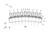
なお、第2グリッド14は平板状に形成され、平板状のままX線画像撮影システム10に搭載するが、X線源11から照射されるX線はコーンビーム状に広がるので、平板状のグリッドを用いると、グリッドの周縁部においてX線にケラレが発生することがある。ケラレを低減するためには、図12に示すように、第2グリッド14等をX線の広がりに合わせて円筒面状(あるいは球面状)に湾曲させることが好ましい。第2グリッド14は、金属層22とX線透過部27の密着性が良く、及び金属層22と支持基板23の接合は強固なので、このように湾曲させても破損し難い。
なお、第2グリッド14を例にしているが、線源グリッド12及びその製造方法は、上述の第2グリッド14及びその製造方法と同様である。その効果も同様である。
なお、線源グリッド12、第2グリッド14が吸収型グリッドであり、第1グリッド13が位相型グリッドであるが、第1グリッド13は吸収型グリッドであっても良い。第1グリッド13を吸収型グリッドにする場合、その構成や製造方法は前述と同様である。少なくとも線源グリッド12、第1グリッド13、第2グリッド14のうちいずれか1つに、前述の吸収型グリッドを使用していればその利益を得ることができる。
なお、本実施形態ではエッチング工程において、ボッシュプロセスによりシリコン基板41を深堀りして溝47を形成したが、他のエッチング方法で溝47を形成しても良い。例えば、シリコン単結晶の面方位によってエッチング速度が異なる異方性のウェットエッチングで溝47を形成しても良い。
また、被検体HをX線源と第1グリッドとの間に配置しているが、被検体Hを第1グリッドと第2グリッドとの間に配置してもよい。この場合にも同様に位相コントラスト画像が生成される。また、上記実施形態では、線源グリッドを設けているが、線源グリッドを省略してもよい。
本発明は、医療診断用の放射線画像撮影システムのほか、工業用や、非破壊検査等のその他の放射線撮影システムに適用可能である。また、本発明のグリッドは、X線撮影において散乱線を除去する散乱線除去用グリッドにも適用可能である。更に、本発明は、放射線として、X線以外にガンマ線等を用いる放射線画像撮影システムにも適用可能である。
Claims (14)
- 放射線を吸収する放射線吸収部と前記放射線を透過する放射線透過部が前記放射線の入射方向に対して垂直な方向に交互に配列されたグリッド層と、
少なくとも前記グリッド層側の面にイオン導電性材料を有し、前記グリッド層を支持する支持基板と、
前記グリッド層と前記支持基板の間に設けられ、前記グリッド層の前記放射線透過部に対しては成膜により密着され、前記支持基板に対しては陽極接合により接合された金属層と、を備え、
前記金属層は、第1薄膜と、第2薄膜または第3薄膜を含み、
第1薄膜は前記放射線吸収部を電気メッキにより形成するときにシーズ電極として機能する金属薄膜であり、
第2薄膜は、前記第1薄膜よりも前記放射線透過部に対する密着性が良く、前記第1薄膜と前記グリッド層の間に設けられる金属薄膜であり、
第3薄膜は前記陽極接合において前記第1薄膜よりも前記支持基板に対する接合性が良く、前記第1薄膜と前記支持基板の間に設けられる金属薄膜である放射線画像撮影用吸収型グリッド。 - 前記金属層は、前記第2薄膜、前記第1薄膜、前記第3薄膜の3層構造である請求の範囲第1項記載の放射線画像撮影用吸収型グリッド。
- 前記第1薄膜は、前記第2薄膜を介さずに前記放射線吸収部と直接接触している請求の範囲第1項記載の放射線画像撮影用吸収型グリッド
- 前記放射線透過部の表面に絶縁膜が形成されている請求の範囲第1項記載の放射線画像撮影用吸収型グリッド。
- 前記第2薄膜が、チタン、クロム、ニッケル、またはこれらのいずれかを含む合金である請求の範囲第1項記載の放射線画像撮影用吸収型グリッド。
- 前記第1薄膜が、金、白金、イリジウム、パラジウム、ロジウム、またはこれらのいずれかを含む合金である請求の範囲第1項記載の放射線画像撮影用吸収型グリッド。
- 前記第3薄膜が、アルミニウム、ニッケル、モリブデン、タングステン、またはこれらのいずれかを含む合金である請求の範囲第1項記載の放射線画像撮影用吸収型グリッド。
- 前記支持基板の熱膨張係数が前記放射線透過部の熱膨張係数よりも大きい場合に、
前記第1薄膜、前記第2薄膜及び前記第3薄膜の熱膨張係数は、前記支持基板の熱膨張係数以下でかつ前記放射線透過部の熱膨張係数以上である請求の範囲第2項記載の放射線画像撮影用吸収型グリッド。 - 前記支持基板は、イオン導電性基板である請求の範囲第1項記載の放射線画像撮影用吸収型グリッド。
- 前記支持基板は、前記放射線透過部と同じ材料で形成された基板と、この基板上に設けられたイオン導電性薄膜とからなり、前記イオン導電性薄膜によって前記金属層に接合している請求の範囲第1項記載の放射線画像撮影用吸収型グリッド。
- 放射線を透過する放射線透過部の材料からなるエッチング基板の一方の表面に、電気メッキ工程においてシーズ電極になる第1薄膜に加えて、前記第1薄膜の成膜前または成膜後に、前記シーズ電極よりも前記エッチング基板との密着性が良く、前記第1薄膜と前記エッチング基板の間に成膜される第2薄膜と、前記シーズ電極よりも支持基板との接合性が良く、前記第1薄膜上に成膜される第3薄膜のうち少なくとも一方を成膜し、少なくとも2種類の金属薄膜を有する金属層を形成する金属層形成工程と、
前記金属層に前記支持基板を接触させて陽極接合をすることにより、前記金属層が形成された前記エッチング基板と前記支持基板の接合体を形成する接合工程と、
前記接合体の前記エッチング基板を所定パターンにエッチングし、前記放射線を吸収する放射線吸収部になる溝と前記放射線透過部を形成し、前記溝の底部に前記金属層を露呈させるエッチング工程と、
前記溝に露呈された前記金属層をシーズ電極として、電気メッキにより前記溝に前記放射線を吸収する放射線吸収材を埋め込む電気メッキ工程と、
を備える放射線画像撮影用吸収型グリッドの製造方法。 - 前記金属層形成工程では、前記エッチング基板上に、前記第2薄膜と、前記第1薄膜と、前記第3薄膜をこの順に成膜し、3種の金属薄膜からなる前記金属層を形成する請求の範囲第11項記載の放射線画像撮影用吸収型グリッドの製造方法。
- 前記金属層形成工程では、前記複数の金属薄膜を全て同じ成膜装置で真空を破らずに成膜する請求の範囲第11項記載の放射線画像撮影用吸収型グリッドの製造方法。
- 放射線源から照射される放射線を、吸収型グリッドを介して撮影して位相コントラスト画像を生成する放射線画像撮影システムにおいて、
前記吸収型グリッドは、前記放射線を吸収する放射線吸収部と前記放射線を透過する放射線透過部が前記放射線の入射方向に対して垂直な方向に交互に配列されたグリッド層と、
少なくとも前記グリッド層側の面にイオン導電性材料を有し、前記グリッド層を支持する支持基板と、
前記グリッド層と前記支持基板の間に設けられ、前記グリッド層の前記放射線透過部に対しては成膜により密着され、前記支持基板に対しては陽極接合により接合された金属層とを有し、
前記金属層は、第1薄膜と、第2薄膜または第3薄膜を含み、
前記第1薄膜は前記放射線吸収部を電気メッキにより形成するときにシーズ電極として機能する金属薄膜であり、
前記第2薄膜は、前記第1薄膜よりも前記放射線透過部に対する密着性が良く、前記第1薄膜と前記グリッド層の間に設けられる金属薄膜であり、
前記第3薄膜は前記陽極接合において前記第1薄膜よりも前記支持基板に対する接合性が良く、前記第1薄膜と前記支持基板の間に設けられる金属薄膜である放射線画像撮影システム。
Applications Claiming Priority (2)
| Application Number | Priority Date | Filing Date | Title |
|---|---|---|---|
| JP2012-047256 | 2012-03-02 | ||
| JP2012047256A JP2013181916A (ja) | 2012-03-02 | 2012-03-02 | 放射線画像撮影用吸収型グリッド及びその製造方法、並びに放射線画像撮影システム |
Publications (1)
| Publication Number | Publication Date |
|---|---|
| WO2013129308A1 true WO2013129308A1 (ja) | 2013-09-06 |
Family
ID=49082506
Family Applications (1)
| Application Number | Title | Priority Date | Filing Date |
|---|---|---|---|
| PCT/JP2013/054750 Ceased WO2013129308A1 (ja) | 2012-03-02 | 2013-02-25 | 放射線画像撮影用吸収型グリッド及びその製造方法、並びに放射線画像撮影システム |
Country Status (2)
| Country | Link |
|---|---|
| JP (1) | JP2013181916A (ja) |
| WO (1) | WO2013129308A1 (ja) |
Cited By (1)
| Publication number | Priority date | Publication date | Assignee | Title |
|---|---|---|---|---|
| EP3826032A1 (en) * | 2019-11-22 | 2021-05-26 | Koninklijke Philips N.V. | Modular fabrication technique for gratings for interferometric x-ray imaging |
Families Citing this family (4)
| Publication number | Priority date | Publication date | Assignee | Title |
|---|---|---|---|---|
| JP2016221684A (ja) * | 2015-05-27 | 2016-12-28 | 大日本印刷株式会社 | 金属充填構造体及びその製造方法 |
| JP6856624B2 (ja) * | 2016-03-29 | 2021-04-07 | 株式会社東芝 | 中性子グリッド、中性子グリッド積層体、中性子グリッド装置、および中性子グリッドの製造方法 |
| KR101882141B1 (ko) | 2017-04-28 | 2018-08-24 | 한국광기술원 | 분광센서 및 이의 제조방법과 이를 이용한 분광장치 |
| JP7059545B2 (ja) * | 2017-09-20 | 2022-04-26 | 大日本印刷株式会社 | 構造体の製造方法、および構造体 |
Citations (5)
| Publication number | Priority date | Publication date | Assignee | Title |
|---|---|---|---|---|
| JP2011157622A (ja) * | 2010-01-08 | 2011-08-18 | Canon Inc | 微細構造体の製造方法 |
| WO2011122506A1 (en) * | 2010-03-30 | 2011-10-06 | Fujifilm Corporation | Grid for radiation imaging and method for producing the same |
| WO2012008120A1 (ja) * | 2010-07-15 | 2012-01-19 | コニカミノルタエムジー株式会社 | 金属格子の製造方法および金属格子 |
| WO2012008118A1 (ja) * | 2010-07-15 | 2012-01-19 | コニカミノルタエムジー株式会社 | 金属格子の製造方法および金属格子 |
| WO2012026223A1 (ja) * | 2010-08-25 | 2012-03-01 | 富士フイルム株式会社 | 放射線画像撮影用グリッド及びその製造方法、並びに放射線画像撮影システム |
-
2012
- 2012-03-02 JP JP2012047256A patent/JP2013181916A/ja active Pending
-
2013
- 2013-02-25 WO PCT/JP2013/054750 patent/WO2013129308A1/ja not_active Ceased
Patent Citations (5)
| Publication number | Priority date | Publication date | Assignee | Title |
|---|---|---|---|---|
| JP2011157622A (ja) * | 2010-01-08 | 2011-08-18 | Canon Inc | 微細構造体の製造方法 |
| WO2011122506A1 (en) * | 2010-03-30 | 2011-10-06 | Fujifilm Corporation | Grid for radiation imaging and method for producing the same |
| WO2012008120A1 (ja) * | 2010-07-15 | 2012-01-19 | コニカミノルタエムジー株式会社 | 金属格子の製造方法および金属格子 |
| WO2012008118A1 (ja) * | 2010-07-15 | 2012-01-19 | コニカミノルタエムジー株式会社 | 金属格子の製造方法および金属格子 |
| WO2012026223A1 (ja) * | 2010-08-25 | 2012-03-01 | 富士フイルム株式会社 | 放射線画像撮影用グリッド及びその製造方法、並びに放射線画像撮影システム |
Cited By (4)
| Publication number | Priority date | Publication date | Assignee | Title |
|---|---|---|---|---|
| EP3826032A1 (en) * | 2019-11-22 | 2021-05-26 | Koninklijke Philips N.V. | Modular fabrication technique for gratings for interferometric x-ray imaging |
| WO2021099274A1 (en) * | 2019-11-22 | 2021-05-27 | Koninklijke Philips N.V. | Modular fabrication technique for gratings for interferometric x-ray imaging |
| CN114730644A (zh) * | 2019-11-22 | 2022-07-08 | 皇家飞利浦有限公司 | 用于干涉式x射线成像的光栅的模块化制造技术 |
| CN114730644B (zh) * | 2019-11-22 | 2025-09-23 | 皇家飞利浦有限公司 | 用于干涉式x射线成像的光栅的模块化制造技术 |
Also Published As
| Publication number | Publication date |
|---|---|
| JP2013181916A (ja) | 2013-09-12 |
Similar Documents
| Publication | Publication Date | Title |
|---|---|---|
| JP5660910B2 (ja) | 放射線画像撮影用グリッドの製造方法 | |
| JP6253233B2 (ja) | 透過型x線ターゲットおよび、該透過型x線ターゲットを備えた放射線発生管、並びに、該放射線発生管を備えた放射線発生装置、並びに、該放射線発生装置を備えた放射線撮影装置 | |
| WO2013129308A1 (ja) | 放射線画像撮影用吸収型グリッド及びその製造方法、並びに放射線画像撮影システム | |
| JP6207246B2 (ja) | 透過型ターゲットおよび該透過型ターゲットを備える放射線発生管、放射線発生装置、及び、放射線撮影装置 | |
| JP5581321B2 (ja) | X線ct装置 | |
| EP3136970B1 (en) | X-ray interferometric imaging system | |
| JP6338341B2 (ja) | 透過型放射線管、放射線発生装置及び放射線撮影システム | |
| JP5977489B2 (ja) | 散乱防止x線グリッド装置の製造方法 | |
| EP2273286A2 (en) | Radiation image detection apparatus and manufacturing method of the same | |
| JP6697391B2 (ja) | 一体型の患者テーブルデジタルx線線量計のための方法およびシステム | |
| CN101413905A (zh) | X射线微分干涉相衬成像系统 | |
| JP2014067513A (ja) | 放射線発生ターゲット、放射線発生ユニット及び放射線撮影システム | |
| JP2015092953A (ja) | 放射線撮影装置及び放射線撮影システム | |
| EP2770805A2 (en) | X-ray imaging system including flat panel type X-ray generator, X-ray generator, and electron emission device | |
| WO2013129309A1 (ja) | 放射線画像撮影用吸収型グリッド及びその製造方法、並びに放射線画像撮影システム | |
| JP2012149982A (ja) | 放射線画像撮影用格子ユニット及び放射線画像撮影システム、並びに格子体の製造方法 | |
| JP2012132793A (ja) | 放射線画像撮影用グリッド及びその製造方法、並びに放射線画像撮影システム | |
| WO2012053342A1 (ja) | 放射線画像撮影用グリッド及びその製造方法、並びに放射線画像撮影システム | |
| JP2012249847A (ja) | 放射線画像撮影用グリッド及びその製造方法、並びに放射線画像撮影システム | |
| CN114047540B (zh) | 一种强流脉冲电子束束流密度分布的测量方法及测量系统 | |
| JP2014003988A (ja) | 放射線画像撮影用グリッド及びその製造方法、並びに放射線画像撮影システム | |
| JP2013188286A (ja) | 放射線画像撮影用グリッド及びその製造方法、並びに放射線画像撮影システム | |
| CN109646027A (zh) | 乳腺成像系统及其光路装置 | |
| CN120677537A (zh) | 用于选择性透射电磁辐射的微结构 | |
| JP2020061484A (ja) | 放射線撮像装置及びその製造方法、並びに、放射線撮像システム |
Legal Events
| Date | Code | Title | Description |
|---|---|---|---|
| 121 | Ep: the epo has been informed by wipo that ep was designated in this application |
Ref document number: 13754858 Country of ref document: EP Kind code of ref document: A1 |
|
| NENP | Non-entry into the national phase |
Ref country code: DE |
|
| 122 | Ep: pct application non-entry in european phase |
Ref document number: 13754858 Country of ref document: EP Kind code of ref document: A1 |