WO2013129160A1 - 光学表示パネルの製造方法および光学表示パネルの製造システム - Google Patents
光学表示パネルの製造方法および光学表示パネルの製造システム Download PDFInfo
- Publication number
- WO2013129160A1 WO2013129160A1 PCT/JP2013/053860 JP2013053860W WO2013129160A1 WO 2013129160 A1 WO2013129160 A1 WO 2013129160A1 JP 2013053860 W JP2013053860 W JP 2013053860W WO 2013129160 A1 WO2013129160 A1 WO 2013129160A1
- Authority
- WO
- WIPO (PCT)
- Prior art keywords
- optical
- optical cell
- film
- cell
- sheet piece
- Prior art date
Links
Images


Classifications
-
- B—PERFORMING OPERATIONS; TRANSPORTING
- B32—LAYERED PRODUCTS
- B32B—LAYERED PRODUCTS, i.e. PRODUCTS BUILT-UP OF STRATA OF FLAT OR NON-FLAT, e.g. CELLULAR OR HONEYCOMB, FORM
- B32B38/00—Ancillary operations in connection with laminating processes
- B32B38/18—Handling of layers or the laminate
-
- B—PERFORMING OPERATIONS; TRANSPORTING
- B32—LAYERED PRODUCTS
- B32B—LAYERED PRODUCTS, i.e. PRODUCTS BUILT-UP OF STRATA OF FLAT OR NON-FLAT, e.g. CELLULAR OR HONEYCOMB, FORM
- B32B37/00—Methods or apparatus for laminating, e.g. by curing or by ultrasonic bonding
- B32B37/12—Methods or apparatus for laminating, e.g. by curing or by ultrasonic bonding characterised by using adhesives
-
- B—PERFORMING OPERATIONS; TRANSPORTING
- B32—LAYERED PRODUCTS
- B32B—LAYERED PRODUCTS, i.e. PRODUCTS BUILT-UP OF STRATA OF FLAT OR NON-FLAT, e.g. CELLULAR OR HONEYCOMB, FORM
- B32B37/00—Methods or apparatus for laminating, e.g. by curing or by ultrasonic bonding
- B32B37/14—Methods or apparatus for laminating, e.g. by curing or by ultrasonic bonding characterised by the properties of the layers
- B32B37/16—Methods or apparatus for laminating, e.g. by curing or by ultrasonic bonding characterised by the properties of the layers with all layers existing as coherent layers before laminating
- B32B37/22—Methods or apparatus for laminating, e.g. by curing or by ultrasonic bonding characterised by the properties of the layers with all layers existing as coherent layers before laminating involving the assembly of both discrete and continuous layers
-
- B—PERFORMING OPERATIONS; TRANSPORTING
- B32—LAYERED PRODUCTS
- B32B—LAYERED PRODUCTS, i.e. PRODUCTS BUILT-UP OF STRATA OF FLAT OR NON-FLAT, e.g. CELLULAR OR HONEYCOMB, FORM
- B32B38/00—Ancillary operations in connection with laminating processes
- B32B38/18—Handling of layers or the laminate
- B32B38/1866—Handling of layers or the laminate conforming the layers or laminate to a convex or concave profile
-
- G—PHYSICS
- G02—OPTICS
- G02F—OPTICAL DEVICES OR ARRANGEMENTS FOR THE CONTROL OF LIGHT BY MODIFICATION OF THE OPTICAL PROPERTIES OF THE MEDIA OF THE ELEMENTS INVOLVED THEREIN; NON-LINEAR OPTICS; FREQUENCY-CHANGING OF LIGHT; OPTICAL LOGIC ELEMENTS; OPTICAL ANALOGUE/DIGITAL CONVERTERS
- G02F1/00—Devices or arrangements for the control of the intensity, colour, phase, polarisation or direction of light arriving from an independent light source, e.g. switching, gating or modulating; Non-linear optics
- G02F1/01—Devices or arrangements for the control of the intensity, colour, phase, polarisation or direction of light arriving from an independent light source, e.g. switching, gating or modulating; Non-linear optics for the control of the intensity, phase, polarisation or colour
- G02F1/13—Devices or arrangements for the control of the intensity, colour, phase, polarisation or direction of light arriving from an independent light source, e.g. switching, gating or modulating; Non-linear optics for the control of the intensity, phase, polarisation or colour based on liquid crystals, e.g. single liquid crystal display cells
- G02F1/133—Constructional arrangements; Operation of liquid crystal cells; Circuit arrangements
- G02F1/1333—Constructional arrangements; Manufacturing methods
-
- B—PERFORMING OPERATIONS; TRANSPORTING
- B32—LAYERED PRODUCTS
- B32B—LAYERED PRODUCTS, i.e. PRODUCTS BUILT-UP OF STRATA OF FLAT OR NON-FLAT, e.g. CELLULAR OR HONEYCOMB, FORM
- B32B2307/00—Properties of the layers or laminate
- B32B2307/40—Properties of the layers or laminate having particular optical properties
- B32B2307/42—Polarizing, birefringent, filtering
-
- B—PERFORMING OPERATIONS; TRANSPORTING
- B32—LAYERED PRODUCTS
- B32B—LAYERED PRODUCTS, i.e. PRODUCTS BUILT-UP OF STRATA OF FLAT OR NON-FLAT, e.g. CELLULAR OR HONEYCOMB, FORM
- B32B2329/00—Polyvinylalcohols, polyvinylethers, polyvinylaldehydes, polyvinylketones or polyvinylketals
- B32B2329/04—Polyvinylalcohol
-
- B—PERFORMING OPERATIONS; TRANSPORTING
- B32—LAYERED PRODUCTS
- B32B—LAYERED PRODUCTS, i.e. PRODUCTS BUILT-UP OF STRATA OF FLAT OR NON-FLAT, e.g. CELLULAR OR HONEYCOMB, FORM
- B32B2457/00—Electrical equipment
- B32B2457/20—Displays, e.g. liquid crystal displays, plasma displays
-
- B—PERFORMING OPERATIONS; TRANSPORTING
- B32—LAYERED PRODUCTS
- B32B—LAYERED PRODUCTS, i.e. PRODUCTS BUILT-UP OF STRATA OF FLAT OR NON-FLAT, e.g. CELLULAR OR HONEYCOMB, FORM
- B32B2551/00—Optical elements
-
- Y—GENERAL TAGGING OF NEW TECHNOLOGICAL DEVELOPMENTS; GENERAL TAGGING OF CROSS-SECTIONAL TECHNOLOGIES SPANNING OVER SEVERAL SECTIONS OF THE IPC; TECHNICAL SUBJECTS COVERED BY FORMER USPC CROSS-REFERENCE ART COLLECTIONS [XRACs] AND DIGESTS
- Y10—TECHNICAL SUBJECTS COVERED BY FORMER USPC
- Y10T—TECHNICAL SUBJECTS COVERED BY FORMER US CLASSIFICATION
- Y10T156/00—Adhesive bonding and miscellaneous chemical manufacture
- Y10T156/10—Methods of surface bonding and/or assembly therefor
- Y10T156/1002—Methods of surface bonding and/or assembly therefor with permanent bending or reshaping or surface deformation of self sustaining lamina
- Y10T156/1043—Subsequent to assembly
- Y10T156/1044—Subsequent to assembly of parallel stacked sheets only
- Y10T156/1048—Subsequent to assembly of parallel stacked sheets only to form dished or receptacle-like product
Definitions
- the present invention conveys the carrier film from a continuous roll formed by winding a long carrier film on which an optical film having a predetermined film width including an adhesive is laminated, and the optical film being peeled from the carrier film
- the present invention relates to an optical display panel manufacturing method and an optical display panel manufacturing system in which the peeled optical film is attached to an optical cell via the adhesive.
- An optical display panel is formed by feeding a carrier film from a continuous roll of a long carrier film on which a polarizing film is laminated, peeling the polarizing film from the carrier film, and attaching the polarizing film to the first cell surface and the second cell surface of the optical cell, respectively.
- manufacture (refer patent document 1).
- an optical cell (optical display panel) to which an optical cell and a polarizing film are attached is arranged by rotating a large number of cylindrical transport rollers (transport rollers) so as to rotate in the transport direction of the optical cell. ).
- transport rollers transport rollers
- the optical cell is transported by the transport roller, thereby reducing the contact between the transport roller and the optical cell surface.
- a surface contact conveyance means such as a belt conveyor, dust and dirt adhering to the conveyor transfer to the optical cell affixing surface and cause display defects. It has become.
- Patent Document 2 In addition, in order to make direct contact between the optical cell surface and the transport roller in a short time, it has been proposed to attach a polarizing film first from the surface of the optical cell in contact with the transport roller (Patent Document 2). reference).
- JP 2005-37417 A Japanese Patent No. 4588783
- optical cells have been reduced in size and thickness.
- the optical cell is conveyed by the tension of the polarizing film at the time of application.
- the optical cell may warp upward (curve in a convex shape) (see FIGS. 4A and 4B). Due to this warping phenomenon, the end of the optical cell (front end and rear end) falls between adjacent transport rollers, and the end of the optical cell contacts the transport roller (the end of the optical cell is the transport roller surface). (See FIG. 5). This contact causes a crack or a chip at the end of the optical cell, and when attached to the optical cell, the attachment yield (productivity) is reduced.
- the present invention has been made in view of the above situation, and by attaching an optical film from the lower surface of the optical cell, the optical cell has warped its central portion upward in a side view in the transport direction (convex shape). Even if the optical cell is rotated 90 ° after the optical film is attached, the end of the optical cell is prevented from falling into the gap between the adjacent transport rollers, thereby preventing cracks and chipping.
- An optical display panel manufacturing method and an optical display panel manufacturing system are provided.
- the present invention is a method of manufacturing an optical display panel, A transporting step of transporting an optical cell having a thickness of 0.2 mm to 1.0 mm with a transporting roller unit disposed so as to be orthogonal to the transporting direction of the optical cell; A sheet piece of the optical film being conveyed from a continuous roll formed by winding a long carrier film on which an optical film having a predetermined film width containing an adhesive is wound, and being peeled from the carrier film, or A pasting step of pasting the peeled sheet piece of the optical film to the lower surface of the optical cell on the side in contact with the transport roller part via the adhesive, A rotating step of rotating the optical cell having the sheet piece formed on the lower surface by being attached in the attaching step by 90 ° with respect to the transport direction of the optical cell.
- the optical cell is rotated by 90 ° with respect to the transport direction, so that the optical cell is positioned above the center in the side view in the transport direction.
- the optical cell is changed to a state in which the optical cell is warped upward (curved in a convex shape) in a front view with respect to the transport direction. Accordingly, the optical cell end can be prevented from falling into the gap between adjacent transport rollers, the optical cell can be stably transported, and cracks and chipping of the optical cell end can be prevented.
- 90 ° rotated state means that the long side of the optical cell after rotation (or rotation) is parallel to the short side before rotation (or rotation), and the optical cell after rotation (or rotation) This means that the short side is parallel to the long side before rotation (or turning).
- Swivel means that the optical cell is turned upside down and rotated 90 °.
- the number of times the optical cell end falls into the gap between the transport rollers is preferably small, for example, preferably 3 times or less, and more preferably 1 time or less. It is preferable to shorten the distance from the sticking step to the rotating step and reduce the number of rollers arranged.
- the lower or upper surface of the optical cell that is transported after the pasting step is transported by the negative pressure suction plate part, and the negative pressure suction plate part is rotated by 90 °, whereby the optical cell is rotated by 90 ° with respect to the transport direction. You may make it.
- the arrangement of the conveyance roller unit so as to be orthogonal to the conveyance direction of the optical cell includes substantially orthogonal or substantially orthogonal, and the optical cell is conveyed by the rotation of the roller of the conveyance roller unit. An arrangement that only needs to be transported in the direction.
- the state in which the optical cell is warped upward means that both end portions (end portions of opposite sides) or one of the end portions warps downward (floor side). including.
- the thickness of the optical cell is 0.2 mm to 1.0 mm. This is because, as the thickness of the optical cell becomes smaller than 1.0 mm as described above, the optical cell is more likely to be warped (curved) due to the tension when the optical film is applied. Further, if the thickness of the optical cell is smaller than 0.2 mm, the warping state becomes too large and the display characteristics of the optical cell are remarkably deteriorated. However, it is difficult to commercialize the optical cell.
- the optical cell surface is rectangular
- the transport step transports the optical cell with the transport roller unit so that the short side of the optical cell coincides with the transport direction of the optical cell
- the sheet piece is attached to the lower surface of the optical cell via the adhesive.
- the short side (length in the short direction) of the optical cell is shorter than the long side (length in the longitudinal direction)
- the influence of the warped state after application is large, and the end of the optical cell is adjacent. It becomes easy to fall into the gap between the matching transport rollers. Therefore, when the short side of the optical cell is coincident with the transport direction of the optical cell, the effect of the present invention is exhibited more than when the long side is coincident with the transport direction.
- the length of the short side of the optical cell is 100 mm to 230 mm, and the length of the long side of the optical cell is 170 mm to 340 mm.
- the smaller the optical cell the easier it is for the end of the optical cell to fall into the gap between adjacent transport rollers due to the influence of the warped state after application. Therefore, in the case of a small optical cell, the effect of the present invention is exhibited more than in the case of an optical cell having a larger size.
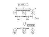
- the relationship between the length (L) of the side that coincides with the transport direction of the optical cell and the distance (D) between adjacent roller shafts of the transport roller portion is 0.5> D / L.
- the optical cell is transported by the transport roller section between the pasting process and the rotating process.
- the relational expression 0.5> D / L the end of the optical cell does not fall into the gap between the transport rollers, and the generation of cracks and chips can be further prevented.
- the relational expression is more preferably 0.3> D / L.
- the end of the optical cell falls into the gap between the transport rollers, and cracks and chips are likely to occur.
- the optical in which the sheet piece (1st sheet piece) of the said optical film (1st optical film) is not formed is conveyed from a second continuous roll formed by winding a long second carrier film in which a second optical film having a predetermined film width including an adhesive is laminated on the surface of the cell, 2 It has further the 2nd sticking process which sticks the 2nd sheet piece of this 2nd optical film currently peeled from the carrier film, or the 2nd sheet piece of this 2nd optical film peeled through this adhesive.
- the second sheet piece of the second optical film may be pasted on the upper surface of the optical cell (the surface not in contact with the transport roller).
- the optical cell is further turned upside down, and the second sticking step is arranged on the lower surface of the optical cell (the surface on the side in contact with the transport roller). You may affix the 2nd sheet piece of a film.
- the present method may include a turning step having the rotation step and the inversion step, and the rotation process and the inversion process may be performed simultaneously.
- the third sheet piece of the third optical film is laminated so as to be laminated on the first sheet piece or the second sheet piece after the second attaching step. You may further have a sticking process.
- Another aspect of the present invention is an optical display panel manufacturing system, A transport roller unit disposed so as to be orthogonal to the transport direction of the optical cell and transporting an optical cell having a thickness of 0.2 mm to 1.0 mm; A sheet piece of the optical film being conveyed from a continuous roll formed by winding a long carrier film on which an optical film having a predetermined film width containing an adhesive is wound, and being peeled from the carrier film, or Affixing part for attaching the peeled sheet piece of the optical film to the lower surface of the optical cell on the side in contact with the transport roller part via the adhesive, And a rotating unit that rotates the optical cell, on which the sheet piece is formed on the lower surface by being pasted by the pasting unit, by 90 ° with respect to the transport direction of the optical cell.
- the optical cell is rotated by 90 ° with respect to the transport direction, so that the optical cell is positioned above the center in the side view in the transport direction.
- the optical cell is changed to a state in which the optical cell is warped upward (curved in a convex shape) in a front view with respect to the transport direction. Accordingly, the optical cell end can be prevented from falling into the gap between adjacent transport rollers, the optical cell can be stably transported, and cracks and chipping of the optical cell end can be prevented.
- the number of times the optical cell end falls into the gap between the transport rollers is preferably 3 times or less, more preferably 1 time or less, and particularly preferably zero. It is preferable to shorten the distance from the sticking part to the rotating part and reduce the number of rollers arranged.
- the lower or upper surface of the optical cell conveyed from the pasting part is conveyed by the negative pressure adsorption plate part, and the negative pressure adsorption plate part is rotated by 90 °, so that the optical cell is rotated by 90 ° with respect to the conveyance direction. You may make it.
- the optical cell surface is rectangular
- the transport roller unit transports the optical cell such that the short side of the optical cell coincides with the transport direction of the optical cell;
- the sticking part sticks the sheet piece to the lower surface of the optical cell via the adhesive.
- the short side length of the optical cell is 100 mm or more and 230 mm or less
- the length of the long side of the optical cell is 170 mm or more and 340 mm or less.
- the relationship between the length (L) of the first side coinciding with the transport direction of the optical cell and the distance (D) between adjacent roller shafts of the transport roller portion is 0.5> D / L.
- the sheet piece (1st sheet piece) of the said optical film (1st optical film) is not formed after the process of the said sticking part (1st sticking part) and a rotation part.
- the second carrier film is conveyed from a second continuous roll formed by winding a long second carrier film in which a second optical film having a predetermined film width including an adhesive is laminated on the surface of the optical cell, A second pasting portion for pasting the second sheet piece of the second optical film being peeled off from the second carrier film or the second sheet piece of the second optical film being peeled off via the adhesive.
- a 2nd sticking part may stick the 2nd sheet piece of a 2nd optical film on the upper surface (surface which is not in contact with a conveyance roller) of an optical cell.
- it further includes a reversing part that vertically inverts the optical cell, and the second attaching part is provided on the lower surface of the optical cell (the surface in contact with the transport roller) on the second surface. You may affix the 2nd sheet piece of 2 optical films.
- the said rotation part and inversion part may be comprised by the turning part which performs rotation and inversion simultaneously.
- the apparatus further includes a third pasting portion that is pasted so as to be laminated on the first sheet piece or the second sheet piece after the pasting process of the second pasting portion.
- the first sticking unit is opposite to the sticking roller that presses the first sheet piece of the first optical film against the optical cell surface on the side in contact with the conveying roller part.
- a receiving roller that is arranged in the form of a roller, and is in contact with the conveying roller unit while conveying the first sheet piece of the first optical film and the optical cell between the sticking roller and the receiving roller.
- a first sheet piece is attached to the optical cell surface.
- the second sticking portion faces the sticking roller, the sticking roller that presses the second sheet piece of the second optical film against the optical cell surface on the side not in contact with the transport roller portion, and the sticking roller.
- a second sheet piece is attached to the cell surface.
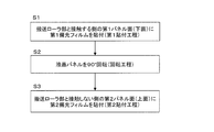
- FIG. 3 is a flowchart of a method for manufacturing the optical display panel of Embodiment 1.
- FIG. 3 is a diagram for explaining the optical display panel manufacturing system according to the first embodiment.
- the figure for demonstrating a relational expression (0.5> D / L).
- the optical film only needs to include an adhesive layer as the outermost layer, and may have a single layer structure or a multilayer structure.
- the optical film is, for example, a plastic film, and the film thickness is about 5 ⁇ m to 200 ⁇ m.
- examples of the optical film include a polarizer and a polarizing film
- the polarizing film has a structure in which a polarizer protective film is laminated on one or both sides of the polarizer.
- a surface protective film for protecting the polarizer or the polarizing film from scratches during transportation is laminated.
- examples of other optical films include optical compensation films such as retardation films and brightness enhancement films.
- a retardation film and / or a brightness enhancement film may be laminated on a polarizer or a polarizing film.
- the polarizer has an absorption axis in the stretching direction, and an absorption axis in the longitudinal direction of the long polarizing film (or a transmission axis in the short direction (film width direction) of the long polarizing film).
- a film having an absorption axis is referred to as an “MD polarizing film”, and a film having an absorption axis in the short direction (film width direction) of a long polarizing film may be referred to as a “TD polarizing film”.
- the polarizing film examples include a two-color polarizing film.
- the two-color polarizing film includes (A) a step of drying a polyvinyl alcohol-based film that has been dyed, crosslinked and stretched to obtain a polarizer, and (B) a protective layer (polarizer protective film) on one or both sides of the polarizer. ), And (C) a step of heat treatment after bonding.
- Each treatment of dyeing, crosslinking and stretching of the polyvinyl alcohol film need not be performed separately and may be performed simultaneously, and the order of the treatments may be arbitrary.
- a polyvinyl alcohol film is immersed in a solution containing iodine or a dichroic dye, dyed by adsorbing iodine or a dichroic dye, washed, and stretched in a solution containing boric acid or borax. After uniaxial stretching at a magnification of 3 to 7 times, it is dried.
- the brightness enhancement film examples include a reflective polarizing film having a multilayer structure having a reflection axis and a transmission axis.
- the reflective polarizing film can be obtained, for example, by alternately laminating and stretching a plurality of polymer films A and B of two different materials.
- the refractive index of only material A increases and changes in the stretching direction, birefringence is developed, and the stretching direction having a difference in refractive index at the interface of material AB becomes the reflection axis, and the direction in which no refractive index difference occurs (non-stretching direction). It becomes the transmission axis.
- This reflective polarizing film has a transmission axis in its longitudinal direction and an absorption axis in its short direction (film width direction).
- the pressure-sensitive adhesive in the pressure-sensitive adhesive layer contained in the outermost layer of the optical film is not particularly limited, and examples thereof include acrylic pressure-sensitive adhesives, silicone-based pressure-sensitive adhesives, and urethane-based pressure-sensitive adhesives.
- the carrier film for example, a film such as a plastic film (for example, a polyethylene terephthalate film, a polyolefin film, etc.) can be used. Further, if necessary, an appropriate material such as a silicone-based, long-chain alkyl-based, fluorine-based or molybdenum sulfide-coated material may be used. *
- the form in which the optical film is formed on the carrier film is not particularly limited.
- a continuous roll what wound the optical film laminated body which has (1) carrier film and the optical film containing the adhesive formed on the said carrier film in roll shape is mentioned, for example.
- the optical display panel manufacturing system leaves the carrier film uncut and keeps the optical film (including the adhesive) at a predetermined cutting interval. It has a cutting means for cutting (half cut). In this cutting, for example, based on the inspection result of the defect inspection apparatus in the manufacturing system, the cutting may be performed so as to distinguish the non-defective sheet piece from the defective sheet piece.
- a continuous roll for example, (2) a roll of an optical film laminate having a carrier film and a sheet piece of an optical film containing an adhesive formed on the carrier film (so-called notched optics) Continuous roll of film).
- the optical display panel is one in which at least a polarizing film sheet piece is formed on one or both sides of an optical cell, and a drive circuit is incorporated as necessary.
- the optical cell include a liquid crystal cell and an organic EL cell.
- the liquid crystal cell for example, an arbitrary type such as a vertical alignment (VA) type or an in-plane switching (IPS) type can be used.
- VA vertical alignment
- IPS in-plane switching
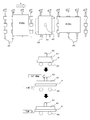
- the liquid crystal cell P shown in FIG. 2 has a configuration in which a liquid crystal layer is sealed between a pair of substrates (a first substrate Pa and a second substrate Pb) arranged to face each other.
- the thickness of the optical cell is 0.2 mm to 1.0 mm.
- FIG. 1 is a flowchart illustrating the manufacturing method according to the first embodiment.
- the second sheet piece of the second polarizing film is adhered to the second cell surface (upper surface) of the optical cell in which the first sheet piece of the first polarizing film is not formed. It further has the 2nd sticking process stuck via an agent.
- the first polarizing film laminate laminated film in which the polarizing film is laminated on the carrier film
- the first polarizing film is fed out and transported downstream from the first continuous roll.
- the first polarizing film is cut at a predetermined cutting interval in the film width direction orthogonal to the longitudinal direction while leaving the first carrier film, and the first sheet piece of the first polarizing film is formed on the carrier film.
- disconnection is unnecessary.
- the first carrier film is turned inside and folded at the tip of the peeling portion to peel the first sheet piece of the first polarizing film from the first carrier film and supplied to the sticking position of the first sticking portion.
- the optical cell is transported by the transport roller unit to a position where the first paste unit is pasted in a state where the first cell surface (lower surface) is in contact with the transport roller unit (in a state of facing the floor surface) ( Transport process).
- the first sticking unit includes a sticking roller that presses the first sheet piece of the first optical film against the first cell surface (lower surface), and a receiving roller that is disposed to face the sticking roller.
- step S1 while conveying the first sheet piece of the first optical film and the optical cell between the sticking roller and the receiving roller, the first cell surface (lower surface) of the optical cell facing the floor surface is conveyed. Then, the first sheet piece of the first polarizing film having the absorption axis in the film longitudinal direction is pasted (step S1).
- the second polarizing film laminate (a laminated film in which the second polarizing film is laminated on the second carrier film) is fed out and conveyed downstream from the second continuous roll.
- the second polarizing film is cut at a predetermined cutting interval in the film width direction orthogonal to the longitudinal direction while leaving the second carrier film, and the second sheet piece of the second polarizing film is formed on the second carrier film.
- the second carrier film is turned inside and folded at the tip of the peeling portion to peel the second sheet piece of the second polarizing film from the second carrier film and supplied to the sticking position of the second sticking portion.
- the optical cell has the first cell surface (the state where the first polarizing film is adhered) in contact with the conveyance roller unit (in the state facing the floor surface) by the conveyance roller unit.
- the second sticking portion has a sticking roller that presses the second sheet piece of the second optical film against the second cell surface (upper surface), and a receiving roller that is disposed to face the sticking roller.
- the absorption axis extends in the film longitudinal direction on the second cell surface (upper surface) of the optical cell.
- the 2nd sheet piece of the 2nd polarizing film which has is stuck (Step S3).
- An optical display panel manufacturing system is an optical display panel manufacturing system, A transport roller unit disposed so as to be orthogonal to the transport direction of the optical cell, and transporting the optical cell;
- the first carrier film is transported from a first continuous roll formed by winding a long first carrier film on which a first polarizing film having a predetermined film width including an adhesive is laminated, and is peeled from the first carrier film.
- the first sheet piece of the first polarizing film being peeled or the peeled first sheet piece of the first polarizing film is placed on the first cell surface (lower surface) of the optical cell on the side in contact with the transport roller unit.
- a first pasting part to be pasted through the adhesive A rotating unit that rotates the optical cell in which the first sheet piece is formed on the first cell surface (lower surface) by being rotated by 90 ° with respect to the transport direction of the optical cell by being bonded by the first bonding unit. And having.
- the 2nd cell surface (upper surface) of the optical cell in which the 1st sheet piece of a 1st polarizing film is not formed is the 1st of the predetermined film width containing an adhesive.
- the second sheet of the second polarizing film being transported from the second continuous roll formed by winding the long second carrier film on which the two polarizing films are laminated and being peeled from the second carrier film. It has further the 2nd sticking part which sticks the 2nd sheet piece of the 2nd polarizing film which peeled or peeled through the adhesive.
- This manufacturing system includes a plurality of sheet piece laminating apparatuses each having a carrier film transport unit, a peeling unit, and a pasting unit.
- stacking apparatus 100 laminates
- the second sheet piece laminating apparatus 200 the second sheet piece of the second polarizing film is attached to a second cell surface (upper surface) different from the first cell surface of the optical cell along the long side direction (parallel). Laminate with.
- the first sheet piece laminating apparatus 100 includes a carrier film transport unit 110, a transport roller unit 90 for transporting an optical cell, a peeling unit 104, and a first pasting unit 106.
- the second sheet piece laminating apparatus 200 includes a carrier film transport unit 210, a transport roller unit 90 for transporting the optical cell, a peeling unit 204, and a second pasting unit 206.
- the transport roller unit 90 transports the optical cell P up to the first pasting unit 106 so that the short side direction of the optical cell P and the panel transport direction A are parallel to each other.
- the sheet piece 111 of the 1st polarizing film 11 is affixed on the 1st cell surface Pa (lower surface side in FIG. 2) of the optical cell P by the affixing direction along the short side direction.
- the optical cell P to which the sheet piece 111 is attached is rotated 90 ° by the rotating unit 80. Therefore, after this rotation, the transport roller unit 90 transports the optical cell P to the second sticking unit 206 so that the long side direction of the optical cell P and the panel transport direction A are parallel to each other.
- the end of the optical cell P is changed to a state in which the front surface of the transport direction A warps in a convex shape (perpendicular to the transport direction A). Is prevented from falling into a gap between adjacent conveyance rollers (901, 902, 903). As shown in FIG. 6, the end of the optical cell P is transported so as not to fall into the gap between the adjacent transport rollers (901, 902, 903), so that the end is not cracked or chipped.
- the optical cell P can be stably conveyed.
- the optical cell is rectangular, and the transport roller unit 90 transports the optical cell P so that the short side (short-side length) of the optical cell P coincides with the transport direction A of the optical cell P. is there. Further, the present invention is suitable when the length of the short side of the optical cell P is 100 mm or more and 230 mm or less, and the length of the long side of the optical cell P is 170 mm or more and 340 mm or less.
- the distance (D) between adjacent roller shafts is preferably smaller than 1 ⁇ 2 of the length of the short side (100 mm or more and 230 mm or less), and more preferably less than 3. 1/5 is more preferable.
- the relationship between the length (L) of the first side that coincides with the conveyance direction A of the optical cell P and the distance (D) between adjacent roller axes of the conveyance roller unit 90 is 0. 5> D / L.
- FIG. 4A is an explanatory diagram for establishing this relationship.
- FIG. 4B shows a relationship 0.5 ⁇ D / L in which this relationship is not established. In the case of FIG. 4B, as shown in FIG. 5, the end of the optical cell falls into the gap between the transport rollers.
- the second sheet piece 211 of the second polarizing film 21 is attached to the second cell surface Pb (the upper surface side in FIG. 2) of the optical cell P in the attaching direction along the long side direction.
- the transport roller unit 90 transports the optical cell P in the transport direction A to the first sticking unit 106.
- the conveyance roller unit 90 includes a plurality of conveyance rollers. The transport roller is rotated to transport the optical cell P to the downstream side of the production line.
- the carrier film transport unit 110 has a long first carrier film 12 in which a long first polarizing film 11 (film part 11a and pressure-sensitive adhesive layer 11b) containing a pressure-sensitive adhesive is laminated from the first continuous roll 1.
- the first polarizing film laminate 10 is drawn out, the first polarizing film 11 is cut at a predetermined cutting interval, leaving the first carrier film 12, and the first sheet piece 111 of the first polarizing film 11 is cut into the first carrier film. 12 is formed.
- the first polarizing film 11 has an absorption axis in the film longitudinal direction.
- the carrier film conveyance unit 110 includes a cutting unit 101, a conveyance roller 114, a dancer roll 113, and a winding unit 115. Note that FIG. 2 is a schematic diagram, and the number and the installation position of the transport rollers 114 are not limited thereto.
- the cutting unit 101 fixes the first carrier film 12 by the adsorption unit 102, cuts the first polarizing film 11 at a predetermined interval, leaving the first carrier film 12, and the first carrier film 12 has a first portion on the first carrier film 12.
- a first sheet piece 111 of the polarizing film 11 is formed.
- Examples of the cutting unit 101 include a cutter and a laser device.
- the dancer roll 113 has a function of maintaining the tension of the first carrier film 12.
- the carrier film transport unit 110 transports the carrier film 12 via the dancer roll 113.
- the winding unit 105 winds up the first carrier film 12 from which the first sheet piece 111 has been peeled off. Moreover, it is not restrict
- a downstream feed roller, a transport roller may be further provided between the peeling unit 104 and the winding unit 105, and the first carrier film 12 may be transported by the downstream feed roller.
- an upstream feed roller (not shown) may be provided on the upstream side of conveyance from the peeling unit 104, and the first carrier film 12 may be conveyed by the upstream feed roller. Further, the upstream feed roller, the downstream feed roller, and the winding unit 105 may be linked to each other, or each may carry the first carrier film 12 alone.
- the peeling part 104 is folded back with the first carrier film 12 inside at the tip, peels off the first sheet piece 111 (including the adhesive) of the first polarizing film 11 from the first carrier film 12, and the first sticking To the pasting position of the unit 106.
- a sharp knife edge portion is used at the tip portion, but the invention is not limited to this.
- the 1st sticking part 106 passes the 1st sheet piece 111 of the 1st polarizing film 11 peeled in the peeling part 104 to the 1st cell surface Pa of the optical cell P conveyed by the conveyance roller part 90 via the adhesive 11b. And paste.
- the 1st sticking part 106 is the drive roller arrange
- FIG. 3 shows the rotating unit 80 and its operation.
- the rotating unit 80 lifts the suction plate 81 that sucks the second cell surface Pb of the optical cell P and the suction plate 81 that sucks the optical cell P upward, rotates 90 ° horizontally, and transports the roller 90.
- a vertical / rotary drive unit 82 for returning to
- the second sheet piece laminating apparatus 200 includes the same components as the first sheet piece laminating apparatus 100.
- the carrier film transport unit 210 has a long second carrier film 22 in which a long second polarizing film 21 (film portion 21a and pressure-sensitive adhesive layer 21b) containing a pressure-sensitive adhesive from the second continuous roll 2 is laminated.
- the second polarizing film laminate 20 is drawn out, the second polarizing film 21 is cut at a predetermined cutting interval, leaving the second carrier film 22, and the second sheet piece 211 of the second polarizing film 21 is cut into the second carrier film. 22 is formed.
- the second polarizing film 21 has an absorption axis in the film longitudinal direction.
- the carrier film conveyance unit 210 includes a cutting unit 201, a conveyance roller 214, a dancer roll 213, and a winding unit 215. Note that FIG. 2 is a schematic diagram, and the number and the installation position of the transport rollers 214 are not limited thereto.
- the cutting unit 201 fixes the second carrier film 22 with the adsorption unit 202, cuts the second polarizing film 21 at a predetermined interval, leaving the second carrier film 22, and the second carrier film 22 is secondly formed on the second carrier film 22.
- a second sheet piece 211 of the polarizing film 21 is formed.
- Examples of the cutting unit 201 include a cutter and a laser device.
- the dancer roll 213 has a function of maintaining the tension of the second carrier film 22.
- the carrier film transport unit 210 transports the carrier film 22 via the dancer roll 213.
- the winding unit 205 winds up the second carrier film 22 from which the second sheet piece 211 has been peeled off. Moreover, it is not restrict
- a downstream feed roller, a transport roller may be further provided between the peeling unit 204 and the winding unit 205, and the transport of the second carrier film 22 may be performed by the downstream feed roller.
- an upstream feed roller (not shown) may be provided on the upstream side of conveyance from the peeling unit 204, and the second carrier film 22 may be conveyed by the upstream side feed roller. Further, the upstream feed roller, the downstream feed roller, and the winding unit 205 may be linked with each other, or each may carry the second carrier film 22 alone.
- the peeling part 204 is folded back with the second carrier film 22 inside at the tip, peels off the second sheet piece 211 (including the adhesive) of the second polarizing film 21 from the second carrier film 22, and the second sticking It sends out to the pasting position of the part 206.
- a sharp knife edge portion is used at the tip portion, but the present invention is not limited to this.
- the 2nd sticking part 206 passes the 2nd sheet piece 211 of the 2nd polarizing film 21 peeled in the peeling part 204 to the 2nd cell surface Pb of the optical cell P conveyed by the conveyance roller part 90 via the adhesive 21b. And paste.
- the second pasting unit 206 includes a pasting roller 206a that presses the second sheet piece 211 of the second polarizing film 21 against the second cell surface Pb, and a drive roller that is disposed to face the pasting roller 206a. 206b (corresponding to a receiving roller).
- the sticking roller 206a and the driving roller 206b are rotated around the conveyance direction, The above sticking is performed.
- the optical cell P to which the second sheet piece 211 of the second polarizing film 21 is attached is conveyed to a downstream process by the conveyance roller unit 90.
- the optical display panel LD is attached to the optical cell P, the first sheet piece 111 of the first polarizing film attached to the first cell surface Pa, and the second cell surface Pb. And a second sheet piece 211 of the second polarizing film.
- the optical display panel LD may be transported to an inspection device (not shown) or transported to a stocker.
- a control unit (not shown) controls each of the sheet piece laminating apparatuses 100 and 200 described above.
- the control unit controls the transport roller unit 90 and the rotation unit 80.
- the operation timing of each of the above units and devices is calculated by, for example, a method in which a sensor is arranged at a predetermined position and detected, or the rotation member of the conveyance roller unit or the conveyance mechanism is detected by a rotary encoder or the like. Calculated.
- the control unit may be realized by a cooperative action of a software program and a hardware resource such as a CPU and a memory. In this case, the program software, processing procedure, various settings, and the like are stored in advance in the memory.
- the control unit may be configured with a dedicated circuit, firmware, or the like.
- the 1st, 2nd polarizing film was MD polarizing film, it is not restricted to this, A TD polarizing film may be sufficient.
- the 1st polarizing film was affixed on the short side direction of the optical cell, and the 2nd polarizing film was affixed on the long side direction, a 1st polarizing film is attached on the long side direction of an optical cell.
- the second polarizing film may be attached in the short side direction.
- an inspection step for example, transmission inspection
- cutting referred to as skip cutting
- this skip cut may cut
- the mechanism of the rotating unit is not limited to the above configuration, and for example, it may be configured by a mechanism that lifts and rotates the optical cell from below.
- the number of rollers (number of roller rotation shafts) of the conveying roller unit 90 from the first pasting unit 106 to the rotating unit 80 is 15, and the distance is 1190 mm.
- the number of rollers (number of roller rotation shafts) of the transport roller unit 90 from the rotation unit 80 to the application position of the second application unit 206 is 20 and the distance is 1615 mm.
- Table 1 shows a relational expression D / L between the distance D (mm) between the rotation center axes of the rollers after rotating the optical cell by 90 ° and the length L (mm) of the optical cell in the transport direction.
Landscapes
- Physics & Mathematics (AREA)
- Nonlinear Science (AREA)
- Mathematical Physics (AREA)
- Chemical & Material Sciences (AREA)
- Crystallography & Structural Chemistry (AREA)
- General Physics & Mathematics (AREA)
- Optics & Photonics (AREA)
- Liquid Crystal (AREA)
- Polarising Elements (AREA)
- Devices For Indicating Variable Information By Combining Individual Elements (AREA)
Priority Applications (3)
| Application Number | Priority Date | Filing Date | Title |
|---|---|---|---|
| KR1020147023236A KR101947219B1 (ko) | 2012-02-29 | 2013-02-18 | 광학 표시 패널의 제조 방법 및 광학 표시 패널의 제조 시스템 |
| US14/379,354 US9550350B2 (en) | 2012-02-29 | 2013-02-18 | Optical display panel production method and optical display panel production system |
| CN201380007554.8A CN104272178B (zh) | 2012-02-29 | 2013-02-18 | 光学显示面板的制造方法及光学显示面板的制造系统 |
Applications Claiming Priority (2)
| Application Number | Priority Date | Filing Date | Title |
|---|---|---|---|
| JP2012-043828 | 2012-02-29 | ||
| JP2012043828A JP5580842B2 (ja) | 2012-02-29 | 2012-02-29 | 光学表示パネルの製造方法および光学表示パネルの製造システム |
Publications (1)
| Publication Number | Publication Date |
|---|---|
| WO2013129160A1 true WO2013129160A1 (ja) | 2013-09-06 |
Family
ID=49082361
Family Applications (1)
| Application Number | Title | Priority Date | Filing Date |
|---|---|---|---|
| PCT/JP2013/053860 WO2013129160A1 (ja) | 2012-02-29 | 2013-02-18 | 光学表示パネルの製造方法および光学表示パネルの製造システム |
Country Status (6)
| Country | Link |
|---|---|
| US (1) | US9550350B2 (zh) |
| JP (1) | JP5580842B2 (zh) |
| KR (1) | KR101947219B1 (zh) |
| CN (1) | CN104272178B (zh) |
| TW (1) | TWI526298B (zh) |
| WO (1) | WO2013129160A1 (zh) |
Families Citing this family (8)
| Publication number | Priority date | Publication date | Assignee | Title |
|---|---|---|---|---|
| CN205555401U (zh) * | 2016-04-14 | 2016-09-07 | 日东电工株式会社 | 吸附部件及液晶单元吸附旋转装置 |
| JP6201081B1 (ja) * | 2016-04-14 | 2017-09-20 | 日東電工株式会社 | 吸着部材および液晶セル吸着回転装置 |
| JP6201082B1 (ja) * | 2016-04-14 | 2017-09-20 | 日東電工株式会社 | 吸着部材、液晶セル吸着移動装置、および光学フィルム貼合せライン |
| CN205554727U (zh) * | 2016-04-14 | 2016-09-07 | 日东电工株式会社 | 吸附部件、液晶单元吸附移动装置、及光学膜贴合生产线 |
| KR101745268B1 (ko) * | 2016-06-20 | 2017-06-08 | 주식회사 엘지화학 | 패널 반전 장치, 광학 표시 소자의 제조 시스템 및 방법 |
| JP6538014B2 (ja) * | 2016-09-06 | 2019-07-03 | 日東電工株式会社 | 光学的表示ユニットの連続製造装置及び連続製造方法 |
| JP6619762B2 (ja) * | 2017-03-27 | 2019-12-11 | 平田機工株式会社 | 製造システムおよび製造方法 |
| JP6505877B1 (ja) * | 2018-01-04 | 2019-04-24 | 日東電工株式会社 | 切目を有する長尺の光学フィルムを搬送する搬送装置、並びに、光学表示パネルの連続製造システム |
Citations (4)
| Publication number | Priority date | Publication date | Assignee | Title |
|---|---|---|---|---|
| JP2004240412A (ja) * | 2003-01-15 | 2004-08-26 | Semiconductor Energy Lab Co Ltd | 液晶表示装置及び液晶表示装置の作製方法 |
| JP2007094253A (ja) * | 2005-09-30 | 2007-04-12 | Epson Imaging Devices Corp | 電気光学装置、電子機器、及び、電気光学装置の製造方法 |
| JP2010170126A (ja) * | 2008-12-25 | 2010-08-05 | Nitto Denko Corp | 液晶表示装置の製造方法および液晶表示装置の製造装置 |
| JP2011197651A (ja) * | 2010-02-24 | 2011-10-06 | Sumitomo Chemical Co Ltd | 液晶表示装置の製造方法 |
Family Cites Families (9)
| Publication number | Priority date | Publication date | Assignee | Title |
|---|---|---|---|---|
| JP2005037417A (ja) | 2002-06-28 | 2005-02-10 | Fuji Photo Film Co Ltd | 偏光板貼合方法及び装置 |
| KR20040002796A (ko) | 2002-06-28 | 2004-01-07 | 후지 샤신 필름 가부시기가이샤 | 편광판 점착방법 및 그 장치 |
| TWI351548B (en) | 2003-01-15 | 2011-11-01 | Semiconductor Energy Lab | Manufacturing method of liquid crystal display dev |
| KR100978951B1 (ko) * | 2003-12-05 | 2010-08-31 | 엘지디스플레이 주식회사 | 액정표시장치용 액정패널 |
| JP4775948B2 (ja) * | 2005-11-17 | 2011-09-21 | 日東電工株式会社 | 光学表示装置の製造システム及びその製造方法 |
| JP4588783B2 (ja) * | 2007-12-11 | 2010-12-01 | 日東電工株式会社 | 光学表示装置の製造方法および光学表示装置の製造システム |
| WO2009128115A1 (ja) * | 2008-04-15 | 2009-10-22 | 日東電工株式会社 | 光学フィルム積層体ロールならびにその製造方法および装置 |
| JP4503689B1 (ja) | 2009-10-13 | 2010-07-14 | 日東電工株式会社 | 液晶表示素子の連続製造方法及び装置 |
| JP5605946B2 (ja) * | 2010-02-23 | 2014-10-15 | 株式会社安永 | ワイヤソー装置及びこれを用いたウエハの製造方法 |
-
2012
- 2012-02-29 JP JP2012043828A patent/JP5580842B2/ja active Active
-
2013
- 2013-02-18 KR KR1020147023236A patent/KR101947219B1/ko active IP Right Grant
- 2013-02-18 US US14/379,354 patent/US9550350B2/en not_active Expired - Fee Related
- 2013-02-18 WO PCT/JP2013/053860 patent/WO2013129160A1/ja active Application Filing
- 2013-02-18 CN CN201380007554.8A patent/CN104272178B/zh active Active
- 2013-02-25 TW TW102106577A patent/TWI526298B/zh active
Patent Citations (4)
| Publication number | Priority date | Publication date | Assignee | Title |
|---|---|---|---|---|
| JP2004240412A (ja) * | 2003-01-15 | 2004-08-26 | Semiconductor Energy Lab Co Ltd | 液晶表示装置及び液晶表示装置の作製方法 |
| JP2007094253A (ja) * | 2005-09-30 | 2007-04-12 | Epson Imaging Devices Corp | 電気光学装置、電子機器、及び、電気光学装置の製造方法 |
| JP2010170126A (ja) * | 2008-12-25 | 2010-08-05 | Nitto Denko Corp | 液晶表示装置の製造方法および液晶表示装置の製造装置 |
| JP2011197651A (ja) * | 2010-02-24 | 2011-10-06 | Sumitomo Chemical Co Ltd | 液晶表示装置の製造方法 |
Also Published As
| Publication number | Publication date |
|---|---|
| CN104272178B (zh) | 2017-02-22 |
| US20150020960A1 (en) | 2015-01-22 |
| JP5580842B2 (ja) | 2014-08-27 |
| CN104272178A (zh) | 2015-01-07 |
| KR20140138131A (ko) | 2014-12-03 |
| KR101947219B1 (ko) | 2019-04-22 |
| JP2013182019A (ja) | 2013-09-12 |
| TW201343376A (zh) | 2013-11-01 |
| US9550350B2 (en) | 2017-01-24 |
| TWI526298B (zh) | 2016-03-21 |
Similar Documents
| Publication | Publication Date | Title |
|---|---|---|
| JP5580842B2 (ja) | 光学表示パネルの製造方法および光学表示パネルの製造システム | |
| JP5931527B2 (ja) | 液晶表示素子の製造方法および液晶表示素子の製造システム | |
| JP5782010B2 (ja) | 光学表示パネルの連続製造方法および光学表示パネルの連続製造システム | |
| JP5763468B2 (ja) | 液晶表示素子の製造方法および液晶表示素子の製造システム | |
| JP5744819B2 (ja) | 光学表示パネルの連続製造方法および光学表示パネルの連続製造システム | |
| WO2012070427A1 (ja) | 光学フィルム積層体の製造方法及び製造システム、並びに、光学フィルム積層体 | |
| JP5792597B2 (ja) | 液晶表示素子の製造方法および液晶表示素子の製造システム | |
| JP5695981B2 (ja) | 液晶表示素子の製造方法および液晶表示素子の製造システム | |
| JP5461371B2 (ja) | 液晶表示素子の製造方法および液晶表示素子の製造システム | |
| TW201706680A (zh) | 製造顯示單元的方法以及照明光學膜的系統 | |
| JP5687930B2 (ja) | 液晶表示装置の製造装置および製造方法 | |
| JP5933066B2 (ja) | 光学表示パネルの連続製造方法および光学表示パネルの連続製造システム | |
| JP6148755B2 (ja) | 光学表示パネルの連続製造方法および光学表示パネルの連続製造システム |
Legal Events
| Date | Code | Title | Description |
|---|---|---|---|
| 121 | Ep: the epo has been informed by wipo that ep was designated in this application |
Ref document number: 13755868 Country of ref document: EP Kind code of ref document: A1 |
|
| WWE | Wipo information: entry into national phase |
Ref document number: 14379354 Country of ref document: US |
|
| ENP | Entry into the national phase |
Ref document number: 20147023236 Country of ref document: KR Kind code of ref document: A |
|
| NENP | Non-entry into the national phase |
Ref country code: DE |
|
| 122 | Ep: pct application non-entry in european phase |
Ref document number: 13755868 Country of ref document: EP Kind code of ref document: A1 |