WO2013118645A1 - 基板加工方法及び基板加工装置 - Google Patents
基板加工方法及び基板加工装置 Download PDFInfo
- Publication number
- WO2013118645A1 WO2013118645A1 PCT/JP2013/052322 JP2013052322W WO2013118645A1 WO 2013118645 A1 WO2013118645 A1 WO 2013118645A1 JP 2013052322 W JP2013052322 W JP 2013052322W WO 2013118645 A1 WO2013118645 A1 WO 2013118645A1
- Authority
- WO
- WIPO (PCT)
- Prior art keywords
- substrate
- laser
- condensing
- substrate processing
- laser light
- Prior art date
- Legal status (The legal status is an assumption and is not a legal conclusion. Google has not performed a legal analysis and makes no representation as to the accuracy of the status listed.)
- Ceased
Links
Images


Classifications
-
- B—PERFORMING OPERATIONS; TRANSPORTING
- B28—WORKING CEMENT, CLAY, OR STONE
- B28D—WORKING STONE OR STONE-LIKE MATERIALS
- B28D5/00—Fine working of gems, jewels, crystals, e.g. of semiconductor material; apparatus or devices therefor
-
- B—PERFORMING OPERATIONS; TRANSPORTING
- B23—MACHINE TOOLS; METAL-WORKING NOT OTHERWISE PROVIDED FOR
- B23K—SOLDERING OR UNSOLDERING; WELDING; CLADDING OR PLATING BY SOLDERING OR WELDING; CUTTING BY APPLYING HEAT LOCALLY, e.g. FLAME CUTTING; WORKING BY LASER BEAM
- B23K26/00—Working by laser beam, e.g. welding, cutting or boring
- B23K26/0006—Working by laser beam, e.g. welding, cutting or boring taking account of the properties of the material involved
-
- B—PERFORMING OPERATIONS; TRANSPORTING
- B23—MACHINE TOOLS; METAL-WORKING NOT OTHERWISE PROVIDED FOR
- B23K—SOLDERING OR UNSOLDERING; WELDING; CLADDING OR PLATING BY SOLDERING OR WELDING; CUTTING BY APPLYING HEAT LOCALLY, e.g. FLAME CUTTING; WORKING BY LASER BEAM
- B23K26/00—Working by laser beam, e.g. welding, cutting or boring
- B23K26/02—Positioning or observing the workpiece, e.g. with respect to the point of impact; Aligning, aiming or focusing the laser beam
- B23K26/04—Automatically aligning, aiming or focusing the laser beam, e.g. using the back-scattered light
- B23K26/046—Automatically focusing the laser beam
-
- B—PERFORMING OPERATIONS; TRANSPORTING
- B23—MACHINE TOOLS; METAL-WORKING NOT OTHERWISE PROVIDED FOR
- B23K—SOLDERING OR UNSOLDERING; WELDING; CLADDING OR PLATING BY SOLDERING OR WELDING; CUTTING BY APPLYING HEAT LOCALLY, e.g. FLAME CUTTING; WORKING BY LASER BEAM
- B23K26/00—Working by laser beam, e.g. welding, cutting or boring
- B23K26/02—Positioning or observing the workpiece, e.g. with respect to the point of impact; Aligning, aiming or focusing the laser beam
- B23K26/06—Shaping the laser beam, e.g. by masks or multi-focusing
- B23K26/062—Shaping the laser beam, e.g. by masks or multi-focusing by direct control of the laser beam
- B23K26/0622—Shaping the laser beam, e.g. by masks or multi-focusing by direct control of the laser beam by shaping pulses
-
- B—PERFORMING OPERATIONS; TRANSPORTING
- B23—MACHINE TOOLS; METAL-WORKING NOT OTHERWISE PROVIDED FOR
- B23K—SOLDERING OR UNSOLDERING; WELDING; CLADDING OR PLATING BY SOLDERING OR WELDING; CUTTING BY APPLYING HEAT LOCALLY, e.g. FLAME CUTTING; WORKING BY LASER BEAM
- B23K26/00—Working by laser beam, e.g. welding, cutting or boring
- B23K26/02—Positioning or observing the workpiece, e.g. with respect to the point of impact; Aligning, aiming or focusing the laser beam
- B23K26/06—Shaping the laser beam, e.g. by masks or multi-focusing
- B23K26/064—Shaping the laser beam, e.g. by masks or multi-focusing by means of optical elements, e.g. lenses, mirrors or prisms
- B23K26/0648—Shaping the laser beam, e.g. by masks or multi-focusing by means of optical elements, e.g. lenses, mirrors or prisms comprising lenses
-
- B—PERFORMING OPERATIONS; TRANSPORTING
- B23—MACHINE TOOLS; METAL-WORKING NOT OTHERWISE PROVIDED FOR
- B23K—SOLDERING OR UNSOLDERING; WELDING; CLADDING OR PLATING BY SOLDERING OR WELDING; CUTTING BY APPLYING HEAT LOCALLY, e.g. FLAME CUTTING; WORKING BY LASER BEAM
- B23K26/00—Working by laser beam, e.g. welding, cutting or boring
- B23K26/08—Devices involving relative movement between laser beam and workpiece
- B23K26/083—Devices involving movement of the workpiece in at least one axial direction
- B23K26/0853—Devices involving movement of the workpiece in at least in two axial directions, e.g. in a plane
-
- B—PERFORMING OPERATIONS; TRANSPORTING
- B23—MACHINE TOOLS; METAL-WORKING NOT OTHERWISE PROVIDED FOR
- B23K—SOLDERING OR UNSOLDERING; WELDING; CLADDING OR PLATING BY SOLDERING OR WELDING; CUTTING BY APPLYING HEAT LOCALLY, e.g. FLAME CUTTING; WORKING BY LASER BEAM
- B23K26/00—Working by laser beam, e.g. welding, cutting or boring
- B23K26/50—Working by transmitting the laser beam through or within the workpiece
- B23K26/53—Working by transmitting the laser beam through or within the workpiece for modifying or reforming the material inside the workpiece, e.g. for producing break initiation cracks
-
- C—CHEMISTRY; METALLURGY
- C30—CRYSTAL GROWTH
- C30B—SINGLE-CRYSTAL GROWTH; UNIDIRECTIONAL SOLIDIFICATION OF EUTECTIC MATERIAL OR UNIDIRECTIONAL DEMIXING OF EUTECTOID MATERIAL; REFINING BY ZONE-MELTING OF MATERIAL; PRODUCTION OF A HOMOGENEOUS POLYCRYSTALLINE MATERIAL WITH DEFINED STRUCTURE; SINGLE CRYSTALS OR HOMOGENEOUS POLYCRYSTALLINE MATERIAL WITH DEFINED STRUCTURE; AFTER-TREATMENT OF SINGLE CRYSTALS OR A HOMOGENEOUS POLYCRYSTALLINE MATERIAL WITH DEFINED STRUCTURE; APPARATUS THEREFOR
- C30B29/00—Single crystals or homogeneous polycrystalline material with defined structure characterised by the material or by their shape
- C30B29/02—Elements
- C30B29/06—Silicon
-
- C—CHEMISTRY; METALLURGY
- C30—CRYSTAL GROWTH
- C30B—SINGLE-CRYSTAL GROWTH; UNIDIRECTIONAL SOLIDIFICATION OF EUTECTIC MATERIAL OR UNIDIRECTIONAL DEMIXING OF EUTECTOID MATERIAL; REFINING BY ZONE-MELTING OF MATERIAL; PRODUCTION OF A HOMOGENEOUS POLYCRYSTALLINE MATERIAL WITH DEFINED STRUCTURE; SINGLE CRYSTALS OR HOMOGENEOUS POLYCRYSTALLINE MATERIAL WITH DEFINED STRUCTURE; AFTER-TREATMENT OF SINGLE CRYSTALS OR A HOMOGENEOUS POLYCRYSTALLINE MATERIAL WITH DEFINED STRUCTURE; APPARATUS THEREFOR
- C30B33/00—After-treatment of single crystals or homogeneous polycrystalline material with defined structure
- C30B33/04—After-treatment of single crystals or homogeneous polycrystalline material with defined structure using electric or magnetic fields or particle radiation
-
- B—PERFORMING OPERATIONS; TRANSPORTING
- B23—MACHINE TOOLS; METAL-WORKING NOT OTHERWISE PROVIDED FOR
- B23K—SOLDERING OR UNSOLDERING; WELDING; CLADDING OR PLATING BY SOLDERING OR WELDING; CUTTING BY APPLYING HEAT LOCALLY, e.g. FLAME CUTTING; WORKING BY LASER BEAM
- B23K2101/00—Articles made by soldering, welding or cutting
- B23K2101/36—Electric or electronic devices
- B23K2101/40—Semiconductor devices
-
- B—PERFORMING OPERATIONS; TRANSPORTING
- B23—MACHINE TOOLS; METAL-WORKING NOT OTHERWISE PROVIDED FOR
- B23K—SOLDERING OR UNSOLDERING; WELDING; CLADDING OR PLATING BY SOLDERING OR WELDING; CUTTING BY APPLYING HEAT LOCALLY, e.g. FLAME CUTTING; WORKING BY LASER BEAM
- B23K2103/00—Materials to be soldered, welded or cut
- B23K2103/50—Inorganic material, e.g. metals, not provided for in B23K2103/02 – B23K2103/26
- B23K2103/52—Ceramics
Definitions
- the present invention relates to a substrate processing method and a substrate processing apparatus for processing a silicon single crystal substrate.
- the semiconductor wafer manufactured in this way is subjected to various processes such as circuit pattern formation in the previous process in order and used in the subsequent process.
- the back surface is back-grinded and thinned. Accordingly, the thickness is adjusted to about 750 ⁇ m to 100 ⁇ m or less, for example, about 75 ⁇ m or 50 ⁇ m.
- a conventional semiconductor wafer is manufactured as described above, and an ingot is cut with a wire saw, and a cutting allowance larger than the thickness of the wire saw is required for cutting, so a thin semiconductor wafer with a thickness of 0.1 mm or less It was very difficult to manufacture and the product rate was not improved.
- a processed layer having a thickness of about 100 ⁇ m was formed inside the silicon substrate. For this reason, when a large number of thin substrates having a thickness of about 0.1 mm are sliced from the crystalline substrate, there is a limit to the material yield. For example, even if the infrared observation aberration enhancing material for silicon is removed, the thickness of the processed layer cannot be reduced greatly.
- a wafer is referred to as a substrate unless otherwise specified.
- the present invention has been made to solve the above problems, and is a substrate processing apparatus and method for forming an internal processing layer by laser light irradiation inside a crystalline substrate and peeling the internal processing layer as a boundary, It is an object of the present invention to provide a substrate processing apparatus and a substrate processing method for efficiently forming an internal processing layer with a wide selection of laser light sources, a thin internal processing layer, and irradiation with a small number of laser pulses.
- a substrate processing apparatus is a substrate processing apparatus for processing a crystal substrate, and irradiates a laser light source and laser light from the laser light source toward the surface of the substrate.
- the modified layer is formed inside the substrate by moving the laser condensing unit, and the laser condensing unit condenses the laser beam in an axial symmetry with respect to an optical axis, and the laser condensing unit is disposed inside the substrate.
- the light incident on the outer peripheral part of the laser is condensed on the laser condensing means side from the light incident on the inner peripheral part of the laser condensing means.
- the laser condensing means preferably has condensing adjusting means for adjusting condensing of the laser light.
- the condensing adjusting means can adjust the condensing position to a depth from the front surface to the back surface of the substrate.
- the irradiated laser beam is preferably pulsed.
- the modified layer is preferably formed in parallel with the surface of the substrate.
- the surface of the substrate is preferably a mirror surface.
- the substrate is preferably a silicon single crystal substrate or a silicon carbide single crystal substrate.
- the apparatus further includes substrate holding means for holding the substrate, and the laser holding means and the substrate held by the substrate holding means are relatively moved.
- a substrate processing method is a substrate processing method for processing a crystal substrate, wherein the laser light source irradiates a laser beam from the laser light source toward the surface of the substrate and focuses the laser beam inside the substrate.
- the light means condenses the laser light axially symmetrically with respect to the optical axis, and light incident on the outer peripheral portion of the laser condensing means is incident on the inner peripheral portion of the laser condensing means inside the substrate.
- the laser is condensed on the laser condensing means side.
- the method further has a condensing adjustment step of adjusting the condensing of the laser light in the laser condensing means.
- the condensing position is preferably adjusted to a depth from the front surface to the back surface of the substrate.
- the laser light is preferably condensed on the surface of the substrate.
- the condensing adjustment step is adjusted so that the laser beam is condensed on the back surface of the substrate.
- the modified layer is preferably formed in parallel with the surface of the substrate.
- the condensing point is moved to the laser condensing unit side by the condensing adjusting unit to form a second modified layer.
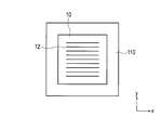
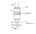
- FIG. 1 is a perspective view showing the configuration of the substrate internal processing apparatus 100.
- the substrate internal processing apparatus 100 includes a stage 110, a stage support unit 120 that supports the stage 110 so as to be movable in the XY directions, and a substrate fixture 130 that is disposed on the stage 110 and fixes the substrate 10. ing.
- the substrate internal processing apparatus 100 includes a laser light source 150 and a laser condensing unit 160, and the laser condensing unit 160 condenses the laser light 190 emitted from the laser light source 150 and irradiates the substrate 10. To do.
- the laser condensing unit 160 includes an objective lens 170 and a plano-convex lens 180.
- FIG. 2 is a top view showing the substrate 10 placed on the stage 110.
- FIG. 3 is a cross-sectional view showing the substrate 10 placed on the stage 110.
- the substrate 10 is held by the substrate fixture 130 on the stage 110.
- the substrate fixture 130 fixes the substrate 10 by a fixing table 125 provided thereon.
- a normal adhesive layer, mechanical chuck, electrostatic chuck or the like can be applied to the fixed table 125.
- the condensing point P of the laser beam 190 focused and irradiated on the substrate 10 forms a locus 12 having a predetermined shape in a region at a predetermined depth from the surface inside the substrate 10, thereby being horizontal to the surface.
- a two-dimensional internal reforming layer 14 can be formed in the direction.
- FIG. 4 is a cross-sectional view for explaining the formation of the light condensing point P and the internal modified layer 14 on the substrate 10, and FIG. 5 is a top view thereof.
- the laser light 190 penetrating into the substrate 10 is irradiated toward the substrate 10 through the laser condensing unit 160, and the thickness direction (optical axis) is applied to a predetermined position inside the substrate 10.
- a condensing point P in the direction (t) and the width direction (direction orthogonal to the optical axis) w is formed.
- the substrate 10 In the vicinity of the condensing point P, the substrate 10 is heated by the laser beam, and after the irradiation is completed, the substrate 10 is cooled by heat conduction and heat radiation.
- the substrate 10 is a single crystal, or a crystalline substrate such as polycrystalline silicon, silicon carbide, or sapphire with sufficiently large crystal grains, the energy and time supplied by the laser beam can be selected appropriately.
- the crystallinity of the substrate 10 in the vicinity of the light spot P can be changed and polycrystallized.
- the condensing point P depends on the repetition frequency and the moving speed of the laser light 190.
- the internal modified layer 14 spreading in a planar shape is formed in parallel with the surface 101 of the substrate 10.
- the substrate 10 is divided into the substrate front surface side 10a and the back surface side 10b through the internal modified layer 14, and the internal modified layer 14 itself is finally removed for the production of the divided substrate. Since it becomes a loss, the thickness t is preferably small. Further, in order to efficiently form the internal modified layer 14 on the substrate 10, it is preferable that the width w of the condensing point P is large.
- the laser condensing unit 160 is configured such that the laser light 190 emitted from the laser condensing unit 160 is axially symmetric with respect to its optical axis, and at the condensing point 190 of the laser light 190 inside the substrate 10,
- the condensing point P2 where the light rays of the component 190b on the outer peripheral side of the laser light 190 intersect is located closer to the laser condensing unit 160 than the condensing point P1 where the light rays of the component on the inner peripheral side 190a of the laser light 190 intersect. It is configured.
- the condensing point P2 of the component 190b on the outer peripheral side of the laser light 190 is more than the condensing point P1 on the inner peripheral side 190a of the laser light 190.
- the objective lens 170 and the plano-convex lens 180 are located at a shallow position from the surface of the substrate 10.
- the laser condensing unit 160 used for forming the condensing point P set in this way inside the substrate 10 having a large refractive index has a condensing point shape adjusting means.
- the laser condensing unit 160 includes an objective lens 170 and a plano-convex lens 180 as a condensing point shape adjusting unit.
- the distance between the surface 101 of the substrate 10 and the internal modified layer 14 is set to the distance L1 between the objective lens 170 and the substrate surface by using the laser condensing unit 160 including the objective lens 170 and the plano-convex lens 180 as a focusing point shape adjusting unit. Can be adjusted mainly. Further, by increasing the distance L2 between the plano-convex lens 180 and the surface 101 of the substrate 10, the position of the condensing point P2 is moved further toward the surface 101 of the substrate 10 with respect to the condensing point P1. Can be made.
- This state can be regarded as a state in which the aberration generated in the laser beam 190 by the substrate 10 is excessively corrected, which can be said to be a “out-of-focus” state in which the focus is excessively corrected.
- the internal modified layer 14 formed at a predetermined depth of the substrate 10 can reduce the thickness t and increase the processing width w per pulse for unknown reasons. become.
- the internal reforming layer 14 is subjected to heating and cooling processes by condensing and irradiating the laser beam 190, so that the substrate 10 is polycrystallized when the substrate 10 is single crystal silicon.
- FIG. 6 is a diagram illustrating the first embodiment.
- the laser condensing unit 160 is represented by a plano-convex lens 180 and the optical axis A is described in the horizontal direction, but the laser beam is collected by the entire laser condensing unit 160 including the plano-convex lens 180. It is what is said.
- the present invention will be described by taking a laser beam 190 incident on a laser condensing unit 160 having condensing point shape adjusting means placed in the atmosphere as an example.
- the laser light 190 is 190-1 to 190-4 in order from the optical axis A.
- the laser condensing unit 160 include an objective lens having a correction ring corresponding to the refractive index of the substrate 10.
- the laser light 190 incident on the laser condensing unit 160 in the atmosphere is collected by the laser condensing unit 160 and is condensed inside the substrate 10 through the surface 101 of the substrate 10 that is also placed in the atmosphere.
- the light rays 190-1 to 190-4 are refracted on the surface 101 of the substrate 10 at different angles by the influence of the refractive index of the substrate 10, respectively, travel inside the substrate 10, and intersect the optical axis A.
- the light at the outermost periphery of the beam (the light beam incident on the condensing unit 160 at a position farthest from the optical axis A) 190-4 is light at a position shallower from the surface 101 of the substrate 10 than the light beam 190-3 at the inner periphery.
- the refraction of the substrate 10 is such that 190-3 crosses the optical axis A closer to the surface 101 than 190-2, and 190-2 crosses the optical axis A closer to the surface 101 than 190-1. Design with the rate in mind.
- the laser condensing unit 160 is set so that the laser light 190 is condensed at a position close to the laser condensing unit 160 as it moves from the inner peripheral side to the outer peripheral side.
- Such a setting can be achieved in the objective lens with a correction ring by setting the thickness of the correction ring larger than the depth of the internal processing region 14 formed at the position of the condensing point P.
- the position of the laser condensing unit 160 with respect to the substrate 10 can be moved by the condensing adjustment unit.
- the condensing adjustment unit adjusts the condensing position, condensing shape, and the like of the laser light 190 on the substrate 10 by adjusting the distance between the laser condensing unit 160 and the substrate 10. Adjustment means are included. Such a condensing adjustment part can be easily realized by using a conventional technique.
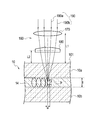
- FIG. 7 is a diagram for explaining a second embodiment of laser beam irradiation on a substrate.
- the laser beam 190 focused by the laser focusing unit 160 is adjusted by the focusing adjustment unit so that the surface of the substrate 10 is focused.
- the position of the laser condensing unit 190 with respect to the substrate 10 is initially set.
- the distance between the laser condensing unit 190 and the surface of the substrate 10 is shortened by a predetermined value from the initial state in which the laser light 190 is focused on the surface of the substrate 10 in the second embodiment by a condensing adjusting unit (not shown).
- a desired condensing point can be formed inside the substrate 10 as in the first embodiment.
- Such an initial setting can be performed not only on the front surface of the substrate 10 but also on the back surface of the substrate 10.
- FIG. 8 is a reference diagram for explaining the aberration in the substrate. This reference diagram shows aberrations that occur when the laser condensing unit 160 is not provided for comparison with the first embodiment. For example, the case where only a normal objective lens is installed corresponds.
- the laser beam 190 is focused on the surface of the substrate 10 as a focal point. From this state, the substrate 10 is moved in the incident direction along the optical axis A so that the laser beam 190 is condensed in the substrate 10. In this case, as shown in FIG. 8B, the light (outer peripheral component) away from the optical axis A is located deeper from the surface of the substrate 10 than the optical axis A (inner peripheral component). To collect light.
- This state is different from the first embodiment in which the outer peripheral component away from the optical axis A is condensed at a position shallower than the inner peripheral component close to the optical axis A.
- the depth of the condensing point on the substrate 10 has an inverse relationship.
- the first embodiment in which the component on the outer peripheral side condenses at a position shallower than the component on the inner peripheral side can be realized only by providing the laser condensing unit 160.
- FIG. 9 is a diagram showing a third embodiment of laser beam irradiation on the substrate.
- adjustment is performed by a condensing point adjusting unit (not shown) so that the distance between the laser condensing unit 160 and the surface of the substrate 10 is shortened, and the laser light is close to the back surface 101b of the substrate 10 in the substrate 10. This is adjusted so that 190 condensing points are formed. Due to this condensing point, the internal modified layer 14 is formed near the back surface 101b of the substrate 10 in parallel with the surface of the substrate 10.
- FIG. 10 is a diagram showing a fourth embodiment of laser beam irradiation on the substrate.
- the laser condensing unit 160 and the surface of the substrate 10 are formed by a condensing adjusting means (not shown). Adjustment is made so that the distance of 101 a is increased, and a condensing point of the laser light 190 is formed in the substrate 10 near the surface 101 a of the substrate 10. Due to this condensing point, the second internal modified layer 14 b is formed near the surface 101 a of the substrate 10 in parallel with the surface 101 a of the substrate 10.
- the internal modified layer 14 is not limited to two layers as in the fourth embodiment, and may be a plurality of layers of two or more layers.
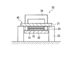
- FIG. 11 is a front view showing the cleaving device.
- the substrate 10 on which the internal modified layer 14 is formed according to the third or fourth embodiment is cleaved in the internal modified layer 14 using this cleaving apparatus.
- the structure body 40 in which the first and second metal plates 20, 21 are bonded to both surfaces of the substrate 10 with an adhesive is placed on the gantry 52.
- the adhesive may be any adhesive that is stronger than the cohesive strength of the polycrystalline grains forming the region near the inner modified layer 14 of the substrate 10.
- an anaerobic acrylic type resin that cures using metal ions as a reaction initiator.
- An adhesive 25 composed of a liquid monomer component can be used.
- the structure 40 may be fixed to the gantry 52 using a through hole provided in the second metal plate 21. In this state, a downward pressing force is applied to the first metal plate 20 by the cleaving jig 54. As a result, the substrate 10 receives a reverse force in both directions of the upper surface and the lower surface bonded to the first and second metal plates 20, 21, and when the force exceeds a predetermined threshold, the substrate 10 is divided, The structure 40 is separated into two upper and lower parts.
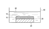
- FIG. 12 is a diagram illustrating a method for peeling the substrate 10 from the metal plate 20 in water.
- the substrate 10 bonded to the metal plates 20 and 21 with the adhesive 25 is immersed in hot water of 80 to 100 ° C. stored in the water tank 60. After a predetermined time has elapsed, the adhesive 25 reacts with water in a predetermined manner, and the adhesive force is lost from the adhesive 25. Therefore, by peeling the adhesive 25 from the substrate 10 in water, the substrate 10 is removed from the metal plates 20, 21. Can be separated.
- the final divided substrate can be obtained by drying the substrate 10 from which the adhesive 25 has been peeled.
- FIG. 13 is a diagram illustrating a specific example of the laser condensing unit.
- the laser condensing unit 160 is realized by a combination of an objective lens 170 having a high NA and a long working distance, and a plano-convex lens 180 provided on the surface side of the substrate 10, for example.
- condensing adjusting means (not shown) adjusts the shape of the condensing point by the distance between the plano-convex lens 80 and the surface of the substrate 10, and the distance between the objective lens 170 and the surface of the substrate 10. It can comprise so that the position of a condensing point may be adjusted.
- FIG. 14 is a diagram showing another specific example of the laser condensing unit.
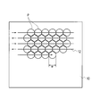
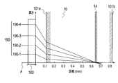
- the correction ring is set to 0.6 mm when the internal processing layer 14 is provided at a position of 300 ⁇ m from the surface of the crystal 10. It can be set so that the light incident on the outer peripheral portion of the condensing unit 160 is condensed on the laser condensing 160 side from the light incident on the inner peripheral portion.
- the internal modified layer 14 when the internal modified layer 14 is formed on the surface side of the substrate 10, it is necessary to increase the distance between the laser focusing means 160 and the surface of the substrate 10.
- beam diameter adjusting means such as an iris diaphragm and a beam expander is provided on the incident side of the laser condensing unit 160, and the outer peripheral component of the laser beam 190 is reduced. The amount of light may be reduced.
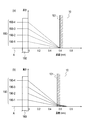
- irradiation examples 1 to 6 performed under various conditions will be described as examples.
- a laser light source 150 of the substrate internal processing apparatus 100 was used with a wavelength of 1064 nm, a repetition frequency of 200 kHz, an output of 1.6 W, and a pulse width of 10 nm.
- the objective lens 200 was moved 0.06 mm toward the surface of the substrate 10 based on this position.
- the setting of the correction ring 210 is set to 0.0 mm and 0.3 mm
- the stage 110 is moved at a speed of 200 mm / s in the x direction, and further 10 ⁇ m is sent in the y direction, so that the objective lens 200 is repeated 10 times.
- the laser beam 190 was radiated from the substrate 10 toward the substrate 10 at intervals of 10 ⁇ m in 10 straight lines.
- the substrate 10 was cleaved at right angles to the linear irradiation direction, and the cross section was observed. As a result, as shown in FIG. 15, substantially the same processing traces having a processing region length of 70 ⁇ m at a depth of 0.3 mm from the mirror-side surface of the substrate 10 were confirmed. Note that the left and right machining marks in the drawing correspond to the case where the correction ring 210 is set to 0.0 mm and 0.3 mm, respectively. This processing trace corresponds to the periodic structure described above.
- the substrate 10 obtained by cutting out a 10 mm ⁇ 10 mm region from this sample was fixed and cured between two metal plates (SUS304, thickness 10 mm) that were filed using an adhesive (SOLARLOC HIK-700M20 manufactured by Denki Kagaku Kogyo).
- SOLARLOC HIK-700M20 manufactured by Denki Kagaku Kogyo
- the substrate 10 was peeled off at the inner processing region 14, and two substrates 10 having a thickness of 10 ⁇ m ⁇ 10 mm and a thickness of 300 ⁇ m and 400 ⁇ m were obtained. .
- the silicon single crystal substrate is exemplified.
- the present invention can be similarly applied to, for example, silicon carbide (SiC).
- the thinly cut substrate can be applied to a solar cell as long as it is a Si substrate. If it is a sapphire substrate, etc., it can be applied to light emitting diodes, laser diodes, etc. If it is SiC, it can be applied to SiC power devices, etc., and it is widely used in the fields of transparent electronics, lighting, hybrid / electric vehicles, etc. Applicable in the field.
Landscapes
- Optics & Photonics (AREA)
- Engineering & Computer Science (AREA)
- Physics & Mathematics (AREA)
- Mechanical Engineering (AREA)
- Plasma & Fusion (AREA)
- Chemical & Material Sciences (AREA)
- Organic Chemistry (AREA)
- Crystallography & Structural Chemistry (AREA)
- Materials Engineering (AREA)
- Metallurgy (AREA)
- Oil, Petroleum & Natural Gas (AREA)
- General Chemical & Material Sciences (AREA)
- Chemical Kinetics & Catalysis (AREA)
- Laser Beam Processing (AREA)
- Processing Of Stones Or Stones Resemblance Materials (AREA)
- Mechanical Treatment Of Semiconductor (AREA)
Applications Claiming Priority (2)
| Application Number | Priority Date | Filing Date | Title |
|---|---|---|---|
| JP2012023333A JP5995045B2 (ja) | 2012-02-06 | 2012-02-06 | 基板加工方法及び基板加工装置 |
| JP2012-023333 | 2012-02-06 |
Publications (1)
| Publication Number | Publication Date |
|---|---|
| WO2013118645A1 true WO2013118645A1 (ja) | 2013-08-15 |
Family
ID=48947409
Family Applications (1)
| Application Number | Title | Priority Date | Filing Date |
|---|---|---|---|
| PCT/JP2013/052322 Ceased WO2013118645A1 (ja) | 2012-02-06 | 2013-02-01 | 基板加工方法及び基板加工装置 |
Country Status (2)
| Country | Link |
|---|---|
| JP (1) | JP5995045B2 (enExample) |
| WO (1) | WO2013118645A1 (enExample) |
Families Citing this family (8)
| Publication number | Priority date | Publication date | Assignee | Title |
|---|---|---|---|---|
| JP2015123466A (ja) * | 2013-12-26 | 2015-07-06 | 信越ポリマー株式会社 | 基板加工装置及び基板加工方法 |
| JP2015123465A (ja) * | 2013-12-26 | 2015-07-06 | 信越ポリマー株式会社 | 基板加工装置及び基板加工方法 |
| DE102015000449A1 (de) | 2015-01-15 | 2016-07-21 | Siltectra Gmbh | Festkörperteilung mittels Stoffumwandlung |
| JP6381110B2 (ja) * | 2014-04-16 | 2018-08-29 | 信越ポリマー株式会社 | 基板加工方法及び基板 |
| EP3399542B1 (de) | 2014-11-27 | 2023-04-12 | Siltectra GmbH | Festkörperteilung mittels stoffumwandlung |
| US10930560B2 (en) | 2014-11-27 | 2021-02-23 | Siltectra Gmbh | Laser-based separation method |
| JP7017728B2 (ja) * | 2017-06-29 | 2022-02-09 | 国立大学法人埼玉大学 | 結晶基板および結晶基板加工方法 |
| JP2020141009A (ja) * | 2019-02-27 | 2020-09-03 | パナソニックIpマネジメント株式会社 | 基板材料およびレーザ加工方法 |
Citations (4)
| Publication number | Priority date | Publication date | Assignee | Title |
|---|---|---|---|---|
| JP2008078236A (ja) * | 2006-09-19 | 2008-04-03 | Hamamatsu Photonics Kk | レーザ加工方法 |
| JP2009200383A (ja) * | 2008-02-25 | 2009-09-03 | Seiko Epson Corp | 基板分割方法、及び表示装置の製造方法 |
| JP2011155070A (ja) * | 2010-01-26 | 2011-08-11 | Saitama Univ | 基板加工方法 |
| JP2012016722A (ja) * | 2010-07-08 | 2012-01-26 | Disco Corp | レーザー加工装置およびレーザー加工方法 |
-
2012
- 2012-02-06 JP JP2012023333A patent/JP5995045B2/ja active Active
-
2013
- 2013-02-01 WO PCT/JP2013/052322 patent/WO2013118645A1/ja not_active Ceased
Patent Citations (4)
| Publication number | Priority date | Publication date | Assignee | Title |
|---|---|---|---|---|
| JP2008078236A (ja) * | 2006-09-19 | 2008-04-03 | Hamamatsu Photonics Kk | レーザ加工方法 |
| JP2009200383A (ja) * | 2008-02-25 | 2009-09-03 | Seiko Epson Corp | 基板分割方法、及び表示装置の製造方法 |
| JP2011155070A (ja) * | 2010-01-26 | 2011-08-11 | Saitama Univ | 基板加工方法 |
| JP2012016722A (ja) * | 2010-07-08 | 2012-01-26 | Disco Corp | レーザー加工装置およびレーザー加工方法 |
Also Published As
| Publication number | Publication date |
|---|---|
| JP5995045B2 (ja) | 2016-09-21 |
| JP2013161976A (ja) | 2013-08-19 |
Similar Documents
| Publication | Publication Date | Title |
|---|---|---|
| JP6044919B2 (ja) | 基板加工方法 | |
| JP5995045B2 (ja) | 基板加工方法及び基板加工装置 | |
| JP6004338B2 (ja) | 単結晶基板製造方法および内部改質層形成単結晶部材 | |
| JP5875121B2 (ja) | 単結晶基板の製造方法および内部改質層形成単結晶部材の製造方法 | |
| JP5875122B2 (ja) | 単結晶基板製造方法および内部改質層形成単結晶部材 | |
| CN103962728B (zh) | 激光加工方法 | |
| TWI687560B (zh) | 晶圓的生成方法 | |
| JP2015123466A (ja) | 基板加工装置及び基板加工方法 | |
| TW201709306A (zh) | 晶圓的生成方法 | |
| JP6004339B2 (ja) | 内部応力層形成単結晶部材および単結晶基板製造方法 | |
| TW201705258A (zh) | 晶圓的生成方法 | |
| WO2007004607A1 (ja) | 加工対象物切断方法 | |
| JP6202696B2 (ja) | 単結晶基板製造方法 | |
| WO2013115352A1 (ja) | 単結晶基板の製造方法、単結晶基板、および、内部改質層形成単結晶部材の製造方法 | |
| CN115770964B (zh) | 一种激光加工脆性材料多焦点裂片装置及其方法 | |
| JP2015123465A (ja) | 基板加工装置及び基板加工方法 | |
| JP2014019120A (ja) | 内部加工層形成単結晶部材の製造方法 | |
| TWI687559B (zh) | 基板製造方法 | |
| JP6202695B2 (ja) | 単結晶基板製造方法 | |
| JP6008565B2 (ja) | 光デバイスウエーハの加工方法 | |
| JP6202694B2 (ja) | 基板加工方法及び基板加工装置 | |
| JP6265522B2 (ja) | 表面3次元構造部材の製造方法 | |
| JP2017070961A (ja) | 基板加工方法及び剥離基板製造方法 | |
| JP2016111146A (ja) | ウエーハの生成方法 | |
| JP2020074468A (ja) | 基板加工方法 |
Legal Events
| Date | Code | Title | Description |
|---|---|---|---|
| 121 | Ep: the epo has been informed by wipo that ep was designated in this application |
Ref document number: 13746404 Country of ref document: EP Kind code of ref document: A1 |
|
| NENP | Non-entry into the national phase |
Ref country code: DE |
|
| 122 | Ep: pct application non-entry in european phase |
Ref document number: 13746404 Country of ref document: EP Kind code of ref document: A1 |