WO2013118645A1 - 基板加工方法及び基板加工装置 - Google Patents
基板加工方法及び基板加工装置 Download PDFInfo
- Publication number
- WO2013118645A1 WO2013118645A1 PCT/JP2013/052322 JP2013052322W WO2013118645A1 WO 2013118645 A1 WO2013118645 A1 WO 2013118645A1 JP 2013052322 W JP2013052322 W JP 2013052322W WO 2013118645 A1 WO2013118645 A1 WO 2013118645A1
- Authority
- WO
- WIPO (PCT)
- Prior art keywords
- substrate
- laser
- condensing
- laser light
- substrate processing
- Prior art date
Links
Images


Classifications
-
- B—PERFORMING OPERATIONS; TRANSPORTING
- B28—WORKING CEMENT, CLAY, OR STONE
- B28D—WORKING STONE OR STONE-LIKE MATERIALS
- B28D5/00—Fine working of gems, jewels, crystals, e.g. of semiconductor material; apparatus or devices therefor
-
- B—PERFORMING OPERATIONS; TRANSPORTING
- B23—MACHINE TOOLS; METAL-WORKING NOT OTHERWISE PROVIDED FOR
- B23K—SOLDERING OR UNSOLDERING; WELDING; CLADDING OR PLATING BY SOLDERING OR WELDING; CUTTING BY APPLYING HEAT LOCALLY, e.g. FLAME CUTTING; WORKING BY LASER BEAM
- B23K26/00—Working by laser beam, e.g. welding, cutting or boring
- B23K26/0006—Working by laser beam, e.g. welding, cutting or boring taking account of the properties of the material involved
-
- B—PERFORMING OPERATIONS; TRANSPORTING
- B23—MACHINE TOOLS; METAL-WORKING NOT OTHERWISE PROVIDED FOR
- B23K—SOLDERING OR UNSOLDERING; WELDING; CLADDING OR PLATING BY SOLDERING OR WELDING; CUTTING BY APPLYING HEAT LOCALLY, e.g. FLAME CUTTING; WORKING BY LASER BEAM
- B23K26/00—Working by laser beam, e.g. welding, cutting or boring
- B23K26/02—Positioning or observing the workpiece, e.g. with respect to the point of impact; Aligning, aiming or focusing the laser beam
- B23K26/04—Automatically aligning, aiming or focusing the laser beam, e.g. using the back-scattered light
- B23K26/046—Automatically focusing the laser beam
-
- B—PERFORMING OPERATIONS; TRANSPORTING
- B23—MACHINE TOOLS; METAL-WORKING NOT OTHERWISE PROVIDED FOR
- B23K—SOLDERING OR UNSOLDERING; WELDING; CLADDING OR PLATING BY SOLDERING OR WELDING; CUTTING BY APPLYING HEAT LOCALLY, e.g. FLAME CUTTING; WORKING BY LASER BEAM
- B23K26/00—Working by laser beam, e.g. welding, cutting or boring
- B23K26/02—Positioning or observing the workpiece, e.g. with respect to the point of impact; Aligning, aiming or focusing the laser beam
- B23K26/06—Shaping the laser beam, e.g. by masks or multi-focusing
- B23K26/062—Shaping the laser beam, e.g. by masks or multi-focusing by direct control of the laser beam
- B23K26/0622—Shaping the laser beam, e.g. by masks or multi-focusing by direct control of the laser beam by shaping pulses
-
- B—PERFORMING OPERATIONS; TRANSPORTING
- B23—MACHINE TOOLS; METAL-WORKING NOT OTHERWISE PROVIDED FOR
- B23K—SOLDERING OR UNSOLDERING; WELDING; CLADDING OR PLATING BY SOLDERING OR WELDING; CUTTING BY APPLYING HEAT LOCALLY, e.g. FLAME CUTTING; WORKING BY LASER BEAM
- B23K26/00—Working by laser beam, e.g. welding, cutting or boring
- B23K26/02—Positioning or observing the workpiece, e.g. with respect to the point of impact; Aligning, aiming or focusing the laser beam
- B23K26/06—Shaping the laser beam, e.g. by masks or multi-focusing
- B23K26/064—Shaping the laser beam, e.g. by masks or multi-focusing by means of optical elements, e.g. lenses, mirrors or prisms
- B23K26/0648—Shaping the laser beam, e.g. by masks or multi-focusing by means of optical elements, e.g. lenses, mirrors or prisms comprising lenses
-
- B—PERFORMING OPERATIONS; TRANSPORTING
- B23—MACHINE TOOLS; METAL-WORKING NOT OTHERWISE PROVIDED FOR
- B23K—SOLDERING OR UNSOLDERING; WELDING; CLADDING OR PLATING BY SOLDERING OR WELDING; CUTTING BY APPLYING HEAT LOCALLY, e.g. FLAME CUTTING; WORKING BY LASER BEAM
- B23K26/00—Working by laser beam, e.g. welding, cutting or boring
- B23K26/08—Devices involving relative movement between laser beam and workpiece
- B23K26/083—Devices involving movement of the workpiece in at least one axial direction
- B23K26/0853—Devices involving movement of the workpiece in at least in two axial directions, e.g. in a plane
-
- B—PERFORMING OPERATIONS; TRANSPORTING
- B23—MACHINE TOOLS; METAL-WORKING NOT OTHERWISE PROVIDED FOR
- B23K—SOLDERING OR UNSOLDERING; WELDING; CLADDING OR PLATING BY SOLDERING OR WELDING; CUTTING BY APPLYING HEAT LOCALLY, e.g. FLAME CUTTING; WORKING BY LASER BEAM
- B23K26/00—Working by laser beam, e.g. welding, cutting or boring
- B23K26/50—Working by transmitting the laser beam through or within the workpiece
- B23K26/53—Working by transmitting the laser beam through or within the workpiece for modifying or reforming the material inside the workpiece, e.g. for producing break initiation cracks
-
- C—CHEMISTRY; METALLURGY
- C30—CRYSTAL GROWTH
- C30B—SINGLE-CRYSTAL GROWTH; UNIDIRECTIONAL SOLIDIFICATION OF EUTECTIC MATERIAL OR UNIDIRECTIONAL DEMIXING OF EUTECTOID MATERIAL; REFINING BY ZONE-MELTING OF MATERIAL; PRODUCTION OF A HOMOGENEOUS POLYCRYSTALLINE MATERIAL WITH DEFINED STRUCTURE; SINGLE CRYSTALS OR HOMOGENEOUS POLYCRYSTALLINE MATERIAL WITH DEFINED STRUCTURE; AFTER-TREATMENT OF SINGLE CRYSTALS OR A HOMOGENEOUS POLYCRYSTALLINE MATERIAL WITH DEFINED STRUCTURE; APPARATUS THEREFOR
- C30B29/00—Single crystals or homogeneous polycrystalline material with defined structure characterised by the material or by their shape
- C30B29/02—Elements
- C30B29/06—Silicon
-
- C—CHEMISTRY; METALLURGY
- C30—CRYSTAL GROWTH
- C30B—SINGLE-CRYSTAL GROWTH; UNIDIRECTIONAL SOLIDIFICATION OF EUTECTIC MATERIAL OR UNIDIRECTIONAL DEMIXING OF EUTECTOID MATERIAL; REFINING BY ZONE-MELTING OF MATERIAL; PRODUCTION OF A HOMOGENEOUS POLYCRYSTALLINE MATERIAL WITH DEFINED STRUCTURE; SINGLE CRYSTALS OR HOMOGENEOUS POLYCRYSTALLINE MATERIAL WITH DEFINED STRUCTURE; AFTER-TREATMENT OF SINGLE CRYSTALS OR A HOMOGENEOUS POLYCRYSTALLINE MATERIAL WITH DEFINED STRUCTURE; APPARATUS THEREFOR
- C30B33/00—After-treatment of single crystals or homogeneous polycrystalline material with defined structure
- C30B33/04—After-treatment of single crystals or homogeneous polycrystalline material with defined structure using electric or magnetic fields or particle radiation
-
- B—PERFORMING OPERATIONS; TRANSPORTING
- B23—MACHINE TOOLS; METAL-WORKING NOT OTHERWISE PROVIDED FOR
- B23K—SOLDERING OR UNSOLDERING; WELDING; CLADDING OR PLATING BY SOLDERING OR WELDING; CUTTING BY APPLYING HEAT LOCALLY, e.g. FLAME CUTTING; WORKING BY LASER BEAM
- B23K2101/00—Articles made by soldering, welding or cutting
- B23K2101/36—Electric or electronic devices
- B23K2101/40—Semiconductor devices
-
- B—PERFORMING OPERATIONS; TRANSPORTING
- B23—MACHINE TOOLS; METAL-WORKING NOT OTHERWISE PROVIDED FOR
- B23K—SOLDERING OR UNSOLDERING; WELDING; CLADDING OR PLATING BY SOLDERING OR WELDING; CUTTING BY APPLYING HEAT LOCALLY, e.g. FLAME CUTTING; WORKING BY LASER BEAM
- B23K2103/00—Materials to be soldered, welded or cut
- B23K2103/50—Inorganic material, e.g. metals, not provided for in B23K2103/02 – B23K2103/26
- B23K2103/52—Ceramics
Definitions
- the present invention relates to a substrate processing method and a substrate processing apparatus for processing a silicon single crystal substrate.
- the semiconductor wafer manufactured in this way is subjected to various processes such as circuit pattern formation in the previous process in order and used in the subsequent process.
- the back surface is back-grinded and thinned. Accordingly, the thickness is adjusted to about 750 ⁇ m to 100 ⁇ m or less, for example, about 75 ⁇ m or 50 ⁇ m.
- a conventional semiconductor wafer is manufactured as described above, and an ingot is cut with a wire saw, and a cutting allowance larger than the thickness of the wire saw is required for cutting, so a thin semiconductor wafer with a thickness of 0.1 mm or less It was very difficult to manufacture and the product rate was not improved.
- a processed layer having a thickness of about 100 ⁇ m was formed inside the silicon substrate. For this reason, when a large number of thin substrates having a thickness of about 0.1 mm are sliced from the crystalline substrate, there is a limit to the material yield. For example, even if the infrared observation aberration enhancing material for silicon is removed, the thickness of the processed layer cannot be reduced greatly.
- a wafer is referred to as a substrate unless otherwise specified.
- the present invention has been made to solve the above problems, and is a substrate processing apparatus and method for forming an internal processing layer by laser light irradiation inside a crystalline substrate and peeling the internal processing layer as a boundary, It is an object of the present invention to provide a substrate processing apparatus and a substrate processing method for efficiently forming an internal processing layer with a wide selection of laser light sources, a thin internal processing layer, and irradiation with a small number of laser pulses.
- a substrate processing apparatus is a substrate processing apparatus for processing a crystal substrate, and irradiates a laser light source and laser light from the laser light source toward the surface of the substrate.
- the modified layer is formed inside the substrate by moving the laser condensing unit, and the laser condensing unit condenses the laser beam in an axial symmetry with respect to an optical axis, and the laser condensing unit is disposed inside the substrate.
- the light incident on the outer peripheral part of the laser is condensed on the laser condensing means side from the light incident on the inner peripheral part of the laser condensing means.
- the laser condensing means preferably has condensing adjusting means for adjusting condensing of the laser light.
- the condensing adjusting means can adjust the condensing position to a depth from the front surface to the back surface of the substrate.
- the irradiated laser beam is preferably pulsed.
- the modified layer is preferably formed in parallel with the surface of the substrate.
- the surface of the substrate is preferably a mirror surface.
- the substrate is preferably a silicon single crystal substrate or a silicon carbide single crystal substrate.
- the apparatus further includes substrate holding means for holding the substrate, and the laser holding means and the substrate held by the substrate holding means are relatively moved.
- a substrate processing method is a substrate processing method for processing a crystal substrate, wherein the laser light source irradiates a laser beam from the laser light source toward the surface of the substrate and focuses the laser beam inside the substrate.
- the light means condenses the laser light axially symmetrically with respect to the optical axis, and light incident on the outer peripheral portion of the laser condensing means is incident on the inner peripheral portion of the laser condensing means inside the substrate.
- the laser is condensed on the laser condensing means side.
- the method further has a condensing adjustment step of adjusting the condensing of the laser light in the laser condensing means.
- the condensing position is preferably adjusted to a depth from the front surface to the back surface of the substrate.
- the laser light is preferably condensed on the surface of the substrate.
- the condensing adjustment step is adjusted so that the laser beam is condensed on the back surface of the substrate.
- the modified layer is preferably formed in parallel with the surface of the substrate.
- the condensing point is moved to the laser condensing unit side by the condensing adjusting unit to form a second modified layer.
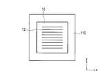
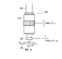
- FIG. 1 is a perspective view showing the configuration of the substrate internal processing apparatus 100.
- the substrate internal processing apparatus 100 includes a stage 110, a stage support unit 120 that supports the stage 110 so as to be movable in the XY directions, and a substrate fixture 130 that is disposed on the stage 110 and fixes the substrate 10. ing.
- the substrate internal processing apparatus 100 includes a laser light source 150 and a laser condensing unit 160, and the laser condensing unit 160 condenses the laser light 190 emitted from the laser light source 150 and irradiates the substrate 10. To do.
- the laser condensing unit 160 includes an objective lens 170 and a plano-convex lens 180.
- FIG. 2 is a top view showing the substrate 10 placed on the stage 110.
- FIG. 3 is a cross-sectional view showing the substrate 10 placed on the stage 110.
- the substrate 10 is held by the substrate fixture 130 on the stage 110.
- the substrate fixture 130 fixes the substrate 10 by a fixing table 125 provided thereon.
- a normal adhesive layer, mechanical chuck, electrostatic chuck or the like can be applied to the fixed table 125.
- the condensing point P of the laser beam 190 focused and irradiated on the substrate 10 forms a locus 12 having a predetermined shape in a region at a predetermined depth from the surface inside the substrate 10, thereby being horizontal to the surface.
- a two-dimensional internal reforming layer 14 can be formed in the direction.
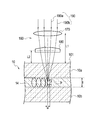
- FIG. 4 is a cross-sectional view for explaining the formation of the light condensing point P and the internal modified layer 14 on the substrate 10, and FIG. 5 is a top view thereof.
- the laser light 190 penetrating into the substrate 10 is irradiated toward the substrate 10 through the laser condensing unit 160, and the thickness direction (optical axis) is applied to a predetermined position inside the substrate 10.
- a condensing point P in the direction (t) and the width direction (direction orthogonal to the optical axis) w is formed.
- the substrate 10 In the vicinity of the condensing point P, the substrate 10 is heated by the laser beam, and after the irradiation is completed, the substrate 10 is cooled by heat conduction and heat radiation.
- the substrate 10 is a single crystal, or a crystalline substrate such as polycrystalline silicon, silicon carbide, or sapphire with sufficiently large crystal grains, the energy and time supplied by the laser beam can be selected appropriately.
- the crystallinity of the substrate 10 in the vicinity of the light spot P can be changed and polycrystallized.
- the condensing point P depends on the repetition frequency and the moving speed of the laser light 190.
- the internal modified layer 14 spreading in a planar shape is formed in parallel with the surface 101 of the substrate 10.
- the substrate 10 is divided into the substrate front surface side 10a and the back surface side 10b through the internal modified layer 14, and the internal modified layer 14 itself is finally removed for the production of the divided substrate. Since it becomes a loss, the thickness t is preferably small. Further, in order to efficiently form the internal modified layer 14 on the substrate 10, it is preferable that the width w of the condensing point P is large.
- the laser condensing unit 160 is configured such that the laser light 190 emitted from the laser condensing unit 160 is axially symmetric with respect to its optical axis, and at the condensing point 190 of the laser light 190 inside the substrate 10,
- the condensing point P2 where the light rays of the component 190b on the outer peripheral side of the laser light 190 intersect is located closer to the laser condensing unit 160 than the condensing point P1 where the light rays of the component on the inner peripheral side 190a of the laser light 190 intersect. It is configured.
- the condensing point P2 of the component 190b on the outer peripheral side of the laser light 190 is more than the condensing point P1 on the inner peripheral side 190a of the laser light 190.
- the objective lens 170 and the plano-convex lens 180 are located at a shallow position from the surface of the substrate 10.
- the laser condensing unit 160 used for forming the condensing point P set in this way inside the substrate 10 having a large refractive index has a condensing point shape adjusting means.
- the laser condensing unit 160 includes an objective lens 170 and a plano-convex lens 180 as a condensing point shape adjusting unit.
- the distance between the surface 101 of the substrate 10 and the internal modified layer 14 is set to the distance L1 between the objective lens 170 and the substrate surface by using the laser condensing unit 160 including the objective lens 170 and the plano-convex lens 180 as a focusing point shape adjusting unit. Can be adjusted mainly. Further, by increasing the distance L2 between the plano-convex lens 180 and the surface 101 of the substrate 10, the position of the condensing point P2 is moved further toward the surface 101 of the substrate 10 with respect to the condensing point P1. Can be made.
- This state can be regarded as a state in which the aberration generated in the laser beam 190 by the substrate 10 is excessively corrected, which can be said to be a “out-of-focus” state in which the focus is excessively corrected.
- the internal modified layer 14 formed at a predetermined depth of the substrate 10 can reduce the thickness t and increase the processing width w per pulse for unknown reasons. become.
- the internal reforming layer 14 is subjected to heating and cooling processes by condensing and irradiating the laser beam 190, so that the substrate 10 is polycrystallized when the substrate 10 is single crystal silicon.
- FIG. 6 is a diagram illustrating the first embodiment.
- the laser condensing unit 160 is represented by a plano-convex lens 180 and the optical axis A is described in the horizontal direction, but the laser beam is collected by the entire laser condensing unit 160 including the plano-convex lens 180. It is what is said.
- the present invention will be described by taking a laser beam 190 incident on a laser condensing unit 160 having condensing point shape adjusting means placed in the atmosphere as an example.
- the laser light 190 is 190-1 to 190-4 in order from the optical axis A.
- the laser condensing unit 160 include an objective lens having a correction ring corresponding to the refractive index of the substrate 10.
- the laser light 190 incident on the laser condensing unit 160 in the atmosphere is collected by the laser condensing unit 160 and is condensed inside the substrate 10 through the surface 101 of the substrate 10 that is also placed in the atmosphere.
- the light rays 190-1 to 190-4 are refracted on the surface 101 of the substrate 10 at different angles by the influence of the refractive index of the substrate 10, respectively, travel inside the substrate 10, and intersect the optical axis A.
- the light at the outermost periphery of the beam (the light beam incident on the condensing unit 160 at a position farthest from the optical axis A) 190-4 is light at a position shallower from the surface 101 of the substrate 10 than the light beam 190-3 at the inner periphery.
- the refraction of the substrate 10 is such that 190-3 crosses the optical axis A closer to the surface 101 than 190-2, and 190-2 crosses the optical axis A closer to the surface 101 than 190-1. Design with the rate in mind.
- the laser condensing unit 160 is set so that the laser light 190 is condensed at a position close to the laser condensing unit 160 as it moves from the inner peripheral side to the outer peripheral side.
- Such a setting can be achieved in the objective lens with a correction ring by setting the thickness of the correction ring larger than the depth of the internal processing region 14 formed at the position of the condensing point P.
- the position of the laser condensing unit 160 with respect to the substrate 10 can be moved by the condensing adjustment unit.
- the condensing adjustment unit adjusts the condensing position, condensing shape, and the like of the laser light 190 on the substrate 10 by adjusting the distance between the laser condensing unit 160 and the substrate 10. Adjustment means are included. Such a condensing adjustment part can be easily realized by using a conventional technique.
- FIG. 7 is a diagram for explaining a second embodiment of laser beam irradiation on a substrate.
- the laser beam 190 focused by the laser focusing unit 160 is adjusted by the focusing adjustment unit so that the surface of the substrate 10 is focused.
- the position of the laser condensing unit 190 with respect to the substrate 10 is initially set.
- the distance between the laser condensing unit 190 and the surface of the substrate 10 is shortened by a predetermined value from the initial state in which the laser light 190 is focused on the surface of the substrate 10 in the second embodiment by a condensing adjusting unit (not shown).
- a desired condensing point can be formed inside the substrate 10 as in the first embodiment.
- Such an initial setting can be performed not only on the front surface of the substrate 10 but also on the back surface of the substrate 10.
- FIG. 8 is a reference diagram for explaining the aberration in the substrate. This reference diagram shows aberrations that occur when the laser condensing unit 160 is not provided for comparison with the first embodiment. For example, the case where only a normal objective lens is installed corresponds.
- the laser beam 190 is focused on the surface of the substrate 10 as a focal point. From this state, the substrate 10 is moved in the incident direction along the optical axis A so that the laser beam 190 is condensed in the substrate 10. In this case, as shown in FIG. 8B, the light (outer peripheral component) away from the optical axis A is located deeper from the surface of the substrate 10 than the optical axis A (inner peripheral component). To collect light.
- This state is different from the first embodiment in which the outer peripheral component away from the optical axis A is condensed at a position shallower than the inner peripheral component close to the optical axis A.
- the depth of the condensing point on the substrate 10 has an inverse relationship.
- the first embodiment in which the component on the outer peripheral side condenses at a position shallower than the component on the inner peripheral side can be realized only by providing the laser condensing unit 160.
- FIG. 9 is a diagram showing a third embodiment of laser beam irradiation on the substrate.
- adjustment is performed by a condensing point adjusting unit (not shown) so that the distance between the laser condensing unit 160 and the surface of the substrate 10 is shortened, and the laser light is close to the back surface 101b of the substrate 10 in the substrate 10. This is adjusted so that 190 condensing points are formed. Due to this condensing point, the internal modified layer 14 is formed near the back surface 101b of the substrate 10 in parallel with the surface of the substrate 10.
- FIG. 10 is a diagram showing a fourth embodiment of laser beam irradiation on the substrate.
- the laser condensing unit 160 and the surface of the substrate 10 are formed by a condensing adjusting means (not shown). Adjustment is made so that the distance of 101 a is increased, and a condensing point of the laser light 190 is formed in the substrate 10 near the surface 101 a of the substrate 10. Due to this condensing point, the second internal modified layer 14 b is formed near the surface 101 a of the substrate 10 in parallel with the surface 101 a of the substrate 10.
- the internal modified layer 14 is not limited to two layers as in the fourth embodiment, and may be a plurality of layers of two or more layers.
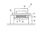
- FIG. 11 is a front view showing the cleaving device.
- the substrate 10 on which the internal modified layer 14 is formed according to the third or fourth embodiment is cleaved in the internal modified layer 14 using this cleaving apparatus.
- the structure body 40 in which the first and second metal plates 20, 21 are bonded to both surfaces of the substrate 10 with an adhesive is placed on the gantry 52.
- the adhesive may be any adhesive that is stronger than the cohesive strength of the polycrystalline grains forming the region near the inner modified layer 14 of the substrate 10.
- an anaerobic acrylic type resin that cures using metal ions as a reaction initiator.
- An adhesive 25 composed of a liquid monomer component can be used.
- the structure 40 may be fixed to the gantry 52 using a through hole provided in the second metal plate 21. In this state, a downward pressing force is applied to the first metal plate 20 by the cleaving jig 54. As a result, the substrate 10 receives a reverse force in both directions of the upper surface and the lower surface bonded to the first and second metal plates 20, 21, and when the force exceeds a predetermined threshold, the substrate 10 is divided, The structure 40 is separated into two upper and lower parts.
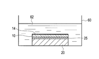
- FIG. 12 is a diagram illustrating a method for peeling the substrate 10 from the metal plate 20 in water.
- the substrate 10 bonded to the metal plates 20 and 21 with the adhesive 25 is immersed in hot water of 80 to 100 ° C. stored in the water tank 60. After a predetermined time has elapsed, the adhesive 25 reacts with water in a predetermined manner, and the adhesive force is lost from the adhesive 25. Therefore, by peeling the adhesive 25 from the substrate 10 in water, the substrate 10 is removed from the metal plates 20, 21. Can be separated.
- the final divided substrate can be obtained by drying the substrate 10 from which the adhesive 25 has been peeled.
- FIG. 13 is a diagram illustrating a specific example of the laser condensing unit.
- the laser condensing unit 160 is realized by a combination of an objective lens 170 having a high NA and a long working distance, and a plano-convex lens 180 provided on the surface side of the substrate 10, for example.
- condensing adjusting means (not shown) adjusts the shape of the condensing point by the distance between the plano-convex lens 80 and the surface of the substrate 10, and the distance between the objective lens 170 and the surface of the substrate 10. It can comprise so that the position of a condensing point may be adjusted.
- FIG. 14 is a diagram showing another specific example of the laser condensing unit.
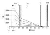
- the correction ring is set to 0.6 mm when the internal processing layer 14 is provided at a position of 300 ⁇ m from the surface of the crystal 10. It can be set so that the light incident on the outer peripheral portion of the condensing unit 160 is condensed on the laser condensing 160 side from the light incident on the inner peripheral portion.
- the internal modified layer 14 when the internal modified layer 14 is formed on the surface side of the substrate 10, it is necessary to increase the distance between the laser focusing means 160 and the surface of the substrate 10.
- beam diameter adjusting means such as an iris diaphragm and a beam expander is provided on the incident side of the laser condensing unit 160, and the outer peripheral component of the laser beam 190 is reduced. The amount of light may be reduced.
- irradiation examples 1 to 6 performed under various conditions will be described as examples.
- a laser light source 150 of the substrate internal processing apparatus 100 was used with a wavelength of 1064 nm, a repetition frequency of 200 kHz, an output of 1.6 W, and a pulse width of 10 nm.
- the objective lens 200 was moved 0.06 mm toward the surface of the substrate 10 based on this position.
- the setting of the correction ring 210 is set to 0.0 mm and 0.3 mm
- the stage 110 is moved at a speed of 200 mm / s in the x direction, and further 10 ⁇ m is sent in the y direction, so that the objective lens 200 is repeated 10 times.
- the laser beam 190 was radiated from the substrate 10 toward the substrate 10 at intervals of 10 ⁇ m in 10 straight lines.
- the substrate 10 was cleaved at right angles to the linear irradiation direction, and the cross section was observed. As a result, as shown in FIG. 15, substantially the same processing traces having a processing region length of 70 ⁇ m at a depth of 0.3 mm from the mirror-side surface of the substrate 10 were confirmed. Note that the left and right machining marks in the drawing correspond to the case where the correction ring 210 is set to 0.0 mm and 0.3 mm, respectively. This processing trace corresponds to the periodic structure described above.
- the substrate 10 obtained by cutting out a 10 mm ⁇ 10 mm region from this sample was fixed and cured between two metal plates (SUS304, thickness 10 mm) that were filed using an adhesive (SOLARLOC HIK-700M20 manufactured by Denki Kagaku Kogyo).
- SOLARLOC HIK-700M20 manufactured by Denki Kagaku Kogyo
- the substrate 10 was peeled off at the inner processing region 14, and two substrates 10 having a thickness of 10 ⁇ m ⁇ 10 mm and a thickness of 300 ⁇ m and 400 ⁇ m were obtained. .
- the silicon single crystal substrate is exemplified.
- the present invention can be similarly applied to, for example, silicon carbide (SiC).
- the thinly cut substrate can be applied to a solar cell as long as it is a Si substrate. If it is a sapphire substrate, etc., it can be applied to light emitting diodes, laser diodes, etc. If it is SiC, it can be applied to SiC power devices, etc., and it is widely used in the fields of transparent electronics, lighting, hybrid / electric vehicles, etc. Applicable in the field.
Landscapes
- Optics & Photonics (AREA)
- Engineering & Computer Science (AREA)
- Physics & Mathematics (AREA)
- Mechanical Engineering (AREA)
- Plasma & Fusion (AREA)
- Chemical & Material Sciences (AREA)
- Organic Chemistry (AREA)
- Crystallography & Structural Chemistry (AREA)
- Materials Engineering (AREA)
- Metallurgy (AREA)
- Oil, Petroleum & Natural Gas (AREA)
- General Chemical & Material Sciences (AREA)
- Chemical Kinetics & Catalysis (AREA)
- Laser Beam Processing (AREA)
- Processing Of Stones Or Stones Resemblance Materials (AREA)
- Mechanical Treatment Of Semiconductor (AREA)
Abstract
薄いシリコン基板を製品率を確保して提供する。レーザ光源150と、レーザ光源150からのレーザ光190を基板10の表面101に向けて照射し、基板10内部にレーザ光を集光するレーザ集光部160と、レーザ集光部160を基板10上に非接触に配置する位置決め手段とを有し、レーザ集光部160と基板10を相対的に移動させて、基板10内部に改質層14を形成するものであって、レーザ集光部160は、レーザ光190を光軸に軸対称に集光するとともに、基板10内部において、レーザ集光部160の外周部に入射した光が、レーザ集光部160の内周部に入射した光より、レーザ集光部160で集光するように構成されている。
Description
本発明は、シリコン単結晶基板を加工する基板加工方法及び基板加工装置に関する。
従来、シリコン(Si)ウェハに代表される半導体ウェハを製造する場合には、石英るつぼ内に溶融されたシリコン融液から凝固した円柱形のインゴットを適切な長さのブロックに切断して、その周縁部を目標の直径になるよう研削し、その後、ブロック化されたインゴットをワイヤソーによりウェハ形にスライスして半導体ウェハを製造するようにしている(例えば、特許文献1および2参照。)。
このようにして製造された半導体ウェハは、前工程で回路パターンの形成等、各種の処理が順次施されて後工程に供され、この後工程で裏面がバックグラインド処理されて薄片化が図られることにより、厚さが約750μmから100μm以下、例えば75μmや50μm程度に調整される。
従来における半導体ウェハは、以上のように製造され、インゴットがワイヤソーにより切断され、しかも、切断の際にワイヤソーの太さ以上の切り代が必要となるので、厚さ0.1mm以下の薄い半導体ウェハを製造することが非常に困難であり、製品率も向上しないという問題があった。
一方、高開口数の集光レンズにガラス板からなる収差増強材を組み合わせ、波長1064nmのパルス状レーザによりシリコンウエハの内部に加工を施した後、これを剛性基板に貼りあわせ、剥離することで薄い単結晶シリコン基板を得る技術が開示されている(特許文献3参照。)。
この技術によると、シリコン基板内部に厚み100μm程度の加工層が形成されていた。このため、結晶性基板から厚さ0.1mm程度の薄い基板を多数スライスする場合、材料歩留まりに限界があった。また、例えば、シリコン用の赤外線観察用収差増強材を外しても、加工層の厚みは大きく減少させることができなかった。
さらに、NAが0.5程度の対物レンズを使用した場合、加工層の厚みは減少するが、光量が減少して加工層の処理が十分に施されず、実際の剥離は困難であった。これに対して、照射回数を増やして加工層の処理を十分に施そうとすると、2次元の加工領域を1μmピッチの照射で埋め尽くす必要があるため、膨大な回数の照射パルスが必用になり、実用化には照射時間の問題が存在していた。
なお、この明細書中においては、別記する場合を除いてウェハのことを基板と称することにする。
本発明は、上記課題に対してなされたもので、結晶性基板の内部にレーザ光照射による内部加工層を形成し、内部加工層を境に剥離するための基板加工装置及び方法であって、レーザ光源の選択肢が広く、内部加工層の厚みが薄く、かつ、少ない数のレーザパルス照射で、内部加工層を効率的に形成する基板加工装置および基板加工方法を提供することを目的とする。
上述の課題を解決するために、本発明に係る基板加工装置は、結晶基板を加工する基板加工装置であって、レーザ光源と、前記レーザ光源からのレーザ光を基板の表面に向けて照射し、基板内部にレーザ光を集光するレーザ集光手段と、前記レーザ集光手段を前記基板上に非接触に配置する位置決め手段とを有し、前記レーザ集光手段と前記基板を相対的に移動させて、前記基板内部に改質層を形成するものであって、前記レーザ集光手段は、レーザ光を光軸に軸対称に集光するとともに、前記基板内部において、前記レーザ集光手段の外周部に入射した光が、前記レーザ集光手段の内周部に入射した光より、前記レーザ集光手段側で集光するように構成されているものである。
前記レーザ集光手段は、レーザ光の集光を調整する集光調整手段を有することが好ましい。
前記集光調整手段は、前記基板における表面から裏面に至るまでの深さに集光位置を調整することができることが好ましい。
前記照射されるレーザ光は、パルス状であることが好ましい。
前記改質層は、前記基板の表面と平行に形成されることが好ましい。
前記基板の表面は、鏡面であることが好ましい。
前記基板は、シリコン単結晶基板又はシリコンカーバイド単結晶基板であることが好ましい。
前記基板を保持する基板保持手段をさらに有し、前記レーザ集光手段と前記基板保持手段に保持された前記基板を相対的に移動させることが好ましい。
本発明に係る基板加工方法は、結晶基板を加工する基板加工方法であって、前記レーザ光源からのレーザ光を基板の表面に向けて照射し、前記基板内部にレーザ光を集光するレーザ集光手段を基板上に非接触に配置する位置決め工程と、前記レーザ集光手段と前記基板を相対的に移動させて、前記基板内部に改質層を形成する工程とを有し、前記レーザ集光手段は、レーザ光を光軸に軸対称に集光するとともに、前記基板内部において、前記レーザ集光手段の外周部に入射した光が、前記レーザ集光手段の内周部に入射した光より、前記レーザ集光手段側で集光するように構成されているものである。
前記レーザ集光手段におけるレーザ光の集光を調整する集光調整工程をさらに有することが好ましい。
前記集光調整工程は、前記基板における表面から裏面に至るまでの深さに集光位置を調整することが好ましい。
前記集光調整工程は、前記レーザ光が前記基板の表面に集光することが好ましい。
前記集光調整工程は、前記レーザ光が前記基板の裏面に集光するように調整することが好ましい。
前記改質層は、前記基板の表面と平行に形成されることが好ましい。
前記改質層を形成した後、前記集光調整手段により集光点を前記レーザ集光手段側に移動し、第2の改質層を形成することが好ましい。
前記基板を保持する工程をさらに有することが好ましい。
次に、図面を参照して、本発明の実施の形態を説明する。以下の図面の記載において、同一又は類似の部分には同一又は類似の符号を付している。ただし、図面は模式的なものであり、厚みと平面寸法との関係、各層の厚みの比率等は現実のものとは異なることに留意すべきである。したがって、具体的な厚みや寸法は以下の説明を参酌して判断すべきものである。又、図面相互間においても互いの寸法の関係や比率が異なる部分が含まれていることはもちろんである。
又、以下に示す実施の形態は、この発明の技術的思想を具体化するための装置や方法を例示するものであって、この発明の実施の形態は、構成部品の材質、形状、構造、配置等を下記のものに特定するものでない。この発明の実施の形態は、特許請求の範囲において、種々の変更を加えることができる。
(基板内部加工装置の構成)
図1は、基板内部加工装置100の構成を示す斜視図である。基板内部加工装置100は、ステージ110と、ステージ110がXY方向に移動可能なように支持するステージ支持部120と、ステージ110上に配置され、基板10を固定する基板固定具130とを有している。
図1は、基板内部加工装置100の構成を示す斜視図である。基板内部加工装置100は、ステージ110と、ステージ110がXY方向に移動可能なように支持するステージ支持部120と、ステージ110上に配置され、基板10を固定する基板固定具130とを有している。
また、基板内部加工装置100は、レーザ光源150と、レーザ集光部160を有し、レーザ集光部160は、レーザ光源150から発したレーザ光190を集光して基板10に向けて照射する。レーザ集光部160は、対物レンズ170及び平凸レンズ180を有している。
図2は、ステージ110上に置いた基板10を示す上面図である。図3は、ステージ110上に置いた基板10を示す断面図である。
基板10は、ステージ110上において基板固定具130によって保持されている。基板固定具130は、その上に設けられた固定テーブル125によって基板10を固定している。固定テーブル125には、通常の粘着層、機械的なチャック、静電チャックなどが適用可能である。
基板10に集光して照射されるレーザ光190の集光点Pは、基板10の内部において、表面から所定の深さの領域に所定の形状の軌跡12を形成することで、表面に水平方向に2次元状の内部改質層14を形成することができる。
図4は、基板10における集光点Pと内部改質層14の形成を説明する断面図、図5は、その上面図である。基板内部加工装置100においては、基板10の内部に浸透するレーザ光190は、レーザ集光部160を介して基板10に向けて照射され、基板10内部の所定位置に、厚さ方向(光軸方向)t、幅方向(光軸と直交方向)wの集光点Pを形成する。
集光点Pの近傍では、基板10はレーザ光により加熱され、照射終了後は基板10の熱伝導および熱輻射により冷却される。基板10が単結晶、若しくは十分に結晶粒の大きな多結晶のシリコンや炭化ケイ素、あるいはサファイアのような結晶性基板の場合、レーザ光で供給されるエネルギーと時間を適切に選択することで、集光点P近傍の基板10の結晶性を変化させ、多結晶化させることができる。
また、レーザ光190としてパルス状のレーザを使用し、基板10をレーザ集光部160に対して相対的に移動させると、集光点Pは、レーザ光190の繰返し周波数と、移動速度に応じ、基板10の表面101と並行に並ぶ列を形成し、さらにこの列を複数、配列することで、基板10の表面101と平行に、面状に広がった内部改質層14が形成される。
レーザ光190に適切なパルス状レーザを採用し、適切な条件で基板10と集光手段160を相対的に移動させることで、基板10の表面101にダメージを与えることなく、他の領域と結晶状態の変化させた表面101に平行な2次元状の内部改質層14は、単結晶状態の他の領域と物性が異なるため、比較的小さな力でこの領域を境に、基板10を分割することができる。
内部改質層14を介して基板10を基板表面側10aと裏面側10bに分割し、利用することを考えるとき、内部改質層14自体は分割基板の作成のために最終的に除去されて損失となるため、その厚さtは小さいことが好ましい。また、基板10に内部改質層14を効率よく形成するためには集光点Pの幅wは大きいことが好ましい。
本実施の形態においては、レーザ集光部160は、レーザ集光部160の出射するレーザ光190がその光軸について軸対称であり、基板10の内部のレーザ光190の集光点190において、レーザ光190の外周側の成分190bの光線が交差する集光点P2が、レーザ光190の内周側190aの成分の光線が交差する集光点P1よりもレーザ集光部160側にあるように構成されている。
換言すると、基板10の表面はレーザ集光部160に対向しているので、レーザ光190の外周側の成分190bの集光点P2は、レーザ光190の内周側190aの集光点P1よりも、対物レンズ170及び平凸レンズ180側、すなわち基板10の表面から浅い位置にある。
このような、屈折率の大きな基板10内部にこのように設定される集光点Pを形成するために使用されるレーザ集光部160は、集光点形状調整手段を有する。図4では、レーザ集光部160は、対物レンズ170及び集光点形状調整手段として平凸レンズ180で構成される。
大気中で、収差なく集光する対物レンズ170で集光されるレーザ光190で、外周部の光ほど平凸レンズ180で大きく曲げることで、シリコンのような屈折率の大きな素材で形成された基板10の内部に集光することが可能になる。
この対物レンズ170及び集光点形状調整手段としての平凸レンズ180からなるレーザ集光部160を用いて、基板10の表面101と内部改質層14の距離を対物レンズ170と基板表面の距離L1で主に調整することができる。また、平凸レンズ180と基板10の表面101の距離L2を大きくすることで、集光点Pにおいて、集光点P1を基準に、集光点P2の位置をより基板10の表面101側に移動させることができる。
この状態は、基板10によりレーザ光190に生じた収差が過剰に補正された状態であると見なすことができ、いわばピントを過剰に補正した「ピンボケ」状態であるということができる。このような状態で、基板10の所定の深さに形成される内部改質層14は厚さtを小さくし、かつ、理由は不明であるがパルスあたりの加工幅wを大きくすることが可能になる。
内部改質層14は、レーザ光190を集光して照射することによって、加熱と冷却のプロセスを経るため、基板10が、単結晶シリコンの場合、多結晶化する。
このようなレーザ集光部160を用い、基板10に対してレーザ光190を照射する実施の形態について説明する。図6は、第1の実施の形態を示す図である。図6においては、便宜上、レーザ集光部160を平凸レンズ180により代表し、光軸Aを横方向に記載するが、レーザ光の集光は平凸レンズ180を含むレーザ集光部160全体によって行われるものである。
この第1の実施の形態では、大気中に置かれた集光点形状調整手段を有するレーザ集光部160に入射するレーザ光190を例に本発明を説明する。レーザ光190は便宜上、光軸Aに近い順に190-1~190-4とする。レーザ集光部160としては、例えば基板10の屈折率に対応した補正環を有する対物レンズが例示される。
大気中で、レーザ集光部160に入射したレーザ光190は、レーザ集光部160によって集光され、同じく大気中に置かれた基板10の表面101を介して基板10の内部に集光される。光線190-1~4は、それぞれ基板10の屈折率の影響で、異なる角度で基板10の表面101で屈折し基板10の内部を進んで、光軸Aと交差する。
ビーム最外周の光(光軸Aから最も遠い位置で、集光部160に入射する光線)190-4は、その内周にある光線190-3よりも基板10の表面101から浅い位置で光軸Aと交差するし、さらに、190-3は190-2よりも表面101側で、さらに190-2は190-1よりも表面101側で光軸Aと交差するように、基板10の屈折率を考慮して設計する。
換言すると、レーザ光190は内周側から外周側に移るに従い、レーザ集光部160に近い位置で集光するように、レーザ集光部160を設定する。このような設定は、補正環付き対物レンズでは、補正環の厚さ設定を、集光点Pの位置に形成される内部加工領域14の深さより大きく設定することで達成することができる。
なお、レーザ集光部160の基板10に対する位置は、集光調整部によって移動することができる。この集光調整部は、レーザ集光部160と基板10の距離等を調整することにより基板10におけるレーザ光190の集光位置、集光形状等を調整するものであり、前述の集光形状調整手段を含むものである。このような集光調整部は従来技術を用いて容易に実現することができる。
図7は、基板に対するレーザ光の照射の第2の実施の形態を説明する図である。第2の実施の形態では、レーザ集光部160によって集光されたレーザ光190が基板10の表面を焦点とするように集光調整部によって調整されている。
この第2の実施の形態は、例えば、第1の実施の形態で示したように基板10内部に集光点を設定する前に、レーザ集光部190の基板10に対する位置を初期設定するときに使用することができる。すなわち、図示しない集光調整部によって、第2の実施の形態においてレーザ光190が基板10の表面を焦点とする初期状態からレーザ集光部190と基板10の表面の距離を所定値にわたって短縮することにより、第1の実施の形態のように基板10内部に所望の集光点を形成することができる。なお、このような初期設定は、基板10の表面に限らず、基板10の裏面に焦点を合わせて行うこともできる。
図8は、基板における収差を説明する参考図である。この参考図は、第1の実施の形態と対比するために、レーザ集光部160を設けない場合に生じる収差を示すものである。例えば、通常の対物レンズのみを設置した場合が相当する。
図8(a)においては、第2の実施の形態と同様に、基板の10の表面を焦点としてレーザ光190が集光されている。この状態から基板10を光軸Aに沿って入射方向に移動してレーザ光190が基板10内で集光するようにする。この場合、図8(b)に示すように、光軸Aから離れた光(外周側の成分)のが、光軸Aに近い(内周側の成分)よりも基板10の表面から深い位置で集光するようになる。
この状態は、光軸Aから離れた外周側の成分が光軸Aに近い内周側の成分より浅い位置に集光する第1の実施の形態とは、光線の光軸Aからの距離と基板10における集光点の深さが逆の関係となっている。換言すると、外周側の成分が内周側の成分より浅い位置に集光する第1の実施の形態は、レーザ集光部160を設けることによって初めて実現が可能となるものである。
図9は、基板に対するレーザ光の照射の第3の実施の形態を示す図である。第3の実施の形態においては、図示しない集光点調整部によってレーザ集光部160と基板10の表面の距離を短縮するように調整し、基板10内において基板10の裏面101b近くにレーザ光190の集光点が形成されるように調整したものである。この集光点によって、基板の10の裏面101b近くに基板10の表面に平行に内部改質層14が形成される。
図10は、基板に対するレーザ光の照射の第4の実施の形態を示す図である。第4の実施の形態においては、第3の実施の形態により基板10の裏面101b近くに内部改質層14aを形成した後、図示しない集光調整手段によってレーザ集光部160と基板10の表面101aの距離が拡大するように調整し、基板10内において基板10の表面101a近くにレーザ光190の集光点が形成されるようにしたものである。この集光点によって、基板10の表面101a近くに基板10の表面101aに平行に第2の内部改質層14bが形成される。なお、内部改質層14は、この第4の実施例のように2層に限らず、2層以上の複数層であってもよい。
(基板の割断)
図11は、割断装置を示す正面図である。第3又は第4の実施の形態によって内部改質層14が形成された基板10は、この割断装置を用いて内部改質層14において割断される。
図11は、割断装置を示す正面図である。第3又は第4の実施の形態によって内部改質層14が形成された基板10は、この割断装置を用いて内部改質層14において割断される。
この割断装置50において、架台52上に、基板10の両面に第1及び第2の金属板20、21が接着剤にて接着されてなる構造体40が載置される。この接着剤としては、基板10の内部改質層14近傍領域を形成する多結晶粒の凝集力よりも強い接着剤であればよく、例えば金属イオンを反応開始剤として硬化する嫌気性アクリル系二液モノマー成分からなる接着剤25を使用することができる。
構造体40は、第2の金属板21に設けられた貫孔を利用して架台52に固定してよい。この状態において、第1の金属板20に割断冶具54によって下向きの押圧力を印加する。これによって、基板10は第1及び第2の金属板20、21に接着した上面及び下面の両面の方向に逆向きの力を受け、力が所定の閾値を越えると、基板10は分割され、構造体40は上下2つに分離される。
(基板の剥離)
図12は、水中で金属板20から基板10を剥離する方法を説明する図である。水槽60に蓄えた80~100℃の温水に、金属板20、21に接着剤25で接着された基板10を浸す。所定時間経過すると接着剤25が水と所定の反応を生じ、接着剤25から接着力が失われるので、水中で基板10から接着剤25を剥離することにより、金属板20、21から基板10を分離することができる。
図12は、水中で金属板20から基板10を剥離する方法を説明する図である。水槽60に蓄えた80~100℃の温水に、金属板20、21に接着剤25で接着された基板10を浸す。所定時間経過すると接着剤25が水と所定の反応を生じ、接着剤25から接着力が失われるので、水中で基板10から接着剤25を剥離することにより、金属板20、21から基板10を分離することができる。
このように接着剤25が剥離された基板10を乾燥することによって、最終的な分割した基板を得ることができる。なお、第4の実施の形態のように内部改質層14a、14bが複数存在する場合には、基板10の割断の工程を複数回繰り返すことにより複数の内部改質層ごとに分割することができる。
(レーザ集光部の具体例)
図13は、レーザ集光部の具体例を示す図である。この具体例において、レーザ集光部160は、例えば高NAで作動距離の長い対物レンズ170と基板10の表面側に設けた平凸レンズ180との組み合わせによって実現している。
図13は、レーザ集光部の具体例を示す図である。この具体例において、レーザ集光部160は、例えば高NAで作動距離の長い対物レンズ170と基板10の表面側に設けた平凸レンズ180との組み合わせによって実現している。
具体的には、厚み1mmの単結晶シリコンからなる基板10の内部加工については、基板10の表面側より、0.14mmの位置に焦点距離15mmのガラス製の平凸レンズ180(シグマ光機:SLB-10-15P)を置き、NA=0.3の対物レンズ170(シグマ光機:EPL-10)に組み合わせることができる。
このようなレーザ集光部160においては、図示しない集光調整手段は、平凸レンズ80と基板10の表面の距離で集光点の形状を調整し、対物レンズ170と基板10の表面の距離で集光点の位置を調整するように構成することができる。
図14は、レーザ集光部の他の具体例を示す図である。他の具体例では、NA=0.5~0.9の補正環を有するシリコン用の赤外線対物レンズにより実現している。具体的には、例えばオリンパス製レンズLCPLN100XIRを使用する場合、内部加工層14を結晶10の表面から300μmの位置に設けるときに補正環を0.6mmに設定することで、基板10内において、レーザ集光部160の外周部に入射した光が、内周部に入射した光より、レーザ集光160側で集光するように設定することができる。
この他の実施例によると、前述の実施例のように対物レンズ170及び平凸レンズ180という複数の構成部材を必要とすることなく、単一の補正環付き対物レンズにより構成できるので、装置の構成が簡単になり、操作が容易になる。
なお、この他の具体例においては、基板10のより表面側に内部改質層14を形成する場合、レーザ集光手段160と基板10の表面との距離を大きくする必要がある。この場合、レーザ光190が基板10の表面に及ぼす影響を抑制するため、虹彩絞りやビームエクスパンダなどのビーム径調整手段をレーザ集光部160の入射側に設けレーザ光190の外周側成分の光量を低減することがある。
以下、実施例として各種条件について実施した照射例1~6について説明する。これらの照射例1~6においては、基板内部加工装置100のレーザ光源150としては、波長1064nm、繰り返し周波数200kHz、出力1.6W、パルス幅10nmのものを使用した。
〔照射例1〕
基板内部加工装置100において、x軸、y軸方向にそれぞれ最大速度200mm/sで移動可能なxyステージ110上に、大きさ50×50mm、厚み0.7mm、表面が鏡面加工された単結晶シリコンからなる基板10を載置固定した。
基板内部加工装置100において、x軸、y軸方向にそれぞれ最大速度200mm/sで移動可能なxyステージ110上に、大きさ50×50mm、厚み0.7mm、表面が鏡面加工された単結晶シリコンからなる基板10を載置固定した。
レーザ集光部160は、NA=0.85のシリコン用補正環210付の顕微鏡用赤外対物レンズ200(オリンパス製LCPLN100XIR)を用いた。そして、補正環210を0mmに設定した上、参照光により観察し、対物レンズ200から照射される光が基板10の表面上に焦点を形成するように、対物レンズ200を基板10の表面に対して位置決めをした。
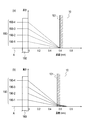
ついで、この位置を基準に対物レンズ200を基板10の表面に向けて0.06mm移動させた。この状態で補正環210の設定を0.0mm、0.3mmとし、ステージ110をx方向に200mm/sの速度で移動させ、さらにy方向に10μm送ることを10回繰り返すことで、対物レンズ200から基板10に向けてレーザ光190を10μm間隔でそれぞれ10本の直線状に照射した。
この基板10を直線状の照射方向に直角に劈開を行い、断面を観察した。この結果、図15に示すように、基板10鏡面側表面から0.3mmの深さにそれぞれ加工領域の長さが70μmのほぼ同じ加工痕を確認した。なお、図中の左側及び右側の加工痕は、それぞれ補正環210を0.0mm及び0.3mmを設定したときに対応している。なお、この加工跡は、前述した周期的構造に相当するものである。
〔照射例2〕
この照射例2においては、対物レンズ200の補正環210を0.6mmに設定した。他の条件は照射例1と同様である。この照射例2では、図16に示すように、基板10における加工痕の長さは30μmに減少し、かつ隣接する加工痕同士が連結する状態が確認できた。
この照射例2においては、対物レンズ200の補正環210を0.6mmに設定した。他の条件は照射例1と同様である。この照射例2では、図16に示すように、基板10における加工痕の長さは30μmに減少し、かつ隣接する加工痕同士が連結する状態が確認できた。
〔照射例3〕
この照射例3においては、照射例2と同様に対物レンズ200補正環210を0.6mmに設定した。そして、基板10を載置したステージ110のy方向送りを1μmピッチで50000回とすることで、基板10の50×50mmの領域を加工したサンプルを作成した。他の条件は照射例1と同様である。
この照射例3においては、照射例2と同様に対物レンズ200補正環210を0.6mmに設定した。そして、基板10を載置したステージ110のy方向送りを1μmピッチで50000回とすることで、基板10の50×50mmの領域を加工したサンプルを作成した。他の条件は照射例1と同様である。
このサンプルから10mm×10mmの領域を切り出した基板10を、接着剤(電気化学工業製 SOLARLOC HIK-700M20)を用いてヤスリかけした2枚の金属板(SUS304、厚み10mm)板の間に固定硬化後、2枚の金属板を剥離したところ、上下面の金属板に内部加工領域を境に剥離した基板10が接着した状態で得られた。
これを100℃の熱水中に4時間放置することで、内部加工領域14を境に基板10が剥離し、10mm×10mmでそれぞれ厚さ300μm、400μm厚の2枚の基板10が得られた。
〔照射例4〕
この照射例4においては、対物レンズ200の補正環210を0.6mmに設定し、ステージ110の7方向への送りを2μmピッチで25000回とした。他の条件は照射例3と同様である。この照射例4においても、内部加工領域14を境に基板10が剥離し、10mm×10mmでそれぞれ厚さ300μm、400μm厚の2枚のシリコン基板が得られた。
この照射例4においては、対物レンズ200の補正環210を0.6mmに設定し、ステージ110の7方向への送りを2μmピッチで25000回とした。他の条件は照射例3と同様である。この照射例4においても、内部加工領域14を境に基板10が剥離し、10mm×10mmでそれぞれ厚さ300μm、400μm厚の2枚のシリコン基板が得られた。
〔照射例5〕
この照射例5においては、対物レンズ200の補正環210を0.3mmに設定した。他の条件は、照射例3と同様である。この照射例5においても、照射例3と同様の処理によって基板10を内部改質層14を境に剥離することを試みた。しかしながら、基板10と接着剤層の界面で剥離が発生し、内部改質層14を境として剥離することはできなかった。
この照射例5においては、対物レンズ200の補正環210を0.3mmに設定した。他の条件は、照射例3と同様である。この照射例5においても、照射例3と同様の処理によって基板10を内部改質層14を境に剥離することを試みた。しかしながら、基板10と接着剤層の界面で剥離が発生し、内部改質層14を境として剥離することはできなかった。
〔照射例6〕
この照射例6においては、対物レンズ200の補正環210を0.0mmにした。他の条件は、照射例5と同様である。この照射例6においても、基板10と接着剤層の界面で剥離が発生し、内部改質層14を境として剥離することはできなかった。
この照射例6においては、対物レンズ200の補正環210を0.0mmにした。他の条件は、照射例5と同様である。この照射例6においても、基板10と接着剤層の界面で剥離が発生し、内部改質層14を境として剥離することはできなかった。
なお、上記の実施の形態においてはシリコン単結晶基板について例示したが、例えばシリコンカーバイド(SiC)等にも同様に適用することができる。
本発明の基板加工装置及び方法により基板を効率良く薄く形成することができることから、薄く切り出された基板は、Si基板であれば、太陽電池に応用可能であり、また、GaN系半導体デバイスなどのサファイア基板などであれば、発光ダイオード、レーザダイオードなどに応用可能であり、SiCなどであれば、SiC系パワーデバイスなどに応用可能であり、透明エレクトロニクス分野、照明分野、ハイブリッド/電気自動車分野など幅広い分野において適用可能である。
10 基板
14 内部改質層
100 基板内部加工装置
110 ステージ
120 ステージ支持部
150 レーザ光源
160 レーザ集光部
170 対物レンズ
180 平凸レンズ
190 レーザ光
14 内部改質層
100 基板内部加工装置
110 ステージ
120 ステージ支持部
150 レーザ光源
160 レーザ集光部
170 対物レンズ
180 平凸レンズ
190 レーザ光
Claims (16)
- 結晶基板を加工する基板加工装置であって、
レーザ光源と、
前記レーザ光源からのレーザ光を基板の表面に向けて照射し、基板内部にレーザ光を集光するレーザ集光手段と、
前記レーザ集光手段を前記基板上に非接触に配置する位置決め手段とを有し、
前記レーザ集光手段と前記基板を相対的に移動させて、前記基板内部に改質層を形成するものであって、
前記レーザ集光手段は、レーザ光を光軸に軸対称に集光するとともに、前記基板内部において、前記レーザ集光手段の外周部に入射した光が、前記レーザ集光手段の内周部に入射した光より、前記レーザ集光手段側で集光するように構成されていることを特徴とする基板加工装置。 - 前記レーザ集光手段は、レーザ光の集光を調整する集光調整手段を有することを特徴とする請求項1記載の基板加工装置。
- 前記集光調整手段は、前記基板における表面から裏面に至るまでの深さに集光位置を調整することができることを特徴とする請求項2記載の基板加工装置。
- 前記照射されるレーザ光は、パルス状であることを特徴とする請求項1記載の基板加工装置。
- 前記改質層は、前記基板の表面と平行に形成されることを特徴とする請求項1記載の基板加工装置。
- 前記基板の表面は、鏡面であることを特徴とする請求項1記載の基板加工装置。
- 前記基板は、シリコン単結晶基板又はシリコンカーバイド単結晶基板である請求項1記載の基板加工装置。
- 前記基板を保持する基板保持手段をさらに有し、前記レーザ集光手段と前記基板保持手段に保持された前記基板を相対的に移動させることを特徴とする請求項1記載の基板加工装置。
- 結晶基板を加工する基板加工方法であって、
レーザ光源からのレーザ光を基板の表面に向けて照射し、前記基板内部にレーザ光を集光するレーザ集光手段を基板上に非接触に配置する位置決め工程と、
前記レーザ集光手段と前記基板を相対的に移動させて、前記基板内部に改質層を形成する工程とを有し、
前記レーザ集光手段は、レーザ光を光軸に軸対称に集光するとともに、前記基板内部において、前記レーザ集光手段の外周部に入射した光が、前記レーザ集光手段の内周部に入射した光より、前記レーザ集光手段側で集光するように構成されていることを特徴とする基板加工方法。 - 前記レーザ集光手段におけるレーザ光の集光を調整する集光調整工程をさらに有することを特徴とする請求項9記載の基板加工方法。
- 前記集光調整工程は、前記基板における表面から裏面に至るまでの深さに集光位置を調整することができることを特徴とする請求項10記載の基板加工方法。
- 前記集光調整工程は、前記レーザ光が前記基板の表面に集光するように調整することを特徴とする請求項11記載の基板加工方法。
- 前記集光調整工程は、前記レーザ光が前記基板の裏面に集光するように調整することを特徴とする請求項11記載の基板加工方法。
- 前記改質層は、前記基板の表面と平行に形成されることを特徴とする請求項10記載の基板加工方法。
- 前記改質層を形成した後、前記集光調整工程により集光点を前記レーザ集光手段側に移動し、第2の改質層を形成することを特徴とする請求項14記載の基板加工方法。
- 前記基板を保持する工程をさらに有することを特徴とする請求項9記載の基板加工方法。
Applications Claiming Priority (2)
| Application Number | Priority Date | Filing Date | Title |
|---|---|---|---|
| JP2012023333A JP5995045B2 (ja) | 2012-02-06 | 2012-02-06 | 基板加工方法及び基板加工装置 |
| JP2012-023333 | 2012-02-06 |
Publications (1)
| Publication Number | Publication Date |
|---|---|
| WO2013118645A1 true WO2013118645A1 (ja) | 2013-08-15 |
Family
ID=48947409
Family Applications (1)
| Application Number | Title | Priority Date | Filing Date |
|---|---|---|---|
| PCT/JP2013/052322 WO2013118645A1 (ja) | 2012-02-06 | 2013-02-01 | 基板加工方法及び基板加工装置 |
Country Status (2)
| Country | Link |
|---|---|
| JP (1) | JP5995045B2 (ja) |
| WO (1) | WO2013118645A1 (ja) |
Families Citing this family (8)
| Publication number | Priority date | Publication date | Assignee | Title |
|---|---|---|---|---|
| JP2015123465A (ja) * | 2013-12-26 | 2015-07-06 | 信越ポリマー株式会社 | 基板加工装置及び基板加工方法 |
| JP2015123466A (ja) * | 2013-12-26 | 2015-07-06 | 信越ポリマー株式会社 | 基板加工装置及び基板加工方法 |
| DE102015000449A1 (de) | 2015-01-15 | 2016-07-21 | Siltectra Gmbh | Festkörperteilung mittels Stoffumwandlung |
| JP6381110B2 (ja) * | 2014-04-16 | 2018-08-29 | 信越ポリマー株式会社 | 基板加工方法及び基板 |
| CN108838562B (zh) * | 2014-11-27 | 2021-08-17 | 西尔特克特拉有限责任公司 | 借助于材料转化的固体分开 |
| CN107000125B (zh) | 2014-11-27 | 2022-08-12 | 西尔特克特拉有限责任公司 | 基于激光器的分离方法 |
| JP7017728B2 (ja) * | 2017-06-29 | 2022-02-09 | 国立大学法人埼玉大学 | 結晶基板および結晶基板加工方法 |
| JP2020141009A (ja) * | 2019-02-27 | 2020-09-03 | パナソニックIpマネジメント株式会社 | 基板材料およびレーザ加工方法 |
Citations (4)
| Publication number | Priority date | Publication date | Assignee | Title |
|---|---|---|---|---|
| JP2008078236A (ja) * | 2006-09-19 | 2008-04-03 | Hamamatsu Photonics Kk | レーザ加工方法 |
| JP2009200383A (ja) * | 2008-02-25 | 2009-09-03 | Seiko Epson Corp | 基板分割方法、及び表示装置の製造方法 |
| JP2011155070A (ja) * | 2010-01-26 | 2011-08-11 | Saitama Univ | 基板加工方法 |
| JP2012016722A (ja) * | 2010-07-08 | 2012-01-26 | Disco Corp | レーザー加工装置およびレーザー加工方法 |
-
2012
- 2012-02-06 JP JP2012023333A patent/JP5995045B2/ja active Active
-
2013
- 2013-02-01 WO PCT/JP2013/052322 patent/WO2013118645A1/ja active Application Filing
Patent Citations (4)
| Publication number | Priority date | Publication date | Assignee | Title |
|---|---|---|---|---|
| JP2008078236A (ja) * | 2006-09-19 | 2008-04-03 | Hamamatsu Photonics Kk | レーザ加工方法 |
| JP2009200383A (ja) * | 2008-02-25 | 2009-09-03 | Seiko Epson Corp | 基板分割方法、及び表示装置の製造方法 |
| JP2011155070A (ja) * | 2010-01-26 | 2011-08-11 | Saitama Univ | 基板加工方法 |
| JP2012016722A (ja) * | 2010-07-08 | 2012-01-26 | Disco Corp | レーザー加工装置およびレーザー加工方法 |
Also Published As
| Publication number | Publication date |
|---|---|
| JP2013161976A (ja) | 2013-08-19 |
| JP5995045B2 (ja) | 2016-09-21 |
Similar Documents
| Publication | Publication Date | Title |
|---|---|---|
| WO2013118645A1 (ja) | 基板加工方法及び基板加工装置 | |
| JP6044919B2 (ja) | 基板加工方法 | |
| JP6004338B2 (ja) | 単結晶基板製造方法および内部改質層形成単結晶部材 | |
| JP5875121B2 (ja) | 単結晶基板の製造方法および内部改質層形成単結晶部材の製造方法 | |
| JP5875122B2 (ja) | 単結晶基板製造方法および内部改質層形成単結晶部材 | |
| JP5843393B2 (ja) | 単結晶基板の製造方法、単結晶基板、および、内部改質層形成単結晶部材の製造方法 | |
| JP6004339B2 (ja) | 内部応力層形成単結晶部材および単結晶基板製造方法 | |
| JP2016197700A (ja) | ウエーハの生成方法 | |
| JP2015123466A (ja) | 基板加工装置及び基板加工方法 | |
| JP6549014B2 (ja) | 光デバイスウエーハの加工方法 | |
| KR20120012451A (ko) | 레이저 가공 방법 | |
| JP2015123465A (ja) | 基板加工装置及び基板加工方法 | |
| JP6818273B2 (ja) | 基板加工方法 | |
| JP2014019120A (ja) | 内部加工層形成単結晶部材の製造方法 | |
| CN107636805B (zh) | 半导体元件的制造方法及制造装置 | |
| JP2017070961A (ja) | 基板加工方法及び剥離基板製造方法 | |
| JP6202694B2 (ja) | 基板加工方法及び基板加工装置 | |
| TWI687559B (zh) | 基板製造方法 | |
| JP6202695B2 (ja) | 単結晶基板製造方法 | |
| JP6202696B2 (ja) | 単結晶基板製造方法 | |
| US10373855B2 (en) | Method for processing a wafer and method for processing a carrier | |
| JP2006024782A (ja) | 基板製造方法、および基板製造装置 | |
| JP6887641B2 (ja) | ガラススライシング方法 | |
| JP2017177214A (ja) | 基板加工方法および基板加工装置 | |
| JP2020074468A (ja) | 基板加工方法 |
Legal Events
| Date | Code | Title | Description |
|---|---|---|---|
| 121 | Ep: the epo has been informed by wipo that ep was designated in this application |
Ref document number: 13746404 Country of ref document: EP Kind code of ref document: A1 |
|
| NENP | Non-entry into the national phase |
Ref country code: DE |
|
| 122 | Ep: pct application non-entry in european phase |
Ref document number: 13746404 Country of ref document: EP Kind code of ref document: A1 |