WO2013111629A1 - 固体撮像素子および駆動方法、並びに電子機器 - Google Patents
固体撮像素子および駆動方法、並びに電子機器 Download PDFInfo
- Publication number
- WO2013111629A1 WO2013111629A1 PCT/JP2013/050407 JP2013050407W WO2013111629A1 WO 2013111629 A1 WO2013111629 A1 WO 2013111629A1 JP 2013050407 W JP2013050407 W JP 2013050407W WO 2013111629 A1 WO2013111629 A1 WO 2013111629A1
- Authority
- WO
- WIPO (PCT)
- Prior art keywords
- signal
- state
- unit
- output
- pixel
- Prior art date
Links
- 238000000034 method Methods 0.000 title claims abstract description 19
- 238000001514 detection method Methods 0.000 claims abstract description 69
- 238000000926 separation method Methods 0.000 claims description 102
- 238000012546 transfer Methods 0.000 claims description 53
- 238000006243 chemical reaction Methods 0.000 claims description 41
- 238000003384 imaging method Methods 0.000 claims description 41
- 230000000875 corresponding effect Effects 0.000 claims description 30
- 239000011159 matrix material Substances 0.000 claims description 14
- 230000001276 controlling effect Effects 0.000 claims description 9
- 230000002596 correlated effect Effects 0.000 claims description 4
- 238000005070 sampling Methods 0.000 claims description 4
- 238000005516 engineering process Methods 0.000 abstract description 27
- 238000005286 illumination Methods 0.000 abstract description 3
- 230000002349 favourable effect Effects 0.000 abstract 1
- 238000012545 processing Methods 0.000 description 42
- 238000009792 diffusion process Methods 0.000 description 31
- 238000000605 extraction Methods 0.000 description 18
- 230000003321 amplification Effects 0.000 description 15
- 238000003199 nucleic acid amplification method Methods 0.000 description 15
- 238000010586 diagram Methods 0.000 description 10
- 239000003990 capacitor Substances 0.000 description 9
- 238000002955 isolation Methods 0.000 description 6
- 238000009825 accumulation Methods 0.000 description 5
- 239000000284 extract Substances 0.000 description 5
- 230000003287 optical effect Effects 0.000 description 4
- 229910021420 polycrystalline silicon Inorganic materials 0.000 description 4
- 229920005591 polysilicon Polymers 0.000 description 4
- 239000000758 substrate Substances 0.000 description 4
- 230000006870 function Effects 0.000 description 3
- 239000010410 layer Substances 0.000 description 3
- 238000010408 sweeping Methods 0.000 description 3
- 238000012937 correction Methods 0.000 description 2
- 230000000694 effects Effects 0.000 description 2
- 238000005401 electroluminescence Methods 0.000 description 2
- 230000003071 parasitic effect Effects 0.000 description 2
- 230000002093 peripheral effect Effects 0.000 description 2
- 239000004065 semiconductor Substances 0.000 description 2
- XUIMIQQOPSSXEZ-UHFFFAOYSA-N Silicon Chemical compound [Si] XUIMIQQOPSSXEZ-UHFFFAOYSA-N 0.000 description 1
- 230000002411 adverse Effects 0.000 description 1
- 230000003139 buffering effect Effects 0.000 description 1
- 238000007796 conventional method Methods 0.000 description 1
- 230000002542 deteriorative effect Effects 0.000 description 1
- 239000011229 interlayer Substances 0.000 description 1
- 239000004973 liquid crystal related substance Substances 0.000 description 1
- 239000000203 mixture Substances 0.000 description 1
- 238000012986 modification Methods 0.000 description 1
- 230000004048 modification Effects 0.000 description 1
- 239000002245 particle Substances 0.000 description 1
- 238000005096 rolling process Methods 0.000 description 1
- 229910052710 silicon Inorganic materials 0.000 description 1
- 239000010703 silicon Substances 0.000 description 1
Images


Classifications
-
- H—ELECTRICITY
- H01—ELECTRIC ELEMENTS
- H01L—SEMICONDUCTOR DEVICES NOT COVERED BY CLASS H10
- H01L27/00—Devices consisting of a plurality of semiconductor or other solid-state components formed in or on a common substrate
- H01L27/14—Devices consisting of a plurality of semiconductor or other solid-state components formed in or on a common substrate including semiconductor components sensitive to infrared radiation, light, electromagnetic radiation of shorter wavelength or corpuscular radiation and specially adapted either for the conversion of the energy of such radiation into electrical energy or for the control of electrical energy by such radiation
- H01L27/144—Devices controlled by radiation
- H01L27/146—Imager structures
- H01L27/14643—Photodiode arrays; MOS imagers
-
- H—ELECTRICITY
- H04—ELECTRIC COMMUNICATION TECHNIQUE
- H04N—PICTORIAL COMMUNICATION, e.g. TELEVISION
- H04N25/00—Circuitry of solid-state image sensors [SSIS]; Control thereof
- H04N25/50—Control of the SSIS exposure
- H04N25/57—Control of the dynamic range
- H04N25/59—Control of the dynamic range by controlling the amount of charge storable in the pixel, e.g. modification of the charge conversion ratio of the floating node capacitance
-
- H—ELECTRICITY
- H04—ELECTRIC COMMUNICATION TECHNIQUE
- H04N—PICTORIAL COMMUNICATION, e.g. TELEVISION
- H04N25/00—Circuitry of solid-state image sensors [SSIS]; Control thereof
- H04N25/60—Noise processing, e.g. detecting, correcting, reducing or removing noise
- H04N25/616—Noise processing, e.g. detecting, correcting, reducing or removing noise involving a correlated sampling function, e.g. correlated double sampling [CDS] or triple sampling
-
- H—ELECTRICITY
- H04—ELECTRIC COMMUNICATION TECHNIQUE
- H04N—PICTORIAL COMMUNICATION, e.g. TELEVISION
- H04N25/00—Circuitry of solid-state image sensors [SSIS]; Control thereof
- H04N25/60—Noise processing, e.g. detecting, correcting, reducing or removing noise
- H04N25/65—Noise processing, e.g. detecting, correcting, reducing or removing noise applied to reset noise, e.g. KTC noise related to CMOS structures by techniques other than CDS
-
- H—ELECTRICITY
- H04—ELECTRIC COMMUNICATION TECHNIQUE
- H04N—PICTORIAL COMMUNICATION, e.g. TELEVISION
- H04N25/00—Circuitry of solid-state image sensors [SSIS]; Control thereof
- H04N25/70—SSIS architectures; Circuits associated therewith
- H04N25/76—Addressed sensors, e.g. MOS or CMOS sensors
- H04N25/77—Pixel circuitry, e.g. memories, A/D converters, pixel amplifiers, shared circuits or shared components
- H04N25/771—Pixel circuitry, e.g. memories, A/D converters, pixel amplifiers, shared circuits or shared components comprising storage means other than floating diffusion
Definitions
- the present technology relates to a solid-state imaging device, a driving method, and an electronic device, and in particular, achieves a good S / N in each of a signal at high illuminance and a signal at low illuminance, and appropriately removes reset noise.
- the present invention relates to a solid-state imaging device, a driving method, and an electronic device.
- CMOS image sensor is known as a solid-state image sensor (image sensor).
- image sensor image sensor
- CMOS image sensors are used in various mobile terminal devices such as digital still cameras, digital video cameras, and camera-equipped mobile phones.
- the FD is composed of two capacitors.
- the signal (S1) sensed by one capacitor is used, and when the charge is large, two capacitors are used. It is proposed to use the signal (S2) sensed in (see, for example, Patent Document 1 to Patent Document 3).
- the first problem is that at least one of S1 and S2 cannot remove reset noise even if a difference is taken
- the second problem is an adverse effect due to the fact that addition is required to obtain a signal at high illumination. That is, if the addition is not performed at the time of low illuminance, the linearity of the signal is deteriorated before and after the start of addition, and if the addition is also performed at the time of low illuminance, noise is increased. In particular, when the signal of S1 exceeds the range in which the linearity of the pixel output can be guaranteed, this problem becomes significant.
- the reset level (N) is obtained by resetting the PD after outputting S1 and S2, as in the so-called three-transistor pixel. Even if the difference from N is taken, reset noise remains in both signals.
- the FD is divided into two.
- the reset noise and the accumulation period are included in S2.
- the FD dark current of the minute is superimposed.
- the signals are output in the order of N1, S1, S2, and N2, the column signal processing circuit needs to be able to cope with whichever reset level or signal level comes first.
- the present technology is disclosed in view of such a situation, and can realize good S / N in each of a signal at high illuminance and a signal at low illuminance, and can appropriately remove reset noise. It is what you want to do.
- a first aspect of the present technology includes a pixel region in which a plurality of pixels are arranged, and the pixel includes a photoelectric conversion unit that performs photoelectric conversion, a transfer unit that transfers charges from the photoelectric conversion unit, and the transfer
- a plurality of detection units for detecting charges transferred by the unit, a reset unit for resetting the plurality of detection units, a connection separation control unit for controlling connection or separation of the plurality of detection units, and a potential of the detection unit
- the output unit outputs a connection state reset level signal and a connection state output signal when the connection separation control unit is connected to the plurality of detection units, and the output unit outputs a connection state reset level signal and a connection state output signal.
- connection separation control unit outputs a separation state reset level signal and a separation state output signal in a state where the plurality of detection units are separated, and a difference between the connection state reset level signal and the connection state output signal Than the first pixel signal is generated, which is a solid-state imaging device in which the second pixel signal is generated by the difference between the separated state the reset level signal and the separated state output signal.
- This pixel signal can be output as a pixel signal related to the pixel.
- the difference between the signals output from the output unit can be calculated by the difference calculation unit in which the pixels are arranged in a two-dimensional matrix and are arranged corresponding to the columns of the pixels.
- CDS Correlated Double Sampling
- the pixels are arranged in a two-dimensional matrix and are arranged corresponding to columns in the pixels, and the connection state reset level signal, the separation state reset level signal, the separation state output signal, and the connection state output signal are respectively
- the difference between the signals output from the output unit can be calculated by a difference calculation unit having a latch circuit to hold.
- the pixels are arranged in a two-dimensional matrix and are arranged corresponding to the columns in the pixels, and count the level of the connection state reset level signal in one direction and count the level of the connection state output signal in the other direction.
- a differential operation unit having a second up / down counter that counts the level of the separation state reset level signal in one direction and counts the level of the separation state output signal in the other direction.
- a first aspect of the present technology includes a pixel region in which a plurality of pixels are arranged, and the pixel includes a photoelectric conversion unit that performs photoelectric conversion, a transfer unit that transfers charges from the photoelectric conversion unit, and the transfer
- a plurality of detection units for detecting charges transferred by the unit, a reset unit for resetting the plurality of detection units, a connection separation control unit for controlling connection or separation of the plurality of detection units, and a potential of the detection unit
- a solid-state imaging device driving method comprising: an output unit that outputs a signal corresponding to the output unit, wherein the output unit has a connection state reset level signal in a state where the connection separation control unit connects the plurality of detection units; A connection state output signal is output, and the connection separation control unit outputs a separation state reset level signal and a separation state output signal in a state where the plurality of detection units are separated, and the connection state reset level signal is output.
- the first pixel signal by the difference between the connected state output signal is generated, it
- the detection unit in the reset signal output operation, in the connection state in which the plurality of detection units are connected, the detection unit is reset, and a connection state reset level signal is output.
- a separated state which is the separated state of the detection unit
- a separated state reset level signal is output.
- a separated state output signal is output in the separated state, and a connected state output signal is output in the connected state. Is output.
- a first pixel signal is generated by calculating a difference between the connection state reset level signal and the connection state output signal, and a difference between the separation state reset level signal and the separation state output signal is calculated. Two pixel signals are generated.
- a second aspect of the present technology includes a pixel region in which a plurality of pixels are arranged, and the pixel includes a photoelectric conversion unit that performs photoelectric conversion, a transfer unit that transfers charges from the photoelectric conversion unit, and the transfer
- a plurality of detection units for detecting charges transferred by the unit, a reset unit for resetting the plurality of detection units, a connection separation control unit for controlling connection or separation of the plurality of detection units, and a potential of the detection unit
- the output unit outputs a connection state reset level signal and a connection state output signal in a state where the connection separation control unit connects the plurality of detection units
- the connection separation control unit outputs a separation state reset level signal and a separation state output signal in a state where the plurality of detection units are separated, and a difference between the connection state reset level signal and the connection state output signal Than the first pixel signal is generated, which is an electronic apparatus including the solid-state imaging device in which the second pixel signal is generated by the difference between the separated state the reset level signal and
- the detection unit in the reset signal output operation, in the connection state in which the plurality of detection units are connected, the detection unit is reset, and a connection state reset level signal is output.
- a separated state which is the separated state of the detection unit
- a separated state reset level signal is output.
- a separated state output signal is output in the separated state, and a connected state output signal is output in the connected state. Is output.
- a first pixel signal is generated by calculating a difference between the connection state reset level signal and the connection state output signal, and a difference between the separation state reset level signal and the separation state output signal is calculated. Two pixel signals are generated.
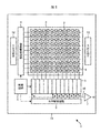
- FIG. 1 is a block diagram illustrating a configuration example of a CMOS image sensor according to an embodiment of the present technology.
- a CMOS image sensor 1 shown in FIG. 1 includes a pixel region 3 in which a plurality of pixels 2 including photoelectric conversion units are regularly arranged in a two-dimensional matrix on a semiconductor substrate 11 (for example, a silicon substrate), and a peripheral circuit unit. And is configured.
- the pixel 2 is a unit pixel including one photoelectric conversion unit, a plurality of floating diffusion units, and a plurality of pixel transistors.
- a so-called pixel sharing structure in which a plurality of floating diffusion portions and a plurality of photoelectric conversion portions share other pixel transistors excluding a transfer transistor can be applied to the pixels 2.
- the plurality of pixel transistors described above can have a configuration in which, for example, a separation transistor is further added to four transistors of a transfer transistor, a reset transistor, an amplification transistor, and a selection transistor.
- the plurality of pixel transistors may have a configuration in which a separation transistor is further added to three transistors in which a selection transistor is omitted.
- the peripheral circuit section includes a so-called analog circuit and logic circuit such as a vertical drive circuit 4, a column signal processing circuit 5, a horizontal drive circuit 6, an output circuit 7, and a control circuit 8.
- the control circuit 8 receives an input clock and data for instructing an operation mode and outputs data such as internal information of the CMOS image sensor 1. Further, the control circuit 8 generates a clock signal and a control signal as a reference for operations of the vertical drive circuit 4, the column signal processing circuit 5 and the horizontal drive circuit 6 based on the vertical synchronization signal, the horizontal synchronization signal, and the master clock. To do. These signals are input to the vertical drive circuit 4, the column signal processing circuit 5, the horizontal drive circuit 6, and the like.
- the vertical drive circuit 4 is constituted by, for example, a shift register, selects a pixel drive wiring, applies a pulse for driving the pixel to the selected pixel drive wiring, and drives the pixels in units of rows. That is, the vertical drive circuit 4 selectively scans each pixel 2 in the pixel region 3 in the vertical direction sequentially in units of rows. Then, the vertical drive circuit 4 supplies the column signal processing circuit 5 with a pixel signal based on a signal charge generated according to the amount of received light in the photoelectric conversion element (for example, photodiode) of each pixel 2 through the vertical signal line 9.
- the vertical drive circuit 4 is configured to have a readout scanning system and a sweep-out scanning system, or batch sweep-out and batch transfer, although the specific configuration is not shown.
- the readout scanning system selectively scans the unit pixels in the pixel region 3 in order of rows in order to read out signals from the unit pixels.
- sweeping-out scanning is performed prior to the readout scanning by the time of the shutter speed with respect to the readout row in which readout scanning is performed by the readout scanning system.
- global exposure global shutter operation
- collective sweeping is performed prior to the collective transfer by a time corresponding to the shutter speed.
- a so-called electronic shutter operation is performed by sweeping out (resetting) unnecessary charges.
- the electronic shutter operation refers to an operation in which the photoelectric charge of the photoelectric conversion element is discarded and a new exposure is started (photocharge accumulation is started).
- the signal read out by the readout operation by the readout scanning system corresponds to the amount of light incident after the immediately preceding readout operation or electronic shutter operation.
- the period from the read timing by the previous read operation or the sweep timing by the electronic shutter operation to the read timing by the current read operation is the photocharge accumulation period (exposure period) in the unit pixel.
- the period from batch sweep to batch transfer is the accumulation period (exposure period).
- the column signal processing circuit 5 is arranged for each column of the pixels 2, receives the supply of the image signal output from the pixels 2 for one row, and calculates the difference between the signal level and the reset level for each pixel column.
- Signal processing such as noise removal. That is, the column signal processing circuit 5 performs signal processing such as CDS (Correlated Double Sampling) for removing fixed pattern noise of the pixel 2, signal amplification, AD conversion (Analog-to-Digital conversion), and the like.
- a horizontal selection switch (not shown) is provided connected to the horizontal signal line 10.
- the horizontal drive circuit 6 is configured by, for example, a shift register, and sequentially outputs horizontal scanning pulses to sequentially select each of the column signal processing circuits 5, and outputs a pixel signal from each of the column signal processing circuits 5. Output on line 10.
- the output circuit 7 performs signal processing such as gain adjustment and flaw correction on the image signals sequentially supplied from the column signal processing circuits 5 through the horizontal signal lines 10 and outputs the image signals.
- signal processing for example, only buffering may be performed, or black level adjustment, column variation correction, various digital signal processing, and the like may be performed.
- the input / output terminal 12 exchanges signals with the outside.
- the configuration of the pixel 2 will be described as one unit pixel among the plurality of unit pixels included in the pixel region 3.
- Each of the pixels 2 shown in FIG. 1 is a storage unit that detects a physical quantity and stores a charge corresponding to the physical quantity, and includes a photodiode PD serving as a photoelectric conversion unit and a transfer transistor that transfers the charge from the photodiode PD. It is set as the structure provided.
- the pixel 2 is configured to include a plurality of detection units that receive charges from the photodiode PD through transfer transistors, and include a plurality of floating diffusion units FD and a reset transistor that resets the floating diffusion units PD.
- the pixel 2 includes a separation transistor that controls connection and separation between the plurality of floating diffusion portions FD by turning on and off, and an amplification transistor that outputs a signal corresponding to the potential of the floating diffusion portion FD.
- Fig. 2 shows an example of the equivalent circuit of pixel 2.
- the pixel 2 (an equivalent circuit thereof) has two floating diffusion portions.
- the pixel 2 has one photodiode PD.
- the pixel 2 has a transfer transistor Tr1, a reset transistor Tr2, an amplification transistor Tr3, a selection transistor Tr4, and a separation transistor Tr5. Further, the pixel 2 includes two floating diffusion portions FD1 and FD2.
- the photodiode PD is connected to the first floating diffusion portion FD1 via the transfer transistor Tr1.
- the first floating diffusion portion FD1 is connected to the gate of the amplification transistor Tr3 and is connected to the second floating diffusion portion FD2 via the separation transistor Tr5.
- the second floating diffusion portion FD2 is connected to the reset transistor Tr2 and to the capacitive element (capacitor) C. The other end of the capacitor C is grounded.
- the second floating diffusion portion FD2 increases not only the parasitic capacitance but also the total capacitance by being connected to the capacitor C.
- the capacitor C can be formed of, for example, polysilicon.
- the parasitic capacitance of the diffusion layer may be used without making the capacitor C explicitly.
- the capacitor C may be composed of a polysilicon film-gate oxide film-Si substrate structure, or a first layer polysilicon film-an interlayer film such as SiN-a second layer polysilicon film. May be.
- the amplifying transistor Tr3 has a drain connected to the selection transistor Tr4 and a source connected to the vertical signal line 9. Further, the drains of the reset transistor Tr2 and the selection transistor Tr4 are connected to the power supply Vdd.
- the second floating diffusion unit FD2 has a capacity of about 2 to 20 times that of the first floating diffusion unit FD1 in order to make it preferable to read signals at low illuminance and high illuminance. It is desirable to have. And the capacity
- the gate of the transfer transistor Tr1 is connected to the transfer wiring 15.
- the gate of the isolation transistor Tr5 is connected to the isolation wiring 16.
- the gate of the selection transistor Tr4 is connected to the selection wiring 17.
- the gate of the reset transistor Tr2 is connected to the reset wiring 18.
- the amplification transistor Tr3 when the selection transistor Tr4 is in the ON state, the amplification transistor Tr3 outputs a signal corresponding to the potential of the first floating diffusion portion FD1 to the vertical signal line 9. Further, the amplification transistor Tr3 outputs a signal corresponding to the potentials of the connected first and second floating diffusion portions FD1 and FD2 to the vertical signal line 9 when the separation transistor Tr5 is turned on.
- the vertical signal line 9 is connected to a column signal processing circuit which is a subsequent circuit, and a signal output to the vertical signal line 9 is taken into the column signal processing circuit.
- the reset transistor Tr2 discharges the electric charges of the first floating diffusion portion FD1 and the second floating diffusion portion FD2 to the power supply Vdd (that is, the power supply wiring), and the first floating diffusion portion FD1 and the second floating diffusion portion FD2. To reset.
- FIG. 3 is a timing chart of control signals generated by the control circuit 8 and supplied to the pixels 2 via the vertical drive circuit 4.
- the horizontal axis represents time
- the vertical axis represents voltage value.
- the control is configured as a pulse applied to each of the selection wiring 17, the reset wiring 18, the separation wiring 16, and the transfer wiring 15 shown in FIG. Signals are shown.
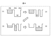
- FIG. 4 shows the photodiode PD of FIG. 2 (hereinafter simply referred to as “PD” as appropriate), the first floating diffusion portion FD1 (hereinafter simply referred to as “FD1” as appropriate), and the second floating diffusion portion FD2 (hereinafter referred to as “PD”).
- FIG. 5 is a potential diagram schematically showing the state of electric charge accumulated in each of the FDs 2. 4 shows the charge states of PD, FD1, and FD2 at time (1) to time (4) indicated by the vertical dotted line in FIG.
- a pixel is selected by applying a pulse through the selection wiring 17 and turning on the selection transistor Tr4.
- the reset transistor Tr2 and the separation transistor Tr5 are turned on, and FD1 and FD2 are reset.
- the reset transistor Tr2 is turned off by falling the pulse of the reset wiring 18 (time (1)).
- the state of charge accumulated in each of PD, FD1, and FD2 is as shown in (1) of FIG. That is, FD1 and FD2 are connected by turning on isolation transistor Tr5. In addition, charges corresponding to the amount of received light are accumulated in the photodiode PD. In this state, the reset signal output to the vertical signal line 9 through the amplification transistor Tr3 is taken into the column signal processing circuit 5 as N2.
- the separation transistor Tr5 is turned off by falling the pulse of the separation wiring 16 (time (2)).
- the transfer transistor Tr1 is turned on and then turned off (time (3)). As a result, charges are transferred from the PD to the FD 1. At this time, if the charge accumulated in the PD is large, the charge remains in the PD.
- the state of charge accumulated in each of PD, FD1, and FD2 is as shown in (3) of FIG. That is, the charge is transferred from the PD to the FD1 by turning on the transfer transistor Tr1. In this example, since the charge accumulated in the PD is large, the charge remains in the PD. In this state, an output signal from the FD 1 output to the vertical signal line 9 through the amplification transistor Tr3 is taken into the column signal processing circuit 5 as S1.
- the state of charge accumulated in each of PD, FD1, and FD2 is as shown in (4) of FIG. That is, FD1 and FD2 are connected by turning on isolation transistor Tr5. Further, since the transfer transistor Tr1 is turned on, charges are transferred from the PD to the FD1 and FD2. In this case, the charge remaining in the PD in (3) of FIG. 4 is also transferred to FD1 and FD2. In this state, the output signals from FD1 and FD2 output to the vertical signal line 9 through the amplification transistor Tr3 are taken into the column signal processing circuit 5 as S2.
- the column signal processing circuit 5 can obtain a pixel signal from which reset noise and the like are removed by taking the difference between the output signal S1 and the reset level signal N1.
- This signal is a signal with a high gain, but an accurate signal cannot be obtained, for example, when the charge accumulated in the PD is large. Therefore, this signal is a pixel signal suitable for low illuminance and will be referred to as a first pixel signal.
- the column signal processing circuit 5 can obtain a pixel signal from which reset noise and the like are removed by taking the difference between the output signal S2 and the reset level signal N2.
- This signal can be obtained as a correct signal, for example, when the charge accumulated in the PD is large or small, but the signal has a low gain. Therefore, this signal is a pixel signal suitable for high illuminance and will be referred to as a second pixel signal.
- the reset level signal N2 in which FD1 and FD2 are connected in the state after reset, and the reset level signal N1 in the state in which FD1 and FD2 are separated are acquired.
- an output signal S1 in a state where FD1 and FD2 are separated and an output signal S1 in a state where FD1 and FD2 are separated are obtained.
- the first pixel signal from which the reset noise is removed is obtained by obtaining the difference between the output signal S1 and the reset level signal N1
- the reset noise is removed by obtaining the difference between the output signal S2 and the reset level signal N2.
- the second pixel signal thus extracted is extracted.
- addition of signals is not required when extracting the first pixel signal or when extracting the second pixel signal.
- the reset level signal N1, the reset level signal N2, the output signal S1, and the output signal S2 are taken into the column signal processing circuit 5.
- the column signal processing circuit 5 includes an ADC that performs AD conversion, a CDS for removing reset noise, and the like. That is, the column signal processing circuit 5 of FIG. 1 is provided with a pixel signal extraction unit having ADC, CDS, etc. corresponding to each vertical signal line 9. *
- FIG. 5 is a block diagram illustrating a configuration example of the pixel signal extraction unit 100 provided in the column signal processing circuit 5.
- an ADC / CDS unit 101 and a sample holder (SH) unit 102 are connected to the vertical signal line 9.
- the pixel signal extraction unit 100 in FIG. 5 holds the reset level signal N2 in the sample holder unit 102 at the time (1) in FIG. 3, that is, the state at (1) in FIG.
- the ADC / CDS unit 101 for example, the reset level signal N1 obtained at the time (2) in FIG. 3, that is, the state at (2) in FIG. 4, and the time (3) in FIG. 3, that is, (3) in FIG.
- the first pixel signal is extracted by taking the difference from the output signal S1 obtained in the state and performing AD conversion.
- the ADC / CDS unit 101 calculates a difference between the reset level signal N2 held in the sample holder unit 102 and the output signal S2 obtained at the time (4) in FIG. 3, that is, the state of (4) in FIG.
- the second pixel signal is extracted by performing AD conversion.
- a first pixel signal or a second pixel signal is selected and output by a selection unit (not shown) provided after the pixel signal extraction unit 100. It is made to be done. For example, if the value of the first pixel signal is smaller than a preset threshold value, the first pixel signal is selected and output; otherwise, the second pixel signal is selected and output. ing.
- FIG. 6 is a block diagram showing another configuration example of the pixel signal extraction unit 100 provided in the column signal processing circuit 5.
- the ADC unit 111 is connected to the vertical signal line 9, and the latch circuits 112-1 to 112-4 are connected to the ADC unit 111. Further, the difference calculation unit 113-1 and the difference calculation unit 113-2 are connected to the latch circuits 112-1 to 112-4.
- the pixel signal extraction unit 100 in FIG. 6 performs AD conversion on the reset level signal N2 by the ADC unit 111 at the time (1) in FIG. 3, that is, the state at (1) in FIG. It is made to hold. Further, at time (2) in FIG. 3, that is, in the state of (2) in FIG. 4, the reset level signal N1 is AD converted by the ADC unit 111 and held in the latch circuit 112-2. Further, at time (3) in FIG. 3, that is, in the state of (3) in FIG. 4, the output signal S1 is AD converted by the ADC unit 111 and held in the latch circuit 112-3. Further, at time (4) in FIG. 3, that is, in the state of (4) in FIG. 4, the output signal S2 is AD-converted by the ADC unit 111 and held in the latch circuit 112-4.
- the difference calculation unit 113-1 calculates the difference between the reset level signal N1 held in the latch circuit 112-2 and the output signal S1 held in the latch circuit 112-3, and extracts the first pixel signal.
- the difference calculation unit 113-2 calculates a difference between the reset level signal N2 held in the latch circuit 112-1 and the output signal S2 held in the latch circuit 112-4, and extracts a second pixel signal. .
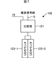
- FIG. 7 is a block diagram showing still another configuration example of the pixel signal extraction unit 100 provided in the column signal processing circuit 5.
- a comparator 121 is connected to the vertical signal line 9 and the ramp signal line 19, and a UD (Up-Down) counter 122-1 and a UD counter 122-2 are connected to the comparator 121.
- the ramp signal is an analog signal whose voltage increases with time from the signal origin.
- the comparator 121 compares the voltages of the vertical signal line 9 and the ramp signal wiring 19 and passes the result to the UD counter 122-1 and the UD counter 122-2.
- the UD counter 122-1 and the UD counter 122-2 perform down-counting and up-counting based on a clock supplied from a PLL circuit (not shown) or the like. More specifically, the UD counter 122-1 and the UD counter 122-2 count up the clock or count down the clock while the voltage of the vertical signal line 9 is higher than the voltage of the ramp signal wiring 19. .
- the count value of the clock when the magnitude relationship between the voltage level of the vertical signal line 9 and the level of the ramp signal is inverted is held.
- the pixel signal extraction unit 100 in FIG. 7 performs the UD counter 122- while the level of the reset level signal N2 is higher than the level of the ramp signal at the time (1) in FIG. 1 up-counts the clock.
- the count value of the clock when the magnitude relationship between the level of the reset level signal N2 and the level of the ramp signal is inverted is held.
- the UD counter 122-2 counts up the clock. The count value of the clock when the magnitude relationship between the level of the reset level signal N1 and the level of the ramp signal is inverted is held.
- the UD counter 122-2 counts down the clock. Then, the count value of the clock when the magnitude relationship between the level of the output signal S1 and the level of the ramp signal is inverted is held. As a result, the held count value corresponds to the difference between the output signal S1 and the reset level signal N1.
- the first pixel signal is extracted by the UD counter 122-2.
- the UD counter 122-1 counts down the clock. Then, the count value of the clock when the magnitude relationship between the level of the output signal S2 and the level of the ramp signal is inverted is held. As a result, the held count value corresponds to the difference between the output signal S2 and the reset level signal N2.
- the second pixel signal is extracted by the UD counter 122-1.
- the present technology it is possible to extract the first pixel signal and the second pixel signal from each pixel by driving the pixel 2 by a control signal as shown in FIG.
- the reset level signal N2 and the reset level signal N1 are acquired before the charge is transferred from the PD to the FD1 and FD2.
- an accurate reset level signal can be obtained.
- step S21 FD1 and FD2 are connected and reset. At this time, by applying a pulse through the reset wiring 18 and the separation wiring 16, the reset transistor Tr2 and the separation transistor Tr5 are turned on, and reset is performed in a state where the FD1 and FD2 are connected. The reset transistor Tr2 is turned off thereafter.
- step S22 the reset level signal N2 is acquired and held.
- the state of charge accumulated in each of PD, FD1, and FD2 is as shown in (1) of FIG. That is, FD1 and FD2 are connected by turning on isolation transistor Tr5. In addition, charges corresponding to the amount of received light are accumulated in the photodiode PD.
- the reset level signal output to the vertical signal line 9 through the amplification transistor Tr3 is taken into the column signal processing circuit 5 as N2.
- the reset level signal N2 is held in the pixel signal extraction unit 100 described above with reference to FIGS.
- step S23 FD1 and FD2 are separated. At this time, when the pulse of the separation wiring 16 falls, the separation transistor Tr5 is turned off and the FD1 and the FD2 are separated.
- step S24 the reset level signal N1 is acquired and held.
- the state of charge accumulated in each of PD, FD1, and FD2 is as shown in (2) of FIG. That is, FD1 and FD2 are separated by turning off separation transistor Tr5. In addition, charges corresponding to the amount of received light are accumulated in the photodiode PD.
- the reset level signal output to the vertical signal line 9 through the amplification transistor Tr3 is taken into the column signal processing circuit 5 as N1.
- the reset level signal N1 is held in the pixel signal extraction unit 100.
- step S25 charge is transferred from the PD.
- the transfer transistor Tr1 is turned on and then turned off.
- charges are transferred from the PD to the FD 1.
- the charge remains in the PD.
- step S26 the output signal S1 is acquired.
- the state of charge accumulated in each of PD, FD1, and FD2 is as shown in (3) of FIG. That is, the charge is transferred from the PD to the FD1 by turning on the transfer transistor Tr1. In this example, since the charge accumulated in the PD is large, the charge remains in the PD. In this state, the output signal from the FD 1 output to the vertical signal line 9 through the amplification transistor Tr3 is taken into the column signal processing circuit 5 as S1.
- step S27 the pixel signal extraction unit 100 extracts the first pixel signal by calculating the difference between the reset level signal N1 acquired in step S24 and the output signal S1 acquired in step S26.
- step S28 FD1 and FD2 are connected again.
- the separation transistor Tr5 is turned on, and FD1 and FD2 are connected again.
- step S29 charge is transferred from the PD.
- step S29 charge is transferred from the PD.
- a pulse of the transfer wiring 15 to turn on the transfer transistor Tr1, and then turning it off, charges are transferred from the PD to the FD1 and FD2.
- step S30 the output signal S2 is acquired.
- step S31 the pixel signal extraction unit 100 extracts the second pixel signal by calculating the difference between the reset level signal N2 acquired in step S22 and the output signal S2 acquired in step S30.
- step S32 either the first pixel signal extracted in the process of step S27 or the second pixel signal extracted in the process of step S31 is selected and output as the pixel signal of the pixel.
- either the first pixel signal or the second pixel signal is selected by, for example, a selection unit (not shown) provided after the pixel signal extraction unit 100. Is output. For example, if the value of the first pixel signal is smaller than a preset threshold value, the first pixel signal is selected and output; otherwise, the second pixel signal is selected and output.
- both the first pixel signal and the second pixel signal may be output, or the first pixel signal and the second pixel signal are combined into one signal and output. May be.
- the same driving can be performed by reading three times until no charge remains in the PD. That is, the reset level signal N3 with the FD1 to FD3 connected is read, and the reset level signal N2 and the reset level signal N1 are read in order. Thereafter, the output signal S1, the output signal S2, and the output signal S3 are read in order. Then, the reset noise is removed by the difference between N3 and S3, the reset noise is removed by the difference between N2 and S2, and the reset noise is removed by the difference between N1 and S1.
- the present technology can be applied to a case where the floating diffusion portion is divided into four or more.
- the present technology is not limited to application to a solid-state imaging device such as a CMOS image sensor. That is, the present technology is applied to an image capturing unit (photoelectric conversion unit) such as an imaging device such as a digital still camera or a video camera, a portable terminal device having an imaging function, or a copying machine using a solid-state imaging device as an image reading unit.
- the present invention can be applied to all electronic devices using a solid-state image sensor.
- the solid-state image sensor may be formed as a single chip, or may be a form in which a plurality of chips are stacked or adjacent to each other, or the image pickup unit and the signal processing unit or optical system are packaged together. It may be in the form of a module having a captured imaging function.
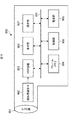
- FIG. 9 is a block diagram illustrating a configuration example of an imaging apparatus as an electronic apparatus to which the present technology is applied.
- the imaging apparatus 600 includes an optical unit 601 including a lens group, a solid-state imaging device (imaging device) 602 in which each configuration of the pixel 2 described above is employed, and a DSP circuit 603 that is a camera signal processing circuit.
- the imaging apparatus 600 also includes a frame memory 604, a display unit 605, a recording unit 606, an operation unit 607, and a power supply unit 608.
- the DSP circuit 603, the frame memory 604, the display unit 605, the recording unit 606, the operation unit 607, and the power supply unit 608 are connected to each other via a bus line 609.
- the optical unit 601 takes in incident light (image light) from a subject and forms an image on the imaging surface of the solid-state imaging device 602.
- the solid-state imaging device 602 converts the amount of incident light imaged on the imaging surface by the optical unit 601 into an electrical signal for each pixel and outputs the electrical signal as a pixel signal.
- a solid-state imaging device such as the CMOS image sensor 1 according to the above-described embodiment, that is, a solid-state imaging device capable of realizing imaging without distortion by global exposure can be used.
- the display unit 605 includes a panel type display device such as a liquid crystal panel or an organic EL (Electro Luminescence) panel, and displays a moving image or a still image captured by the solid-state imaging device 602.
- the recording unit 606 records a moving image or a still image captured by the solid-state imaging device 602 on a recording medium such as a video tape or a DVD (Digital Versatile Disk).
- the operation unit 607 issues operation commands for various functions of the imaging apparatus 600 under the operation of the user.
- the power supply unit 608 appropriately supplies various power sources serving as operation power sources for the DSP circuit 603, the frame memory 604, the display unit 605, the recording unit 606, and the operation unit 607 to these supply targets.
- the second pixel signal can be extracted without performing signal addition. Since the reset noise can be accurately removed also when extracting the pixel signal, the captured image is captured by the imaging device 600 such as a video camera, a digital still camera, or a camera module for a mobile device such as a mobile phone. Image quality can be improved.
- the present invention is applied to a CMOS image sensor in which unit pixels that detect signal charges corresponding to the amount of visible light as physical quantities are arranged in a matrix has been described as an example.
- the present technology is not limited to application to a CMOS image sensor, and can be applied to all column-type solid-state imaging devices in which a column processing unit is arranged for each pixel column of a pixel array unit.
- the present technology is not limited to application to a solid-state imaging device that detects the distribution of the amount of incident light of visible light and captures it as an image, but a solid-state that captures the distribution of the incident amount of infrared rays, X-rays, or particles as an image.
- solid-state imaging devices physical quantity distribution detection devices
- fingerprint detection sensors that detect the distribution of other physical quantities such as pressure and capacitance, and take images as images.
- this technology can also take the following structures.
- the pixel is A photoelectric conversion unit that performs photoelectric conversion;
- a transfer unit that transfers charges from the photoelectric conversion unit;
- a plurality of detection units for detecting the charges transferred by the transfer unit;
- a reset unit for resetting the plurality of detection units;
- a connection separation control unit for controlling connection or separation of the plurality of detection units;
- An output unit that outputs a signal corresponding to the potential of the detection unit;
- the output unit is In a state where the connection separation control unit is connected to the plurality of detection units, a connection state reset level signal and a connection state output signal are output, In the state where the plurality of detection units are separated by the connection separation control unit, a separation state reset level signal and a separation state output signal are output, A first pixel signal is generated by a difference between the connection state reset level signal and the connection state output signal, and a second pixel signal is generated by a difference between the separation state reset level signal and the separation state output signal
- Solid-state image sensor (2) Based on the level of the first pixel signal, select either the first pixel signal or the second pixel signal, The solid-state imaging device according to (1), wherein the selected first pixel signal or the second pixel signal is output as a pixel signal related to the pixel. (3) The pixels are arranged in a two-dimensional matrix; The solid-state imaging device according to (1) or (2), wherein a difference between the signals output from the output unit is calculated by a difference calculation unit arranged corresponding to a column in the pixel.
- the pixels are arranged in a two-dimensional matrix; The pixels are arranged corresponding to the columns, The solid-state imaging device according to any one of (1) to (3), wherein a difference between signals output from the output unit is calculated by a difference calculation unit configured by a CDS (Correlated Double Sampling) circuit having a sample holder.
- the pixels are arranged in a two-dimensional matrix; The pixels are arranged corresponding to the columns, The difference between the signals output from the output unit is obtained by a difference calculation unit having a latch circuit that holds the connection state reset level signal, the separation state reset level signal, the separation state output signal, and the connection state output signal, respectively.
- the solid-state imaging device according to any one of (1) to (3).
- the pixels are arranged in a two-dimensional matrix; The pixels are arranged corresponding to the columns, A first up / down counter that counts the level of the connection state reset level signal in one direction and counts the level of the connection state output signal in the other direction, and the level of the separation state reset level signal in one direction A difference of the signals output from the output unit is calculated by a difference calculation unit having a second up / down counter that counts and counts the level of the separated state output signal in the other direction. (1) to (3 ).
- the pixel is A photoelectric conversion unit that performs photoelectric conversion;
- a transfer unit that transfers charges from the photoelectric conversion unit;
- a plurality of detection units for detecting the charges transferred by the transfer unit;
- a reset unit for resetting the plurality of detection units;
- a connection separation control unit for controlling connection or separation of the plurality of detection units;
- a solid-state imaging device driving method comprising: an output unit that outputs a signal corresponding to the potential of the detection unit;
- the output unit is In a state where the connection separation control unit is connected to the plurality of detection units, a connection state reset level signal and a connection state output signal are output, In the state where the plurality of detection units are separated by the connection separation control unit, a separation state reset level signal and a separation state output signal are output,
- a first pixel signal is generated by a difference between the connection state reset level signal and the connection state output signal
- a second pixel signal is generated by a difference
- the pixel is A photoelectric conversion unit that performs photoelectric conversion;
- a transfer unit that transfers charges from the photoelectric conversion unit;
- a plurality of detection units for detecting the charges transferred by the transfer unit;
- a reset unit for resetting the plurality of detection units;
- a connection separation control unit for controlling connection or separation of the plurality of detection units;
- An output unit that outputs a signal corresponding to the potential of the detection unit;
- the output unit is In a state where the connection separation control unit is connected to the plurality of detection units, a connection state reset level signal and a connection state output signal are output, In the state where the plurality of detection units are separated by the connection separation control unit, a separation state reset level signal and a separation state output signal are output, A first pixel signal is generated by a difference between the connection state reset level signal and the connection state output signal, and a second pixel signal is generated by a difference between the separation state reset level signal and the separation state output signal
- CMOS image sensor 1 CMOS image sensor, 2 pixels, 3 pixel area, 4 vertical drive circuit, 5 column processing circuit, 7 output circuit, 8 control circuit, 9 vertical signal line, 11 semiconductor substrate, 12 input / output terminal, 100 pixel signal extraction unit, 101 ADC / CDS section, 102 sample holder section, 111 ADC section, 112-1 to 112-4 latch circuit, 113-1, 113-2 difference calculation section, 121 comparator, 122-1, 122-2 up / down counter
Abstract
Description
複数の画素が配列された画素領域を有し、
前記画素は、
光電変換を行う光電変換部と、
前記光電変換部から電荷を転送する転送部と、
前記転送部により転送された電荷を検出する複数の検出部と、
前記複数の検出部をリセットするリセット部と、
前記複数の検出部の接続または分離を制御する接続分離制御部と、
前記検出部の電位に対応する信号を出力する出力部とを備え、
前記出力部は、
前記接続分離制御部が前記複数の検出部を接続した状態において、接続状態リセットレベル信号及び接続状態出力信号を出力し、
前記接続分離制御部が前記複数の検出部が分離した状態において、分離状態リセットレベル信号及び分離状態出力信号を出力し、
前記接続状態リセットレベル信号と前記接続状態出力信号との差分により第1の画素信号が生成され、前記分離状態リセットレベル信号と前記分離状態出力信号との差分により第2の画素信号が生成される
固体撮像素子。
(2)
前記第1の画素信号のレベルに基づいて、前記第1の画素信号、または、前記第2の画素信号のいずれかを選択し、
前記選択された前記第1の画素信号、または、前記第2の画素信号を当該画素に係る画素信号として出力する
(1)に記載の固体撮像素子。
(3)
前記画素が2次元行列状に配列され、
前記画素に列に対応して配置されている差分演算部によって、前記出力部から出力された信号の差分が演算される
(1)または(2)記載の固体撮像素子。
(4)
前記画素が2次元行列状に配列され、
前記画素に列に対応して配置され、
サンプルホルダを有するCDS(Correlated Double Sampling)回路により構成される差分演算部によって、前記出力部から出力された信号の差分が演算される
(1)乃至(3)のいずれかに記載の固体撮像素子
(5)
前記画素が2次元行列状に配列され、
前記画素に列に対応して配置され、
前記接続状態リセットレベル信号、前記分離状態リセットレベル信号、前記分離状態出力信号、および前記接続状態出力信号をそれぞれ保持するラッチ回路を有する差分演算部によって、前記出力部から出力された信号の差分が演算される
(1)乃至(3)のいずれかに記載の固体撮像素子。
(6)
前記画素が2次元行列状に配列され、
前記画素に列に対応して配置され、
前記接続状態リセットレベル信号のレベルを一方向にカウントするとともに、前記接続状態出力信号のレベルを他方向にカウントする第1のアップダウンカウンタ、および、前記分離状態リセットレベル信号のレベルを一方向にカウントするとともに、前記分離状態出力信号のレベルを他方向にカウントする第2のアップダウンカウンタを有する差分演算部によって、前記出力部から出力された信号の差分が演算される
(1)乃至(3)のいずれかに記載の固体撮像素子。
(7)
複数の画素が配列された画素領域を有し、
前記画素は、
光電変換を行う光電変換部と、
前記光電変換部から電荷を転送する転送部と、
前記転送部により転送された電荷を検出する複数の検出部と、
前記複数の検出部をリセットするリセット部と、
前記複数の検出部の接続または分離を制御する接続分離制御部と、
前記検出部の電位に対応する信号を出力する出力部とを備える固体撮像素子の駆動方法であって、
前記出力部が、
前記接続分離制御部が前記複数の検出部を接続した状態において、接続状態リセットレベル信号及び接続状態出力信号を出力し、
前記接続分離制御部が前記複数の検出部が分離した状態において、分離状態リセットレベル信号及び分離状態出力信号を出力し、
前記接続状態リセットレベル信号と前記接続状態出力信号との差分により第1の画素信号が生成され、前記分離状態リセットレベル信号と前記分離状態出力信号との差分により第2の画素信号が生成される
駆動方法。
(8)
複数の画素が配列された画素領域を有し、
前記画素は、
光電変換を行う光電変換部と、
前記光電変換部から電荷を転送する転送部と、
前記転送部により転送された電荷を検出する複数の検出部と、
前記複数の検出部をリセットするリセット部と、
前記複数の検出部の接続または分離を制御する接続分離制御部と、
前記検出部の電位に対応する信号を出力する出力部とを有し、
前記出力部は、
前記接続分離制御部が前記複数の検出部を接続した状態において、接続状態リセットレベル信号及び接続状態出力信号を出力し、
前記接続分離制御部が前記複数の検出部が分離した状態において、分離状態リセットレベル信号及び分離状態出力信号を出力し、
前記接続状態リセットレベル信号と前記接続状態出力信号との差分により第1の画素信号が生成され、前記分離状態リセットレベル信号と前記分離状態出力信号との差分により第2の画素信号が生成される固体撮像素子を備える
電子機器。
Claims (8)
- 複数の画素が配列された画素領域を有し、
前記画素は、
光電変換を行う光電変換部と、
前記光電変換部から電荷を転送する転送部と、
前記転送部により転送された電荷を検出する複数の検出部と、
前記複数の検出部をリセットするリセット部と、
前記複数の検出部の接続または分離を制御する接続分離制御部と、
前記検出部の電位に対応する信号を出力する出力部とを備え、
前記出力部は、
前記接続分離制御部が前記複数の検出部を接続した状態において、接続状態リセットレベル信号及び接続状態出力信号を出力し、
前記接続分離制御部が前記複数の検出部が分離した状態において、分離状態リセットレベル信号及び分離状態出力信号を出力し、
前記接続状態リセットレベル信号と前記接続状態出力信号との差分により第1の画素信号が生成され、前記分離状態リセットレベル信号と前記分離状態出力信号との差分により第2の画素信号が生成される
固体撮像素子。 - 前記第1の画素信号のレベルに基づいて、前記第1の画素信号、または、前記第2の画素信号のいずれかを選択し、
前記選択された前記第1の画素信号、または、前記第2の画素信号を当該画素に係る画素信号として出力する
請求項1に記載の固体撮像素子。 - 前記画素が2次元行列状に配列され、
前記画素に列に対応して配置されている差分演算部によって、前記出力部から出力された信号の差分が演算される
請求項1記載の固体撮像素子。 - 前記画素が2次元行列状に配列され、
前記画素に列に対応して配置され、
サンプルホルダを有するCDS(Correlated Double Sampling)回路により構成される差分演算部によって、前記出力部から出力された信号の差分が演算される
請求項1に記載の固体撮像素子。 - 前記画素が2次元行列状に配列され、
前記画素に列に対応して配置され、
前記接続状態リセットレベル信号、前記分離状態リセットレベル信号、前記分離状態出力信号、および前記接続状態出力信号をそれぞれ保持するラッチ回路を有する差分演算部によって、前記出力部から出力された信号の差分が演算される
請求項1に記載の固体撮像素子。 - 前記画素が2次元行列状に配列され、
前記画素に列に対応して配置され、
前記接続状態リセットレベル信号のレベルを一方向にカウントするとともに、前記接続状態出力信号のレベルを他方向にカウントする第1のアップダウンカウンタ、および、前記分離状態リセットレベル信号のレベルを一方向にカウントするとともに、前記分離状態出力信号のレベルを他方向にカウントする第2のアップダウンカウンタを有する差分演算部によって、前記出力部から出力された信号の差分が演算される
請求項1に記載の固体撮像素子。 - 複数の画素が配列された画素領域を有し、
前記画素は、
光電変換を行う光電変換部と、
前記光電変換部から電荷を転送する転送部と、
前記転送部により転送された電荷を検出する複数の検出部と、
前記複数の検出部をリセットするリセット部と、
前記複数の検出部の接続または分離を制御する接続分離制御部と、
前記検出部の電位に対応する信号を出力する出力部とを備える固体撮像素子の駆動方法であって、
前記出力部が、
前記接続分離制御部が前記複数の検出部を接続した状態において、接続状態リセットレベル信号及び接続状態出力信号を出力し、
前記接続分離制御部が前記複数の検出部が分離した状態において、分離状態リセットレベル信号及び分離状態出力信号を出力し、
前記接続状態リセットレベル信号と前記接続状態出力信号との差分により第1の画素信号が生成され、前記分離状態リセットレベル信号と前記分離状態出力信号との差分により第2の画素信号が生成される
駆動方法。 - 複数の画素が配列された画素領域を有し、
前記画素は、
光電変換を行う光電変換部と、
前記光電変換部から電荷を転送する転送部と、
前記転送部により転送された電荷を検出する複数の検出部と、
前記複数の検出部をリセットするリセット部と、
前記複数の検出部の接続または分離を制御する接続分離制御部と、
前記検出部の電位に対応する信号を出力する出力部とを有し、
前記出力部は、
前記接続分離制御部が前記複数の検出部を接続した状態において、接続状態リセットレベル信号及び接続状態出力信号を出力し、
前記接続分離制御部が前記複数の検出部が分離した状態において、分離状態リセットレベル信号及び分離状態出力信号を出力し、
前記接続状態リセットレベル信号と前記接続状態出力信号との差分により第1の画素信号が生成され、前記分離状態リセットレベル信号と前記分離状態出力信号との差分により第2の画素信号が生成される固体撮像素子を備える
電子機器。
Priority Applications (5)
| Application Number | Priority Date | Filing Date | Title |
|---|---|---|---|
| EP13741593.1A EP2809065B1 (en) | 2012-01-27 | 2013-01-11 | Solid-state image sensor, driving method therefor, and electronic device |
| KR1020147019734A KR102013001B1 (ko) | 2012-01-27 | 2013-01-11 | 고체 촬상 소자와 구동 방법 및 전자 기기 |
| JP2013555217A JP6120091B2 (ja) | 2012-01-27 | 2013-01-11 | 固体撮像素子および駆動方法、並びに電子機器 |
| CN201380011297.5A CN104137536B (zh) | 2012-01-27 | 2013-01-11 | 固态成像元件及其驱动方法以及电子设备 |
| US14/371,615 US10136081B2 (en) | 2012-01-27 | 2013-01-11 | Solid-state imaging element with latch circuits and electronic device equipped with the same |
Applications Claiming Priority (2)
| Application Number | Priority Date | Filing Date | Title |
|---|---|---|---|
| JP2012-014859 | 2012-01-27 | ||
| JP2012014859 | 2012-01-27 |
Publications (1)
| Publication Number | Publication Date |
|---|---|
| WO2013111629A1 true WO2013111629A1 (ja) | 2013-08-01 |
Family
ID=48873351
Family Applications (1)
| Application Number | Title | Priority Date | Filing Date |
|---|---|---|---|
| PCT/JP2013/050407 WO2013111629A1 (ja) | 2012-01-27 | 2013-01-11 | 固体撮像素子および駆動方法、並びに電子機器 |
Country Status (7)
| Country | Link |
|---|---|
| US (1) | US10136081B2 (ja) |
| EP (1) | EP2809065B1 (ja) |
| JP (1) | JP6120091B2 (ja) |
| KR (1) | KR102013001B1 (ja) |
| CN (1) | CN104137536B (ja) |
| TW (1) | TWI533699B (ja) |
| WO (1) | WO2013111629A1 (ja) |
Cited By (5)
| Publication number | Priority date | Publication date | Assignee | Title |
|---|---|---|---|---|
| WO2016152184A1 (ja) * | 2015-03-25 | 2016-09-29 | ソニー株式会社 | 固体撮像装置および固体撮像装置の駆動方法 |
| WO2018110303A1 (ja) * | 2016-12-14 | 2018-06-21 | ソニーセミコンダクタソリューションズ株式会社 | 固体撮像素子および電子機器 |
| WO2019017217A1 (ja) * | 2017-07-21 | 2019-01-24 | ソニーセミコンダクタソリューションズ株式会社 | 固体撮像素子およびその制御方法、並びに電子機器 |
| WO2019193801A1 (ja) * | 2018-04-04 | 2019-10-10 | ソニーセミコンダクタソリューションズ株式会社 | 固体撮像素子、電子機器および固体撮像素子の制御方法 |
| EP2890117B1 (en) * | 2013-12-26 | 2020-11-18 | IMEC vzw | Improvements in or relating to imaging sensors |
Families Citing this family (9)
| Publication number | Priority date | Publication date | Assignee | Title |
|---|---|---|---|---|
| TWI533699B (zh) * | 2012-01-27 | 2016-05-11 | Sony Corp | A solid-state imaging element and a driving method, and an electronic device |
| JP2016012905A (ja) * | 2014-06-02 | 2016-01-21 | ソニー株式会社 | 撮像素子、撮像方法、および電子機器 |
| JP2018186398A (ja) * | 2017-04-26 | 2018-11-22 | ソニーセミコンダクタソリューションズ株式会社 | 固体撮像装置、および電子機器 |
| US10103193B1 (en) * | 2017-08-03 | 2018-10-16 | Omnivision Technologies, Inc. | Apparatus and method for low dark current floating diffusion |
| GB2567903A (en) | 2017-10-27 | 2019-05-01 | Cirrus Logic Int Semiconductor Ltd | Socket monitoring |
| JP7146424B2 (ja) | 2018-03-19 | 2022-10-04 | キヤノン株式会社 | 光電変換装置及び撮像システム |
| CN109040631A (zh) * | 2018-08-01 | 2018-12-18 | 西北核技术研究所 | 多采样cmos图像传感器像元结构及其超高速图像获取方法 |
| EP3655992B1 (en) * | 2018-10-09 | 2021-08-18 | Shenzhen Goodix Technology Co., Ltd. | Image sensor with dynamic charge-domain sampling |
| TWI756098B (zh) * | 2021-04-07 | 2022-02-21 | 神泰科技股份有限公司 | 指紋畫素單元、指紋感測裝置及整合積體電路 |
Citations (5)
| Publication number | Priority date | Publication date | Assignee | Title |
|---|---|---|---|---|
| JPS6367976A (ja) | 1986-09-10 | 1988-03-26 | Toshiba Corp | 固体撮像装置 |
| JP2000165754A (ja) * | 1998-11-27 | 2000-06-16 | Canon Inc | 固体撮像装置および固体撮像装置の信号読出し方法 |
| JP2005083790A (ja) | 2003-09-05 | 2005-03-31 | Tamron Co Ltd | レーザ水準器 |
| JP2007516654A (ja) * | 2003-06-11 | 2007-06-21 | マイクロン テクノロジー インコーポレイテッド | 2段階変換利得イメージャ |
| JP2009505498A (ja) | 2005-08-10 | 2009-02-05 | マイクロン テクノロジー, インク. | 二重変換利得ゲートを介してリセットされるイメージピクセル |
Family Cites Families (15)
| Publication number | Priority date | Publication date | Assignee | Title |
|---|---|---|---|---|
| US6115066A (en) * | 1997-06-12 | 2000-09-05 | International Business Machines Corporation | Image sensor with direct digital correlated sampling |
| US6850278B1 (en) | 1998-11-27 | 2005-02-01 | Canon Kabushiki Kaisha | Solid-state image pickup apparatus |
| US6519211B1 (en) | 1999-04-01 | 2003-02-11 | Matsushita Electric Industrial Co., Ltd. | Magneto-optical recording medium having magnetic domain shrinks and disappears |
| CN100499146C (zh) * | 2004-02-27 | 2009-06-10 | 国立大学法人东北大学 | 固体摄像装置及其工作方法、线传感器、光传感器 |
| US7518143B2 (en) * | 2004-02-27 | 2009-04-14 | National University Corporation Tohoku University | Solid-state imaging device, line sensor and optical sensor and method of operating solid-state imaging device |
| JP4289206B2 (ja) * | 2004-04-26 | 2009-07-01 | ソニー株式会社 | カウンタ回路 |
| JP2006019343A (ja) * | 2004-06-30 | 2006-01-19 | Pentax Corp | 固体撮像素子 |
| JP4691930B2 (ja) | 2004-09-10 | 2011-06-01 | ソニー株式会社 | 物理情報取得方法および物理情報取得装置、並びに物理量分布検知の半導体装置、プログラム、および撮像モジュール |
| JP2008205639A (ja) | 2007-02-16 | 2008-09-04 | Texas Instr Japan Ltd | 固体撮像装置及びその動作方法 |
| JP4389981B2 (ja) * | 2007-08-06 | 2009-12-24 | ソニー株式会社 | 固体撮像装置、固体撮像装置のアナログ−デジタル変換方法および撮像装置 |
| JP4743227B2 (ja) * | 2008-05-12 | 2011-08-10 | ソニー株式会社 | Ad変換方法およびad変換装置、並びに物理量分布検知の半導体装置および電子機器 |
| GB2477083A (en) * | 2010-01-13 | 2011-07-27 | Cmosis Nv | Pixel structure with multiple transfer gates to improve dynamic range |
| JP5552858B2 (ja) * | 2010-03-26 | 2014-07-16 | ソニー株式会社 | 固体撮像装置、固体撮像装置の駆動方法、及び、電子機器 |
| JP5664175B2 (ja) * | 2010-11-29 | 2015-02-04 | ソニー株式会社 | 固体撮像装置とその駆動方法、及び電子機器 |
| TWI533699B (zh) * | 2012-01-27 | 2016-05-11 | Sony Corp | A solid-state imaging element and a driving method, and an electronic device |
-
2012
- 2012-12-28 TW TW101150785A patent/TWI533699B/zh not_active IP Right Cessation
-
2013
- 2013-01-11 JP JP2013555217A patent/JP6120091B2/ja active Active
- 2013-01-11 CN CN201380011297.5A patent/CN104137536B/zh active Active
- 2013-01-11 WO PCT/JP2013/050407 patent/WO2013111629A1/ja active Application Filing
- 2013-01-11 US US14/371,615 patent/US10136081B2/en active Active
- 2013-01-11 KR KR1020147019734A patent/KR102013001B1/ko active IP Right Grant
- 2013-01-11 EP EP13741593.1A patent/EP2809065B1/en active Active
Patent Citations (5)
| Publication number | Priority date | Publication date | Assignee | Title |
|---|---|---|---|---|
| JPS6367976A (ja) | 1986-09-10 | 1988-03-26 | Toshiba Corp | 固体撮像装置 |
| JP2000165754A (ja) * | 1998-11-27 | 2000-06-16 | Canon Inc | 固体撮像装置および固体撮像装置の信号読出し方法 |
| JP2007516654A (ja) * | 2003-06-11 | 2007-06-21 | マイクロン テクノロジー インコーポレイテッド | 2段階変換利得イメージャ |
| JP2005083790A (ja) | 2003-09-05 | 2005-03-31 | Tamron Co Ltd | レーザ水準器 |
| JP2009505498A (ja) | 2005-08-10 | 2009-02-05 | マイクロン テクノロジー, インク. | 二重変換利得ゲートを介してリセットされるイメージピクセル |
Non-Patent Citations (1)
| Title |
|---|
| See also references of EP2809065A4 |
Cited By (12)
| Publication number | Priority date | Publication date | Assignee | Title |
|---|---|---|---|---|
| EP2890117B1 (en) * | 2013-12-26 | 2020-11-18 | IMEC vzw | Improvements in or relating to imaging sensors |
| WO2016152184A1 (ja) * | 2015-03-25 | 2016-09-29 | ソニー株式会社 | 固体撮像装置および固体撮像装置の駆動方法 |
| JPWO2016152184A1 (ja) * | 2015-03-25 | 2018-01-18 | ソニー株式会社 | 固体撮像装置および固体撮像装置の駆動方法 |
| US10205893B2 (en) | 2015-03-25 | 2019-02-12 | Sony Corporation | Solid-state imaging device and driving method of solid-state imaging device |
| WO2018110303A1 (ja) * | 2016-12-14 | 2018-06-21 | ソニーセミコンダクタソリューションズ株式会社 | 固体撮像素子および電子機器 |
| JPWO2018110303A1 (ja) * | 2016-12-14 | 2019-10-24 | ソニーセミコンダクタソリューションズ株式会社 | 固体撮像素子および電子機器 |
| US10868056B2 (en) | 2016-12-14 | 2020-12-15 | Sony Semiconductor Solutions Corporation | Solid-state imaging element and electronic apparatus |
| JP7155012B2 (ja) | 2016-12-14 | 2022-10-18 | ソニーセミコンダクタソリューションズ株式会社 | 固体撮像素子および電子機器 |
| WO2019017217A1 (ja) * | 2017-07-21 | 2019-01-24 | ソニーセミコンダクタソリューションズ株式会社 | 固体撮像素子およびその制御方法、並びに電子機器 |
| US11218658B2 (en) | 2017-07-21 | 2022-01-04 | Sony Semiconductor Solutions Corporation | Solid-state imaging device, method of controlling the solid-state imaging device, and electronic apparatus to generate high dynamic range image |
| WO2019193801A1 (ja) * | 2018-04-04 | 2019-10-10 | ソニーセミコンダクタソリューションズ株式会社 | 固体撮像素子、電子機器および固体撮像素子の制御方法 |
| US11503240B2 (en) | 2018-04-04 | 2022-11-15 | Sony Semiconductor Solutions Corporation | Solid-state image pickup element, electronic apparatus, and method of controlling solid-state image pickup element |
Also Published As
| Publication number | Publication date |
|---|---|
| JP6120091B2 (ja) | 2017-04-26 |
| EP2809065A1 (en) | 2014-12-03 |
| EP2809065A4 (en) | 2015-09-23 |
| CN104137536B (zh) | 2018-06-22 |
| US20140327802A1 (en) | 2014-11-06 |
| TW201338526A (zh) | 2013-09-16 |
| CN104137536A (zh) | 2014-11-05 |
| KR20140119028A (ko) | 2014-10-08 |
| US10136081B2 (en) | 2018-11-20 |
| TWI533699B (zh) | 2016-05-11 |
| KR102013001B1 (ko) | 2019-08-21 |
| JPWO2013111629A1 (ja) | 2015-05-11 |
| EP2809065B1 (en) | 2021-03-03 |
Similar Documents
| Publication | Publication Date | Title |
|---|---|---|
| JP6120091B2 (ja) | 固体撮像素子および駆動方法、並びに電子機器 | |
| US10044947B2 (en) | Electronic apparatus and driving method therefor | |
| JP5458582B2 (ja) | 固体撮像装置、固体撮像装置の駆動方法および電子機器 | |
| JP5552858B2 (ja) | 固体撮像装置、固体撮像装置の駆動方法、及び、電子機器 | |
| JP5664175B2 (ja) | 固体撮像装置とその駆動方法、及び電子機器 | |
| US9432602B2 (en) | Solid-state imaging device, driving method, and electronic device | |
| US9402038B2 (en) | Solid-state imaging device and method of driving comprising a first and second accumulation sections for transferring charges exceeding the saturation amount | |
| JP2011229120A (ja) | 固体撮像装置、固体撮像装置の信号処理方法、及び、電子機器 | |
| JP2012129799A (ja) | 固体撮像素子および駆動方法、並びに電子機器 | |
| JP2013225734A (ja) | 固体撮像装置および電子機器 | |
| JP2013162148A (ja) | 個体撮像装置および駆動方法、並びに電子機器 | |
| TWI788972B (zh) | 暗電流校準方法及相關像素電路 | |
| JP2014016382A (ja) | 固体撮像装置、電子機器、および画素読み出し方法 | |
| JP2014078869A (ja) | 固体撮像素子および撮像装置並びに固体撮像素子の駆動制御方法 | |
| JP2013197697A (ja) | 固体撮像装置及び電子機器 | |
| JP5306906B2 (ja) | 固体撮像装置、固体撮像装置の駆動方法および電子機器 | |
| JP5402993B2 (ja) | 固体撮像装置、固体撮像装置の駆動方法および電子機器 |
Legal Events
| Date | Code | Title | Description |
|---|---|---|---|
| 121 | Ep: the epo has been informed by wipo that ep was designated in this application |
Ref document number: 13741593 Country of ref document: EP Kind code of ref document: A1 |
|
| ENP | Entry into the national phase |
Ref document number: 2013555217 Country of ref document: JP Kind code of ref document: A |
|
| WWE | Wipo information: entry into national phase |
Ref document number: 2013741593 Country of ref document: EP |
|
| WWE | Wipo information: entry into national phase |
Ref document number: 14371615 Country of ref document: US |
|
| ENP | Entry into the national phase |
Ref document number: 20147019734 Country of ref document: KR Kind code of ref document: A |
|
| NENP | Non-entry into the national phase |
Ref country code: DE |