WO2013089030A1 - 表示装置、及びテレビ受信装置 - Google Patents
表示装置、及びテレビ受信装置 Download PDFInfo
- Publication number
- WO2013089030A1 WO2013089030A1 PCT/JP2012/081772 JP2012081772W WO2013089030A1 WO 2013089030 A1 WO2013089030 A1 WO 2013089030A1 JP 2012081772 W JP2012081772 W JP 2012081772W WO 2013089030 A1 WO2013089030 A1 WO 2013089030A1
- Authority
- WO
- WIPO (PCT)
- Prior art keywords
- frame
- liquid crystal
- display device
- substrate
- guide plate
- Prior art date
- Legal status (The legal status is an assumption and is not a legal conclusion. Google has not performed a legal analysis and makes no representation as to the accuracy of the status listed.)
- Ceased
Links
Images


Classifications
-
- G—PHYSICS
- G02—OPTICS
- G02F—OPTICAL DEVICES OR ARRANGEMENTS FOR THE CONTROL OF LIGHT BY MODIFICATION OF THE OPTICAL PROPERTIES OF THE MEDIA OF THE ELEMENTS INVOLVED THEREIN; NON-LINEAR OPTICS; FREQUENCY-CHANGING OF LIGHT; OPTICAL LOGIC ELEMENTS; OPTICAL ANALOGUE/DIGITAL CONVERTERS
- G02F1/00—Devices or arrangements for the control of the intensity, colour, phase, polarisation or direction of light arriving from an independent light source, e.g. switching, gating or modulating; Non-linear optics
- G02F1/01—Devices or arrangements for the control of the intensity, colour, phase, polarisation or direction of light arriving from an independent light source, e.g. switching, gating or modulating; Non-linear optics for the control of the intensity, phase, polarisation or colour
- G02F1/13—Devices or arrangements for the control of the intensity, colour, phase, polarisation or direction of light arriving from an independent light source, e.g. switching, gating or modulating; Non-linear optics for the control of the intensity, phase, polarisation or colour based on liquid crystals, e.g. single liquid crystal display cells
- G02F1/133—Constructional arrangements; Operation of liquid crystal cells; Circuit arrangements
- G02F1/1333—Constructional arrangements; Manufacturing methods
- G02F1/133308—Support structures for LCD panels, e.g. frames or bezels
-
- G—PHYSICS
- G02—OPTICS
- G02F—OPTICAL DEVICES OR ARRANGEMENTS FOR THE CONTROL OF LIGHT BY MODIFICATION OF THE OPTICAL PROPERTIES OF THE MEDIA OF THE ELEMENTS INVOLVED THEREIN; NON-LINEAR OPTICS; FREQUENCY-CHANGING OF LIGHT; OPTICAL LOGIC ELEMENTS; OPTICAL ANALOGUE/DIGITAL CONVERTERS
- G02F1/00—Devices or arrangements for the control of the intensity, colour, phase, polarisation or direction of light arriving from an independent light source, e.g. switching, gating or modulating; Non-linear optics
- G02F1/01—Devices or arrangements for the control of the intensity, colour, phase, polarisation or direction of light arriving from an independent light source, e.g. switching, gating or modulating; Non-linear optics for the control of the intensity, phase, polarisation or colour
- G02F1/13—Devices or arrangements for the control of the intensity, colour, phase, polarisation or direction of light arriving from an independent light source, e.g. switching, gating or modulating; Non-linear optics for the control of the intensity, phase, polarisation or colour based on liquid crystals, e.g. single liquid crystal display cells
- G02F1/133—Constructional arrangements; Operation of liquid crystal cells; Circuit arrangements
- G02F1/1333—Constructional arrangements; Manufacturing methods
- G02F1/1345—Conductors connecting electrodes to cell terminals
- G02F1/13452—Conductors connecting driver circuitry and terminals of panels
-
- G—PHYSICS
- G02—OPTICS
- G02F—OPTICAL DEVICES OR ARRANGEMENTS FOR THE CONTROL OF LIGHT BY MODIFICATION OF THE OPTICAL PROPERTIES OF THE MEDIA OF THE ELEMENTS INVOLVED THEREIN; NON-LINEAR OPTICS; FREQUENCY-CHANGING OF LIGHT; OPTICAL LOGIC ELEMENTS; OPTICAL ANALOGUE/DIGITAL CONVERTERS
- G02F1/00—Devices or arrangements for the control of the intensity, colour, phase, polarisation or direction of light arriving from an independent light source, e.g. switching, gating or modulating; Non-linear optics
- G02F1/01—Devices or arrangements for the control of the intensity, colour, phase, polarisation or direction of light arriving from an independent light source, e.g. switching, gating or modulating; Non-linear optics for the control of the intensity, phase, polarisation or colour
- G02F1/13—Devices or arrangements for the control of the intensity, colour, phase, polarisation or direction of light arriving from an independent light source, e.g. switching, gating or modulating; Non-linear optics for the control of the intensity, phase, polarisation or colour based on liquid crystals, e.g. single liquid crystal display cells
- G02F1/133—Constructional arrangements; Operation of liquid crystal cells; Circuit arrangements
- G02F1/1333—Constructional arrangements; Manufacturing methods
- G02F1/133308—Support structures for LCD panels, e.g. frames or bezels
- G02F1/13332—Front frames
Definitions
- the present invention relates to a display device and a television receiver.
- Liquid crystal panels are used in display devices for televisions, mobile phones, and personal digital assistants.
- the liquid crystal panel includes a liquid crystal layer and a pair of glass substrates facing each other with the liquid crystal layer interposed therebetween.
- Each of these glass substrates is provided with predetermined electrodes, and the alignment of liquid crystal molecules in the liquid crystal layer is controlled by applying a drive voltage between these electrodes.
- this type of display device includes a liquid crystal panel and an illumination device (so-called backlight device) for supplying light to the liquid crystal panel.
- This illuminating device is arranged on the back side of the liquid crystal panel, and is configured to irradiate the light spread in a planar shape toward the back side of the liquid crystal panel.
- a driving substrate (a source substrate or a gate substrate) is provided at an end portion of the liquid crystal panel via a flexible wiring, and the driving voltage is controlled by these driving substrates. Has been.
- the drive substrate extends from the end portion of the liquid crystal panel toward the back side (that is, the drive substrate is perpendicular to the plate surface of the liquid crystal panel). It is installed in the display device.
- the drive substrate has a long shape as a whole, and its longitudinal direction is arranged along the end of the liquid crystal panel.
- the short direction of the drive substrate is arranged perpendicular to the plate surface of the liquid crystal panel.
- the width of the drive substrate in the short direction is generally much larger than the thickness of the liquid crystal panel.
- the drive substrate is installed in the display device in a state where the drive substrate extends straight from the end portion of the liquid crystal panel toward the outside (that is, the drive substrate is arranged on the same plane as the liquid crystal panel). Is also possible. However, if the drive substrate is installed in this way, a portion surrounding the display area of the liquid crystal panel (a so-called frame portion) must be set large as a portion for accommodating the drive substrate, which causes a problem. .
- An object of the present invention is to provide a technique capable of reducing the thickness of a display device and narrowing the frame portion of the display device.
- a display device includes a display panel having a display area on which an image is displayed, a frame-like non-display area surrounding the display area on the front side, and a drive substrate that controls display driving of the display panel;
- the display panel and the driving substrate are electrically connected to each other, and flexible wiring is folded back so that the driving substrate is arranged on the front side of the display panel.
- a frame-like main body disposed on the front side of the panel; and a frame provided inside the frame-shaped main body and having an accommodating portion for accommodating the drive substrate.
- the flexible wiring that electrically connects the display panel and the drive substrate is folded so that the drive substrate is disposed on the front side of the display panel.
- substrate is accommodated in the said accommodating part provided in the inside of the said frame-shaped main-body part which the said frame has. Therefore, the display device has a structure in which a portion arranged outside the display area can be set narrowly.
- the housing portion has a shape that is recessed from an outer edge of the frame-shaped main body portion toward an inner edge thereof, and the drive board is inserted into the inner edge from the outer edge. May be accommodated in the section.
- the housing portion has a shape that is recessed from the outer edge of the frame-shaped main body portion toward the inner edge thereof, the drive board can be housed in the housing portion by being inserted from the outer edge toward the inner edge. . Therefore, the display device has a structure in which the drive substrate can be easily attached to the housing portion.
- the display device may include a spacer portion that is interposed between the driving substrate and the housing portion and positions the driving substrate within the housing portion.
- the spacer portion is provided, the drive substrate is positioned in the housing portion, and therefore unnecessary movement of the drive substrate in the housing portion can be suppressed.
- the spacer portion may be fixed on the driving substrate.
- the spacer portion can be easily mounted in the housing portion.
- the spacer portion may be made of an elastic body that fills a space between the drive substrate and the wall surface of the housing portion.
- the spacer portion is made of the elastic body, the drive substrate can be accommodated in the accommodation portion in a state where the drive substrate is in close contact with the wall surface of the accommodation portion. Therefore, when the display device receives vibration or the like, the drive substrate is prevented from colliding with the wall surface of the housing portion.
- the drive substrate may be arranged in parallel to the display panel.
- the driving substrate may be a gate substrate.
- the drive substrate may be disposed so as to face the non-display area.
- the frame may be made of a metal material, and the drive substrate may be in close contact with the wall surface of the housing portion.
- the frame is made of a metal material and the drive substrate is in close contact with the wall surface of the housing portion, the heat generated from the drive substrate can be efficiently radiated using the frame.
- the spacer portion may be made of a heat conductive silicone rubber. If the spacer portion is made of thermally conductive silicone rubber, it is possible to efficiently move the heat generated from the drive substrate to the frame via the spacer portion.
- the display panel may be a liquid crystal panel in which liquid crystal is sealed between a pair of substrates.
- a television receiver according to the present invention includes the display device.
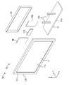
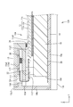
- FIG. 1 is an exploded perspective view showing a schematic configuration of a television receiver according to Embodiment 1 of the present invention.
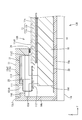
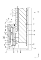
- Rear view of TV receiver Exploded perspective view showing a schematic configuration of a liquid crystal display unit constituting the liquid crystal display device Sectional drawing which shows the cross-sectional structure along the short side direction of a liquid crystal display device Sectional drawing which shows the cross-sectional structure along the long side direction of a liquid crystal display device Sectional drawing which shows the cross-sectional structure along the long side direction of the liquid crystal display device which concerns on Embodiment 2.
- FIG. Sectional drawing which shows the cross-sectional structure along the long side direction of the liquid crystal display device which concerns on Embodiment 3.
- FIG. 1 Sectional drawing which shows the cross-sectional structure along the long side direction of the liquid crystal display device which concerns on Embodiment 4.
- FIG. Sectional drawing which shows the cross-sectional structure along the short side direction of the liquid crystal display device which concerns on Embodiment 5.
- FIG. 1 is a diagrammatic drawing which shows the cross-sectional structure along the long side direction of the liquid crystal display device which concerns on Embodiment 4.
- Embodiment 1 of the present invention will be described with reference to FIGS. 1 to 5.
- a television receiver TV a liquid crystal display device 10, and a lighting device 12 are illustrated.
- Each drawing shows an X-axis, a Y-axis, and a Z-axis, and the directions of the axes are drawn in common directions in the drawings.
- the upper side shown in FIG. 4 is the front side (display surface side), and the lower side is the back side (back side).
- FIG. 1 is an exploded perspective view showing a schematic configuration of a television receiver TV according to Embodiment 1 of the present invention
- FIG. 2 is a rear view of the television receiver TV.
- the television receiver TV according to this embodiment includes a liquid crystal display unit LDU, various substrates PWB, MB, and CTB attached to the back side (back side) of the liquid crystal display unit LDU, and a liquid crystal display.
- a cover member CV attached to cover the various substrates PWB, MB, and CTB and a stand ST are provided on the back side of the unit LDU.
- the liquid crystal display unit LDU is supported by the stand ST so that the display surface 11c is along the vertical direction (Y-axis direction).
- the liquid crystal display device 10 is configured by removing at least a configuration for receiving a television signal (such as a tuner portion of the main board MB) from the television receiver TV having the above-described configuration.
- the liquid crystal display unit LDU has a horizontally long rectangular shape as a whole, and includes a liquid crystal panel 11 as a display panel and a backlight device (illumination device) 12 as an external light source, which are external appearances of the liquid crystal display device 10. It is the structure hold
- two stand mounting members STA extending along the Y-axis direction are spaced apart in the X-axis direction. A pair is attached.
- These stand attachment members STA have a substantially channel shape with a cross-sectional shape opened on the surface on the chassis 14 side, and a pair of support columns STb in the stand ST are inserted into a space formed between the stand 14 and the chassis 14. It is configured as follows.
- the wiring member (electric wire etc.) connected to the LED board 18 which the backlight apparatus 12 has passes through the space in the stand attachment member STA.
- the stand ST includes a pedestal portion STa that extends along the X-axis direction and the Z-axis direction, and a pair of support columns STb that rise from the pedestal portion STa along the Y-axis direction.
- the cover member CV is made of synthetic resin, and is attached so as to cover the lower half (see FIG. 2) on the back surface of the chassis 14 while traversing the pair of stand attachment members STA in the X-axis direction. Between the cover member CV and the chassis 14, a space capable of accommodating components such as various substrates PWB, MB, and CTB described later is formed.
- the various substrates PWB, MB, and CTB include a power supply substrate PWB, a main substrate MB, and a control substrate CTB.
- the power supply substrate PWB is a power supply source of the liquid crystal display device 10 and supplies driving power to the other substrates MB and CTB, the LEDs 17 included in the backlight device 12, and the like.
- the main board MB has a tuner section (not shown) that can receive a television signal and an image processing section (not shown) that performs image processing on the received television signal, and sends the processed image signal to the control board CTB. Output.
- the main board MB receives an image signal from the image reproduction device when the liquid crystal display device 10 is connected to an external image reproduction device (not shown).
- the processed signal is output to the control board CTB.
- the control board CTB has a function of converting an image signal input from the main board MB into a liquid crystal driving signal and supplying the converted liquid crystal driving signal to the liquid crystal panel 11.
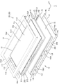
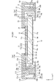
- FIG. 3 is an exploded perspective view showing a schematic configuration of the liquid crystal display unit LDU constituting the liquid crystal display device 10, and FIG. 4 is a cross-sectional view showing a cross-sectional configuration along the short side direction of the liquid crystal display device 10.
- FIG. 5 is a cross-sectional view showing a cross-sectional configuration along the long side direction of the liquid crystal display device 10.
- the liquid crystal display unit LDU constituting the liquid crystal display device 10 includes a frame (front frame) 13 whose main components are arranged on the front side and a chassis arranged on the back side. (Rear chassis) 14 is sandwiched between.
- the main components sandwiched between the frame 13 and the chassis 14 include at least the liquid crystal panel 11, the optical member 15, the light guide plate 16, the LED unit (light source unit) LU, and the reflection sheet 20. It is. Among these, the liquid crystal panel 11, the optical member 15, the light guide plate 16, and the reflection sheet 20 are held in a state where they are sandwiched between the front frame 13 and the back chassis 14 in a stacked state. .
- the backlight device 12 mainly includes an optical member 15, a light guide plate 16, an LED unit LU, a chassis 14, and a reflection sheet 20.
- the LED unit LU is arranged between the frame 13 and the chassis 14 so as to be along the end surface on the long side of the light guide plate 16.
- the LED unit LU includes an LED (LED light source) 17 that is a light source, an LED substrate (light source substrate) 18 on which the LED 17 is mounted, and a heat radiating member (light source support member) 19.
- the liquid crystal panel 11 has a horizontally long rectangular shape when seen in a plan view.
- the liquid crystal panel 11 has a configuration in which a pair of glass substrates 11a and 11b having excellent translucency are bonded together with a predetermined gap therebetween, and liquid crystal is sealed between the substrates 11a and 11b.
- the front side front side
- the back side rear side
- the array substrate 11b is the array substrate 11b.
- the TFT array substrate 11b is provided with a switching element (for example, a thin film transistor: TFT) connected to a source wiring and a gate wiring orthogonal to each other, a pixel electrode connected to the switching element, an alignment film, and the like. Yes.
- the array substrate 11b is provided with a large number of TFTs and pixel electrodes arranged side by side, and a large number of TFTs and pixel electrodes are arranged around the TFTs and pixel electrodes so as to surround a gate wiring and a source wiring in a lattice shape. It is installed.
- the gate wiring and the source wiring are connected to the gate electrode and the source electrode of the TFT, respectively, and the pixel electrode is connected to the drain electrode of the TFT.
- the array substrate 11b is provided with capacitor wirings (auxiliary capacitor wirings, storage capacitor wirings, Cs wirings) that are parallel to the gate wirings and overlap the pixel electrodes in plan view. Are arranged alternately in the Y-axis direction.
- the CF substrate 11a is provided with a color filter in which colored portions such as R (red), G (green), and B (blue) are arranged in a predetermined arrangement, a counter electrode, and an alignment film. .
- a polarizing plate (not shown) is disposed outside each of the substrates 11a and 11b.
- the array substrate 11b is formed to have a larger size in plan view than the CF substrate 11a, as shown in FIGS.
- the array substrate 11b is arranged in such a manner that its end protrudes outward from the end of the CF substrate 11a.
- the array substrate 11b is formed to be slightly larger than the CF substrate 11a so that its outer peripheral end protrudes outside the outer peripheral end of the CF substrate 11a over the entire periphery.
- the pair of long-side end portions constituting the outer peripheral end portion of the array substrate 11b the long-side end portion on the control substrate CTB side (front side shown in FIG. 3, left side shown in FIG.
- a flexible substrate (flexible wiring) 211 is connected to each source side terminal portion.
- a plurality of flexible substrates 211 are intermittently arranged in the X-axis direction, that is, in the direction along the long side end of the array substrate 11b. Each flexible substrate 211 protrudes outward along the Y-axis direction from the end on the long side of the array substrate 11b.
- a plurality of gate side terminal portions led from the gate wiring and the capacitor wiring are provided.
- a flexible substrate (flexible wiring) 111 is connected to each gate side terminal portion.
- a plurality of flexible substrates 111 are arranged intermittently in the Y-axis direction, that is, in the direction along the short side end of the array substrate 11b. Each flexible substrate 111 protrudes outward along the X-axis direction from the short-side end of the array substrate 11b.
- Each of the flexible substrates 111 and 211 includes a film-like base material made of a synthetic resin material having insulation properties and flexibility (for example, a polyimide resin), and a driver (panel drive) for driving a liquid crystal mounted on the base material. Parts) 112, 211.
- a large number of wiring patterns are formed on the base material of each flexible substrate 111, 211, and drivers 112, 212 mounted near the center of the base material are connected to the wiring pattern. ing.
- One end of the flexible substrate 211 is pressure-bonded to the source-side terminal portion of the array substrate 11b via an anisotropic conductive film (ACF), and the other end is a source-side print described later.
- ACF anisotropic conductive film
- a terminal (not shown) included in the substrate (source substrate) 213 is crimped and connected via an anisotropic conductive film (ACF).
- the printed board (source board) 213 is connected to the control board CTB described above via a wiring member (not shown).
- the printed circuit board 213 transmits a signal (a scanning signal to the gate wiring, a data signal to the source wiring, a capacitance signal to the capacity wiring, etc.) input from the control board CTB to the flexible substrate 211.
- the printed circuit board 213 has a long shape (band shape). In the case of this embodiment, two printed boards 213 are used, and these are connected to the respective flexible boards 211 so as to be aligned with each other.
- the length of one printed circuit board 213 is set to about half the long side of the liquid crystal panel 11.
- one end of the flexible substrate 111 is pressure-bonded to the gate side terminal portion of the array substrate 11b via an anisotropic conductive film (ACF), and the other end is described later.
- a terminal portion (not shown) of the printed circuit board (gate substrate) 113 on the gate side is crimped and connected via an anisotropic conductive film (ACF).
- the printed circuit board 113 has a long shape (band shape). In the case of this embodiment, the length of the printed circuit board 113 is set to the length of the short side of the liquid crystal panel 11.
- the array substrate 11b is formed with a relay wiring (not shown) connecting the source side terminal portion and the gate side terminal portion.
- Signals (scanning signal to the gate wiring, capacitance signal to the capacitance wiring, etc.) input from the control board CTB are transmitted to the gate side terminal portion, the flexible board 111, and the printed board 113 through the relay wiring.
- the liquid crystal panel 11 displays an image on the display surface 11c based on a signal input from the control board CTB.
- the liquid crystal panel 11 is placed on the front side (light emitting side) of the optical member 15 to be described later.
- the back surface of the liquid crystal panel 11 (the outer surface of the polarizing plate on the back side) is in close contact with the optical member 15 with almost no gap. This prevents dust and the like from entering between the liquid crystal panel 11 and the optical member 15.
- the display surface (front plate surface) 11c of the liquid crystal panel 11 is a display area 11c1 on the center side of the screen where an image can be displayed, and a frame shape (frame shape) which surrounds the display area on the outer peripheral edge side of the screen.
- each terminal part and each flexible substrate 111 and 211 described above are arranged in a non-display area.
- the optical member 15 has a horizontally long rectangular shape as viewed from above, like the liquid crystal panel 11.
- the size (short side dimension and long side dimension) of the optical member 15 is set to be equal to that of the liquid crystal panel 11.
- the optical member 15 is placed so as to be laminated on the front side (light emitting side) of the light guide plate 16 described later, and is disposed in a state of being sandwiched between the liquid crystal panel 11 and the light guide plate 16.
- Each of the optical members 15 is in the form of a sheet and is formed by stacking three pieces of each other.
- Specific examples of the optical member 15 include, for example, a diffusion sheet, a lens sheet, and a reflective polarizing sheet. Any of these can be used as appropriate.
- the light guide plate 16 is made of a synthetic resin material (for example, acrylic resin such as PMMA or polycarbonate) having a refractive index sufficiently higher than that of air and almost transparent (excellent translucency). As shown in FIG. 3, the light guide plate 16 has a horizontally long rectangular shape when seen in a plane, like the liquid crystal panel 11 and the optical member 15. The light guide plate 16 has a plate shape that is thicker than the optical member 15. The light guide plate 16 has a long side direction on the main surface that matches the X-axis direction, a short side direction that matches the Y-axis direction, and a plate thickness direction that is orthogonal to the main surface matches the Z-axis direction. It is drawn in each figure. As shown in FIGS.
- the light guide plate 16 is set to have a larger size (short side dimension and long side dimension) than the liquid crystal panel 11 when viewed from the front side.
- the end portion of the light guide plate 16 is disposed in the display device 12 so as to protrude outward from the end portion of the liquid crystal panel 11.
- the light guide plate 16 is formed to be slightly larger than the liquid crystal panel 11 so that its end protrudes outward from the outer peripheral end of the array substrate 11b of the liquid crystal panel 11 over the entire circumference.
- the light guide plate 16 is disposed on the back side of the optical member 15 and is sandwiched between the optical member 15 and the chassis 14.
- the LED units LU are arranged outside the two end portions on the long side of the light guide plate 16, and light from the LED units LU is introduced into the light guide plate 16 from the end portions.
- the light guide plate 16 has a function of rising and emitting light toward the optical member 15 side (front side) while propagating light from the LED unit LU introduced from the end portion on the long side.
- the front-side plate surface (the surface facing the optical member 15) 16 a emits light from the inside toward the optical member 15 and the liquid crystal panel 11 as shown in FIG. 4. It becomes the output surface 16a.
- both long-side end faces (both end faces possessed by both ends in the short-side direction) that are long along the X-axis direction are respectively.
- the LED 17 (LED substrate 18) faces the LED 17 at a predetermined interval, and these form a pair of light incident surfaces 16b on which light emitted from the LED 17 is incident.
- the light incident surface 16b is disposed in parallel along the X-axis direction and the Z-axis direction (the main plate surface of the LED substrate 18), and is substantially orthogonal to the light emitting surface 16a.
- a reflection sheet 20 for reflecting the light in the light guide plate 16 toward the light emitting surface 16 side is disposed.
- the reflection sheet 20 is provided so as to cover the entire plate surface 16 c on the back side of the light guide plate 16.
- the reflection sheet 20 is disposed in the display device 12 so as to be sandwiched between the chassis 14 and the light guide plate 16.
- the reflection sheet 20 is made of a synthetic resin sheet (for example, a foamed polyethylene terephthalate sheet) having a white surface with excellent light reflectivity.
- the reflective sheet 20 has at least a short side dimension set larger than the short side dimension of the light guide plate 16, and both ends thereof are closer to the LED 17 than the light incident surface 16 b of the light guide plate 16. It is arranged in a state of protruding.
- At least one of the light exit surface 16a and the back plate surface 16c of the light guide plate 16 is a reflecting portion (not shown) that reflects the light inside the light guide plate 16, or the light inside the light guide plate 16 is scattered.
- the scattering portion (not shown) is patterned so as to have a predetermined in-plane distribution. Accordingly, the light emitted from the light emitting surface 16a is controlled to have a uniform distribution in the surface.
- the LED 17 constituting the LED unit LU has a configuration in which an LED chip is sealed with a resin material on a substrate portion fixed to the LED substrate 18.
- the LED chip mounted on the substrate unit has a single main emission wavelength. Specifically, the LED chip that emits blue light in a single color is used.
- a phosphor that emits a predetermined color when excited by blue light emitted from the LED chip is dispersed and blended.
- the resin material is generally configured to emit white light.
- the phosphor for example, a suitable combination of a yellow phosphor that emits yellow light, a green phosphor that emits green light, and a red phosphor that emits red light may be used. They may be used alone.
- the LED 17 is a so-called top emission type in which a surface opposite to the mounting surface with respect to the LED substrate 18 (a plate surface facing the light incident surface 16b of the light guide plate 16) is the main light emitting surface 17a.
- the LED substrate 18 is an elongated plate shape (strip shape, long shape) extending along the long side direction of the light guide plate 16 (X-axis direction, longitudinal direction of the light incident surface 16 b). Shape).
- the LED substrate 18 has a posture in which the main surface is along the X-axis direction and the Z-axis direction (that is, a posture aligned in parallel with the light incident surface 16b of the light guide plate 16). It is accommodated in the frame 13 and the chassis 14.
- the length (dimension) of the LED substrate 18 in the longitudinal direction is set to about half of the long side of the light guide plate 16.
- the LED 17 is surface-mounted on a plate surface (mounting surface) 18 a facing the light guide plate 16 side of the LED substrate 18.
- a plurality of LEDs 17 are arranged in a line on the mounting surface 18a of the LED substrate 18 along the length direction (X-axis direction) at a predetermined interval. Further, the columns of LEDs 17 are arranged in parallel along the long side direction of the light guide plate 16. The distance between the LEDs 17 adjacent in the X-axis direction (that is, the arrangement pitch of the LEDs 17) is set to be approximately equal. Note that the arrangement direction of the LEDs 17 coincides with the length direction (X-axis direction) of the LED substrate 18.
- a metal film for example, copper foil that extends along the longitudinal direction (X-axis direction) of the LED substrate 18 and connects adjacent LEDs 17 across the LEDs 17 in series on the mounting surface 18 a of the LED substrate 18.
- a wiring pattern (not shown) is formed. The terminal portions formed at both ends of the wiring pattern are connected to the power supply substrate PWB via wiring members such as connectors and electric wires, so that driving power is supplied to each LED 17.
- the LED boards 18 that are paired with the light guide plate 16 in between are housed in the frame 13 and the chassis 14 with the mounting surfaces 18a of the LEDs 17 facing each other, and are thus mounted on the paired LED boards 18 respectively.
- the main light emitting surfaces 17a of the LEDs 17 are opposed to each other, and the optical axes of the LEDs 17 substantially coincide with the Y-axis direction.
- the base material of the LED substrate 18 is made of a metal such as aluminum, for example, and the wiring pattern (not shown) described above is formed on the surface thereof via an insulating layer.
- insulating materials such as a ceramic, can also be used.
- the heat dissipation member 19 is made of a metal having excellent thermal conductivity such as aluminum.
- the heat dissipating member 19 includes an LED attachment portion (light source attachment portion) 19a to which the LED substrate 18 is attached, and a heat dissipating portion 19b in surface contact with the plate surface of the chassis 14, and these are bent with an approximately L-shaped cross section. It has a shape.
- the heat radiation member 19 has a length dimension set to be approximately the same as the length dimension of the LED substrate 18 described above.
- the LED mounting portion 19 a has a plate shape that is arranged in parallel with the plate surface 18 a of the LED substrate 18 and the light incident surface 16 b of the light guide plate 16.
- the long side direction of the LED attachment portion 19a coincides with the X-axis direction
- the short side direction coincides with the Z-axis direction
- the thickness direction coincides with the Y-axis direction.
- the LED board 18 is attached to the inner plate surface (that is, the plate surface facing the light guide plate 16 side) of the LED mounting portion 19a.
- the LED mounting portion 19 a has a long side dimension substantially equal to the long side dimension of the LED substrate 18, but the short side dimension is set to be larger than the short side dimension of the LED substrate 18. And the both ends of the short side direction in the LED attachment part 19a protrude outward from the both ends of the LED board 18 along the Z-axis direction.
- the outer plate surface (that is, the plate surface opposite to the plate surface on which the LED substrate 18 is mounted) of the LED mounting portion 19a faces a screw mounting portion 21 included in the frame 13 described later. That is, the LED attachment portion 19 a is disposed in the display device 12 so as to be interposed between the screw attachment portion 21 of the frame 13 and the light guide plate 16.
- the LED mounting portion 19a extends along the Z-axis direction (the overlapping direction of the liquid crystal panel 11, the optical member 15, and the light guide plate 16) from the inner end of the heat radiating portion 19b (that is, the end on the LED 17 (light guide plate 16) side). It stands up toward the front side (that is, the frame 13 side).
- the heat radiating portion 19 b has a plate shape arranged in parallel to the plate surface of the chassis 14.
- the long side direction of the heat dissipating part 19b coincides with the X-axis direction
- the short side direction coincides with the Y-axis direction
- the thickness direction coincides with the Z-axis direction.
- the heat dissipating part 19b protrudes from the back end (that is, the end on the chassis 14 side) of the LED mounting part 19a toward the outside (that is, the side opposite to the light guide plate 16 side) along the Y-axis direction.
- the long side dimension of the heat dissipating part 19b is set to be substantially the same as that of the LED attaching part 19a.
- the entire plate surface on the back side of the heat radiating portion 19b (that is, the plate surface facing the chassis 14) is in surface contact with the plate surface of the chassis 14.
- plate surface on the opposite side to the contact surface with respect to the chassis 14) of the heat radiation part 19b opposes the screw attachment part 21 which the flame
- the heat generated with the lighting of the LED 17 is transmitted to the frame 13 having the chassis 14 and the screw mounting portion 21 via the LED substrate 18, the LED mounting portion 19 a and the heat radiating portion 19 b.
- the heat radiating portion 19b is provided with an insertion hole 19b1 through which the screw member SM is passed. The heat radiating portion 19b is fixed to the screw mounting portion 21 of the frame 13 by using the screw member SM.
- the frame 13 and the chassis 14 are both made of metal such as aluminum, and have high mechanical strength (rigidity) and thermal conductivity.
- the frame 13 and the chassis 14 hold the LED unit LU, and hold a laminate composed of the liquid crystal panel 11, the optical member 15, the light guide plate 16, and the reflection sheet 20 so as to be sandwiched between the front side and the back side.
- the frame 13 has a frame shape surrounding the display area 11c1 on the display surface 11c of the liquid crystal panel 11, and has a horizontally long rectangular shape as a whole.
- the frame 13 mainly includes a frame-like frame-shaped main body portion 13a disposed on the front side of the liquid crystal panel 11, and a side wall portion 13b extending from the outer edge portion of the frame-shaped main body portion 13a toward the back side.
- the frame-shaped main body 13a is divided into a long-side frame-shaped main body 13a1 and a short-side frame-shaped main body 13a2.
- the side wall part 13b is mainly provided in the outer edge part of the frame-like main-body part 13a1 of a long side.
- the side wall part 13b has a shape extending perpendicularly to the frame-shaped main body part 13a.
- the frame-shaped main body 13a is arranged on the front side of the liquid crystal panel 11 so as to cover the non-display area 11c2 on the display surface 11c.
- a screw mounting portion 21 on the back side of the long side frame-like main body 13 a 1, there are a screw mounting portion 21, a light guide plate pressing portion 23, and a protrusion 24 for pressing the liquid crystal panel 11. 4 is provided so as to protrude toward the lower side (chassis 14 side).
- the screw attachment portion 21 is provided on the side wall portion 13b side most, and the protrusion 24 is provided on the innermost edge side.
- the screw attachment part 21 becomes the shape which protruded to the back side (chassis 14 side) longest among these, and the protrusion 24 became the shape which protruded to the back side (chassis 14 side) shortest.
- the screw attachment portion 21 has an elongated shape along the long side direction of the frame 13 (frame-shaped main body portion 13a), and a groove portion 21a into which the screw member SM can be screwed is formed at the tip. .
- the light guide plate pressing portion 23 provided in the long side frame-like main body portion 13a1 is a portion that presses the end portion on the long side of the light guide plate 16 from the front side toward the chassis 14 side.
- the light guide plate pressing portion 23 also has an elongated shape along the long side direction of the frame 13 (frame-shaped main body portion 13a), like the screw mounting portion 21.
- the light guide plate pressing portion 23 is partially provided with a notch portion 23 a penetrating along the short side direction (Y-axis direction) of the frame 13.
- a source-side flexible substrate 211 provided at the end of the liquid crystal panel 11 is passed through the notch 23a.
- the source-side printed circuit board 213 is in an upright state with respect to the chassis 14 as shown in FIG. That is, the printed circuit board 213 is arranged between the frame 13 and the chassis 14 in a state where the short side direction is along the thickness direction (Z-axis direction) of the light guide plate 16.
- the protruding portion 24 also has a shape extending elongated along the long side direction of the frame 13 (frame-shaped main body portion 13 a).
- the protrusion 24 is made of an elastic body having a light shielding property (for example, a black rubber elastic body).
- the protrusion 24 is set so as to hold the non-display area 11c2 of the liquid crystal panel 11. As shown in FIG. 4, there is a gap between the protruding portion 24 and the light guide plate pressing portion 23, and the end of the liquid crystal panel 11 connected to the flexible substrate 211 is disposed in this gap.
- a light guide plate pressing portion 23 and a projecting portion 24 are respectively provided on the lower side (chassis 14 side). ) Is provided in a protruding shape.
- the light guide plate pressing portion 23 provided in the short-side frame-shaped main body portion 13a2 is a portion that presses the end portion on the short side of the light guide plate 16 from the front side toward the chassis 14 side.
- the light guide plate pressing portion 23 has an elongated shape along the short side direction of the frame 13 (frame-shaped main body portion 13a).
- maintenance part 23 provided in the frame-like main-body part 13a2 of a short side is connected to the edge part of the light-guide plate holding
- the light guide plate pressing portion 23 has a frame shape surrounding the display area 11 c 1 of the liquid crystal panel 11 as a whole.
- the light guide plate holder 23 provided in the frame-like main body 13a1 on the short side is also partially provided with a notch 23a penetrating along the long side direction (X-axis direction) of the frame 13. ing.
- the flexible substrate 111 on the gate side is passed through the notch 23a.
- the projection 24 provided on the short-side frame-shaped main body 13a2 presses the end (non-display area 11c2) on the short side of the liquid crystal panel 11 from the front side toward the chassis 14 (light guide plate 16). It has become a part.
- the protrusion 24 has an elongated shape along the short side direction of the frame 13 (frame-shaped main body 13a).
- the edge part of the projection part 24 provided in the frame-like main-body part 13a2 of the short side is connected to the edge part of the projection part 24 provided in the frame-like main body part 13a1 of the long side. That is, the protrusion 24 has a frame shape surrounding the display area 11 c 1 of the liquid crystal panel 11 as a whole.
- the projection 24 on the short side is also made of the same elastic body as that on the long side.
- the short-side frame-like main body 13 a 2 has a plate shape having a predetermined thickness that spreads along the plate surface of the chassis 14 (the plate surface of the liquid crystal panel 11). There is no.
- a groove-shaped accommodation portion 13c extending along the short side direction of the frame 13 is provided inside the frame-shaped main body portion 13a2.
- the accommodating portion 13c is a space for accommodating a printed circuit board (an example of a gate substrate or a driving substrate) 113 on the gate side.
- the accommodating portion 13c has a shape that is recessed from the outer edge of the frame-like main body portion 13a2 on the short side toward the inner edge.
- the flexible board 111 connected to the printed board 113 is passed through the hole 13d.
- the printed circuit board 113 on the gate side is accommodated in the accommodating portion 13c so as to be inserted from the outer edge side to the inner edge side of the frame-shaped main body portion 13a2.
- the flexible substrate 111 connected to the end portion of the printed circuit board 113 is folded back toward the inner side of the liquid crystal panel 11 (display area 11c1 side). A part of the flexible substrate 111 folded in this way is in a state of penetrating through the hole 13d in the thickness direction (Z-axis direction) of the frame-shaped main body 13a.
- the printed circuit board 113 is accommodated in a state in which the plate surface is kept slightly spaced from the wall surface (inner wall) of the accommodating part 13c.
- the printed circuit board 113 is arranged substantially parallel to the liquid crystal panel 11 so as to face the non-display area 11c2 of the liquid crystal panel 11 in the housing portion 13c.
- the side wall part 13b is provided in the outer edge part of the frame-shaped main-body part 13a1 by the side of a long side.
- the side wall portion 13b is arranged so as to cover the end surface on the long side of the laminate composed of the liquid crystal panel 11, the optical member 15, the light guide plate 16, and the reflection sheet 20.
- the inside of the distal end portion of the side wall portion 13 b is in close contact with the end portion of the chassis 14.
- the chassis 14 is generally composed of a horizontally long plate-like member like the liquid crystal panel 11 and the like, and covers the plate surface 16c on the back side of the light guide plate 16 so as to cover the liquid crystal display unit LDU (liquid crystal display). Arranged on the back side of the device 10).
- the chassis 14 includes a rectangular plate-shaped chassis main body portion 14a, a light source housing portion 14b extending from an end portion on the long side of the chassis main body portion 14a, and an end on the short side of the chassis main body portion 14a. And an upright wall portion 14c erected on the portion.
- the chassis main body portion 14 a is a portion addressed to the plate surface 16 c on the back side of the light guide plate 16 through the reflection sheet 20, and occupies most of the chassis 14.
- the chassis main body 14 a is in close contact with the plate surface 16 c on the back side of the light guide plate 16 via the reflection sheet 20.
- the light source accommodating portion 14b has a shape that rises toward the back side of the chassis main body portion 14a, and as a whole, has a shallow container shape extending along the long side direction. As shown in FIG. 4, the LED unit LU that is fixed to the screw attachment portion 21 of the frame 13 is accommodated in the groove-like space inside the light source accommodation portion 14 b.
- the standing wall portion 14c has a plate shape rising from the end portion on the short side of the chassis main body portion 14a along the thickness direction (Z-axis direction) of the light guide plate 16 and the like.
- the standing wall portion 14c is provided at each of the two short-side ends of the chassis main body portion 14a.
- line part is set so that it may fit with the inlet 13c1 of the accommodating part 13c with which the frame-like main-body part 13a2 of the short side in the flame
- the standing wall portion 14c constitutes an end surface portion surrounding the liquid crystal display unit LDU (liquid crystal display device 10) together with the side wall portion 13b included in the frame 13.
- LDU liquid crystal display device
- the end portion on the long side of the chassis 14 (that is, the light source accommodating portion 14b) is provided with two types of insertion holes 25A and 25B.
- One large insertion hole 25A is for exposing an end (head) of the screw member SM used when the heat radiating member 19 is fixed to the screw mounting portion 21. Larger than the head).
- the other small insertion hole 25B is a hole through which the screw member SM used to fix the chassis 14 to the frame 13 is inserted.
- the screw member SM is inserted into the insertion hole 25B, and the screw member SM is further inserted into a predetermined insertion hole 19b1 provided in the heat dissipation member 19 (heat dissipation portion 19b).
- the screw member SM is fixed to the frame 13 by being screwed while being inserted into the groove 21a.
- the chassis 14 By fixing the chassis 14 to the frame 13 in this way, a laminate composed of the liquid crystal panel 11, the optical member 15, the light guide plate 16, and the reflection sheet 20 and the LED unit LU arranged on the periphery thereof are combined with the frame. 13 and the chassis 14 are held.
- the frame 13 is installed on a predetermined work table.
- the frame 13 on the workbench is in a state where the front side faces the lower side (workbench side) and the back side faces the upper side.
- the liquid crystal panel 11 is assembled on the upper side of the frame 13 on the work table (that is, the back side of the frame 13).
- the liquid crystal panel 11 is in a state in which the CF substrate 11a is disposed on the lower side (workbench side) and the array substrate 11b is disposed on the upper side.
- the printed circuit board 113 on the gate side provided in the liquid crystal panel 11 is inserted into the accommodating portion 13 c provided in the frame-shaped main body portion 13 a of the frame 13.
- the optical member 15 is placed on the back side (the array substrate 11 b side) of the liquid crystal panel 11.
- the LED unit LU is placed on the screw mounting portion 21 with the LED mounting portion 19a of the heat radiating member 19 disposed on the lower side and the heat radiating portion 19b disposed on the upper side.
- the LED unit LU is fixed on the screw mounting portion 21 of the frame 13 using the screw member SM.
- the light guide plate 16 is placed on the optical member 15.
- the light guide plate 16 is in a state where the front-side plate surface 16a serving as the light emitting surface 16a is arranged on the lower side and the back-side plate surface 16c is arranged on the upper side.
- the light guide plate 16 is placed on the frame 13 such that the peripheral portion of the front plate surface 16 a is in contact with the light guide plate pressing portion 23 of the frame 13.
- the light guide plate 16 is positioned with respect to the frame 13 so that the interval (distance) between the end surface (light incident surface) 16b and the LED unit LU is a predetermined interval.
- the reflection sheet 20 is assembled on the plate surface 16 c on the back side of the light guide plate 16.
- the chassis 14 is assembled to the frame 13 in a state where the chassis 14 is placed on the plate surface 16 c of the light guide plate 16 via the reflection sheet 20.
- the chassis 14 is fixed to the screw mounting portion 21 of the frame 13 using the screw member SM.
- the protruding line part 14d with which the standing wall part 14c of the chassis 14 is equipped is fitted by the inlet 13c1 of the accommodating part 13c with which the frame-like main-body part 13a2 of the short side of the flame
- frame 13 is equipped.
- Each component of the liquid crystal display unit LDU is assembled by the above operation procedure.
- the liquid crystal display unit LDU is assembled with the stand mounting member STA and the various substrates PWB, MB, and CTB on the back side thereof, and further the stand ST and the cover member CV are assembled, whereby the liquid crystal display device of the present embodiment. 10 and the television receiver TV are manufactured.
- each LED 17 constituting the circuit is driven.
- each LED 17 is driven and light is emitted from each LED 17, light is incident on the inside from the light incident surface 16 c of the light guide plate 16.
- the incident light is reflected by the reflection sheet 20 laid on the back side of the light guide plate 16 and proceeds in the light guide plate 16, and from the front side plate surface (light emitting surface) 16 a toward the optical member 15. Emitted.
- the emitted light passes through the optical member 15 and becomes light that spreads substantially uniformly in a planar shape, and illuminates the back surface of the liquid crystal panel 11.
- the liquid crystal panel 11 displays an image on the display surface 11c (display area 11c1) by using the light spread in a planar shape.
- the printed circuit board 113 on the gate side as a driving substrate is accommodated in the accommodating portion 13c included in the frame 13.
- the printed circuit board 113 is arranged on the front side of the liquid crystal panel 11 so as to be arranged in parallel to the liquid crystal panel 11, so that at least a portion where the printed circuit board 113 on the gate side is disposed is arranged in the liquid crystal display device 10.
- the width in the short direction (hereinafter referred to as the short width) of the long printed board 113 is generally set larger than the thickness of the light guide plate 16. Therefore, it can be said that the liquid crystal display device 10 of this embodiment is thinner than the case where the short side direction of the printed circuit board 113 is arranged along the thickness direction of the light guide plate 16 (liquid crystal panel 11).
- the liquid crystal display device 10 of the present embodiment is accommodated in the accommodating portion 13c of the frame 13 so that the printed board 113 is disposed on the front side of the liquid crystal panel 11 in a state of facing the non-display area 11c2, the display area The non-display portion (frame portion) surrounding 11c1 can be set narrow (small).
- the source side printed circuit board 213 is accommodated in the liquid crystal display device 10 in a state where the short side direction is along the thickness direction of the light guide plate 16. In this manner, only the printed circuit board 113 on the gate side is accommodated in the accommodating portion 13 c provided on the frame 13, and the printed circuit board 213 on the source side is disposed between the frame 13 and the chassis 14 in a state along the thickness direction of the light guide plate 16. May be accommodated.
- the accommodating portion 13c provided in the frame-shaped main body portion 13a of the frame 13 has a shape that is recessed from the outer edge of the frame-shaped main body portion 13a toward the inner edge. . Therefore, the printed board 113 as a drive board can be accommodated in the accommodating portion 13c in a form of being inserted from the outer edge toward the inner edge. Therefore, the liquid crystal display device 10 of the present embodiment has a structure in which the printed board 113 can be easily attached to the housing portion 13 c and the printed board 113 can be easily fixed to the frame 13.
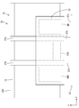
- FIG. 6 is a cross-sectional view illustrating a cross-sectional configuration along the long side direction of the liquid crystal display device 10A according to the second embodiment.
- the portion of the liquid crystal display device 10A of the present embodiment shown in FIG. 6 corresponds to the portion of the liquid crystal display device 10 of the first embodiment shown in FIG.
- the basic configuration of the liquid crystal display device 10A (illumination device 12A) of the present embodiment is the same as that of the first embodiment.
- the spacer portion 30 is accommodated in the accommodating portion 13c of the frame 13 together with the printed circuit board 113 on the gate side.
- the spacer 30 is made of an insulating elastic body (for example, urethane foam) having a rectangular parallelepiped shape.
- the spacer portion 30 is interposed between the printed board 113 and the lower wall surface (back side of the frame-shaped main body portion 13 a 2) of the housing portion 13 c.
- the printed circuit board 113 is brought into close contact with the upper wall surface (the front side of the frame-shaped main body portion 13a2) of the housing portion 13c.
- the spacer portion 30 is not directly fixed to the printed circuit board 113 and is a separate component from the printed circuit board 113.
- a plurality of spacer portions 30 are used, and each spacer portion 30 is arranged along the longitudinal direction of the printed circuit board 113 in the accommodating portion 13c with a predetermined distance from each other.
- the spacer portion 30 is slightly elastically deformed when housed in the housing portion 13c together with the printed circuit board 113, and is positioned in a state in which the printed circuit board 113 is pressed against the wall surface of the housing portion 13c.
- the spacer portion 30 may be composed of one elongated member.
- the printed circuit board 113 may be positioned in the accommodating portion 13c using the spacer portion 30.
- the printed circuit board 113 is thus positioned, unnecessary movement of the printed circuit board 113 in the accommodating portion 13c is suppressed. That is, when the liquid crystal display device 10A receives vibration or the like, the printed circuit board 113 moves in the housing portion 13c, and the collision between the printed circuit board 113 and the wall surface of the housing portion 13c is avoided, and the collision sound is Generation etc. are suppressed.
- the printed circuit board 113 is brought into close contact with the frame 13 using the spacer unit 30. That is, the heat generated from the printed circuit board 113 and the like is easily moved efficiently to the frame 13 made of metal and excellent in heat dissipation. Therefore, the liquid crystal display device 10A has a structure excellent in cooling performance (heat dissipation performance).
- FIG. 7 is a cross-sectional view illustrating a cross-sectional configuration along the long side direction of the liquid crystal display device 10B according to the third embodiment.
- the portion of the liquid crystal display device 10B of the present embodiment shown in FIG. 7 corresponds to the portion of the liquid crystal display device 10 of the first embodiment shown in FIG.
- the basic configuration of the liquid crystal display device 10B (illumination device 12B) of the present embodiment is the same as that of the first embodiment.
- the shape of the accommodating portion 13cB provided in the frame 13 is different from that of the first embodiment.
- the frame-shaped main body portion 13a2 included in the frame 13 is not recessed from the outer edge toward the inner edge as in the first embodiment, but the back side of the frame-shaped main body portion 13a2 is generally depressed toward the front side. It has a shape like this. That is, the housing part 13cB of the present embodiment has a shape in which the wall on the back side of the housing part 13c of the first embodiment is removed. Therefore, the hole 13e through which the flexible board 111 connected to the printed board 113 passes is larger than that of the first embodiment. In addition, about the inner edge part of the flame
- the printed circuit board 113 is attached to the frame-like main body 13a2 of the frame 13 (the wall surface of the accommodating portion 13cB) via a layered adhesive material 31.
- the housing portion 13cB provided in the frame 13 does not need to have a groove shape that is recessed from the outer edge toward the inner edge as in the first embodiment, and at least the printed circuit board 113 is liquid crystal. What is necessary is just to be able to be accommodated so as to face the non-display area 11c2 of the panel 11. Further, as in the liquid crystal display device 10 ⁇ / b> B of the present embodiment, the printed circuit board 113 may be attached to the frame 13 using a predetermined adhesive material 31.
- FIG. 8 is a cross-sectional view illustrating a cross-sectional configuration along the long side direction of the liquid crystal display device 10C according to the fourth embodiment.
- the portion of the liquid crystal display device 10C of the present embodiment shown in FIG. 8 corresponds to the portion of the liquid crystal display device 10 of the first embodiment shown in FIG.
- the basic configuration of the liquid crystal display device 10C (illumination device 12C) of the present embodiment is the same as that of the second embodiment. That is, the liquid crystal display device 10C of the present embodiment includes the spacer portion 30C as in the second embodiment.
- the spacer portion 30C used in the present embodiment is different from that in the second embodiment in that the spacer portion 30C is made of thermally conductive silicone rubber.
- the thermally conductive silicone rubber used for the spacer portion 30C is made of a silicone rubber in which metal powder (filler) is dispersed and blended, and is excellent in thermal conductivity.
- the spacer part 30C the heat generated from the printed circuit board 113 and the like can be efficiently transferred to the frame 13 via the spacer part 30C. Therefore, the liquid crystal display device 12C of this embodiment further has a structure with excellent heat dissipation.
- the spacer portion 30C is fixed on the plate surface of the printed circuit board 113 using an adhesive. Therefore, the spacer part 30C is easily accommodated in the accommodating part 13c.
- FIG. 9 is a cross-sectional view illustrating a cross-sectional configuration along the short side direction of the liquid crystal display device 10D according to the fifth embodiment.
- the portion of the liquid crystal display device 10D of the present embodiment shown in FIG. 9 corresponds to a part of the liquid crystal display device 10 of the first embodiment shown in FIG.
- the chassis 14D has the standing wall portions 14c erected from the four sides of the rectangular chassis main body portion 14a. Has been. That is, the chassis 14D has a shallow box shape as a whole.
- the structure of the frame 13D is also different from that of the first embodiment, and the frame 13D does not have the side wall portion 13b as in the first embodiment, and only the frame-shaped main body portion 13Da having a frame shape as a whole. Consists of.
- the frame 13D is provided with a housing portion 13Dc for housing a source side printed board (an example of a drive board) 213 provided in the liquid crystal panel 11 of the present embodiment.
- the inlet 13Dc1 of the accommodating portion 13Dc is fitted with a protruding portion 14d of the standing wall portion 14c that is erected at the end portion on the long side of the chassis main body portion 14a.
- a hole 13Dd through which the flexible board 211 connected to the printed board 213 passes is provided in the frame-like main body 13Da1 on the long side.
- the configuration on the short side of the liquid crystal display device 10D (that is, the configuration that accommodates the printed circuit board 113 on the gate side) is the same as that in the first embodiment.
- the source-side printed board 213 may be housed in the housing portion 13Dc provided in the frame 13 in the same manner as the gate-side printed board 113 (see Embodiment 1). Similarly to the gate side, this printed circuit board 213 is accommodated in the accommodating portion 13Dc, so that it faces the non-display area 11c2 of the liquid crystal panel 11 and is arranged in parallel with the liquid crystal panel 11 so as to face the non-display area 11c2. It is arranged in.
- the liquid crystal display device 10D of the present embodiment is not only thin on the gate side (the short side of the liquid crystal display device 10D) but also on the source side (the long side of the liquid crystal display device 10D).
- the portion can be narrowed.
- the liquid crystal display device 10D of the present embodiment has a structure that is particularly advantageous for thinning.
- the LED substrate 18 on which the LEDs 17 are mounted is attached to the inside of the standing wall portion 14c of the chassis 14D.
- the gate-side printed board 113 is accommodated in the accommodating portion 13c of the frame 13, but in other embodiments, for example, the source-side printed board 213 is The structure accommodated in the groove-shaped accommodating part provided in the flame
- frame 13 may be sufficient.
- the frame 13 is appropriately provided with holes through which wirings connected to the printed circuit board 213 pass.
- the printed circuit board 113 is housed in the form of being inserted into the housing portion 13c of the frame 13.
- the printed board 113 may be attached to the wall surface of the housing portion 13c via an adhesive material and positioned in the housing portion 13c, or a fixing member such as a screw may be used.
- the printed circuit board 113 may be fixed and positioned on the wall surface (the frame-shaped main body portion 13a) of the housing portion 13c.
- the printed circuit board 113 has a long shape (a rectangular shape that is elongated).
- the shape of the gate substrate is not limited to this, and other shapes are used. May be.
- the printed circuit board 113 is arranged on the front side of the liquid crystal panel 11 so as to partially overlap (oppose) the non-display area 11c2 of the liquid crystal panel 11.
- the printed circuit board 113 is not displayed as long as the liquid crystal display device 10 can be thinned and the frame portion (a portion of the liquid crystal display device 10 surrounding the display region 11c1) can be narrowed. It does not have to be opposed to the region 11c2.
- the printed circuit board 113 is accommodated in the accommodating portion 13c of the frame 13 so as to be arranged in parallel to the plate surface (display surface 11c) of the liquid crystal panel 11. From the viewpoint of reducing the thickness of the liquid crystal display device 10, it is preferable to arrange the printed circuit board 113 in parallel with the plate surface of the liquid crystal panel 11 as described above. However, in other embodiments, the printed circuit board 113 may be housed in the housing portion 13c of the frame 13 with the plate surface of the printed circuit board 113 inclined.
- the spacer portion 30 is not directly fixed to the printed circuit board 113. Therefore, after inserting the printed circuit board 113 in the accommodating part 13c, the spacer part 30 was inserted in the clearance gap between the printed circuit board 113 and the wall surface of the accommodating part 13c.
- the spacer portion 30 may be fixed in advance to a predetermined portion of the printed circuit board 113 using an adhesive or the like. If the spacer part 30 is fixed on the printed circuit board 113 in this way, when the printed circuit board 113 is inserted into the accommodating part 13c of the frame 13, the spacer part 30 is also accommodated in the accommodating part 13c together. become. That is, when the spacer part 30 is fixed in advance at a predetermined position on the plate surface of the printed circuit board 113, the spacer part 30 is easily accommodated in the accommodating part 13c.
- the spacer portion 30 is made of an elastic body. That is, the spacer portion 30 is elastically deformed when sandwiched between the printed board 113 and the wall surface of the accommodating portion 13c.
- the spacer portion 30 is made of an elastic body as described above, the printed circuit board 113 is accommodated in close contact with the wall surface of the accommodating portion 13c, so that the printed circuit board 113 is positioned in the accommodating portion 13c and the printed circuit board 113 is also positioned. The heat generated from the printed circuit board 113 easily moves from the printed circuit board 113 to the frame 13.
- a member that is not elastically deformed may be selected as the spacer portion, and the spacer portion may be used to fill a gap formed between the printed board 113 and the wall surface of the accommodating portion 13c.
- the television receiver TV is exemplified as the display device.
- the liquid crystal display device may be used for, for example, a mobile phone or a portable information terminal.
- a display device that does not include a tuner unit may be used.
- the color filter of the color filter included in the liquid crystal panel 11 is exemplified as having three colors of R, G, and B. In other embodiments, the color section is set to four or more colors. Also good. In another embodiment, a liquid crystal display device that performs monochrome display may be used.
- TFT is used as the switching element of the liquid crystal display device in the first embodiment
- a switching element other than the TFT for example, a thin film diode (TFD)
- TFT thin film diode
- the LED 17 is used as the light source.
- other light sources such as a cold cathode tube may be used.
- SYMBOLS 10 Liquid crystal display device (display device), 11 ... Liquid crystal panel (display panel), 12 ... Illuminating device (backlight device), 13 ... Frame, 13a ... Frame-shaped main-body part, 13a1 ... Frame-like main-body part of a long side 13a2 ... Short-side frame-shaped main body part, 13b ... Side wall part, 13c ... Accommodating part, 14 ... Chassis, 14a ... Chassis main body part, 14b ... Light source accommodating part, 14c ... Standing wall part, 14d ... Round ridge part DESCRIPTION OF SYMBOLS ... Optical member, 16 ... Light guide plate, 16a ...
Landscapes
- Physics & Mathematics (AREA)
- Nonlinear Science (AREA)
- Mathematical Physics (AREA)
- Chemical & Material Sciences (AREA)
- Crystallography & Structural Chemistry (AREA)
- General Physics & Mathematics (AREA)
- Optics & Photonics (AREA)
- Liquid Crystal (AREA)
Abstract
表示装置(10)は、画像が表示される表示領域(11c1)と、表示領域(11c1)を囲む枠状の非表示領域(11c2)とをそれぞれ表側に有する表示パネル(11)と、表示パネル(11)の表示駆動を制御する駆動基板(113)と、表示パネル(11)と駆動基板(113)との間を電気的に接続すると共に、駆動基板(113)が表示パネル(11)の表側に配されるように折り返されるフレキシブル配線(111)と、非表示領域(11c2)を覆うように表示パネル(11)の表側に配される枠状本体部(13a)と、この枠状本体部(13a)の内部に設けられると共に駆動基板(113)を収容する収容部(13c)とを有するフレーム(13)と、を備える。
Description
本発明は、表示装置、及びテレビ受信装置に関する。
テレビ、携帯電話、携帯情報端末の表示装置に、液晶パネルが利用されている。液晶パネルは、液晶層と、この液晶層を挟んで互いに対向する一対のガラス基板とを備えている。これらのガラス基板には、それぞれ所定の電極が形成されており、これらの電極間に駆動電圧が印加されることによって、液晶層中の液晶分子の配向が制御される。
液晶パネルは、画像を表示させるために外部の光を利用する必要がある。そのため、この種の表示装置は、液晶パネルと共に、液晶パネルに光を供給するための照明装置(所謂、バックライト装置)を備えている。この照明装置は、液晶パネルの背面側に配されており、面状に広がった光を液晶パネルの背面に向けて照射するように構成されている。上述したように、液晶層中の液晶分子の配向が制御されると、液晶パネルをその背面側から表示面側に向かって透過する光の割合が調節されて、液晶パネルの表示画に画像が表示される。
なお、特許文献1に示されるように、液晶パネルの端部には、フレキシブル配線を介して駆動基板(ソース基板、ゲート基板)が設けられており、これらの駆動基板によって、前記駆動電圧が制御されている。
また、特許文献1に示されるように、前記駆動基板は、液晶パネルの端部から背面側に向かって延びた状態(つまり、駆動基板が液晶パネルの板面に対して垂直な状態)で、表示装置内に設置されている。なお、前記駆動基板は、全体的には、長尺状をなしており、その長手方向が液晶パネルの端部に沿って配されている。また、前記駆動基板の短手方向が、液晶パネルの板面に対して垂直に配されている。前記駆動基板の短手方向における幅は、一般的に、液晶パネルの厚みよりも、かなり大きなものとなっている。
(発明が解決しようとする課題)
上述したように、前記駆動基板が、液晶パネルの板面に対して垂直な状態で、表示装置内に設置されていると、その駆動基板が設置されている部分の表示装置の厚みが大きくなってしまい、問題となっている。特に、大型の表示装置の場合、それに用いられる駆動基板も大型化するため、表示装置の厚みの問題が顕著となる。
上述したように、前記駆動基板が、液晶パネルの板面に対して垂直な状態で、表示装置内に設置されていると、その駆動基板が設置されている部分の表示装置の厚みが大きくなってしまい、問題となっている。特に、大型の表示装置の場合、それに用いられる駆動基板も大型化するため、表示装置の厚みの問題が顕著となる。
また、前記駆動基板を、液晶パネルの端部から外側に向かって真っ直ぐに延びた状態(つまり、駆動基板が液晶パネルと同一平面上に配されている状態)で、表示装置内に設置することも考えられる。しかしながら、このように駆動基板を設置すると、この駆動基板を収容するための部分として、液晶パネルの表示領域の周りを囲む部分(所謂、額縁部分)を大きく設定しなければならず、問題となる。
本発明の目的は、表示装置の薄型化と共に、表示装置の額縁部分の狭小化が可能な技術を提供することである。
(課題を解決するための手段)
本発明に係る表示装置は、画像が表示される表示領域と、前記表示領域を囲む枠状の非表示領域とをそれぞれ表側に有する表示パネルと、前記表示パネルの表示駆動を制御する駆動基板と、前記表示パネルと前記駆動基板との間を電気的に接続すると共に、前記駆動基板が前記表示パネルの表側に配されるように折り返されるフレキシブル配線と、前記非表示領域を覆うように前記表示パネルの表側に配される枠状本体部と、この枠状本体部の内部に設けられると共に前記駆動基板を収容する収容部とを有するフレームと、を備える。前記表示装置において、前記表示パネルと前記駆動基板との間を電気的に接続する前記フレキシブル配線が、前記駆動基板が前記表示パネルの表側に配されるように折り返されている。そして、前記駆動基板は、前記フレームが有する前記枠状本体部の内部に設けられる前記収容部に収容される。したがって、前記表示装置は、前記表示領域の外側に配されている部分を、狭く設定することが可能な構造となっている。
本発明に係る表示装置は、画像が表示される表示領域と、前記表示領域を囲む枠状の非表示領域とをそれぞれ表側に有する表示パネルと、前記表示パネルの表示駆動を制御する駆動基板と、前記表示パネルと前記駆動基板との間を電気的に接続すると共に、前記駆動基板が前記表示パネルの表側に配されるように折り返されるフレキシブル配線と、前記非表示領域を覆うように前記表示パネルの表側に配される枠状本体部と、この枠状本体部の内部に設けられると共に前記駆動基板を収容する収容部とを有するフレームと、を備える。前記表示装置において、前記表示パネルと前記駆動基板との間を電気的に接続する前記フレキシブル配線が、前記駆動基板が前記表示パネルの表側に配されるように折り返されている。そして、前記駆動基板は、前記フレームが有する前記枠状本体部の内部に設けられる前記収容部に収容される。したがって、前記表示装置は、前記表示領域の外側に配されている部分を、狭く設定することが可能な構造となっている。
前記表示装置において、前記収容部は、前記枠状本体部の外縁からその内縁に向かって窪んだ形状をなし、前記駆動基板は、前記外縁から前記内縁に向かって挿し込まれる形で、前記収容部に収容されてもよい。前記収容部が、前記枠状本体部の外縁からその内縁に向かって窪んだ形状をなしていると、前記駆動基板を、前記外縁から前記内縁に向かって挿し込む形で前記収容部に収容できる。したがって、前記表示装置は、前記駆動基板を前記収容部に取り付け易い構造となっている。
前記表示装置において、前記駆動基板と前記収容部との間に介在されて、前記駆動基板を前記収容部内で位置決めするスペーサ部を備えるものであってもよい。前記スペーサ部を備えると、前記駆動基板が前記収容部内で位置決めされるため、前記駆動基板の前記収容部内における不要な動きを抑制することができる。
前記表示装置において、前記スペーサ部は、前記駆動基板上に固定されているものであってもよい。前記スペーサ部が、前記駆動基板上に固定されていると、前記スペーサ部を前記収容部内に取り付け易い。
前記表示装置において、前記スペーサ部は、前記駆動基板と前記収容部の壁面との間を充填する弾性体からなるものであってもよい。前記スペーサ部が、前記弾性体からなると、前記駆動基板を前記収容部の壁面に対して密着させた状態で、前記駆動基板を前記収容部で収容することができる。したがって、前記表示装置が振動等を受けた際に、前記駆動基板が前記収容部の壁面に衝突すること等が抑制される。
前記表示装置において、前記駆動基板は、前記表示パネルに対して平行に配されているものであってもよい。
前記表示装置において、前記駆動基板は、ゲート基板からなるものであってもよい。
前記表示装置において、前記駆動基板は、前記非表示領域と対向するように配されるものであってもよい。
前記表示装置において、前記フレームは、金属材料からなり、前記駆動基板は、前記収容部の壁面に密着されているものであってもよい。前記フレームが、金属材料からなり、前記駆動基板が、前記収容部の壁面に密着されていると、前記駆動基板から発生した熱を、記フレームを利用して効率良く放熱することができる。
前記表示装置において、前記スペーサ部は、熱伝導性シリコーンゴムからなるものであってもよい。前記スペーサ部が、熱伝導性シリコーンゴムからなると、前記駆動基板から発生した熱を、前記スペーサ部を介して効率良く前記フレームに移動させることも可能となる。
前記表示装置において、前記表示パネルは、一対の基板間に液晶を封入してなる液晶パネルからなるものであってもよい。
本発明に係るテレビ受信装置は、前記表示装置を備える。
(発明の効果)
本発明によれば、表示装置の薄型化と共に、表示装置の額縁部分の狭小化が可能な技術を提供できる。
本発明によれば、表示装置の薄型化と共に、表示装置の額縁部分の狭小化が可能な技術を提供できる。
<実施形態1>
本発明の実施形態1を、図1乃至図5を参照しつつ説明する。本実施形態では、テレビ受信装置TV、液晶表示装置10、及び照明装置12を例示する。なお、各図面には、X軸、Y軸及びZ軸が示されており、各軸方向が各図面において共通の方向となるように描かれている。また、図4に示される上側を、表側(表示面側)とし、同図下側を裏側(背面側)とする。
本発明の実施形態1を、図1乃至図5を参照しつつ説明する。本実施形態では、テレビ受信装置TV、液晶表示装置10、及び照明装置12を例示する。なお、各図面には、X軸、Y軸及びZ軸が示されており、各軸方向が各図面において共通の方向となるように描かれている。また、図4に示される上側を、表側(表示面側)とし、同図下側を裏側(背面側)とする。
図1は、本発明の実施形態1に係るテレビ受信装置TVの概略構成を示す分解斜視図であり、図2は、テレビ受信装置TVの背面図である。本実施形態に係るテレビ受信装置TVは、図1に示されるように、液晶表示ユニットLDUと、この液晶表示ユニットLDUの裏側(背面側)に取り付けられる各種基板PWB,MB,CTBと、液晶表示ユニットLDUの裏側に、各種基板PWB,MB,CTBを覆う形で取り付けられるカバー部材CVと、スタンドSTとを備えている。液晶表示ユニットLDUは、その表示面11cが鉛直方向(Y軸方向)に沿うように、スタンドSTによって支持されている。
本実施形態に係る液晶表示装置10は、上記した構成のテレビ受信装置TVから、少なくともテレビ信号を受信するための構成(メイン基板MBのチューナー部等)を除いたものからなる。液晶表示ユニットLDUは、全体として横長の矩形状をなしており、表示パネルとしての液晶パネル11と、外部光源としてのバックライト装置(照明装置)12とを備え、これらが液晶表示装置10の外観を構成するフレーム13及びシャーシ14によって一体的に保持された構成となっている。
液晶表示装置10における裏側の外観を構成するシャーシ14の裏面には、図2に示されるように、Y軸方向に沿って延在する形態のスタンド取付部材STAがX軸方向に離間した二個所に一対取り付けられている。これらスタンド取付部材STAは、断面形状がシャーシ14側の面が開口した略チャンネル型をなしており、シャーシ14との間に形成される空間内に、スタンドSTにおける一対の支柱部STbが差し込まれるように構成されている。なお、スタンド取付部材STA内の空間には、バックライト装置12が有するLED基板18に接続された配線部材(電線等)が通されるようになっている。スタンドSTは、X軸方向及びZ軸方向に沿って広がる台座部STaと、台座部STaからY軸方向に沿って立ち上がる一対の支柱部STbとからなる。カバー部材CVは、合成樹脂製であり、一対のスタンド取付部材STAをX軸方向において横切りつつ、シャーシ14の裏面における下側半分程度(図2参照)を覆う形で取り付けられている。このカバー部材CVとシャーシ14との間には、後述する各種基板PWB,MB,CTB等の部品を収容可能な空間が形成されている。
各種基板PWB,MB,CTBとしては、図2に示されるように、電源基板PWB,メイン基板MB及びコントロール基板CTBが含まれている。電源基板PWBは、液晶表示装置10の電力供給源であり、他の各基板MB,CTB及びバックライト装置12が有するLED17等に駆動電力を供給する。メイン基板MBは、テレビ信号を受信可能なチューナー部(不図示)と、受信したテレビ信号を画像処理する画像処理部(不図示)とを有しており、処理した画像信号をコントロール基板CTBへ出力する。なお、このメイン基板MBは液晶表示装置10が、外部の画像再生機器(不図示)に接続された時には、その画像再生機器からの画像信号が入力されるため、その画像信号を画像処理部にて処理し、処理後の信号がコントロール基板CTBに出力される。コントロール基板CTBは、メイン基板MBから入力される画像信号を液晶駆動用の信号に変換し、その変換した液晶駆動用の信号を液晶パネル11に供給する機能を有する。
図3は、液晶表示装置10を構成する液晶表示ユニットLDUの概略構成を示す分解斜視図であり、図4は、液晶表示装置10の短辺方向に沿った断面構成を示す断面図であり、図5は、液晶表示装置10の長辺方向に沿った断面構成を示す断面図である。液晶表示装置10を構成する液晶表示ユニットLDUは、図3乃至図5に示されるように、その主要な構成部品が、表側に配されるフレーム(フロントフレーム)13と、裏側に配されるシャーシ(リアシャーシ)14との間で挟まれた構成となっている。フレーム13とシャーシ14との間で挟まれる主要な構成部品には、少なくとも、液晶パネル11と、光学部材15と、導光板16と、LEDユニット(光源ユニット)LUと、反射シート20とが含まれている。これらのうち、液晶パネル11、光学部材15、導光板16及び反射シート20は、相互に積層された状態で、その表側のフレーム13と、裏側のシャーシ14とによって、挟み込まれる形で保持される。なお、バックライト装置12は、主として、光学部材15と、導光板16と、LEDユニットLUと、シャーシ14と、反射シート20とを含むものからなる。LEDユニットLUは、フレーム13とシャーシ14との間において、導光板16の長辺側の端面に沿うように配されている。LEDユニットLUは、光源であるLED(LED光源)17と、LED17が実装されるLED基板(光源基板)18と、放熱部材(光源支持部材)19とを備えている。
液晶パネル11は、図3に示されるように、平面に視て横長の矩形状をなしている。液晶パネル11は、透光性に優れた一対のガラス製の基板11a,11bが所定のギャップを隔てた状態で貼り合わせられるとともに、両基板11a,11b間に液晶が封入された構成となっている。一対の基板11a,11bのうち表側(正面側)のものがカラーフィルタ(以下、CF)基板11aであり、裏側(背面側)のものがアレイ基板11bである。TFTアレイ基板11bには、互いに直交するソース配線とゲート配線とに接続されたスイッチング素子(例えば、薄膜トランジスタ:TFT)と、そのスイッチング素子に接続された画素電極、さらには配向膜等が設けられている。詳しくは、アレイ基板11bには、TFT及び画素電極が多数個並んで設けられるとともに、これらTFT及び画素電極の周りには、格子状をなすゲート配線及びソース配線が取り囲むようにして多数本ずつ配設されている。ゲート配線とソース配線とがそれぞれTFTのゲート電極とソース電極とに接続され、画素電極がTFTのドレイン電極に接続されている。また、アレイ基板11bには、ゲート配線に並行するとともに画素電極に対して平面に視て重畳する容量配線(補助容量配線、蓄積容量配線、Cs配線)が設けられており、容量配線とゲート配線とがY軸方向について交互に並ぶ形で配されている。一方、CF基板11aには、R(赤色)、G(緑色)、B(青色)等の各着色部が所定配列で配置されたカラーフィルタや対向電極、さらには配向膜等が設けられている。なお、両基板11a,11bの外側にはそれぞれ偏光板(不図示)が配されている。
液晶パネル11を構成する一対の基板11a,11bのうち、アレイ基板11bは、図4及び図5に示すように、平面に視た大きさがCF基板11aよりも大きく形成されている。アレイ基板11bは、その端部がCF基板11aの端部よりも外側に突き出す形で配されている。詳しくは、アレイ基板11bは、その外周端部が全周にわたってCF基板11aの外周端部よりも外側に突き出すように、CF基板11aよりも一回り大きく形成されている。アレイ基板11bの外周端部を構成する一対の長辺側端部のうち、Y軸方向についてコントロール基板CTB側(図3に示される手前側、図4に示される左側)の長辺側端部には、上記したソース配線から引き回されたソース側端子部(不図示)が複数設けられている。各ソース側端子部には、図3に示されるように、フレキシブル基板(フレキシブル配線)211が接続されている。フレキシブル基板211は、X軸方向、つまりアレイ基板11bの長辺側端部に沿う方向について、複数のものが間欠的に並んで配されている。各フレキシブル基板211は、アレイ基板11bの長辺側端部からY軸方向に沿って外側に突き出している。
一方、アレイ基板11bの外周端部を構成する一対の短辺側端部のうちの一方(図3に示される奥側、図5に示される左側)の短辺側端部には、上記したゲート配線及び容量配線から引き回されたゲート側端子部(不図示)が複数設けられている。各ゲート側端子部には、フレキシブル基板(フレキシブル配線)111が接続されている。フレキシブル基板111は、Y軸方向、つまりアレイ基板11bの短辺側端部に沿う方向について、複数のものが間欠的に並んで配されている。各フレキシブル基板111は、アレイ基板11bの短辺側端部からX軸方向に沿って外側に突き出している。
各フレキシブル基板111,211は、絶縁性及び可撓性を有する合成樹脂材料(例えばポリイミド系樹脂)からなるフィルム状の基材と、その基材上に実装される液晶駆動用のドライバ(パネル駆動部品)112,211とを備えている。各フレキシブル基板111,211の基材上には、多数本の配線パターン(不図示)が形成されており、その配線パターンに、基材の中央付近に実装されているドライバ112,212が接続されている。フレキシブル基板211は、その一方の端部がアレイ基板11bのソース側端子部に対して異方性導電膜(ACF)を介して圧着接続されると共に、他方の端部が後述するソース側のプリント基板(ソース基板)213が有する端子部(不図示)に対して異方性導電膜(ACF)を介して圧着接続されている。プリント基板(ソース基板)213は、図示されない配線部材を介して上述したコントロール基板CTBに接続されている。プリント基板213は、コントロール基板CTBから入力される信号(ゲート配線への走査信号、ソース配線へのデータ信号、容量配線への容量信号等)を、フレキシブル基板211に伝送する。なお、プリント基板213は、長尺状(帯状)をなしている。本実施形態の場合、2本のプリント基板213が利用されており、これらは互いに一列に並ぶように、各フレキシブル基板211に接続されている。1本分のプリント基板213の長さは、液晶パネル11における長辺の半分程度の長さに設定されている。これに対して、フレキシブル基板111は、一方の端部がアレイ基板11bのゲート側端子部に対して異方性導電膜(ACF)を介して圧着接続されると共に、他方の端部が後述するゲート側のプリント基板(ゲート基板)113が有する端子部(不図示)に対して異方性導電膜(ACF)を介して圧着接続されている。プリント基板113は、長尺状(帯状)をなしている。本実施形態の場合、プリント基板113の長さは、液晶パネル11における短辺の長さ程度に設定されている。なお、アレイ基板11bには、ソース側端子部とゲート側端子部との間を結ぶ中継配線(図示せず)が形成されている。この中継配線を介して、コントロール基板CTBから入力される信号(ゲート配線への走査信号、容量配線への容量信号等)が、ゲート側端子部、フレキシブル基板111及びプリント基板113に伝送される。このような構成により、液晶パネル11は、コントロール基板CTBから入力される信号に基づいてその表示面11cに画像を表示させている。
液晶パネル11は、図3乃至図5に示されるように、後述する光学部材15の表側(光出射側)に積層する形で載せられている。液晶パネル11の裏側の面(裏側の偏光板の外面)は、光学部材15に対して殆ど隙間無く密着している。これにより、液晶パネル11と光学部材15との間に塵埃等が侵入することが防がれている。液晶パネル11の表示面(表側の板面)11cは、画面中央側にあって画像が表示可能な表示領域11c1と、画面外周端側にあって表示領域の周りを取り囲む枠状(額縁状)の非表示領域11c2とからなる。なお、上記した各端子部及び各フレキシブル基板111,211は、非表示領域に配されている。
光学部材15は、図3に示されるように、液晶パネル11と同様、平面に視て横長の矩形状をなしている。光学部材15の大きさ(短辺寸法及び長辺寸法)は、液晶パネル11と同等に設定されている。光学部材15は、後述する導光板16の表側(光出射側)に積層する形で載せられており、液晶パネル11と導光板16との間に挟み込まれた状態で配されている。光学部材15は、いずれもシート状をなすと共に、3枚のものが互いに積層して配されたものからなる、光学部材15の具体例としては、例えば、拡散シート、レンズシート、反射型偏光シートなどが挙げられ、これらの中から適宜、選択したものを使用できる。
導光板16は、屈折率が空気よりも十分に高く且つほぼ透明な(透光性に優れた)合成樹脂材料(例えば、PMMA等のアクリル樹脂やポリカーボネート)からなる。導光板16は、図3に示されるように、液晶パネル11及び光学部材15と同様、平面に視て横長の矩形状をなしている。また、導光板16は、光学部材15よりも厚みが大きな板状をなしている。なお、導光板16は、その主面における長辺方向がX軸方向と一致し、短辺方向がY軸方向と一致し、そして主面と直交する板厚方向がZ軸方向と一致するように、各図に描かれている。導光板16は、図4及び図5に示されるように、その表側から見た際の大きさ(短辺寸法及び長辺寸法)が、液晶パネル11に比べて大きく設定されている。導光板16の端部が液晶パネル11の端部よりも外側に突き出す形で表示装置12内に配されている。
導光板16は、その端部が全周にわたって液晶パネル11のアレイ基板11bにおける外周端部よりも外側に突き出すように液晶パネル11よりも一回り大きく形成されている。導光板16は、光学部材15の裏側に配されており、光学部材15とシャーシ14との間で挟まれている。導光板16の長辺側における2つ端部の外側には、それぞれLEDユニットLUが配されており、LEDユニットLUからの光が前記端部から導光板16内に導入される。導光板16は、長辺側の端部から導入されたLEDユニットLUからの光を内部で伝播させつつ、光学部材15側(表側)へ向かうように立ち上げて出射させる機能を有する。
導光板16の板面のうち、表側の板面(光学部材15との対向面)16aが、図4に示されるように、内部の光を光学部材15及び液晶パネル11に向けて出射させる光出射面16aとなっている。また、導光板16における主面に対して隣り合う外周端面のうち、X軸方向に沿って長手状をなす長辺側の両端面(短辺方向についての両端部が有する両端面)は、それぞれLED17(LED基板18)と所定間隔を置いて対向しており、これらがLED17から発せられた光が入射される一対の光入射面16bとなっている。光入射面16bは、X軸方向及びZ軸方向(LED基板18の主板面)に沿ってそれぞれ平行に配されており、光出射面16aに対して略直交している。
導光板16の裏側には、導光板16内の光を光出射面16側に向けて反射させるための反射シート20が配されている。反射シート20は、導光板16の裏側の板面16c全域を覆う形で設けられている。なお、反射シート20は、表示装置12内において、シャーシ14と導光板16との間に挟み込まれた形で配されている。反射シート20は、表面が光反射性に優れた白色を呈する合成樹脂製のシート(例えば、発泡ポリエチレンテレフタレートシート)からなる。反射シート20は、図4に示されるように、少なくともその短辺寸法が導光板16の短辺寸法よりも大きく設定されており、その両端部が導光板16の光入射面16bよりもLED17寄りに突き出した状態で配されている。
なお、導光板16の光出射面16a又は裏側の板面16cの少なくともいずれか一方には、導光板16内部の光を反射させる反射部(不図示)、又は導光板16内部の光を散乱させる散乱部(不図示)が所定の面内分布を持つようパターニングされている。それらによって、光出射面16aからの出射光が面内において均一な分布となるよう制御されている。
次に、LEDユニットLUを構成するLED17、LED基板18及び放熱部材19の構成について説明する。LEDユニットLUを構成するLED17は、図3及び図4に示されるように、LED基板18に固着される基板部上にLEDチップを樹脂材により封止した構成となっている。基板部に実装されるLEDチップは、主発光波長が1種類からなる。具体的には、青色を単色発光するものがLEDチップに用いられている。LEDチップを封止する樹脂材には、LEDチップから発せられた青色の光により励起されて所定の色を発光する蛍光体が分散配合されている。前記樹脂材は、全体として概ね白色光を発するように構成されている。なお、蛍光体としては、例えば、黄色光を発光する黄色蛍光体、緑色光を発光する緑色蛍光体、及び赤色光を発光する赤色蛍光体の中から適宜、組み合せたものを用いてもよいし、それらを単独で用いてもよい。LED17は、LED基板18に対する実装面とは反対側の面(導光板16の光入射面16bと対向する板面)が主発光面17aとなっている、所謂、頂面発光型である。
LED基板18は、図3及び図4に示されるように、導光板16の長辺方向(X軸方向、光入射面16bの長手方向)に沿って延在する細長い板状(帯状、長尺状)をなしている。LED基板18は、その主面がX軸方向及びZ軸方向に沿った姿勢(つまり、導光板16の光入射面16bに平行に並んだ姿勢)で。フレーム13及びシャーシ14内に収容されている。LED基板18は、その長手方向の長さ(寸法)が、導光板16の長辺の概ね半分程度に設定されている。LED基板18の導光板16側を向いた板面(実装面)18aには、LED17が表面実装されている。LED17は、LED基板18の実装面18aにおいて、その長さ方向(X軸方向)に沿って複数のものが所定間隔を置きつつ一列に並んでいる。また、LED17からなる列同士が、導光板16の長辺方向に沿って、平行に並んでいる。X軸方向において隣り合ったLED17同士の間隔(つまり、LED17の配列ピッチ)は、略等しく設定されている。なお、LED17の並び方向は、LED基板18の長さ方向(X軸方向)と一致している。
LED基板18の実装面18aには、LED基板18の長手方向(X軸方向)に沿って延在すると共に各LED17を横切って隣り合ったLED17同士を直列接続する、金属膜(例えば、銅箔)からなる配線パターン(不図示)が形成されている。この配線パターンの両端部に形成された端子部が、コネクタや電線等の配線部材を介して電源基板PWBに接続されることで、各LED17に駆動電力が供給されるように構成されている。導光板16を挟んで対をなすLED基板18は、LED17の実装面18aが互いに対向状をなす姿勢でフレーム13及びシャーシ14内に収容されるので、対をなすLED基板18にそれぞれ実装された各LED17の主発光面17aが対向状をなすとともに、各LED17における光軸がY軸方向とほぼ一致する。また、LED基板18の基材は、例えばアルミニウムなどの金属製とされ、その表面に絶縁層を介して既述した配線パターン(不図示)が形成されている。なお、LED基板18の基材に用いる材料としては、セラミック等の絶縁材料を用いることも可能である。
放熱部材19は、図3及び図4に示されるように、アルミニウム等の熱伝導性に優れた金属製からなる。放熱部材19は、LED基板18が取り付けられるLED取付部(光源取付部)19aと、シャーシ14の板面に面接触される放熱部19bとを備えており、これらが断面略L字型の屈曲形状をなしている。放熱部材19は、その長さ寸法が上記したLED基板18の長さ寸法とほぼ同じ程度に設定されている。LED取付部19aは、LED基板18の板面18a及び導光板16の光入射面16bに対してそれぞれ平行に配される板状をなしている。LED取付部19aの長辺方向はX軸方向と一致し、短辺方向はZ軸方向と一致し、厚さ方向がY軸方向と一致するように、各図に描かれている。LED取付部19aのうち、内側の板面(つまり、導光板16側を向いた板面)には、LED基板18が取り付けられている。LED取付部19aは、その長辺寸法がLED基板18の長辺寸法と概ね同等とされるものの、短辺寸法がLED基板18の短辺寸法よりも大きく設定されている。そして、LED取付部19aにおける短辺方向の両端部は、LED基板18の両端部からZ軸方向に沿って外向きに突出している。
LED取付部19aのうち外側の板面(つまり、LED基板18が取り付けられる板面とは反対側の板面)は、後述するフレーム13が有するネジ取付部21と対向する。つまり、LED取付部19aは、フレーム13のネジ取付部21と導光板16との間に介在する形で表示装置12内に配されている。LED取付部19aは、放熱部19bにおける内側の端部(つまり、LED17(導光板16)側の端部)からZ軸方向(液晶パネル11、光学部材15及び導光板16の重なり方向)に沿って表側(つまり、フレーム13側)に向けて立ち上がっている。
放熱部19bは、図3及び図4に示されるように、シャーシ14の板面に対して平行に並んだ板状をなしている。放熱部19bの長辺方向がX軸方向と一致し、短辺方向がY軸方向と一致し、厚さ方向がZ軸方向と一致するように各図に示されている。放熱部19bは、LED取付部19aにおける裏側の端部(つまり、シャーシ14側の端部)からY軸方向に沿って外側(つまり、導光板16側とは反対側)に向けて突出している。放熱部19bは、その長辺寸法がLED取付部19aとほぼ同じに設定されている。放熱部19bの裏側の板面(つまり、シャーシ14側を向いた板面)は、その全域がシャーシ14の板面に対して面接触されている。そして、放熱部19bの表側の板面(つまり、シャーシ14に対する接触面とは反対側の板面)は、後述するフレーム13が有するネジ取付部21と対向すると共に、ネジ取付部21の突出端面に対して接触されている。つまり、放熱部19bは、フレーム13のネジ取付部21とシャーシ14との間に挟み込まれる(介在される)形で配されている。これにより、LED17の点灯に伴って発生した熱は、LED基板18、LED取付部19a及び放熱部19bを介して、シャーシ14及びネジ取付部21を有するフレーム13へと伝達される。このようにして、LED17からの熱が液晶表示装置10の外部へと効率的に放散され、装置内部に熱が籠ることが抑制されている。また、放熱部19bには、ネジ部材SMが通される挿通孔19b1が設けられている。放熱部19bは、フレーム13のネジ取付部21に対して、ネジ部材SMを利用して固定される。
次いで、フレーム13及びシャーシ14の構成について説明する。フレーム13及びシャーシ14は、いずれもアルミニウム等の金属製であり、機械的強度(剛性)及び熱伝導性が高くなっている。フレーム13及びシャーシ14は、LEDユニットLUを収容しつつ、液晶パネル11、光学部材15、導光板16及び反射シート20からなる積層物を、その表側と裏側とから挟み込む形で保持する。
フレーム13は、図3に示されるように、液晶パネル11の表示面11cにおける表示領域11c1を取り囲むような枠状をなすと共に、全体として横長の矩形状をなしている。フレーム13は、主として、液晶パネル11の表側に配される枠状の枠状本体部13aと、この枠状本体部13aの外縁部分から裏側に向かって延びた側壁部13bとを備えている。更に、枠状本体部13aは、長辺側の枠状本体部13a1と、短辺側の枠状本体部13a2とに分けられる。また、側壁部13bは、主として、長辺側の枠状本体部13a1の外縁部分に設けられている。側壁部13bは、枠状本体部13aに対して垂直に延びた形となっている。
枠状本体部13aは、表示面11cにおける非表示領域11c2を覆うように、液晶パネル11の表側に配される。図4に示されるように、長辺側の枠状本体部13a1の裏側には、ネジ取付部21と、導光板押さえ部23と、液晶パネル11を押さえるための突起部24とが、それぞれ図4の下側(シャーシ14側)に向かって突出した形で設けられている。これらのうち、ネジ取付部21が最も側壁部13b側に設けられており、また、突起部24が最も内縁側に設けられている。また、ネジ取付部21は、これらのうち最も長く裏側(シャーシ14側)に突出した形となっており、反対に、突起部24が最も短く裏側(シャーシ14側)に突出した形となっている。ネジ取付部21は、フレーム13(枠状本体部13a)の長辺方向に沿って細長く延びた形をなしており、その先端に、ネジ部材SMを螺着可能な溝部21aが形成されている。ネジ部材SMが、シャーシ14のネジ孔25(25A,25B)と共に、放熱部材19の挿通孔19b1に通された状態で、ネジ取付部21の溝部21aに螺着されと、フレーム13とシャーシ14とが互いに固定される。
長辺側の枠状本体部13a1が備えている導光板押さえ部23は、導光板16の長辺側の端部を、表側からシャーシ14側に向かって押さえ付ける部分となっている。導光板押さえ部23も、ネジ取付部21と同様、フレーム13(枠状本体部13a)の長辺方向に沿って細長く延びた形をなしている。ただし、導光板押さえ部23には、フレーム13の短辺方向(Y軸方向)に沿って貫通する切り欠き部23aが部分的に設けられている。この切り欠き部23aには、液晶パネル11の端部に設けられているソース側のフレキシブル基板211が通されている。なお、導光板押さえ部23とネジ取付部21との間には隙間があり、この隙間に、LEDユニットLUのLED基板18及びLED17が配されている。そして、ネジ取付部21と放熱部材19のLED取付部19aとの間にも、若干の隙間が設けられており、この隙間に、ソース側のプリント基板(ソース基板)213が収容されている。本実施形態の場合、ソース側のプリント基板213は、図4に示されるように、シャーシ14に対して起立した状態となっている。つまり、プリント基板213は、その短手方向が、導光板16の厚み方向(Z軸方向)に沿った状態で、フレーム13とシャーシ14との間に配されている。
長辺側の枠状本体部13a1が備えている突起部24は、液晶パネル11の長辺側の端部(非表示領域11c2)を、表側からシャーシ14(導光板16)側に向かって押さえる部分となっている。突起部24も、ネジ取付部21と同様、フレーム13(枠状本体部13a)の長辺方向に沿って細長く延びた形をなしている。突起部24は、遮光性を有する弾性体(例えば、黒色のゴム弾性体)からなる。この突起部24は、液晶パネル11の非表示領域11c2を押さえるように設定されている。図4に示されるように、突起部24と、導光板押さえ部23との間には隙間があり、この隙間に、フレキシブル基板211と接続する液晶パネル11の端部が配されている。
短辺側の枠状本体部13a2の裏側には、図5に示されるように、長辺側と同様、導光板押さえ部23と、突起部24とがそれぞれ図5の下側(シャーシ14側)に向かって突出した形で設けられている。短辺側の枠状本体部13a2が備えている導光板押さえ部23は、導光板16の短辺側の端部を、表側からシャーシ14側に向かって押える部分となっている。この導光板押さえ部23は、フレーム13(枠状本体部13a)の短辺方向に沿って細長く延びた形をなしている。なお、短辺側の枠状本体部13a2に設けられている導光板押さえ部23の端部は、長辺側の枠状本体部13a1に設けられている導光板押さえ部23の端部に接続されている。つまり、導光板押さえ部23は、全体的には、液晶パネル11の表示領域11c1を取り囲む枠状をなしている。なお、短辺側の枠状本体部13a1に設けられている導光板押さえ部23についても、フレーム13の長辺方向(X軸方向)に沿って貫通する切り欠き部23aが部分的に設けられている。この切り欠き部23aには、ゲート側のフレキシブル基板111が通されている。
短辺側の枠状本体部13a2が備えている突起部24は、液晶パネル11の短辺側の端部(非表示領域11c2)を、表側からシャーシ14(導光板16)側に向かって押さえる部分となっている。この突起部24は、フレーム13(枠状本体部13a)の短辺方向に沿って細長く延びた形をなしている。なお、短辺側の枠状本体部13a2に設けられている突起部24の端部は、長辺側の枠状本体部13a1に設けられている突起部24の端部に接続されている。つまり、突起部24は、全体的には、液晶パネル11の表示領域11c1を取り囲む枠状をなしている。短辺側の突起部24も、長辺側と同じ弾性体からなる。
短辺側の枠状本体部13a2は、全体的には、図5に示されるように、シャーシ14の板面(液晶パネル11の板面)に沿って広がった所定の厚みを有する板状をなしている。そして、枠状本体部13a2の内部には、フレーム13の短辺方向に沿って延びた溝状の収容部13cが設けられている。この収容部13cは、ゲート側のプリント基板(ゲート基板、駆動基板の一例)113を収容するためのスペースである。収容部13cは、短辺側の枠状本体部13a2の外縁からその内縁に向かって窪んだ形状をなしている。そして、枠状本体部13a2の裏側の外縁部分には、厚み方向に沿って貫通する切り欠き状の孔部13dが部分的に設けられている。この孔部13dには、プリント基板113に接続するフレキシブル基板111が通される。ゲート側のプリント基板113は、枠状本体部13a2の外縁側から内縁側に向かって挿し込まれる形で収容部13c内に収容される。そして、プリント基板113の端部に接続されているフレキシブル基板111は、液晶パネル11の内側(表示領域11c1側)に向かって折り返された状態となっている。そして、このように折り返された状態のフレキシブル基板111の一部が、孔部13dを、枠状本体部13aの厚み方向(Z軸方向)に貫通した状態となっている。
収容部13c内において、プリント基板113は、その板面が収容部13cの壁面(内壁)に対して、若干隙間を保った状態で収容されている。また、プリント基板113は、収容部13c内において、液晶パネル11の非表示領域11c2と対向するように、液晶パネル11に対して略平行に配されている。
側壁部13bは、長辺側の枠状本体部13a1の外縁部分に設けられている。この側壁部13bは、液晶パネル11、光学部材15、導光板16及び反射シート20からなる積層物の長辺側の端面を覆うように配されている。図4に示されるように、側壁部13bの先端部分の内側は、シャーシ14の端部と密着している。
シャーシ14は、全体的には、液晶パネル11等と同様、横長の矩形状をなした板状部材からなり、導光板16の裏側の板面16cを覆う形で、液晶表示ユニットLDU(液晶表示装置10)の背面側に配されている。シャーシ14は、矩形状をなす板状のシャーシ本体部14aと、このシャーシ本体部14aの長辺側の端部に延設された光源収容部14bと、シャーシ本体部14aの短辺側の端部に立設された立壁部14cとを備えている。シャーシ本体部14aは、反射シート20を介して導光板16の裏側の板面16cに対して宛がわれる部分であり、シャーシ14の大部分を占めている。また、シャーシ本体部14aは、反射シート20を介して導光板16の裏側の板面16cに対して密着している。光源収容部14bは、シャーシ本体部14aよりも裏側に向かって盛り上がった形をなしており、全体として、前記長辺方向に沿って延びた浅底の容器状をなしている。図4に示されるように、光源収容部14bの内側にある溝状の空間内には、フレーム13のネジ取付部21に固定された状態のLEDユニットLUが収容されている。
立壁部14cは、シャーシ本体部14aの短辺側の端部から導光板16等の厚み方向(Z軸方向)に沿って立ち上がった板状をなしている。立壁部14cは、シャーシ本体部14aにおける2つの短辺側の端部にそれぞれ設けられている。各立壁部14cの内側(導光板16側)には、シャーシ本体部14aの短辺方向に沿って細長く延びた凸条部14dがそれぞれ設けられている。この凸条部14dは、フレーム13における短辺側の枠状本体部13a2が備える収容部13cの入口13c1と嵌合するように、設定されている。この立壁部14cは、フレーム13が備える側壁部13bと共に、液晶表示ユニットLDU(液晶表示装置10)の周りを囲む端面部分を構成している。
シャーシ14の長辺側の端部(つまり、光源収容部14b)には、大小2種類の挿通孔25A,25Bがそれぞれ設けられている。一方の大きな挿通孔25Aは、放熱部材19をネジ取付部21に固定する際に利用されるネジ部材SMの端部(頭部)を露出させるためのものであり、ネジ部材SMの端部(頭部)よりも大きく設定されている。これに対して、他方の小さな挿通孔25Bは、シャーシ14をフレーム13に固定するために利用されるネジ部材SMが挿通される孔である。シャーシ14は、この挿通孔25Bにネジ部材SMが挿通されると共に、前記ネジ部材SMが放熱部材19(放熱部19b)に設けられている所定の挿通孔19b1に挿通された状態で、更に前記ネジ部材SMが溝部21aに挿し込まれつつ螺着されることによって、フレーム13に固定される。このようにシャーシ14がフレーム13に固定されることによって、液晶パネル11、光学部材15、導光板16及び反射シート20からなる積層物と、その周縁に配されているLEDユニットLUとが、フレーム13及びシャーシ14によって挟み付けた状態で保持される。
ここで、液晶表示装置10の各構成部品を組み立てる作業手順を説明する。作業手順としては、先ず、フレーム13が、所定の作業台上に設置されることが行われる。作業台上のフレーム13は、その表側が下側(作業台側)を向くと共に、その裏側が上側を向いた状態となっている。次いで、作業台上のフレーム13の上側(つまり、フレーム13の裏側)に、液晶パネル11が組み付けられる。その際、液晶パネル11は、CF基板11aが下側(作業台側)に配され、かつアレイ基板11bが上側に配された状態となっている。また、液晶パネル11が備えているゲート側のプリント基板113は、フレーム13の枠状本体部13aが備えている収容部13c内に、挿し込まれる。次いで、光学部材15が液晶パネル11の裏側(アレイ基板11b側)に載せられる。
次いで、LEDユニットLUが、放熱部材19のLED取付部19aが下側に配され、かつ放熱部19bが上側に配された状態で、ネジ取付部21上に載せられる。そして、LEDユニットLUは、フレーム13のネジ取付部21上に、ネジ部材SMを利用して固定される。次いで、光学部材15上に、導光板16が載せられる。その際、導光板16は、光出射面16aとなる表側の板面16aが下側に配され、かつ裏側の板面16cが上側に配された状態となっている。そして、導光板16は、その表側の板面16aにおける周縁部分が、フレーム13の導光板押さえ部23と接触した状態で、フレーム13上に載せられている。なお、導光板16は、その端面(光入射面)16bとLEDユニットLUとの間隔(距離)が、所定間隔となるように、フレーム13に対して位置決めされる。
次いで、導光板16の裏側の板面16c上に、反射シート20が組み付けられる。そして、その後、シャーシ14が、反射シート20を介して導光板16の板面16c上に載せられた状態で、フレーム13に組み付けられる。シャーシ14は、上述したように、ネジ部材SMを利用して、フレーム13のネジ取付部21に固定される。なお、シャーシ14の立壁部14cが備える凸条部14dは、フレーム13の短辺側の枠状本体部13a2が備える収容部13cの入口13c1に嵌合される。以上の作業手順によって、液晶表示ユニットLDUの各構成部品が組み立てられる。
その後、液晶表示ユニットLDUに対して、その裏面側に、スタンド取付部材STA及び各種基板PWB,MB,CTBを組み付け、更に、スタンドST及びカバー部材CVを組み付けることによって、本実施形態の液晶表示装置10及びテレビ受信装置TVが製造される。
このような液晶表示装置10の電源をONにすると、電源基板PWBからの電力供給を受けて、コントロール基板CTBから各種信号が液晶パネル11に供給されてその駆動が制御されると共に、照明装置12を構成する各LED17が駆動される。各LED17が駆動して、各LED17から光が発せられると、導光板16の光入射面16cからその内部に光が入射される。入射された光は、導光板16の裏側に敷かれている反射シート20で反射等されて導光板16内を進みつつ、その表側の板面(光出射面)16aから光学部材15に向かって出射される。出射された光は、光学部材15を通過することによって面状に略均一に広がった光となって、液晶パネル11の背面を照らす。液晶パネル11は、この面状に広がった光を利用して、表示面11c(表示領域11c1)に画像を表示させている。
本実施形態の液晶表示装置10では、駆動基板としてのゲート側のプリント基板113が、フレーム13が備える収容部13cに収容されている。このようにプリント基板113を、液晶パネル11に対して平行に並ぶように液晶パネル11の表側に配することによって、少なくともゲート側のプリント基板113が配されている部分については、液晶表示装置10の薄型化を図ることができる。長尺状をなしたプリント基板113における短手方向の幅(以下、短手幅)は、一般的に、導光板16の厚みよりも大きく設定されている。そのため、プリント基板113の短手方向を、導光板16(液晶パネル11)の厚み方向に沿って配置した場合と比べて、本実施形態の液晶表示装置10は、薄型化されていると言える。
また、本実施形態の液晶表示装置10は、プリント基板113が非表示領域11c2と対向した状態で液晶パネル11の表側に配されるようにフレーム13の収容部13cに収容されるため、表示領域11c1の周りを取り囲む非表示部分(額縁部分)を狭く(小さく)設定することが可能となっている。
なお、本実施形態では、ソース側のプリント基板213は、その短手方向が導光板16の厚み方向に沿った状態で、液晶表示装置10内に収容されている。このように、ゲート側のプリント基板113のみをフレーム13に設けた収容部13cに収容し、ソース側のプリント基板213を導光板16の厚み方向に沿った状態でフレーム13とシャーシ14との間に収容してもよい。
また、本実施形態の液晶表示装置10では、フレーム13の枠状本体部13aに設けられている収容部13cが、枠状本体部13aの外縁からその内縁に向かって窪んだ形状をなしている。そのため、駆動基板としてのプリント基板113を、前記外縁から前記内縁に向かって挿し込む形で前記収容部13cに収容することができる。したがって、本実施形態の液晶表示装置10は、プリント基板113を収容部13cに取り付け易く、しかもプリント基板113をフレーム13に固定し易い構造となっている。
<実施形態2>
以下、本発明の実施形態2を、図6を参照しつつ説明する。なお、以降の実施形態では、実施形態1と同じ部分については、実施形態1と同じ符号を付して、その詳細な説明は省略する。図6は、実施形態2に係る液晶表示装置10Aの長辺方向に沿った断面構成を示す断面図である。図6に示される本実施形態の液晶表示装置10Aの部分は、図5に示される実施形態1の液晶表示装置10の部分に対応している。図6に示されるように、本実施形態の液晶表示装置10A(照明装置12A)の基本的な構成は、実施形態1のものと同様である。ただし、本実施形態の液晶表示装置10Aでは、フレーム13の収容部13cに、ゲート側のプリント基板113と共に、スペーサ部30が収容されている。このスペーサ部30は、直方体状をなした絶縁性の弾性体(例えば、ウレタンフォーム)からなる。図6に示されるように、このスペーサ部30は、プリント基板113と収容部13cにおける下側(枠状本体部13a2の裏側)の壁面との間に介在されている。このスペーサ部30によって、プリント基板113は収容部13cにおける上側(枠状本体部13a2の表側)の壁面に密着することになる。なお、本実施形態の場合、スペーサ部30は、プリント基板113には直接、固定されておらず、プリント基板113とは別部品となっている。スペーサ部30は、複数個用いられており、各スペーサ部30は、互いに所定間隔を保った状態で、収容部13c内においてプリント基板113の長手方向に沿って並べられている。スペーサ部30は、プリント基板113と共に収容部13c内に収容された際、若干、弾性変形した状態となっており、プリント基板113を収容部13cの壁面に押し付けた状態で位置決めしている。なお、他の実施形態においては、スペーサ部30が細長く延びた1つの部材からなってもよい。
以下、本発明の実施形態2を、図6を参照しつつ説明する。なお、以降の実施形態では、実施形態1と同じ部分については、実施形態1と同じ符号を付して、その詳細な説明は省略する。図6は、実施形態2に係る液晶表示装置10Aの長辺方向に沿った断面構成を示す断面図である。図6に示される本実施形態の液晶表示装置10Aの部分は、図5に示される実施形態1の液晶表示装置10の部分に対応している。図6に示されるように、本実施形態の液晶表示装置10A(照明装置12A)の基本的な構成は、実施形態1のものと同様である。ただし、本実施形態の液晶表示装置10Aでは、フレーム13の収容部13cに、ゲート側のプリント基板113と共に、スペーサ部30が収容されている。このスペーサ部30は、直方体状をなした絶縁性の弾性体(例えば、ウレタンフォーム)からなる。図6に示されるように、このスペーサ部30は、プリント基板113と収容部13cにおける下側(枠状本体部13a2の裏側)の壁面との間に介在されている。このスペーサ部30によって、プリント基板113は収容部13cにおける上側(枠状本体部13a2の表側)の壁面に密着することになる。なお、本実施形態の場合、スペーサ部30は、プリント基板113には直接、固定されておらず、プリント基板113とは別部品となっている。スペーサ部30は、複数個用いられており、各スペーサ部30は、互いに所定間隔を保った状態で、収容部13c内においてプリント基板113の長手方向に沿って並べられている。スペーサ部30は、プリント基板113と共に収容部13c内に収容された際、若干、弾性変形した状態となっており、プリント基板113を収容部13cの壁面に押し付けた状態で位置決めしている。なお、他の実施形態においては、スペーサ部30が細長く延びた1つの部材からなってもよい。
本実施形態の液晶表示装置10Aのように、スペーサ部30を利用して、プリント基板113を収容部13c内で位置決めしてもよい。このようにプリント基板113が位置決めされると、プリント基板113の収容部13c内における不要な動きが抑制される。つまり、液晶表示装置10Aが振動等を受けた場合、プリント基板113が収容部13c内で移動して、プリント基板113と収容部13cの壁面との衝突が回避されると共に、それらの衝突音の発生等が抑制される。
また、本実施形態の液晶表示装置10Aでは、スペーサ部30を利用して、プリント基板113がフレーム13に対して密着される。つまり、プリント基板113等から発生した熱が、金属製であって放熱性に優れたフレーム13に効率良く移動し易くなっている。したがって、液晶表示装置10Aは、冷却性(放熱性)に優れた構造となっている。
<実施形態3>
以下、本発明の実施形態3を、図7を参照しつつ説明する。図7は、実施形態3に係る液晶表示装置10Bの長辺方向に沿った断面構成を示す断面図である。図7に示される本実施形態の液晶表示装置10Bの部分は、図5に示される実施形態1の液晶表示装置10の部分に対応している。図7に示されるように、本実施形態の液晶表示装置10B(照明装置12B)の基本的な構成は、実施形態1のものと同様である。ただし、本実施形態の液晶表示装置10Bでは、フレーム13に設けられている収容部13cBの形状が、実施形態1のものと異なっている。具体的には、フレーム13が備える枠状本体部13a2は、実施形態1のような外縁から内縁に向かって窪んだ形ではなく、枠状本体部13a2の裏側が表側に向かって全体的に窪んだような形となっている。つまり、本実施形態の収容部13cBは、実施形態1の収容部13cの裏側にある壁が取り除かれた形となっている。そのため、プリント基板113に接続されたフレキシブル基板111が通る孔13eが、実施形態1のものと比べて大きくなっている。なお、フレーム13の内縁部分については、実施形態1と同様、液晶パネル11を表側から押さえられるように、突起部24が設けられている。また、プリント基板113は、フレーム13の枠状本体部13a2(収容部13cBの壁面)に対して、層状の粘着材31を介して貼り付けられている。
以下、本発明の実施形態3を、図7を参照しつつ説明する。図7は、実施形態3に係る液晶表示装置10Bの長辺方向に沿った断面構成を示す断面図である。図7に示される本実施形態の液晶表示装置10Bの部分は、図5に示される実施形態1の液晶表示装置10の部分に対応している。図7に示されるように、本実施形態の液晶表示装置10B(照明装置12B)の基本的な構成は、実施形態1のものと同様である。ただし、本実施形態の液晶表示装置10Bでは、フレーム13に設けられている収容部13cBの形状が、実施形態1のものと異なっている。具体的には、フレーム13が備える枠状本体部13a2は、実施形態1のような外縁から内縁に向かって窪んだ形ではなく、枠状本体部13a2の裏側が表側に向かって全体的に窪んだような形となっている。つまり、本実施形態の収容部13cBは、実施形態1の収容部13cの裏側にある壁が取り除かれた形となっている。そのため、プリント基板113に接続されたフレキシブル基板111が通る孔13eが、実施形態1のものと比べて大きくなっている。なお、フレーム13の内縁部分については、実施形態1と同様、液晶パネル11を表側から押さえられるように、突起部24が設けられている。また、プリント基板113は、フレーム13の枠状本体部13a2(収容部13cBの壁面)に対して、層状の粘着材31を介して貼り付けられている。
本実施形態の液晶表示装置10Bように、フレーム13に設けられる収容部13cBは、実施形態1のような外縁から内縁に向かって窪んだ溝状である必要はなく、少なくとも、プリント基板113が液晶パネル11の非表示領域11c2と対向できるように収容できるものであればよい。また、本実施形態の液晶表示装置10Bのように、プリント基板113を所定の粘着材31を利用してフレーム13に取り付けてもよい。
<実施形態4>
以下、本発明の実施形態4を、図8を参照しつつ説明する。図8は、実施形態4に係る液晶表示装置10Cの長辺方向に沿った断面構成を示す断面図である。図8に示される本実施形態の液晶表示装置10Cの部分は、図5に示される実施形態1の液晶表示装置10の部分に対応している。図8に示されるように、本実施形態の液晶表示装置10C(照明装置12C)の基本的な構成は、実施形態2のものと同様である。つまり、本実施形態の液晶表示装置10Cは、実施形態2と同様、スペーサ部30Cを備えている。ただし、本実施形態で利用されるスペーサ部30Cは、熱伝導性シリコーンゴムからなる点が、実施形態2の場合と異なっている。
以下、本発明の実施形態4を、図8を参照しつつ説明する。図8は、実施形態4に係る液晶表示装置10Cの長辺方向に沿った断面構成を示す断面図である。図8に示される本実施形態の液晶表示装置10Cの部分は、図5に示される実施形態1の液晶表示装置10の部分に対応している。図8に示されるように、本実施形態の液晶表示装置10C(照明装置12C)の基本的な構成は、実施形態2のものと同様である。つまり、本実施形態の液晶表示装置10Cは、実施形態2と同様、スペーサ部30Cを備えている。ただし、本実施形態で利用されるスペーサ部30Cは、熱伝導性シリコーンゴムからなる点が、実施形態2の場合と異なっている。
スペーサ部30Cに利用される熱伝導性シリコーンゴムは、シリコーンゴムに金属粉末(フィラー)を分散配合したものからなり、熱伝導性に優れる。このように、スペーサ部30Cを利用することによって、プリント基板113等から発生した熱を、スペーサ部30Cを介してフレーム13に効率よく移動させることができる。したがって、本実施形態の液晶表示装置12Cは、更に、放熱性に優れた構造を備えている。なお、スペーサ部30Cは、プリント基板113の板面上に、接着剤を利用して固定されている。そのため、スペーサ部30Cは、収容部13c内に収容し易くなっている。
<実施形態5>
以下、本発明の実施形態5を、図9を参照しつつ説明する。図9は、実施形態5に係る液晶表示装置10Dの短辺方向に沿った断面構成を示す断面図である。図9に示される本実施形態の液晶表示装置10Dの部分は、図4に示される実施形態1の液晶表示装置10の一部分に対応している。図9に示されるように、本実施形態の液晶表示装置10Dは、シャーシ14Dが、実施形態1の場合とは異なり、矩形状をなしたシャーシ本体部14aの四辺からそれぞれ立壁部14cが立設されている。つまり、シャーシ14Dは、全体的には、浅底の箱状をなしている。また、フレーム13Dの構造も、実施形態1の場合とは異なっており、フレーム13Dには、実施形態1のような側壁部13bがなく、全体的に枠状をなした枠状本体部13Daのみからなる。そして、フレーム13Dには、本実施形態の液晶パネル11が備えるソース側のプリント基板(駆動基板の一例)213を収容するための収容部13Dcが設けられている。この収容部13Dcの入口13Dc1には、シャーシ本体部14aの長辺側の端部に立設されている立壁部14cの凸条部14dが嵌合される。また、プリント基板213に接続するフレキシブル基板211が通される孔13Ddが、長辺側の枠状本体部13Da1に設けられている。なお、液晶表示装置10Dの短辺側の構成(つまり、ゲート側のプリント基板113を収容する構成)は、実施形態1と同様である。
以下、本発明の実施形態5を、図9を参照しつつ説明する。図9は、実施形態5に係る液晶表示装置10Dの短辺方向に沿った断面構成を示す断面図である。図9に示される本実施形態の液晶表示装置10Dの部分は、図4に示される実施形態1の液晶表示装置10の一部分に対応している。図9に示されるように、本実施形態の液晶表示装置10Dは、シャーシ14Dが、実施形態1の場合とは異なり、矩形状をなしたシャーシ本体部14aの四辺からそれぞれ立壁部14cが立設されている。つまり、シャーシ14Dは、全体的には、浅底の箱状をなしている。また、フレーム13Dの構造も、実施形態1の場合とは異なっており、フレーム13Dには、実施形態1のような側壁部13bがなく、全体的に枠状をなした枠状本体部13Daのみからなる。そして、フレーム13Dには、本実施形態の液晶パネル11が備えるソース側のプリント基板(駆動基板の一例)213を収容するための収容部13Dcが設けられている。この収容部13Dcの入口13Dc1には、シャーシ本体部14aの長辺側の端部に立設されている立壁部14cの凸条部14dが嵌合される。また、プリント基板213に接続するフレキシブル基板211が通される孔13Ddが、長辺側の枠状本体部13Da1に設けられている。なお、液晶表示装置10Dの短辺側の構成(つまり、ゲート側のプリント基板113を収容する構成)は、実施形態1と同様である。
本実施形態のように、ソース側のプリント基板213を、ゲート側のプリント基板113(実施形態1参照)と同様、フレーム13内に設けられた収容部13Dcに収容してもよい。このプリント基板213も、ゲート側と同様、収容部13Dcに収容されることによって、液晶パネル11の非表示領域11c2と対向しつつ、液晶パネル11と平行に並んだ状態で、液晶パネル11の表側に配されている。
本実施形態の液晶表示装置10Dは、ゲート側(液晶表示装置10Dの短辺側)のみならず、ソース側(液晶表示装置10Dの長辺側)においても、液晶表示装置の薄型化、及び額縁部分の狭小化を図ることができる。プリント基板213の短手方向における幅が、LED基板18の短手方向における幅と比べて、大きい場合、本実施形態の液晶表示装置10Dは、特に、薄型化に有利な構造となっている。なお、本実施形態の場合、LED17が実装されたLED基板18は、シャーシ14Dの立壁部14cの内側に取り付けられている。
<他の実施形態>
本発明は上記記述及び図面によって説明した実施形態に限定されるものではなく、例えば次のような実施形態も本発明の技術的範囲に含まれる。
本発明は上記記述及び図面によって説明した実施形態に限定されるものではなく、例えば次のような実施形態も本発明の技術的範囲に含まれる。
(1)上記実施形態1では、ゲート側のプリント基板113が、フレーム13の収容部13c内に収容される構成であったが、他の実施形態においては、例えば、ソース側のプリント基板213がフレーム13に設けた溝状の収容部に収容される構成であってもよい。なお、ソース側のプリント基板213をフレーム13に設けた前記収容部に収容する場合、前記フレーム13には、プリント基板213に接続される配線等を通す孔が適宜、設けられることになる。
(2)上記実施形態1では、プリント基板113は、フレーム13の収容部13c内において、挿し込まれる形で収容されていた。他の実施形態においては、例えば、プリント基板113を収容部13cの壁面に対して、粘着材を介して貼り付けて収容部13c内で位置決めされてもよいし、或いは、ネジ等の固定部材を利用して、プリント基板113を、収容部13cの壁面(枠状本体部13a)に固定して位置決めされてもよい。
(3)上記実施形態1では、プリント基板113が長尺状(細長く延びた矩形状)をなしていたが、ゲート基板の形状はこれに限られるものではなく、他の形状をなすものであってもよい。
(4)上記実施形態1では、プリント基板113が液晶パネル11の非表示領域11c2と一部、重なる(対向する)ように液晶パネル11の表側に配されていた。他の実施形態においては、液晶表示装置10の薄型化及び額縁部分(液晶表示装置10のうち、表示領域11c1の周りを囲む部分)の狭小化を図れるものであれば、プリント基板113が非表示領域11c2と対向していなくてもよい。ただし、液晶表示装置10の額縁部分を狭小化する観点からは、可能な限り、プリント基板113が非表示領域11c2と対向するように、構成することが好ましい。
(5)上記実施形態1では、プリント基板113が液晶パネル11の板面(表示面11c)に対して平行に並ぶように、フレーム13の収容部13c内に収容されていた。液晶表示装置10を薄型化する観点からは、このように液晶パネル11の板面に対してプリント基板113を平行に配することが好ましい。ただし、他の実施形態においては、フレーム13の収容部13c内において、プリント基板113の板面が傾斜した状態でプリント基板113が収容されてもよい。
(6)上記実施形態2において、スペーサ部30は、プリント基板113には直接、固定されていなかった。そのため、スペーサ部30は、プリント基板113を収容部13c内に挿し込んだ後に、プリント基板113と収容部13cの壁面との間にある隙間に挿し込まれていた。他の実施形態においては、スペーサ部30を予めプリント基板113の所定個所に接着材等を利用して、固定しておいてもよい。このようにスペーサ部30がプリント基板113上に固定されていれば、プリント基板113をフレーム13の収容部13c内に挿し込む際に、スペーサ部30も一緒に収容部13c内の収容されることになる。つまり、スペーサ部30が予めプリント基板113の板面の所定個所に固定されていると、スペーサ部30を収容部13c内に収容し易くなる。
(7)上記実施形態2において、スペーサ部30は、弾性体からなるものであった。つまり、スペーサ部30は、プリント基板113と収容部13cの壁面との間で挟まれると、弾性変形するものであった。このようにスペーサ部30が弾性体からなると、プリント基板113が収容部13cの壁面に対して密着した形で収容されるため、プリント基板113が収容部13c内で位置決めされると共に、プリント基板113等から発生した熱がプリント基板113からフレーム13に移動し易くなっている。なお、場合によっては、スペーサ部として弾性変形しない部材を選択し、そのスペーサ部を利用して、プリント基板113と収容部13cの壁面との間に形成される隙間を埋めてもよい。
(8)上記実施形態1では、表示装置として、テレビ受信装置TVを例示したが、他の実施形態においては、液晶表示装置を、例えば、携帯電話、携帯情報端末等に利用してもよい。また、他の実施形態においては、チューナー部を備えていない表示装置であってもよい。
(9)上記実施形態1では、液晶パネル11が有するカラーフィルタの着色部をR,G,Bの3色としたものを例示したが、他の実施形態においては、着色部を4色以上としてもよい。また、他の実施形態においては、白黒表示する液晶表示装置であってもよい。
(10)上記実施形態1では、液晶表示装置のスイッチング素子としてTFTを用いたが、他の実施形態においては、TFT以外のスイッチング素子(例えば、薄膜ダイオード(TFD))を用いてもよい。
(11)上記実施形態1では、光源としてLED17を利用していたが、他の実施形態においては、冷陰極管等の他の光源を利用してもよい。
10…液晶表示装置(表示装置)、11…液晶パネル(表示パネル)、12…照明装置(バックライト装置)、13…フレーム、13a…枠状本体部、13a1…長辺側の枠状本体部、13a2…短辺側の枠状本体部、13b…側壁部、13c…収容部、14…シャーシ、14a…シャーシ本体部、14b…光源収容部、14c…立壁部、14d…凸条部、15…光学部材、16…導光板、16a…光出射面(表側の板面)、16b…光入射面、17…LED(光源)、18…LED基板(光源基板)、19…放熱部材、20…反射シート、111…ゲート側のフレキシブル基板(フレキシブル配線)、112…ゲートドライバ、113…ゲート側のプリント基板(ゲート基板、駆動基板)、211…ソース側のフレキシブル基板(フレキシブル配線)、212…ソースドライバ、213…ソース側のプリント基板(ソース基板)
Claims (12)
- 画像が表示される表示領域と、前記表示領域を囲む枠状の非表示領域とをそれぞれ表側に有する表示パネルと、
前記表示パネルの表示駆動を制御する駆動基板と、
前記表示パネルと前記駆動基板との間を電気的に接続すると共に、前記駆動基板が前記表示パネルの表側に配されるように折り返されるフレキシブル配線と、
前記非表示領域を覆うように前記表示パネルの表側に配される枠状本体部と、この枠状本体部の内部に設けられると共に前記駆動基板を収容する収容部とを有するフレームと、を備える表示装置。 - 前記収容部は、前記枠状本体部の外縁からその内縁に向かって窪んだ形状をなし、
前記駆動基板は、前記外縁から前記内縁に向かって挿し込まれる形で、前記収容部に収容される請求項1に記載の表示装置。 - 前記駆動基板と前記収容部との間に介在されて、前記駆動基板を前記収容部内で位置決めするスペーサ部を備える請求項2に記載の表示装置。
- 前記スペーサ部は、前記駆動基板上に固定されている請求項3に記載の表示装置。
- 前記スペーサ部は、前記駆動基板と前記収容部の壁面との間を充填する弾性体からなる請求項3又は請求項4に記載の表示装置。
- 前記駆動基板は、前記表示パネルに対して平行に配されている請求項1乃至請求項5のいずれか一項に記載の表示装置。
- 前記駆動基板は、ゲート基板からなる請求項1乃至請求項6のいずれか一項に記載の表示装置。
- 前記駆動基板は、前記非表示領域と対向するように配される請求項1乃至請求項7のいずれか一項に記載の表示装置。
- 前記フレームは、金属材料からなり、
前記駆動基板は、前記収容部の壁面に密着されている請求項1乃至請求項8のいずれか一項に記載の表示装置。 - 前記スペーサ部は、熱伝導性シリコーンゴムからなる請求項9に記載の表示装置。
- 前記表示パネルは、一対の基板間に液晶を封入してなる液晶パネルからなる請求項10に記載の表示装置。
- 請求項1乃至請求項11のいずれか一項に記載の表示装置を備えるテレビ受信装置。
Applications Claiming Priority (2)
| Application Number | Priority Date | Filing Date | Title |
|---|---|---|---|
| JP2011-275473 | 2011-12-16 | ||
| JP2011275473 | 2011-12-16 |
Publications (1)
| Publication Number | Publication Date |
|---|---|
| WO2013089030A1 true WO2013089030A1 (ja) | 2013-06-20 |
Family
ID=48612482
Family Applications (1)
| Application Number | Title | Priority Date | Filing Date |
|---|---|---|---|
| PCT/JP2012/081772 Ceased WO2013089030A1 (ja) | 2011-12-16 | 2012-12-07 | 表示装置、及びテレビ受信装置 |
Country Status (1)
| Country | Link |
|---|---|
| WO (1) | WO2013089030A1 (ja) |
Cited By (4)
| Publication number | Priority date | Publication date | Assignee | Title |
|---|---|---|---|---|
| WO2018126814A1 (en) * | 2017-01-09 | 2018-07-12 | Guangdong Oppo Mobile Telecommunications Corp., Ltd. | Display assembly, electronic device and method for assembling the same |
| CN112020316A (zh) * | 2019-04-02 | 2020-12-01 | 松下知识产权经营株式会社 | 图像显示装置及具备该图像显示装置的家具 |
| EP3855415A4 (en) * | 2018-11-06 | 2021-11-10 | Huawei Technologies Co., Ltd. | DISPLAY DEVICE |
| JP2023172972A (ja) * | 2019-07-22 | 2023-12-06 | エルジー ディスプレイ カンパニー リミテッド | ディスプレイ装置及びそれを含む車両 |
Citations (6)
| Publication number | Priority date | Publication date | Assignee | Title |
|---|---|---|---|---|
| JPH0229621A (ja) * | 1988-07-19 | 1990-01-31 | Sanyo Electric Co Ltd | 表示装置 |
| JPH0529030U (ja) * | 1991-09-24 | 1993-04-16 | 三洋電機株式会社 | 液晶表示装置の実装構造 |
| JPH0744576U (ja) * | 1994-11-25 | 1995-11-21 | 三洋電機株式会社 | 液晶表示装置 |
| JP2000214441A (ja) * | 1999-01-26 | 2000-08-04 | Hitachi Ltd | 液晶表示装置 |
| JP2008170691A (ja) * | 2007-01-11 | 2008-07-24 | Toshiba Matsushita Display Technology Co Ltd | 液晶表示装置 |
| JP2009145759A (ja) * | 2007-12-17 | 2009-07-02 | Canon Inc | 画像表示装置 |
-
2012
- 2012-12-07 WO PCT/JP2012/081772 patent/WO2013089030A1/ja not_active Ceased
Patent Citations (6)
| Publication number | Priority date | Publication date | Assignee | Title |
|---|---|---|---|---|
| JPH0229621A (ja) * | 1988-07-19 | 1990-01-31 | Sanyo Electric Co Ltd | 表示装置 |
| JPH0529030U (ja) * | 1991-09-24 | 1993-04-16 | 三洋電機株式会社 | 液晶表示装置の実装構造 |
| JPH0744576U (ja) * | 1994-11-25 | 1995-11-21 | 三洋電機株式会社 | 液晶表示装置 |
| JP2000214441A (ja) * | 1999-01-26 | 2000-08-04 | Hitachi Ltd | 液晶表示装置 |
| JP2008170691A (ja) * | 2007-01-11 | 2008-07-24 | Toshiba Matsushita Display Technology Co Ltd | 液晶表示装置 |
| JP2009145759A (ja) * | 2007-12-17 | 2009-07-02 | Canon Inc | 画像表示装置 |
Cited By (7)
| Publication number | Priority date | Publication date | Assignee | Title |
|---|---|---|---|---|
| WO2018126814A1 (en) * | 2017-01-09 | 2018-07-12 | Guangdong Oppo Mobile Telecommunications Corp., Ltd. | Display assembly, electronic device and method for assembling the same |
| EP3855415A4 (en) * | 2018-11-06 | 2021-11-10 | Huawei Technologies Co., Ltd. | DISPLAY DEVICE |
| US11785725B2 (en) | 2018-11-06 | 2023-10-10 | Huwei Technologies Co., Ltd. | Display device |
| CN112020316A (zh) * | 2019-04-02 | 2020-12-01 | 松下知识产权经营株式会社 | 图像显示装置及具备该图像显示装置的家具 |
| CN112020316B (zh) * | 2019-04-02 | 2024-01-02 | 松下知识产权经营株式会社 | 图像显示装置及具备该图像显示装置的家具 |
| JP2023172972A (ja) * | 2019-07-22 | 2023-12-06 | エルジー ディスプレイ カンパニー リミテッド | ディスプレイ装置及びそれを含む車両 |
| JP7652848B2 (ja) | 2019-07-22 | 2025-03-27 | エルジー ディスプレイ カンパニー リミテッド | ディスプレイ装置及びそれを含む車両 |
Similar Documents
| Publication | Publication Date | Title |
|---|---|---|
| JP5802277B2 (ja) | 表示装置及びテレビ受信装置 | |
| CN104094336B (zh) | 显示装置和电视接收装置 | |
| WO2015002017A1 (ja) | 照明装置、表示装置、及びテレビ受信装置 | |
| JP5779127B2 (ja) | 表示装置、及びテレビ受信装置 | |
| WO2014034487A1 (ja) | 照明装置、表示装置、及びテレビ受信装置 | |
| WO2013035664A1 (ja) | 表示装置及びテレビ受信装置 | |
| WO2012014601A1 (ja) | 照明装置、表示装置及びテレビ受信装置 | |
| WO2014021209A1 (ja) | 照明装置、表示装置、及びテレビ受信装置 | |
| JP2013238639A (ja) | 表示装置、及びテレビ受信装置 | |
| WO2014034633A1 (ja) | 照明装置、表示装置、及びテレビ受信装置 | |
| WO2013129244A1 (ja) | 表示装置、及びテレビ受信装置 | |
| WO2014073425A1 (ja) | 照明装置、表示装置、及びテレビ受信装置 | |
| WO2014010527A1 (ja) | 表示装置、及びテレビ受信装置 | |
| WO2013108678A1 (ja) | 表示装置、及びテレビ受信装置 | |
| WO2014017346A1 (ja) | 表示装置、及びテレビ受信装置 | |
| JP2013218055A (ja) | 表示装置、及びテレビ受信装置 | |
| JP2013222029A (ja) | 表示装置、及びテレビ受信装置 | |
| WO2013077243A1 (ja) | 照明装置、表示装置及びテレビ受信装置 | |
| WO2013125456A1 (ja) | 表示装置、及びテレビ受信装置 | |
| CN104040413B (zh) | 显示装置和电视接收装置 | |
| WO2013089030A1 (ja) | 表示装置、及びテレビ受信装置 | |
| JP2013174705A (ja) | 表示装置、及びテレビ受信装置 | |
| WO2014141882A1 (ja) | 表示装置、及びテレビ受信装置 | |
| JP5698690B2 (ja) | 表示装置、及びテレビ受信装置 | |
| JP5721660B2 (ja) | 表示装置、及びテレビ受信装置 |
Legal Events
| Date | Code | Title | Description |
|---|---|---|---|
| 121 | Ep: the epo has been informed by wipo that ep was designated in this application |
Ref document number: 12857148 Country of ref document: EP Kind code of ref document: A1 |
|
| NENP | Non-entry into the national phase |
Ref country code: DE |
|
| 122 | Ep: pct application non-entry in european phase |
Ref document number: 12857148 Country of ref document: EP Kind code of ref document: A1 |
|
| NENP | Non-entry into the national phase |
Ref country code: JP |