WO2013084740A1 - 半導体装置 - Google Patents
半導体装置 Download PDFInfo
- Publication number
- WO2013084740A1 WO2013084740A1 PCT/JP2012/080489 JP2012080489W WO2013084740A1 WO 2013084740 A1 WO2013084740 A1 WO 2013084740A1 JP 2012080489 W JP2012080489 W JP 2012080489W WO 2013084740 A1 WO2013084740 A1 WO 2013084740A1
- Authority
- WO
- WIPO (PCT)
- Prior art keywords
- resistor
- terminal
- voltage
- field effect
- antenna
- Prior art date
- Legal status (The legal status is an assumption and is not a legal conclusion. Google has not performed a legal analysis and makes no representation as to the accuracy of the status listed.)
- Ceased
Links
Images





Classifications
-
- H—ELECTRICITY
- H04—ELECTRIC COMMUNICATION TECHNIQUE
- H04B—TRANSMISSION
- H04B1/00—Details of transmission systems, not covered by a single one of groups H04B3/00 - H04B13/00; Details of transmission systems not characterised by the medium used for transmission
- H04B1/38—Transceivers, i.e. devices in which transmitter and receiver form a structural unit and in which at least one part is used for functions of transmitting and receiving
- H04B1/40—Circuits
- H04B1/44—Transmit/receive switching
- H04B1/48—Transmit/receive switching in circuits for connecting transmitter and receiver to a common transmission path, e.g. by energy of transmitter
-
- H—ELECTRICITY
- H01—ELECTRIC ELEMENTS
- H01P—WAVEGUIDES; RESONATORS, LINES, OR OTHER DEVICES OF THE WAVEGUIDE TYPE
- H01P1/00—Auxiliary devices
- H01P1/10—Auxiliary devices for switching or interrupting
- H01P1/15—Auxiliary devices for switching or interrupting by semiconductor devices
Definitions
- the present invention relates to a semiconductor device incorporating an antenna switch for a wireless communication system, and more particularly to an effective technique for suppressing deterioration of characteristics due to temperature fluctuation in the antenna switch.
- an antenna switch In a portable terminal such as a mobile phone for wireless communication, an antenna switch is used to switch a signal path connected to one antenna between a transmission side and a reception side.
- An antenna switch used for a mobile terminal requires low insertion loss for an on-state high-frequency switch, while high isolation characteristics and low distortion characteristics are required for an off-state high-frequency switch.
- many antenna switches using a heterojunction structure HEMT (High Electron Mobility Transistor) having a low on-resistance as a switching element have been commercialized as antenna switches with low insertion loss.
- Patent Document 1 discloses a technique for improving the isolation characteristics of an off-state field effect transistor.
- a booster circuit when transmitting an RF transmission signal, a booster circuit generates a positive voltage larger than the DC control voltage based on the DC control voltage and the RF transmission signal, and the positive voltage is used as a field effect transistor on the transmission side.
- An antenna switch having a gate control voltage of (n-channel HEMT) is disclosed. According to this antenna switch, the on-resistance of the transmission-side field effect transistor during transmission is lowered to reduce insertion loss, and the reception-side field-effect transistor source side is connected via the transmission-side field-effect transistor gate. By increasing the potential, the reverse bias state of the field effect transistor on the receiving side is strengthened, and the isolation characteristics are enhanced.
- the step-down circuit when transmitting an RF transmission signal, the step-down circuit generates a negative voltage smaller than the DC control voltage based on the DC control voltage and the RF transmission signal, and the negative voltage is used as a field effect on the receiving side.
- An antenna switch is disclosed in which a gate-Schottky barrier of a field-effect transistor on the receiving side is reverse-biased by using a gate control voltage of a transistor (n-channel HEMT). According to this antenna switch, the reverse bias state of the field-effect transistor on the receiving side is strengthened and the isolation characteristics are improved, as in the above booster circuit.
- the step-up circuit and step-down circuit generate a positive voltage larger than the DC control voltage or a negative voltage smaller than the DC control voltage by charging the capacity by switching the polarity of the transmission signal. To do.
- the time until the output voltage reaches a target value is mainly determined by the charging time of the capacitor.
- the antenna switch including the step-down circuit described in Patent Document 1 if the charging time of the capacity of the step-down circuit is long, the field-effect transistor on the receiving side is sufficiently turned off when the RF transmission signal is transmitted ( It takes a long time to reach the reverse bias state), and a leakage path of the RF transmission signal is formed on the reception side, and there is a possibility that the characteristics of the harmonic distortion at the time of RF transmission deteriorate.
- the charge time of the capacity is mainly determined by the time constant between the charged capacity and the resistance existing in the charging path.
- the charging time is determined mainly by the time constant of the capacitor 110 and the resistor 107.
- the resistor serves to limit the amount of current flowing through the capacitor so as not to exceed the allowable value. The value cannot be extremely small. Therefore, when designing the circuit, it is necessary to determine the resistance value so that the charging time is shortened while limiting the amount of current flowing through the capacitor so as not to exceed the allowable amount.
- the resistance formed on the semiconductor substrate has a positive temperature characteristic or a negative temperature characteristic, even if the resistance value is determined so that the charging time of the capacitor is an appropriate time at room temperature, The resistance value increases and the charging time becomes longer. For example, if the gate voltage of the field-effect transistor on the receiving side becomes, for example, -2.0 V after a predetermined time has elapsed since the transmission signal rises at room temperature, it is, for example, -1.0 V even if the same time has elapsed at a high temperature. It always takes more time to reach -2.0V. For this reason, even if there is no problem at normal temperature, a leak path of the RF transmission signal is formed on the receiving side immediately after the RF transmission signal rises at high or low temperatures, and there is a possibility that harmonic distortion occurs in the RF transmission signal.
- An object of the present invention is to prevent deterioration of antenna switch characteristics due to temperature fluctuations.
- this semiconductor device includes a plurality of field effect transistors provided between an antenna terminal for connection to an antenna and a plurality of external terminals that can supply an RF signal, and a voltage generation circuit.
- the voltage generation unit turns off a field effect transistor provided between one external terminal and the antenna terminal among the plurality of external terminals, the voltage generation unit applies the RF signal supplied to the other external terminal to the control signal.
- a capacitor is charged through a resistance circuit using polarity switching, and a voltage based on the sum of the charging voltage and the voltage of the control signal is output as the gate drive voltage.
- the resistor circuit includes a first resistor having a positive temperature characteristic and a second resistor having a negative temperature characteristic.
- FIG. 2 is a circuit diagram showing a configuration of an antenna switch according to Embodiment 1.
- FIG. It is explanatory drawing which shows an example of the cross-section of channel resistance. It is explanatory drawing which shows an example of the cross-sectional structure of n + resistance. It is explanatory drawing which shows an example of metal resistance. It is explanatory drawing which shows another example of metal resistance. It is explanatory drawing which shows an example of the temperature characteristic of channel resistance and metal resistance. It is explanatory drawing which shows an example of the formation method of resistance Ra1, Ra2. It is explanatory drawing which shows an example of the harmonic characteristic of RF transmission signal in an antenna switch at the time of comprising resistance circuit Ra only with the resistor which has a positive temperature characteristic.
- FIG. 6 is a circuit diagram illustrating a configuration of an antenna switch according to Embodiment 2.
- a semiconductor device (1) includes an antenna terminal (ANT) for connecting to an antenna, a plurality of external terminals (Rx, Tx) that can supply an RF signal, A plurality of field effect transistors (M1 to M3) provided between the antenna terminal and each of the external terminals, and a control for inputting a control signal for controlling on / off of each of the field effect transistors Terminals (Txc, Rxc).
- the semiconductor device further includes a voltage generator (10) that generates a gate drive voltage of a field effect transistor (M1, M2) provided between one of the plurality of external terminals (Rx) and the antenna terminal. And).
- the voltage generator when turning off a field effect transistor (M1, M2) provided between the one external terminal and the antenna terminal, an RF signal (RF transmission) supplied to another external terminal (Tx) Signal) is used to charge the capacitor (C2) through the resistor circuit (Ra), and a voltage based on the sum of the charging voltage and the voltage (V_Rxc) of the control signal is obtained. , And output as the gate drive voltage.
- the resistor circuit includes a first resistor (Ra1) having a positive temperature characteristic and a second resistor (Ra2) having a negative temperature characteristic.
- the semiconductor device of Item 1 since the temperature dependency of the resistance circuit that determines the charging time of the capacitor is reduced, the temperature variation of the time required for the field effect transistor to be turned off to enter the deep reverse bias state is reduced. Can be small. Accordingly, for example, immediately after switching between transmission and reception of a signal in a low temperature state or a high temperature state, it is possible to prevent the formation of a leak path of the RF signal that passes through the field effect transistor in the off state. Can be prevented.
- the first resistor is a resistor using a semiconductor layer (channel layer 604 or cap layer 606) formed by epitaxial growth on a semiconductor substrate
- the second resistor is a metal layer (702 (WSiN). , Ta—SiO 2 )).
- the temperature fluctuation of the resistance value of the resistance circuit can be easily reduced.
- the first resistor and the second resistor are formed above and below the interlayer insulating layer
- the first resistor and the second resistor are arranged to face each other vertically with an insulating layer (706) for insulating between the semiconductor layers interposed therebetween.
- the chip area can be further reduced as compared with the case where the first resistor and the second resistor are arranged side by side on the semiconductor substrate.
- the semiconductor substrate is made of a compound semiconductor (GaAs).
- the semiconductor layer formed by epitaxial growth on the semiconductor substrate is a channel layer (604), and the metal layer is WSiN or Ta—SiO 2 .
- the temperature variation of the resistance value of the resistor circuit is It can be made smaller.
- the one external terminal is a reception terminal (Rx) for receiving an RF signal
- the other external terminal is a transmission terminal (Tx) for transmitting an RF signal.
- a semiconductor device (2) includes an antenna terminal (ANT) for connecting to an antenna and a plurality of external terminals (Rx, Tx) that can supply an RF signal.
- a plurality of field effect transistors (M1 to M3) provided between the antenna terminal and each of the external terminals, and a control signal for controlling on / off of each of the field effect transistors. Control terminals (Rxc, Txc).
- the semiconductor device further includes a voltage generation unit (20) for generating a gate drive voltage of a field effect transistor (M3) provided between one external terminal (Tx) of the plurality of external terminals and the antenna terminal.
- a voltage generation unit (20) for generating a gate drive voltage of a field effect transistor (M3) provided between one external terminal (Tx) of the plurality of external terminals and the antenna terminal.
- the voltage generator supplies the RF signal (RF transmission signal) supplied to the one external terminal.
- the capacitor (C12) is charged through the resistance circuit (Rb) using polarity switching with respect to the control signal, and a voltage based on the sum of the charging voltage and the voltage of the control signal is output as the gate drive voltage.
- the resistor circuit includes a first resistor (Rb1) having a positive temperature characteristic and a second resistor (Rb2) having a negative temperature characteristic.
- the temperature dependency of the resistance circuit that determines the charging time of the capacitor is reduced, the temperature variation of the time required for the field effect transistor to be turned on to shift to the deep forward bias state is reduced. Can be small.
- the source voltage of another field effect transistor for example, a field effect transistor in an off state
- the other field effect is also changed. It is also possible to reduce the temperature fluctuation of the time required to shift to a deep reverse bias state between the gate and source of the transistor.
- the first resistor is a resistor using a semiconductor layer (channel layer 604 or cap layer 606) formed by epitaxial growth on a semiconductor substrate
- the second resistor is a metal layer (702). (WSiN, Ta—SiO 2 )).
- the temperature fluctuation of the resistance value of the resistance circuit can be easily reduced in the semiconductor device.
- the first resistor and the second resistor are formed above and below the interlayer insulating layer
- the first resistor and the second resistor are arranged to face each other vertically with an insulating layer (706) for insulating between the semiconductor layers interposed therebetween.
- the chip area can be further reduced as compared with the case where the first resistor and the second resistor are arranged side by side on the semiconductor substrate.
- the semiconductor substrate is made of a compound semiconductor (GaAs).
- the semiconductor layer formed by epitaxial growth on the semiconductor substrate is a channel layer (604), and the metal layer is WSiN or Ta—SiO 2 .
- the temperature variation of the resistance value of the resistor circuit is It can be made smaller.
- the one external terminal is a transmission terminal (Tx) for transmitting an RF signal.
- a semiconductor device (1, 2) includes an antenna terminal (ANT) for connecting to an antenna, and a plurality of external terminals (Rx, Tx), a plurality of field effect transistors (M1 to M3) provided between the antenna terminal and each of the external terminals, and a control signal for controlling on / off of each of the field effect transistors is input. Control terminals (Txc, Rxc).
- the semiconductor device further generates a gate drive voltage of a field effect transistor (M1 and M2 or M3) provided between one of the plurality of external terminals (Rx or Tx) and the antenna terminal. It has a voltage generation part (10, 20).
- the voltage generator uses a switching of the polarity of the transmission signal (RF transmission signal) supplied to the source or drain of the field-effect transistor (M3) to be turned on with respect to the control signal, thereby using a resistance circuit (Ra, The capacitors (C2, C12) are charged via Rb), and a voltage based on the sum of the charging voltage and the voltage of the control signal is output as the gate drive voltage.
- the resistor circuit includes a first resistor (Ra1, Rb1) having a positive temperature characteristic and a second resistor (Ra2, Rb2) having a negative temperature characteristic.
- the gate drive voltage of the field effect transistor provided between the one external terminal and the antenna terminal becomes a target voltage. It is possible to reduce the temperature fluctuation of the time until it becomes. As a result, the temperature dependence of the time required for the field effect transistor to transition to the target bias state can be reduced, and the antenna switch characteristics caused by the change in the bias state of the field effect transistor due to temperature fluctuation Deterioration can be prevented.
- the one external terminal is a reception terminal (Rx) to which a reception signal can be supplied.
- the temperature variation of the time required to shift to the deep reverse bias state between the gate and the source of the field effect transistor on the receiving side can be suppressed.
- the temperature variation of the time required to shift to the deep reverse bias state between the gate and the source of the field effect transistor on the receiving side can be suppressed.
- immediately after switching between signal transmission and reception in a low temperature state or a high temperature state it is possible to prevent the formation of a leak path of the RF signal via the field-effect transistor on the reception side in the off state. It is possible to prevent deterioration of the distortion characteristics.
- the one external terminal is a transmission terminal (Tx) to which a transmission signal can be supplied.
- the gate and the source of another field effect transistor shift to a deep reverse bias state via the gate of the field effect transistor on the transmission side.
- the temperature fluctuation of the time required until the time is suppressed.
- FIG. 1 is a circuit diagram showing a configuration of the antenna switch according to the first embodiment.
- the antenna switch 1 shown in the figure is a single pole double throw (SPDT) type antenna switch.
- SPDT single pole double throw
- a signal path of an RF signal of GSM (Global System for Mobile Communications) (registered trademark) system. Is established on the sending and receiving sides.
- the antenna switch 1 is formed on one compound semiconductor substrate having high electron mobility such as GaAs.
- the antenna switch 1 includes a reception-side high-frequency switch SW1, a transmission-side high-frequency switch SW2, and a voltage generation circuit 10.
- the high-frequency switch SW1 on the reception side connects and disconnects between the antenna terminal ANT for connection to the antenna and the reception terminal Rx to which the RF reception signal is supplied in accordance with the control voltage V_Rxc supplied to the control terminal Rxc.
- the high-frequency switch SW1 has a multi-gate field effect transistor in which, for example, two n1-channel HEMTs M1 and M2 are connected in series. By using a HEMT having a multi-gate structure, the voltage that can be handled by the high-frequency switch SW1 can be increased, and a low on-resistance can be secured so that the loss in the field effect transistors M1 and M2 is reduced.
- resistors Rd1 and Rd2 having a relatively high resistance value (for example, several tens of k ⁇ ) are connected. Thereby, the drain voltage and the source voltage can be equalized when the field effect transistors M1 and M2 are off.
- the gates of the field effect transistors M1 and M2 are connected to the resistor R2 of the voltage generation circuit 10 via the gate resistors Rg1 and Rg2 connected to the respective gates.
- the high frequency switch SW2 switches between connection and disconnection between the antenna terminal ANT and the transmission terminal Tx to which the RF transmission signal is supplied in accordance with the control voltage V_Txc supplied to the control terminal Txc.
- the high-frequency switch SW2 includes a field effect transistor M3 including, for example, one n-channel HEMT.
- a resistor Rd3 having a relatively high resistance value (for example, several tens of k ⁇ ) is connected between the drain and source of the field effect transistor M3 in the same manner as the high-frequency switch SW1.
- the gate of the field effect transistor M3 is connected to the control terminal Txc via the gate resistors Rg3 and Rg4.
- a capacitor C3 is inserted between the transmission terminal Tx and the field effect transistor M3, a capacitor C4 is inserted between the node to which the field effect transistors M2 and M3 are connected and the antenna terminal ANT, and the reception terminal Rx and the field effect transistor.
- a capacitor C5 is inserted between M1 and M1.
- Each of the capacitors C3 to C5 has a DC cut function for preventing a DC potential from being applied to an external terminal (an antenna terminal, a receiving terminal, or a transmitting terminal) connected to one end of the capacitor, and an RF signal. It has an AC coupling function for passing through.
- the voltage generation circuit 10 is a step-down circuit that generates a negative voltage based on the RF transmission signal supplied to the transmission terminal Tx and the control voltage V_Rxc supplied to the control terminal Rxc, and outputs the negative voltage to the high-frequency switch SW1 on the reception side.
- the voltage generation circuit 10 includes capacitors C1 and C2, diodes D1 and D2, a resistor circuit Ra, and resistors R2 and R3, and their connection relations are as follows.
- One end of the capacitor C1 is connected to a node to which the drain of the field effect transistor M3 and the capacitor C3 are connected, and the other end is connected to the resistor circuit Ra.
- One end of the resistor circuit Ra is connected to the capacitor C1, and the other end is connected to the anode of the diode D1 and the cathode of the diode D2.
- the cathode of the diode D1 is connected to one end of the capacitor C2, and the anode of the diode D2 is connected to the other end of the capacitor C2.
- the one end of the capacitor C2 and the cathode of the diode D1 are connected to the control terminal Rxc.
- One end of the resistor R2 is connected to the control terminal Rxc, and the other end is connected to one end of the resistor R3 and the gate resistors Rg1 and Rg2 of the field effect transistors M1 and M2.
- the other end of the resistor R3 is connected to the other end of the capacitor C2 and the anode side of the diode D2.
- the diode D2 when the RF transmission signal has a voltage amplitude (positive voltage amplitude) larger than the control voltage V_Rxc, the diode D2 is reverse-biased and becomes non-conductive, and the diode D1 is forward-biased and becomes conductive.
- a current flows from the transmission terminal Tx side to the control terminal Rxc via the capacitor C1, the resistor circuit Ra, and the diode D1, and negative charges are stored in the electrode on the resistor circuit Ra side of the capacitor C1.
- the diode D1 when the RF signal has a voltage amplitude (negative voltage amplitude) smaller than the control voltage V_Rxc, the diode D1 is reverse-biased and becomes non-conductive, and the diode D2 is forward-biased and becomes conductive.
- current flows from the control terminal Rxc to the transmission terminal Tx via the capacitor C2, the diode D2, the resistor circuit Ra, and the capacitor C1, and the negative charge stored in the electrode on the resistor Ra side of the capacitor C1 is It moves to the electrode on the diode D2 side of C2 and is stored.
- the resistance circuit Ra has, for example, a circuit configuration in which two resistors, a resistor Ra1 and a resistor Ra2, are connected in parallel.
- the resistor Ra1 and the resistor Ra2 will be described in detail.
- MOCVD metal organic chemical vapor deposition
- MBE Molecular Beam Epitaxy
- metal resistance the resistance using the channel layer is referred to as channel resistance
- the resistance using the cap layer (n + layer) is referred to as n + resistance
- metal resistance using the metal layer is referred to as metal resistance.
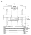
- FIG. 2 is an explanatory diagram showing an example of a cross-sectional structure of the channel resistance.
- a buffer layer 602, an electron supply layer 603, a channel layer 604, an electron supply layer 605, a cap layer (n + layer) 606 are formed on a semiconductor substrate 601 made of a compound semiconductor GaAs by, for example, MOCVD or MBE.
- the electrodes 607 made of ohmic layers are epitaxially grown sequentially.
- the channel resistance is a resistance having the channel layer 604 as a main resistance component and has a positive temperature characteristic.
- FIG. 3 is an explanatory diagram illustrating an example of a cross-sectional structure of the n + resistance.
- a buffer layer 602, an electron supply layer 603, a channel layer 604, an electron supply layer 605, a cap layer (n + layer) 606, and an electrode 607 made of an ohmic layer are sequentially epitaxially grown on the semiconductor substrate 601.
- the n + resistance has a cap layer (n + layer) 606 as a main resistance component.
- the cap layer 606 is formed of an n + -type GaAs layer, and is doped with impurity ions (for example, silicon ions) having n-type conductivity.
- the n + resistance has a lower resistivity per unit area than the channel resistance. Therefore, when realizing the resistance of predetermined resistance value at n + resistor, generally, n + resistance layout area is larger than the channel resistance.
- the n + resistance has a positive temperature characteristic, and its temperature coefficient is smaller than the channel resistance.
- FIG. 4 is an explanatory diagram showing an example of metal resistance.
- an insulating layer (also referred to as an element isolation implantation region) 701 is formed by performing ion implantation on a semiconductor layer epitaxially grown on the semiconductor substrate 700 by MOCVD or MBE. Then, a metal layer 702 and an electrode 703 are sequentially formed on the insulating layer 701.
- the electrode 703 is, for example, Au.
- the metal layer 702 is, for example, WSiN or Ta—SiO 2 .
- the metal resistance is a resistance having the metal layer 702 as a main resistance component and has a negative temperature characteristic.
- FIG. 5 is an explanatory diagram showing another example of metal resistance.
- a semiconductor layer 704 is epitaxially grown on a semiconductor substrate 700 by MOCVD or MBE, and an interlayer oxide film (SiO 2 or the like) 705 is formed thereon.
- an interlayer oxide film (SiO 2 or the like) 705 is formed thereon.
- a metal layer 702 and an electrode 703 are sequentially formed on the interlayer oxide film 705. Similar to FIG. 4, the metal resistance has the metal layer 702 as a main resistance component and has negative temperature characteristics.
- a channel resistance or n + resistance having a positive temperature characteristic is used for the resistor Ra1
- a metal resistance having a negative temperature characteristic is used for the resistor Ra2.
- the temperature fluctuation of the resistance value of the resistance circuit Ra can be reduced.
- Either a channel resistance or an n + resistance may be used as the resistor Ra1, but it is advantageous in terms of characteristics to use a channel resistance.
- FIG. 6 is an explanatory diagram showing an example of temperature characteristics of channel resistance and metal resistance.
- the resistance value at other temperatures is shown with the resistance value at room temperature (25 ° C.) as the reference value (“1.0”).
- reference numeral 801 represents the temperature characteristic of the channel resistance
- reference numeral 802 represents the temperature characteristic of the metal resistance
- Reference numeral 803 represents the temperature characteristic of the combined resistance of the channel resistance and the metal resistance.
- the absolute value of the temperature coefficient of the channel resistance and the temperature coefficient of the metal resistance made of WSiN or Ta—SiO 2 are approximately the same.
- the resistance values of the resistance Ra1 and the resistance Ra2 are preferably the same. Since the resistance value per unit area of the channel resistance is several hundred ⁇ and the resistance value per unit area of the metal resistance is several k ⁇ , in order to form the resistors Ra1 and Ra2 having the same resistance value, If it is a width, the resistance Ra1 (channel resistance) needs to be about 10 times as long as the resistance Ra2 (metal resistance), and if it is the same length, the resistance Ra2 needs about 10 times the width of the resistance Ra1. It becomes.
- the resistor circuit Ra can be realized by laying out the resistors Ra1 and Ra2 separately on the semiconductor substrate as shown in FIGS. 2 to 5 and connecting the respective electrodes in parallel. It is also possible to form the upper and lower layers on the substrate.
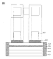
- FIG. 7 shows an example of a method for forming the resistors Ra1 and Ra2.
- a channel resistance is formed by sequentially epitaxial growth in the same manner as in FIG. 2 described above, and this is designated as a resistance Ra1.
- a metal layer 702 is formed between the electrodes 607 at both ends of the channel resistance, and this is defined as a resistance Ra2.
- An interlayer insulating layer 706 is formed between the metal resistance and the channel resistance to insulate the semiconductor layers.
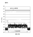
- FIG. 8A and 8B are explanatory diagrams showing an example of the harmonic characteristics of the RF transmission signal in the antenna switch when the resistor circuit Ra is configured only by a resistor having a positive temperature characteristic.
- the harmonic distortion of the RF transmission signal at room temperature is sufficiently low with respect to the required standard value.
- reference numeral 502 in FIG. 8B at high temperatures, spike-like noise occurs at the rise of the RF transmission signal, and the harmonic distortion of the RF transmission signal has a small margin with respect to the required standard value. It is understood. As described above, the deterioration of the characteristics at high temperature is caused by the RF transmission signal leaking to the reception terminal Rx side when the RF transmission signal rises without the FET of the high-frequency switch SW1 being in a sufficiently reverse bias state.
- the antenna switch 1 As indicated by the reference numeral 503 in the figure, spike-like noise does not occur even when the RF transmission signal rises even at a high temperature. This is because, by using the resistor Ra1 having a positive temperature characteristic and the resistor Ra2 having a negative temperature characteristic for the resistor circuit Ra, the temperature variation of the entire resistance value of the resistor circuit Ra can be suppressed, and as a result, the capacitance C2 This is because the temperature fluctuation of the charging time of the battery is suppressed. That is, according to the antenna switch 1, if the optimum charging time in which the field effect transistors M1 and M2 on the receiving side are sufficiently reverse-biased at room temperature is determined, the charging time varies greatly depending on the temperature.
- an antenna switch with high distortion characteristics can be provided, so that the burden of distortion characteristics of other components other than the antenna switch in the distortion characteristics of the entire system that performs wireless communication such as a portable terminal can be reduced. Can do.
- FIG. 10 is a circuit diagram showing a configuration of the antenna switch according to the second embodiment.
- the antenna switch 2 shown in the figure is an SPDT type antenna switch, and establishes, for example, a signal path of a GSM RF signal on the transmission side and the reception side.
- the antenna switch 2 is formed on one compound semiconductor substrate having a high electron mobility such as GaAs.
- the antenna switch 2 includes a reception-side high-frequency switch SW1, a transmission-side high-frequency switch SW2, and a voltage generation circuit 20.
- circuit elements similar to those of the antenna switch 1 according to the first embodiment are denoted by the same reference numerals, and detailed description thereof is omitted.
- the gates of the field effect transistors M1 and M2 in the high frequency switch SW1 on the receiving side are driven by the control voltage V_Rxc supplied to the control terminal Rxc.
- the gate of the field effect transistor M3 in the high frequency switch SW2 on the transmission side is driven by the voltage generated by the voltage generation circuit 20.
- the voltage generation circuit 20 is a booster circuit that generates a positive voltage based on the RF transmission signal supplied to the transmission terminal Tx and the control voltage V_Txc supplied to the control terminal Txc, and outputs the positive voltage to the high-frequency switch SW1 on the transmission side.
- the voltage generation circuit 20 includes capacitors C11 and C12, diodes D3 and D4, a resistor circuit Rb, and resistors R4 and R5, and their connection relations are as follows.
- One end of the capacitor C11 is connected to a node to which the drain of the field effect transistor M3 and the capacitor C3 are connected, and the other end is connected to the resistor circuit Rb.
- the resistor circuit Rb is a circuit in which, for example, a resistor Rb1 and a resistor Rb2 are connected in parallel.
- One end of the resistor circuit Rb is connected to the capacitor C11, and the other end is connected to the anode of the diode D4 and the cathode of the diode D3.
- the anode of the diode D3 is connected to one end of the capacitor C12 and the control terminal Txc, and the cathode of the diode D4 is connected to the other end of the capacitor C12 and to one end of the resistor R5.
- the other end of the resistor R5 is connected to the gate of the field effect transistor M3 through the resistor Rg3.
- One end of the resistor R4 is connected to the control terminal Txc, and the other end is connected to the other end of the resistor R5.
- the voltage generation circuit 20 specifically operates as follows. Consider a case in which, for example, 0V is supplied to the control terminal Rxc as the control voltage V_Rxc, and 3V, for example, is supplied to the control terminal Txc as the control voltage V_Txc. In this case, first, 3 V is applied to the gate of the field effect transistor M3 of the high-frequency switch SW2 on the transmission side via the resistor R4 and the gate resistor Rg3. As a result, the gate and the source of the field effect transistor M3 are forward-biased, and the field effect transistor M3 is turned on. At this time, the source potential (antenna terminal side potential) Vant of the field effect transistor M3 increases following the gate potential, for example, 2.5V.
- the diode D4 when the voltage amplitude of the RF transmission signal is smaller than the control voltage V_Txc, the diode D4 is reverse-biased and becomes non-conductive, and the diode D3 is forward-biased and becomes conductive. For this reason, a current flows from the control terminal Txc to the transmission terminal Tx side via the diode D3, the resistance circuit Rb, and the capacitor C11. At this time, positive charges are stored in the electrode on the resistance circuit Rb side of the capacitor C11.
- the diode D3 when the voltage amplitude of the RF transmission signal is larger than the control voltage V_Txc, the diode D3 is reverse-biased and becomes non-conductive, and the diode D4 is forward-biased and becomes conductive.
- the temperature dependency of the resistor circuit Rb affects the charging time of the capacitor C12. Therefore, if the temperature dependency of the resistance circuit Rb is high, the time during which the gate voltage and the source voltage of the transmission-side field effect transistor M3 rise at a high temperature or a low temperature increases compared to that at normal temperature, and the electric field on the reception side The time until the effect transistors M1 and M2 are sufficiently reverse-biased also increases. Therefore, in the antenna switch 2 according to the second embodiment, similarly to the resistance circuit Ra of the antenna switch 1, a channel resistance or n + resistance having a positive temperature characteristic is used for the resistance Rb1 in the resistance circuit Rb, and the resistance Rb2 is negative.
- a metal resistor having temperature characteristics is used. Thereby, the temperature fluctuation of the entire resistance value of the resistance circuit Rb can be reduced. Further, in order to further suppress the temperature fluctuation, the resistance values of the resistor Rb1 and the resistor Rb2 are set to the same resistance value, for example. Either a channel resistor or an n + resistor may be used for the resistor Rb1, but for the same reason as described above, it is advantageous in terms of characteristics to use a channel resistor.
- an appropriate charging time for the capacitor C12 in which the field-effect transistor M3 on the transmitting side is sufficiently forward biased is determined at room temperature, it depends on the temperature. Since the charging time does not change greatly, it is possible to prevent a leakage path from being formed on the receiving terminal Rx side even at a low temperature or a high temperature, similar to the antenna switch 1, and the harmonic distortion. The deterioration of the characteristics can be prevented. Further, as in the first embodiment, it is possible to reduce the burden of distortion characteristics of other components other than the antenna switch in the distortion characteristics of the entire system that performs wireless communication.
- the present invention is not limited to this, and the resistance of the positive temperature characteristic and the negative temperature are reduced so that the temperature variation of the entire resistance value of the resistor circuit Ra is reduced.
- the resistors Ra1 and Ra2 may be connected in series. The same applies to the resistor circuit Rb.
- the first embodiment exemplifies a case where a resistance circuit Ra having a small temperature variation is applied to the antenna switch 1 including the voltage generation circuit 10 that generates the gate voltages of the field effect transistors M1 and M2 on the receiving side.
- the resistance circuit Rb having a small temperature variation is applied to the antenna switch 2 including the voltage generation circuit 20 that generates the gate voltage of the field effect transistor M3 on the transmission side is illustrated, but the present invention is not limited thereto.
- the voltage generation circuit 10 generates the gate drive voltages of the field-effect transistors M1 and M2 on the reception side using a part of the RF transmission signal at the time of signal transmission, it is not limited to this.
- the voltage generation circuit 20 can also generate gate drive voltages for the field-effect transistors M1 and M2 on the reception side using a part of the RF reception signal when receiving the signal.
Landscapes
- Engineering & Computer Science (AREA)
- Computer Networks & Wireless Communication (AREA)
- Signal Processing (AREA)
- Electronic Switches (AREA)
- Transceivers (AREA)
- Waveguide Switches, Polarizers, And Phase Shifters (AREA)
Abstract
温度変動によるアンテナスイッチの特性の悪化を防止する。本半導体装置(1)は、アンテナに接続するためのアンテナ端子(ANT)とRF信号が供給可能にされる複数の外部端子(Rx、Tx)との間に設けられる複数の電界効果トランジスタ(M1~M3)と、電圧生成回路(10)とを有する。前記電圧生成部は、前記複数の外部端子のうち1つの外部端子(Rx)と前記アンテナ端子との間に設けられる電界効果トランジスタ(M1、M2)をオフさせるとき、他の外部端子(Tx)に供給されるRF信号の前記制御信号に対する極性の切り替わりを利用して抵抗回路(Ra)を介して容量(C2)を充電し、その充電電圧と前記制御信号の電圧との和に基づく電圧を、前記ゲート駆動電圧として出力する。前記抵抗回路は、正の温度特性を有する第1抵抗(Ra1)と、負の温度特性を有する第2抵抗(Ra2)とを含む。
Description
本発明は、無線通信システムのためのアンテナスイッチを内蔵する半導体装置に関し、特にアンテナスイッチにおける温度変動に起因した特性の悪化を抑止するための有効な技術に関する。
携帯電話等の無線通信を行うための携帯端末では、1つのアンテナにつながる信号経路を送信側と受信側で切り替えるためにアンテナスイッチが用いられている。携帯端末に用いられるアンテナスイッチは、オン状態の高周波スイッチには低い挿入損失が求められる一方、オフ状態の高周波スイッチには高いアイソレーション特性と低歪特性が求められる。近年、挿入損失の低いアンテナスイッチとして、低いオン抵抗を持つヘテロ接合構造のHEMT(High Electron Mobility Transistor)をスイッチ素子として用いたアンテナスイッチが多く製品化されている。HEMTのような電界効果トランジスタを用いたアンテナスイッチにおいて、オフ状態の電界効果トランジスタのアイソレーション特性を高めるための技術が特許文献1に開示されている。
特許文献1には、RF送信信号の送信時に、昇圧回路がDC制御電圧とRF送信信号とに基づいて前記DC制御電圧よりも大きい正電圧を生成し、その正電圧を送信側の電界効果トランジスタ(nチャネルのHEMT)のゲート制御電圧とするアンテナスイッチが開示されている。このアンテナスイッチによれば、送信時における送信側の電界効果トランジスタのオン抵抗を低くして挿入損失を低減させるとともに、送信側の電界効果トランジスタのゲートを介して受信側の電界効果トランジスタのソース側の電位を高めることで、受信側の電界効果トランジスタの逆バイアス状態を強くし、アイソレーション特性を高めている。
また、同文献には、RF送信信号の送信時に、降圧回路がDC制御電圧とRF送信信号とに基づいて前記DC制御電圧よりも小さい負電圧を生成し、その負電圧を受信側の電界効果トランジスタ(nチャネルのHEMT)のゲート制御電圧とすることで、受信側の電界効果トランジスタのゲート・ショットキー障壁を逆バイアス状態にするアンテナスイッチが開示されている。このアンテナスイッチによれば、上記の昇圧回路と同様に、受信側の電界効果トランジスタの逆バイアス状態を強くし、アイソレーション特性を高めている。
前記昇圧回路及び降圧回路は、チャージポンプ回路のように、送信信号の極性の切り替わりを利用して容量に充電することでDC制御電圧よりも大きい正電圧又はDC制御電圧よりも小さい負電圧を生成する。このような原理で正電圧又は負電圧を生成する回路において、出力電圧が目標とする値になるまでの時間は、主に前記容量の充電時間で決定される。そのため、例えば特許文献1に記載の降圧回路を内蔵するアンテナスイッチにおいて、仮に降圧回路の容量の充電時間が長いとすると、RF送信信号の送信時に、受信側の電界効果トランジスタが十分なオフ状態(逆バイアス状態)になるまでに長い時間を要し、受信側にRF送信信号のリーク経路が形成され、RF送信時の高調波歪の特性が悪化する虞がある。
容量の充電時間は、主に充電される容量と充電経路に存在する抵抗との時定数によって決定される。例えば、特許文献1の図1に示される降圧回路でいえば、主に容量110と抵抗107の時定数によって充電時間が決定される。容量の充電時間を短くするためには充電経路に存在する抵抗の抵抗値をできるだけ小さくする必要があるが、前記抵抗は容量に流れる電流量が許容値を超えないように制限する役割があるため、極端に小さい値とすることはできない。したがって、回路設計を行う際には、容量に流れる電流量が許容量を超えないように制限しつつ、充電時間が短くなるように抵抗値を決定する必要がある。しかしながら、半導体基板に形成される抵抗は、正の温度特性又は負の温度特性を有するため、常温において容量の充電時間が適切な時間となるように抵抗値を決定したとしても、低温又は高温ではその抵抗値が大きくなり、充電時間が長くなってしまう。例えば、常温で送信信号が立ち上がってから所定時間の経過後に受信側の電界効果トランジスタのゲート電圧が例えば-2.0Vになるとした場合、高温では同じ時間が経過しても例えば-1.0Vにしかならず、-2.0Vになるまでにより多くの時間を要してしまう。そのため、常温では問題がなくても、高温又は低温では、RF送信信号が立ち上がった直後は受信側にRF送信信号のリーク経路が形成され、RF送信信号に高調波歪が発生する虞がある。
近年、携帯端末の通信品質の更なる向上が求められており、携帯端末に用いられるアンテナスイッチにも高いスペックが要求されている。そのため、アンテナスイッチにおける温度変動に起因した特性の悪化も無視することができないと本願発明者は考えた。
本発明の目的は、温度変動によるアンテナスイッチの特性の悪化を防止することにある。
本発明の前記並びにその他の目的と新規な特徴は本明細書の記述及び添付図面から明らかになるであろう。
本願において開示される発明のうち代表的なものの概要を簡単に説明すれば下記のとおりある。
すなわち、本半導体装置は、アンテナに接続するためのアンテナ端子とRF信号が供給可能にされる複数の外部端子との間に設けられる複数の電界効果トランジスタと、電圧生成回路とを有する。前記電圧生成部は、前記複数の外部端子のうち1つの外部端子と前記アンテナ端子との間に設けられる電界効果トランジスタをオフさせるとき、他の外部端子に供給されるRF信号の前記制御信号に対する極性の切り替わりを利用して抵抗回路を介して容量を充電し、その充電電圧と前記制御信号の電圧との和に基づく電圧を、前記ゲート駆動電圧として出力する。前記抵抗回路は、正の温度特性を有する第1抵抗と、負の温度特性を有する第2抵抗とを含む。
本願において開示される発明のうち代表的なものによって得られる効果を簡単に説明すれば下記のとおりである。
すなわち、これによれば、温度変動によるアンテナスイッチの特性の悪化を防止することができる。
1.実施の形態の概要
先ず、本願において開示される発明の代表的な実施の形態について概要を説明する。代表的な実施の形態についての概要説明で括弧を付して参照する図面中の参照符号はそれが付された構成要素の概念に含まれるものを例示するに過ぎない。
先ず、本願において開示される発明の代表的な実施の形態について概要を説明する。代表的な実施の形態についての概要説明で括弧を付して参照する図面中の参照符号はそれが付された構成要素の概念に含まれるものを例示するに過ぎない。
〔1〕(降圧回路における抵抗回路に、正の温度特性の抵抗と負の温度特性の抵抗を用いる)
本発明の代表的な実施の形態に係る半導体装置(1)は、アンテナに接続するためのアンテナ端子(ANT)と、RF信号が供給可能にされる複数の外部端子(Rx、Tx)と、前記アンテナ端子と夫々の前記外部端子との間に設けられる複数の電界効果トランジスタ(M1~M3)と、夫々の前記電界効果トランジスタのオン・オフを制御するための制御信号を入力するための制御端子(Txc、Rxc)とを有する。前記半導体装置は更に、前記複数の外部端子のうち1つの外部端子(Rx)と前記アンテナ端子との間に設けられる電界効果トランジスタ(M1、M2)のゲート駆動電圧を生成する電圧生成部(10)と、を有する。前記電圧生成部は、前記1つの外部端子と前記アンテナ端子との間に設けられる電界効果トランジスタ(M1、M2)をオフさせるとき、他の外部端子(Tx)に供給されるRF信号(RF送信信号)の前記制御信号に対する極性の切り替わりを利用して、抵抗回路(Ra)を介して容量(C2)を充電し、その充電電圧と前記制御信号の電圧(V_Rxc)との和に基づく電圧を、前記ゲート駆動電圧として出力する。また、前記抵抗回路は、正の温度特性を有する第1抵抗(Ra1)と、負の温度特性を有する第2抵抗(Ra2)とを含む。
本発明の代表的な実施の形態に係る半導体装置(1)は、アンテナに接続するためのアンテナ端子(ANT)と、RF信号が供給可能にされる複数の外部端子(Rx、Tx)と、前記アンテナ端子と夫々の前記外部端子との間に設けられる複数の電界効果トランジスタ(M1~M3)と、夫々の前記電界効果トランジスタのオン・オフを制御するための制御信号を入力するための制御端子(Txc、Rxc)とを有する。前記半導体装置は更に、前記複数の外部端子のうち1つの外部端子(Rx)と前記アンテナ端子との間に設けられる電界効果トランジスタ(M1、M2)のゲート駆動電圧を生成する電圧生成部(10)と、を有する。前記電圧生成部は、前記1つの外部端子と前記アンテナ端子との間に設けられる電界効果トランジスタ(M1、M2)をオフさせるとき、他の外部端子(Tx)に供給されるRF信号(RF送信信号)の前記制御信号に対する極性の切り替わりを利用して、抵抗回路(Ra)を介して容量(C2)を充電し、その充電電圧と前記制御信号の電圧(V_Rxc)との和に基づく電圧を、前記ゲート駆動電圧として出力する。また、前記抵抗回路は、正の温度特性を有する第1抵抗(Ra1)と、負の温度特性を有する第2抵抗(Ra2)とを含む。
項1の半導体装置によれば、前記容量の充電時間を決定する前記抵抗回路の温度依存性が低くなるから、オフさせる電界効果トランジスタが深い逆バイアス状態に移行するまでに要する時間の温度変動を小さくすることができる。これにより、例えば、低温状態又は高温状態において、信号の送信と受信を切り替えた直後に、オフ状態の電界効果トランジスタを経由するRF信号のリーク経路の形成を防止することができ、高周波歪の特性の悪化を防止することができる。
〔2〕(エピタキシャル成長によって形成された半導体層を用いた抵抗と、金属抵抗)
項1の半導体装置において、前記第1抵抗は半導体基板にエピタキシャル成長によって形成された半導体層(チャネル層604、又はキャップ層606)を用いた抵抗であり、前記第2抵抗は金属層(702(WSiN、Ta-SiO2))を用いた抵抗である。
項1の半導体装置において、前記第1抵抗は半導体基板にエピタキシャル成長によって形成された半導体層(チャネル層604、又はキャップ層606)を用いた抵抗であり、前記第2抵抗は金属層(702(WSiN、Ta-SiO2))を用いた抵抗である。
これによれば、容易に前記抵抗回路の抵抗値の温度変動を小さくすることができる。
〔3〕(第1抵抗と第2抵抗は層間絶縁層を挟んで上下に形成される)
項2の半導体装置において、前記第1抵抗と前記第2抵抗とは、半導体層間を絶縁するための絶縁層(706)を挟んで上下に対向して配置される。
項2の半導体装置において、前記第1抵抗と前記第2抵抗とは、半導体層間を絶縁するための絶縁層(706)を挟んで上下に対向して配置される。
これによれば、半導体基板上に前記第1抵抗と前記第2抵抗を並べてレイアウト配置する場合に比べて、チップ面積をより低減することができる。
〔4〕(半導体層はチャネル抵抗)
項2又は3の半導体装置において、前記半導体基板は化合物半導体(GaAs)からなる。また、前記半導体基板にエピタキシャル成長によって形成された半導体層はチャネル層(604)であり、前記金属層は、WSiN、又はTa-SiO2である。
項2又は3の半導体装置において、前記半導体基板は化合物半導体(GaAs)からなる。また、前記半導体基板にエピタキシャル成長によって形成された半導体層はチャネル層(604)であり、前記金属層は、WSiN、又はTa-SiO2である。
例えば化合物半導体(GaAs)に形成されるチャネル層の温度係数と金属層の温度係数の絶対値は、同程度の値となるため、項4によれば、前記抵抗回路の抵抗値の温度変動をより小さくすることができる。
〔5〕(受信側のFETのゲート駆動電圧を生成)
項1乃至4のいずれかの半導体装置において、前記1つの外部端子はRF信号を受信するための受信端子(Rx)であり、前記他の外部端子はRF信号を送信するための送信端子(Tx)である。
項1乃至4のいずれかの半導体装置において、前記1つの外部端子はRF信号を受信するための受信端子(Rx)であり、前記他の外部端子はRF信号を送信するための送信端子(Tx)である。
〔6〕(昇圧回路における抵抗回路に、正の温度特性の抵抗と負の温度特性の抵抗を用いる)
本発明の代表的な別の実施の形態に係る半導体装置(2)は、アンテナに接続するためのアンテナ端子(ANT)と、RF信号が供給可能にされる複数の外部端子(Rx、Tx)と、前記アンテナ端子と夫々の前記外部端子との間に設けられる複数の電界効果トランジスタ(M1~M3)と、夫々の前記電界効果トランジスタのオン・オフを制御するための制御信号を入力するための制御端子(Rxc、Txc)とを有する。前記半導体装置は更に、前記複数の外部端子のうち1つの外部端子(Tx)と前記アンテナ端子との間に設けられる電界効果トランジスタ(M3)のゲート駆動電圧を生成する電圧生成部(20)を有する。前記電圧生成部は、前記1つの外部端子と前記アンテナ端子との間に設けられる電界効果トランジスタ(M3)をオンさせるとき、前記1つの外部端子に供給されるRF信号(RF送信信号)の前記制御信号に対する極性の切り替わりを利用して抵抗回路(Rb)を介して容量(C12)を充電し、その充電電圧と前記制御信号の電圧との和に基づく電圧を、前記ゲート駆動電圧として出力する。また、前記抵抗回路は、正の温度特性を有する第1抵抗(Rb1)と、負の温度特性を有する第2抵抗(Rb2)とを含む。
本発明の代表的な別の実施の形態に係る半導体装置(2)は、アンテナに接続するためのアンテナ端子(ANT)と、RF信号が供給可能にされる複数の外部端子(Rx、Tx)と、前記アンテナ端子と夫々の前記外部端子との間に設けられる複数の電界効果トランジスタ(M1~M3)と、夫々の前記電界効果トランジスタのオン・オフを制御するための制御信号を入力するための制御端子(Rxc、Txc)とを有する。前記半導体装置は更に、前記複数の外部端子のうち1つの外部端子(Tx)と前記アンテナ端子との間に設けられる電界効果トランジスタ(M3)のゲート駆動電圧を生成する電圧生成部(20)を有する。前記電圧生成部は、前記1つの外部端子と前記アンテナ端子との間に設けられる電界効果トランジスタ(M3)をオンさせるとき、前記1つの外部端子に供給されるRF信号(RF送信信号)の前記制御信号に対する極性の切り替わりを利用して抵抗回路(Rb)を介して容量(C12)を充電し、その充電電圧と前記制御信号の電圧との和に基づく電圧を、前記ゲート駆動電圧として出力する。また、前記抵抗回路は、正の温度特性を有する第1抵抗(Rb1)と、負の温度特性を有する第2抵抗(Rb2)とを含む。
項6の半導体装置によれば、前記容量の充電時間を決定する前記抵抗回路の温度依存性が低くなるから、オンさせる電界効果トランジスタが深い順バイアス状態に移行するまでに要する時間の温度変動を小さくすることができる。一方、オンさせる電界効果トランジスタのゲート電圧に追従してアンテナ端子を介して接続される他の電界効果トランジスタ(例えば、オフ状態の電界効果トランジスタ)のソース電圧も変化するため、前記他の電界効果トランジスタのゲート・ソース間が深い逆バイアス状態に移行するまでに要する時間の温度変動も小さくすることができる。したがって、例えば低温状態や高温状態において、信号の送信と受信を切り替えた直後に、オフ状態の電界効果トランジスタを経由したRF信号のリーク経路の形成を防止することができ、高周波歪の悪化を防止することができる。
〔7〕(エピタキシャル成長によって形成された半導体層を用いた抵抗と金属抵抗)
項6の半導体装置において、前記第1抵抗は、半導体基板にエピタキシャル成長によって形成された半導体層(チャネル層604、又はキャップ層606)を用いた抵抗であり、前記第2抵抗は、金属層(702(WSiN、Ta-SiO2))を用いた抵抗である。
項6の半導体装置において、前記第1抵抗は、半導体基板にエピタキシャル成長によって形成された半導体層(チャネル層604、又はキャップ層606)を用いた抵抗であり、前記第2抵抗は、金属層(702(WSiN、Ta-SiO2))を用いた抵抗である。
これによれば、半導体装置において容易に前記抵抗回路の抵抗値の温度変動を小さくすることができる。
〔8〕(第1抵抗と第2抵抗は層間絶縁層を挟んで上下に形成される)
項7の半導体装置において、前記第1抵抗と前記第2抵抗とは、半導体層間を絶縁するための絶縁層(706)を挟んで上下に対向して配置される。
項7の半導体装置において、前記第1抵抗と前記第2抵抗とは、半導体層間を絶縁するための絶縁層(706)を挟んで上下に対向して配置される。
これによれば、半導体基板上に前記第1抵抗と前記第2抵抗を並べてレイアウト配置する場合に比べて、チップ面積をより低減することができる。
〔9〕(半導体層はチャネル抵抗)
項7又は8の半導体装置において、前記半導体基板は化合物半導体(GaAs)からなる。また、前記半導体基板にエピタキシャル成長によって形成された半導体層はチャネル層(604)であり、前記金属層は、WSiN、又はTa-SiO2である。
項7又は8の半導体装置において、前記半導体基板は化合物半導体(GaAs)からなる。また、前記半導体基板にエピタキシャル成長によって形成された半導体層はチャネル層(604)であり、前記金属層は、WSiN、又はTa-SiO2である。
例えば化合物半導体(GaAs)に形成されるチャネル層の温度係数と金属層の温度係数の絶対値は、同程度の値となるため、項9によれば、前記抵抗回路の抵抗値の温度変動をより小さくすることができる。
〔10〕(送信側のFETのゲート駆動電圧を生成)
項6乃至9のいずれかの半導体装置において、前記1つの外部端子はRF信号を送信するための送信端子(Tx)である。
項6乃至9のいずれかの半導体装置において、前記1つの外部端子はRF信号を送信するための送信端子(Tx)である。
〔11〕(電圧生成回路(昇圧/降圧含む)における抵抗回路に、正の温度特性の抵抗と負の温度特性の抵抗を用いる)
本発明の代表的な別の実施の形態に係る半導体装置(1、2)は、アンテナに接続するためのアンテナ端子(ANT)と、RF信号が供給可能にされる複数の外部端子(Rx、Tx)と、前記アンテナ端子と夫々の前記外部端子との間に設けられる複数の電界効果トランジスタ(M1~M3)と、夫々の前記電界効果トランジスタのオン・オフを制御するための制御信号を入力するための制御端子(Txc、Rxc)とを有する。前記半導体装置は更に、前記複数の外部端子のうち1つの外部端子(Rx又はTx)と前記アンテナ端子との間に設けられる電界効果トランジスタ(M1及びM2、又はM3)のゲート駆動電圧を生成する電圧生成部(10、20)を有する。前記電圧生成部は、オン状態とされる電界効果トランジスタ(M3)のソース又はドレインに供給される送信信号(RF送信信号)の前記制御信号に対する極性の切り替わりを利用して、抵抗回路(Ra、Rb)を介して容量(C2、C12)を充電し、その充電電圧と前記制御信号の電圧との和に基づく電圧を前記ゲート駆動電圧として出力する。また、前記抵抗回路は、正の温度特性を有する第1抵抗(Ra1、Rb1)と、負の温度特性を有する第2抵抗(Ra2、Rb2)とを含む。
本発明の代表的な別の実施の形態に係る半導体装置(1、2)は、アンテナに接続するためのアンテナ端子(ANT)と、RF信号が供給可能にされる複数の外部端子(Rx、Tx)と、前記アンテナ端子と夫々の前記外部端子との間に設けられる複数の電界効果トランジスタ(M1~M3)と、夫々の前記電界効果トランジスタのオン・オフを制御するための制御信号を入力するための制御端子(Txc、Rxc)とを有する。前記半導体装置は更に、前記複数の外部端子のうち1つの外部端子(Rx又はTx)と前記アンテナ端子との間に設けられる電界効果トランジスタ(M1及びM2、又はM3)のゲート駆動電圧を生成する電圧生成部(10、20)を有する。前記電圧生成部は、オン状態とされる電界効果トランジスタ(M3)のソース又はドレインに供給される送信信号(RF送信信号)の前記制御信号に対する極性の切り替わりを利用して、抵抗回路(Ra、Rb)を介して容量(C2、C12)を充電し、その充電電圧と前記制御信号の電圧との和に基づく電圧を前記ゲート駆動電圧として出力する。また、前記抵抗回路は、正の温度特性を有する第1抵抗(Ra1、Rb1)と、負の温度特性を有する第2抵抗(Ra2、Rb2)とを含む。
これによれば、前記容量の充電時間の温度変動を低減することができるから、前記1つの外部端子と前記アンテナ端子との間に設けられる電界効果トランジスタの前記ゲート駆動電圧が目標とする電圧になるまでの時間の温度変動を小さくすることができる。これにより、当該電界効果トランジスタが目標とするバイアス状態へ移行するまでに要する時間の温度依存性を低くすることができ、温度変動に伴う電界効果トランジスタのバイアス状態の変化に起因するアンテナスイッチの特性悪化を防止することができる。
〔12〕(受信側のFETのゲート駆動電圧を生成)
項11の半導体装置において、前記1つの外部端子は受信信号が供給可能にされる受信端子(Rx)である。
項11の半導体装置において、前記1つの外部端子は受信信号が供給可能にされる受信端子(Rx)である。
項11の半導体装置によれば、受信側の電界効果トランジスタのゲート・ソース間が深い逆バイアス状態に移行するまでに要する時間の温度変動が抑えられる。これにより、例えば、低温状態や高温状態において、信号の送信と受信を切り替えた直後に、オフ状態の受信側の電界効果トランジスタを経由したRF信号のリーク経路の形成を防止することができ、高周波歪の特性の悪化を防止することができる。
〔13〕(送信側のFETのゲート駆動電圧を生成)
項11の半導体装置において、前記1つの外部端子は送信信号が供給可能にされる送信端子(Tx)である。
項11の半導体装置において、前記1つの外部端子は送信信号が供給可能にされる送信端子(Tx)である。
項13の半導体装置によれば、送信側の電界効果トランジスタのゲートを介して他の電界効果トランジスタ(例えばオフ状態の受信側の電界効果トランジスタ)のゲート・ソース間が深い逆バイアス状態に移行するまでに要する時間の温度変動が抑えられる。これにより、例えば、低温状態や高温状態において、信号の送信と受信を切り替えた直後に、オフ状態の受信側の電界効果トランジスタを経由したRF信号のリーク経路の形成を防止することができ、高周波歪の特性の悪化を防止することができる。
2.実施の形態の詳細
実施の形態について更に詳述する。
実施の形態について更に詳述する。
≪実施の形態1≫
図1は、実施の形態1に係るアンテナスイッチの構成を示す回路図である。
図1は、実施の形態1に係るアンテナスイッチの構成を示す回路図である。
同図に示されるアンテナスイッチ1は、シングルポール2スロー(SPDT:Single pole Double throw)型のアンテナスイッチであり、例えば、GSM(Global System for Mobile Communications)(登録商標)方式のRF信号の信号経路を送信側と受信側で確立する。特に制限されないが、アンテナスイッチ1は、GaAsのような高い電子移動度を有する1個の化合物半導体基板に形成される。アンテナスイッチ1は、具体的に、受信側の高周波スイッチSW1、送信側の高周波スイッチSW2、及び電圧生成回路10を含んで構成される。
受信側の高周波スイッチSW1は、制御端子Rxcに供給された制御電圧V_Rxcに応じて、アンテナに接続するためのアンテナ端子ANTとRF受信信号が供給される受信端子Rxとの間の接続と遮断を切り替える。高周波スイッチSW1は、例えばnチャネルのHEMTであるM1、M2を2個直列に接続したマルチゲート構造の電界効果トランジスタを有する。マルチゲート構造のHEMTを用いることにより、高周波スイッチSW1で扱うことができる電圧を増大させるとともに、電界効果トランジスタM1、M2での損失が小さくなるように低いオン抵抗を確保することができる。電界効果トランジスタM1、M2の夫々のドレイン・ソース間には、比較的高い抵抗値(例えば、数十kΩ)の抵抗Rd1、Rd2が接続される。これにより、電界効果トランジスタM1、M2がオフしているときに、ドレイン電圧とソース電圧を等しくすることができる。電界効果トランジスタM1、M2のゲートは、夫々のゲートに接続されるゲート抵抗Rg1、Rg2を介して電圧生成回路10の抵抗R2に接続される。ゲート抵抗Rg1、Rg2の抵抗値を比較的高い抵抗値とすることで、制御端子RxcにRF信号が漏れることによる損失を低減させることができる。
高周波スイッチSW2は、制御端子Txcに供給された制御電圧V_Txcに応じて、アンテナ端子ANTとRF送信信号が供給される送信端子Txとの間の接続と遮断を切り替える。高周波スイッチSW2は、例えば1つのnチャネルのHEMTから構成される電界効果トランジスタM3を有する。電界効果トランジスタM3のドレイン・ソース間には、高周波スイッチSW1と同様に、比較的高い抵抗値(例えば、数十kΩ)の抵抗Rd3が接続される。また、電界効果トランジスタM3のゲートは、ゲート抵抗Rg3、Rg4を介して制御端子Txcに接続される。ゲート抵抗Rg3、Rg4の抵抗値を比較的高い抵抗値とすることで、制御端子TxcにRF信号が漏れることによる損失を低減させることができる。
送信端子Txと電界効果トランジスタM3との間に容量C3が挿入され、電界効果トランジスタM2とM3が接続されるノードとアンテナ端子ANTとの間に容量C4が挿入され、受信端子Rxと電界効果トランジスタM1との間に容量C5が挿入される。夫々の容量C3~C5は、当該容量の一端に接続される外部端子(アンテナ端子、受信端子、又は送信端子)にDC電位が印加されるのを防止するためのDCカット機能と、RF信号を通過させるためのACカップリング機能を持つ。
電圧生成回路10は、送信端子Txに供給されるRF送信信号と制御端子Rxcに供給された制御電圧V_Rxcに基づいて負電圧を生成し、受信側の高周波スイッチSW1に出力する降圧回路である。具体的に、電圧生成回路10は、容量C1、C2、ダイオードD1、D2、抵抗回路Ra、及び抵抗R2、R3から構成され、夫々の接続関係は以下である。容量C1の一端は、電界効果トランジスタM3のドレインと容量C3が接続されるノードに接続され、他端は抵抗回路Raに接続される。抵抗回路Raの一端が容量C1に接続され、他端がダイオードD1のアノード及びダイオードD2のカソードに接続される。ダイオードD1のカソードは容量C2の一端に接続され、ダイオードD2のアノードは前記容量C2の他端に接続される。容量C2の前記一端及びダイオードD1のカソードは制御端子Rxcに接続される。また、抵抗R2の一端は制御端子Rxcに接続され、他端は抵抗R3の一端及び電界効果トランジスタM1、M2のゲート抵抗Rg1、Rg2に接続される。抵抗R3の他端は、容量C2の前記他端及びダイオードD2のアノード側に接続される。
ここで、アンテナスイッチ1を送信モードに切り替えるために、制御端子Rxcに制御電圧V_Rxcとして例えば0Vが供給され、制御端子Txcに制御電圧V_Txcとして例えば3Vが供給される場合を考える。この場合、送信側の電界効果トランジスタM3はオン状態となり、電界効果トランジスタM3のソース電位(アンテナ端子側の電位)Vantはゲート電位に追従して上昇し、その値は例えば2.5Vとなる。また、受信側の電界効果トランジスタM1、M2のゲート・ソース間は逆バイアスされ、電界効果トランジスタM1、M2はオフ状態となる。この状態で送信端子TxにRF送信信号が入力されると、RF送信信号は高周波スイッチSW2を介してアンテナ端子ANTに伝達される。また、RF送信信号の一部は電圧生成回路10に入力される。
例えば、RF送信信号が制御電圧V_Rxcよりも大きい電圧振幅(正の電圧振幅)となったとき、ダイオードD2は逆バイアスされて非導通状態となり、ダイオードD1は順バイアスされて導通状態となる。これにより、送信端子Tx側から容量C1、抵抗回路Ra及びダイオードD1を介して制御端子Rxcに電流が流れ込み、容量C1の抵抗回路Ra側の電極に負の電荷が蓄えられる。次に、RF信号が制御電圧V_Rxcよりも小さい電圧振幅(負の電圧振幅)となったとき、ダイオードD1は逆バイアスされて非導通状態となり、ダイオードD2は順バイアスされて導通状態となる。これにより、制御端子Rxcから容量C2、ダイオードD2、抵抗回路Ra、容量C1を介して送信端子Tx側に電流が流れ込み、容量C1の抵抗Ra側の電極に蓄えられていた負の電荷が、容量C2のダイオードD2側の電極に移動して蓄えられる。以上のようにRF送信信号の極性が制御電圧V_Rxc(=0V)に対して交互に切り替わることを利用して、容量C1と容量C2との間で電荷を移動させることで、容量C2の両端子間に、ダイオードD2側の電極を負極性とした電圧(例えば-2.0V)が充電される。この負電圧が受信側の電界効果トランジスタM1、M2のゲート電圧VG12として供給されることで、受信側の電界効果トランジスタM1、M2のゲート・ソース間が深い逆バイアス状態となり、受信側の高周波スイッチSW1のアイソレーション特性を向上させることができる。
抵抗回路Raは、例えば抵抗Ra1及び抵抗Ra2の2つの抵抗が並列接続された回路構成とされる。以下、抵抗Ra1及び抵抗Ra2について詳細に説明する。
アンテナスイッチ1における抵抗として、化合物半導体GaAsからなる半導体基板上に、例えば有機金属気相成長(MOCVD:Metalorganic chemical vapor deposition)やMBE(Molecular Beam Epitaxy)等により形成されたチャネル層、キャップ層、及び金属層を用いることができる。以下、チャネル層を用いた抵抗をチャネル抵抗と称し、キャップ層(n+層)を用いた抵抗をn+抵抗と称し、金属層を用いた抵抗を金属抵抗と称する。
図2は、チャネル抵抗の断面構造の一例を示す説明図である。同図に示されるように、化合物半導体GaAsからなる半導体基板601に、例えばMOCVDやMBEにより、バッファ層602、電子供給層603、チャネル層604、電子供給層605、キャップ層(n+層)606、オーミック層からなる電極607が順次エピタキシャル成長される。チャネル抵抗は、チャネル層604を主な抵抗成分とする抵抗であり、正の温度特性を有する。
図3は、n+抵抗の断面構造の一例を示す説明図である。図2と同様に、半導体基板601に、バッファ層602、電子供給層603、チャネル層604、電子供給層605、キャップ層(n+層)606、オーミック層からなる電極607が順次エピタキシャル成長される。n+抵抗は、キャップ層(n+層)606を主な抵抗成分とする。キャップ層606は、n+型GaAs層から形成され、n型の導電型を有する不純物イオン(例えば、シリコンイオン)がドープされている。n+抵抗はチャネル抵抗に比べて単位面積当たりの抵抗率が低い。したがって、所定の抵抗値の抵抗をn+抵抗で実現する場合、一般に、n+抵抗はチャネル抵抗に比べてレイアウト面積が大きくなる。また、n+抵抗は正の温度特性を有し、その温度係数はチャネル抵抗に比べて小さい。
図4は、金属抵抗の一例を示す説明図である。同図に示されるように、半導体基板700上にMOCVDやMBEによってエピタキシャル成長された半導体層にイオン注入を行うことで絶縁層(素子分離注入領域、とも称する)701が形成される。そして、絶縁層701の上に金属層702と電極703が順次形成される。電極703は、例えばAu等である。また、金属層702は、例えばWSiNやTa-SiO2である。金属抵抗は、金属層702を主な抵抗成分とする抵抗であり、負の温度特性を有する。
図5は、金属抵抗の別の一例を示す説明図である。同図に示されるように、半導体基板700上にMOCVDやMBEによって半導体層704をエピタキシャル成長させ、その上に層間酸化膜(SiO2等)705を形成する。そして、層間酸化膜705の上に金属層702と電極703が順次形成される。図4と同様に、金属抵抗は金属層702を主な抵抗成分とし、負の温度特性を有する。
アンテナスイッチ1では、抵抗Ra1には正の温度特性を有するチャネル抵抗又はn+抵抗を用い、抵抗Ra2には負の温度特性を有する金属抵抗を用いる。これにより、抵抗回路Raの抵抗値の温度変動を低減することができる。抵抗Ra1としてチャネル抵抗又はn+抵抗のいずれを用いても良いが、チャネル抵抗を用いる方が特性面で有利である。
図6はチャネル抵抗と金属抵抗の温度特性の一例を示す説明図である。同図では、常温(25℃)における抵抗値を基準値(“1.0”)として他の温度における抵抗値の割合を表している。同図において、参照符号801はチャネル抵抗の温度特性を表し、参照符号802は金属抵抗の温度特性を表す。また、参照符号803は、チャネル抵抗と金属抵抗の合成抵抗の温度特性を表す。同図に示されるように、チャネル抵抗の温度係数とWSiNやTa-SiO2からなる金属抵抗の温度係数の絶対値は同程度の値となる。そこで、抵抗Ra1にチャネル抵抗を用いることで、n+抵抗を用いる場合に比べて、抵抗回路Raの抵抗値(抵抗Ra1と抵抗Ra2の合成抵抗の抵抗値)の温度変動をより小さく抑えることが可能となる。
チャネル抵抗及び金属抵抗は、温度係数の絶対値が同程度の値であることから、抵抗Ra1及び抵抗Ra2は同程度の抵抗値が望ましい。チャネル抵抗の単位面積当たりの抵抗値は数百Ωであり、金属抵抗の単位面積当たりの抵抗値は数kΩであるので、同一の抵抗値の抵抗Ra1及び抵抗Ra2を形成するには、同一の幅であれば、抵抗Ra1(チャネル抵抗)は抵抗Ra2(金属抵抗)の約10倍の長さが必要となり、同一の長さであれば、抵抗Ra2は抵抗Ra1の約10倍の幅が必要となる。
抵抗回路Raは、図2~図5のように抵抗Ra1、Ra2を別個に半導体基板上にレイアウト配置し、夫々の電極を並列接続することで実現することができるが、抵抗Ra1、Ra2を半導体基板上に上下に重ねて形成することも可能である。図7に、抵抗Ra1、Ra2の形成方法の一例を示す。
同図に示されるように、前述の図2と同様に順次エピタキシャル成長させることでチャネル抵抗を形成し、それを抵抗Ra1とする。そして、チャネル抵抗の両端の電極607間に金属層702を形成し、それを抵抗Ra2とする。金属抵抗とチャネル抵抗との間には、半導体層間を絶縁するための層間絶縁層706が形成される。このように、抵抗Ra1及び抵抗Ra2を半導体基板上で上下に重ねて形成することで、抵抗Ra1及び抵抗Ra2を並べてレイアウト配置する場合に比べて、チップ面積をより低減することができる。
図8A及び図8Bは、抵抗回路Raを正の温度特性を有する抵抗のみで構成した場合のアンテナスイッチにおけるRF送信信号の高調波特性の一例を示す説明図である。図8Aには、常温(Ta=25℃)においてアンテナスイッチを受信モードから送信モードに切り替えたときのRF送信信号の高調波歪の特性が示される。図8Bには、高温(Ta=90℃)においてアンテナスイッチを受信モードから送信モードに切り替えたときのRF送信信号の高調波歪の特性が示される。
図8Aにおける参照符号501に示されるように、常温におけるRF送信信号の高調波歪は要求される規格値に対して十分低い値となる。他方、図8Bにおける参照符号502に示されるように、高温では、RF送信信号の立ち上がり時にスパイク状のノイズが発生し、RF送信信号の高調波歪は要求される規格値に対する余裕度が小さくなることが理解される。前述したように、高温時の特性の悪化は、RF送信信号の立ち上がり時に、高周波スイッチSW1のFETが十分な逆バイアス状態とならずにRF送信信号が受信端子Rx側に漏れることに起因する。
図9は、実施の形態1に係るアンテナスイッチ1におけるRF送信信号の高調波特性の一例を示す説明図である。同図には、高温(Ta=90℃)においてアンテナスイッチ1を受信モードから送信モードに切り替えたときのRF送信信号の高調波歪の特性が示される。
アンテナスイッチ1によれば、同図の参照符号503に示されるように、高温においてもRF送信信号の立ち上がり時にスパイク状のノイズが発生することはない。これは、抵抗回路Raに正の温度特性を有する抵抗Ra1と負の温度特性を有する抵抗Ra2とを用いることで、抵抗回路Raの全体の抵抗値の温度変動が抑えられ、その結果、容量C2の充電時間の温度変動が抑えられたからである。すなわち、アンテナスイッチ1によれば、常温において受信側の電界効果トランジスタM1、M2が十分な逆バイアス状態となる最適な充電時間を決定しておけば、温度に依存してその充電時間が大きく変化することはないから、低温又は高温であっても、受信端子Rx側にリーク経路が形成されるのを防止することができ、高調波歪の特性の悪化を防止することができる。これにより、高い歪特性のアンテナスイッチを提供することができるから、例えば携帯端末のような無線通信を行うシステム全体の歪特性におけるアンテナスイッチ以外の他の構成部品の歪特性の負担を軽減することができる。
≪実施の形態2≫
図10は、実施の形態2に係るアンテナスイッチの構成を示す回路図である。
図10は、実施の形態2に係るアンテナスイッチの構成を示す回路図である。
同図に示されるアンテナスイッチ2は、SPDT型のアンテナスイッチであり、例えば、GSM方式のRF信号の信号経路を送信側と受信側で確立する。特に制限されないが、アンテナスイッチ2は、GaAsのような高い電子移動度を有する1個の化合物半導体基板に形成される。アンテナスイッチ2は、具体的に、受信側の高周波スイッチSW1、送信側の高周波スイッチSW2、及び電圧生成回路20を含んで構成される。なお、図10において、実施の形態1に係るアンテナスイッチ1と同様の回路要素には同一の符号を付してその詳細な説明を省略する。
受信側の高周波スイッチSW1における電界効果トランジスタM1、M2のゲートは、制御端子Rxcに供給される制御電圧V_Rxcによって駆動される。また、送信側の高周波スイッチSW2における電界効果トランジスタM3のゲートは、電圧生成回路20によって生成された電圧によって駆動される。
電圧生成回路20は、送信端子Txに供給されるRF送信信号と制御端子Txcに供給された制御電圧V_Txcに基づいて正電圧を生成し、送信側の高周波スイッチSW1に出力する昇圧回路である。具体的に、電圧生成回路20は、容量C11、C12、ダイオードD3、D4、抵抗回路Rb、及び抵抗R4、R5から構成され、夫々の接続関係は以下である。容量C11の一端は、電界効果トランジスタM3のドレインと容量C3が接続されるノードに接続され、他端は抵抗回路Rbに接続される。抵抗回路Rbは、例えば抵抗Rb1と抵抗Rb2とが並列接続された回路である。抵抗回路Rbの一端が容量C11に接続され、他端がダイオードD4のアノードとダイオードD3のカソードに接続される。ダイオードD3のアノードは容量C12の一端に接続されるとともに制御端子Txcに接続され、ダイオードD4のカソードは前記容量C12の他端に接続されるとともに抵抗R5の一端に接続される。抵抗R5の他端は抵抗Rg3を介して電界効果トランジスタM3のゲートに接続される。また、抵抗R4の一端は制御端子Txcに接続され、他端は抵抗R5の前記他端に接続される。
電圧生成回路20は具体的に以下のように動作する。制御端子Rxcに制御電圧V_Rxcとして例えば0Vが供給され、制御端子Txcに制御電圧V_Txcとして例えば3Vが供給される場合を考える。この場合、先ず、送信側の高周波スイッチSW2の電界効果トランジスタM3のゲートには抵抗R4及びゲート抵抗Rg3を介して3Vが印加される。これにより、電界効果トランジスタM3のゲート・ソース間が順バイアスされ、電界効果トランジスタM3はオン状態となる。このとき、電界効果トランジスタM3のソース電位(アンテナ端子側の電位)Vantはゲート電位に追従して上昇し、例えば2.5Vとなる。また、受信側の電界効果トランジスタM1、M2のゲートには0Vが印加される。これにより、電界効果トランジスタM1、M2のゲート・ソース間は逆バイアス状態(Vgs=-2.5V)となるから、電界効果トランジスタM1、M2はオフ状態となる。この状態で送信端子RxにRF送信信号が供給されると、RF送信信号は高周波スイッチSW2を介してアンテナ端子ANTに伝達されるとともに、その一部が電圧生成回路20に入力される。例えば、RF送信信号の電圧振幅が制御電圧V_Txcよりも小さい場合、ダイオードD4は逆バイアスされて非導通状態となり、ダイオードD3は順バイアスされて導通状態となる。このため、制御端子TxcからダイオードD3、抵抗回路Rb、及び容量C11を介して送信端子Tx側に電流が流れ込む。このとき、容量C11の抵抗回路Rb側の電極には正の電荷が蓄えられる。次に、RF送信信号の電圧振幅が制御電圧V_Txcよりも大きい場合、ダイオードD3は逆バイアスされて非導通状態となり、ダイオードD4は順バイアスされて導通状態となる。そのため、送信端子Tx側から容量C11、抵抗回路Rb、ダイオードD4、容量C12を介して制御端子Txcに電流が流れ込む。このとき、容量C11の抵抗回路Rb側の電極に蓄えられていた正の電荷が容量C12のダイオードD4側の電極に移動して蓄えられる。以上のようにRF送信信号の極性が制御電圧V_Txc(=3V)に対して交互に切り替わることを利用して、容量C11と容量C12との間で電荷を移動させることで、容量C12の両端子間に、ダイオードD4側の電極を正極性とした電圧(例えば5V)が充電される。この正電圧が送信側の電界効果トランジスタM3のゲート電圧VG3として供給されることで、電界効果トランジスタM3のゲート・ソース間がより深い順バイアス状態となり、送信側のスイッチの挿入損失を低減することができる。更に、電界効果トランジスタM3のゲート電圧が上昇することにより、電界効果トランジスタM3のソース側の電圧も上昇し、その電圧は例えば4.5Vになる。これにより、受信側の電界効果トランジスタM1、M2のソース電位も上昇するから、受信側の電界効果トランジスタM1、M2のゲート・ソース間が深い逆バイアス状態(Vgs=-4.5V)となり、受信側の高周波スイッチSW1のアイソレーション特性を向上させることができる。
前述の電圧生成回路10の抵抗回路Raと同様に、抵抗回路Rbの温度依存性は、容量C12の充電時間に影響する。そのため、抵抗回路Rbの温度依存性が高いと、高温時又は低温時において、送信側の電界効果トランジスタM3のゲート電圧及びソース電圧が上昇する時間が常温時より増加し、また、受信側の電界効果トランジスタM1、M2が十分な逆バイアス状態となるまでの時間も増加することになる。そこで、実施の形態2に係るアンテナスイッチ2では、アンテナスイッチ1の抵抗回路Raと同様に、抵抗回路Rbにおける抵抗Rb1に正の温度特性を有するチャネル抵抗又はn+抵抗を用い、抵抗Rb2に負の温度特性を有する金属抵抗を用いる。これにより、抵抗回路Rbの全体の抵抗値の温度変動を低減することができる。また、より温度変動を抑えるため、抵抗Rb1と抵抗Rb2の抵抗値は、例えば同一の抵抗値とされる。抵抗Rb1にチャネル抵抗又はn+抵抗のいずれを用いても良いが、前述と同様の理由から、チャネル抵抗を用いる方が特性面で有利である。
以上、実施の形態2に係るアンテナスイッチ2によれば、常温において、送信側の電界効果トランジスタM3が十分な順バイアス状態となる適切な容量C12の充電時間を決定しておけば、温度に依存してその充電時間が大きく変化することはないから、アンテナスイッチ1と同様に、低温又は高温であっても受信端子Rx側にリーク経路が形成されるのを防止することができ、高調波歪の特性の悪化を防止することができる。また、実施の形態1と同様に、無線通信を行うシステム全体の歪特性におけるアンテナスイッチ以外の他の構成部品の歪特性の負担を軽減することができる。
以上本発明者によってなされた発明を実施形態に基づいて具体的に説明したが、本発明はそれに限定されるものではなく、その要旨を逸脱しない範囲において種々変更可能であることは言うまでもない。
例えば、抵抗回路Raとして、抵抗Ra1、Ra2の並列接続を例示したが、これに限られず、抵抗回路Raの全体の抵抗値の温度変動が小さくなるように正の温度特性の抵抗と負の温度特性の抵抗を組み合わせればよく、例えば抵抗Ra1、Ra2の直列接続でもよい。抵抗回路Rbも同様である。
また、実施の形態1では受信側の電界効果トランジスタM1、M2のゲート電圧を生成する電圧生成回路10を内蔵したアンテナスイッチ1に温度変動の小さい抵抗回路Raを適用する場合を例示し、実施の形態2では送信側の電界効果トランジスタM3のゲート電圧を生成する電圧生成回路20を内蔵したアンテナスイッチ2に温度変動の小さい抵抗回路Rbを適用する場合を例示したが、これに限られない。例えば、電圧生成回路10と電圧生成回路20を夫々内蔵したアンテナスイッチに抵抗回路Ra、Rbを適用することも可能である。
更に、電圧生成回路10は、信号の送信時にRF送信信号の一部を利用して受信側の電界効果トランジスタM1、M2のゲート駆動電圧を生成したが、これに限られない。例えば、受信端子Rxに入力されるRF受信信号の信号レベルが高い場合には、信号の受信時にRF受信信号の一部を利用して、送信側の電界効果トランジスタM3のゲート駆動電圧を生成することも可能である。同様に、電圧生成回路20も、信号の受信時にRF受信信号の一部を利用して受信側の電界効果トランジスタM1、M2のゲート駆動電圧を生成することも可能である。
1、2 アンテナスイッチ
SW1 受信側の高周波スイッチ
SW2 送信側の高周波スイッチ
ANT アンテナ端子
Rx 受信端子
Tx 送信端子
Rxc、Txc 制御端子
10、20 電圧生成回路
Ra、Rb 抵抗回路
Ra1、Rb1 正の温度特性を有する抵抗
Ra2、Rb2 負の温度特性を有する抵抗
R2~R5 抵抗
C1~C5、C11、C12 容量
D1~D4 ダイオード
Rg1~Rg5 ゲート抵抗
Rd1~Rd3 ドレイン・ソース間抵抗
601 半導体基板
602 バッファ層
603 電子供給層
604 チャネル層
605 電子供給層
606 キャップ層(n+層)
607 電極
700 半導体基板
701 絶縁層
702 金属層
703 電極
704 半導体層
705 層間酸化膜
801 チャネル抵抗の温度特性
802 金属抵抗の温度特性
803 チャネル抵抗と金属抵抗の合成抵抗の温度特性
706 層間絶縁層
SW1 受信側の高周波スイッチ
SW2 送信側の高周波スイッチ
ANT アンテナ端子
Rx 受信端子
Tx 送信端子
Rxc、Txc 制御端子
10、20 電圧生成回路
Ra、Rb 抵抗回路
Ra1、Rb1 正の温度特性を有する抵抗
Ra2、Rb2 負の温度特性を有する抵抗
R2~R5 抵抗
C1~C5、C11、C12 容量
D1~D4 ダイオード
Rg1~Rg5 ゲート抵抗
Rd1~Rd3 ドレイン・ソース間抵抗
601 半導体基板
602 バッファ層
603 電子供給層
604 チャネル層
605 電子供給層
606 キャップ層(n+層)
607 電極
700 半導体基板
701 絶縁層
702 金属層
703 電極
704 半導体層
705 層間酸化膜
801 チャネル抵抗の温度特性
802 金属抵抗の温度特性
803 チャネル抵抗と金属抵抗の合成抵抗の温度特性
706 層間絶縁層
Claims (13)
- アンテナに接続するためのアンテナ端子と、
RF信号が供給可能にされる複数の外部端子と、
前記アンテナ端子と夫々の前記外部端子との間に設けられる複数の電界効果トランジスタと、
夫々の前記電界効果トランジスタのオン・オフを制御するための制御信号を入力するための制御端子と、
前記複数の外部端子のうち1つの外部端子と前記アンテナ端子との間に設けられる電界効果トランジスタのゲート駆動電圧を生成する電圧生成部と、を有し、
前記電圧生成部は、前記1つの外部端子と前記アンテナ端子との間に設けられる電界効果トランジスタをオフさせるとき、他の外部端子に供給されるRF信号の前記制御信号に対する極性の切り替わりを利用して抵抗回路を介して容量を充電し、その充電電圧と前記制御信号の電圧との和に基づく電圧を、前記ゲート駆動電圧として出力し、
前記抵抗回路は、正の温度特性を有する第1抵抗と、負の温度特性を有する第2抵抗とを含む半導体装置。 - 前記第1抵抗は、半導体基板にエピタキシャル成長によって形成された半導体層を用いた抵抗であり、
前記第2抵抗は、金属層を用いた抵抗である、請求項1の半導体装置。 - 前記第1抵抗と前記第2抵抗とは、半導体層間を絶縁するための絶縁層を挟んで上下に対向して配置される、請求項2の半導体装置。
- 前記半導体基板は、化合物半導体からなり、
前記半導体基板にエピタキシャル成長によって形成された半導体層は、チャネル層であって、
前記金属層は、WSiN、又はTa-SiO2である請求項2の半導体装置。 - 前記1つの外部端子はRF信号を受信するための受信端子であり、前記他の外部端子はRF信号を送信するための送信端子である請求項1の半導体装置。
- アンテナに接続するためのアンテナ端子と、
RF信号が供給可能にされる複数の外部端子と、
前記アンテナ端子と夫々の前記外部端子との間に設けられる複数の電界効果トランジスタと、
夫々の前記電界効果トランジスタのオン・オフを制御するための制御信号を入力するための制御端子と、
前記複数の外部端子のうち1つの外部端子と前記アンテナ端子との間に設けられる電界効果トランジスタのゲート駆動電圧を生成する電圧生成部と、を有し、
前記電圧生成部は、前記1つの外部端子と前記アンテナ端子との間に設けられる電界効果トランジスタをオンさせるとき、前記1つの外部端子に供給されるRF信号の前記制御信号に対する極性の切り替わりを利用して抵抗回路を介して容量を充電し、その充電電圧と前記制御信号の電圧との和に基づく電圧を、前記ゲート駆動電圧として出力し、
前記抵抗回路は、正の温度特性を有する第1抵抗と、負の温度特性を有する第2抵抗とを含む半導体装置。 - 前記第1抵抗は、半導体基板にエピタキシャル成長によって形成された半導体層を用いた抵抗であり、
前記第2抵抗は、金属層を用いた抵抗である、請求項6の半導体装置。 - 前記第1抵抗と前記第2抵抗とは、半導体層間を絶縁するための絶縁層を挟んで上下に対向して配置される、請求項7の半導体装置。
- 前記半導体基板は、化合物半導体からなり、
前記半導体基板にエピタキシャル成長によって形成された半導体層は、チャネル層であって、
前記金属層は、WSiN、又はTa-SiO2である請求項7の半導体装置。 - 前記1つの外部端子はRF信号を送信するための送信端子である請求項6の半導体装置。
- アンテナに接続するためのアンテナ端子と、
RF信号が供給可能にされる複数の外部端子と、
前記アンテナ端子と夫々の前記外部端子との間に設けられる複数の電界効果トランジスタと、
夫々の前記電界効果トランジスタのオン・オフを制御するための制御信号を入力するための制御端子と、
前記複数の外部端子のうち1つの外部端子と前記アンテナ端子との間に設けられる電界効果トランジスタのゲート駆動電圧を生成する電圧生成部と、を有し、
前記電圧生成部は、オン状態とされる電界効果トランジスタのソース又はドレインに供給される送信信号の前記制御信号に対する極性の切り替わりを利用して、抵抗回路を介して容量を充電し、その充電電圧と前記制御信号の電圧との和に基づく電圧を前記ゲート駆動電圧として出力し、
前記抵抗回路は、正の温度特性を有する第1抵抗と、負の温度特性を有する第2抵抗とを含む半導体装置。 - 前記1つの外部端子は、受信信号が供給可能にされる受信端子である請求項11の半導体装置。
- 前記1つの外部端子は、送信信号が供給可能にされる送信端子である請求項11の半導体装置。
Priority Applications (2)
| Application Number | Priority Date | Filing Date | Title |
|---|---|---|---|
| JP2013548180A JP5585901B2 (ja) | 2011-12-09 | 2012-11-26 | 半導体装置 |
| US14/055,104 US9014654B2 (en) | 2011-12-09 | 2013-10-16 | Semiconductor apparatus |
Applications Claiming Priority (2)
| Application Number | Priority Date | Filing Date | Title |
|---|---|---|---|
| JP2011269729 | 2011-12-09 | ||
| JP2011-269729 | 2011-12-09 |
Related Child Applications (1)
| Application Number | Title | Priority Date | Filing Date |
|---|---|---|---|
| US14/055,104 Continuation US9014654B2 (en) | 2011-12-09 | 2013-10-16 | Semiconductor apparatus |
Publications (1)
| Publication Number | Publication Date |
|---|---|
| WO2013084740A1 true WO2013084740A1 (ja) | 2013-06-13 |
Family
ID=48574114
Family Applications (1)
| Application Number | Title | Priority Date | Filing Date |
|---|---|---|---|
| PCT/JP2012/080489 Ceased WO2013084740A1 (ja) | 2011-12-09 | 2012-11-26 | 半導体装置 |
Country Status (3)
| Country | Link |
|---|---|
| US (1) | US9014654B2 (ja) |
| JP (1) | JP5585901B2 (ja) |
| WO (1) | WO2013084740A1 (ja) |
Families Citing this family (4)
| Publication number | Priority date | Publication date | Assignee | Title |
|---|---|---|---|---|
| US9768770B2 (en) * | 2014-03-04 | 2017-09-19 | Qorvo Us, Inc. | Bias circuit for a high power radio frequency switching device |
| EP2940866B1 (en) | 2014-04-30 | 2021-12-08 | Nxp B.V. | Rf switch circuit |
| US11575373B2 (en) | 2018-10-18 | 2023-02-07 | Qorvo Us, Inc. | Switch circuitry |
| CN116230344A (zh) * | 2022-12-09 | 2023-06-06 | 中国电子科技集团公司第五十八研究所 | 一种并联倒比尺寸电阻 |
Citations (5)
| Publication number | Priority date | Publication date | Assignee | Title |
|---|---|---|---|---|
| JPH0722515A (ja) * | 1993-07-05 | 1995-01-24 | Fuji Electric Co Ltd | 半導体集積回路 |
| JP2009135615A (ja) * | 2007-11-28 | 2009-06-18 | Fujitsu Ltd | 無線通信装置、電力増幅器制御方法及び電力増幅器制御装置 |
| JP2010050769A (ja) * | 2008-08-22 | 2010-03-04 | New Japan Radio Co Ltd | 半導体スイッチ回路 |
| JP2010114837A (ja) * | 2008-11-10 | 2010-05-20 | Renesas Technology Corp | 半導体集積回路およびそれを内蔵した高周波モジュール |
| JP2010272523A (ja) * | 2009-05-21 | 2010-12-02 | Ls Industrial Systems Co Ltd | 回路遮断器用異常電流検出回路 |
Family Cites Families (11)
| Publication number | Priority date | Publication date | Assignee | Title |
|---|---|---|---|---|
| JPS6298772A (ja) | 1985-10-25 | 1987-05-08 | Toshiba Corp | 半導体装置 |
| JPH01204383A (ja) | 1988-02-06 | 1989-08-16 | Ookura Techno Res Kk | 複合熱素子 |
| JP4467622B2 (ja) | 1993-11-17 | 2010-05-26 | 株式会社ルネサステクノロジ | 出力回路 |
| JP4202852B2 (ja) * | 2003-08-27 | 2008-12-24 | 株式会社ルネサステクノロジ | 通信用電子部品および送受信切替え用半導体装置 |
| JP2006190709A (ja) | 2004-12-28 | 2006-07-20 | Mitsumi Electric Co Ltd | 半導体装置 |
| JP2006203418A (ja) | 2005-01-19 | 2006-08-03 | Sanyo Electric Co Ltd | 振幅調整回路 |
| JP2007243873A (ja) | 2006-03-13 | 2007-09-20 | Matsushita Electric Ind Co Ltd | 高周波電力増幅器および通信装置 |
| JP2008004833A (ja) | 2006-06-23 | 2008-01-10 | Sanken Electric Co Ltd | 電流検出装置及びこれを使用した電力供給装置 |
| US7738841B2 (en) * | 2007-09-14 | 2010-06-15 | Samsung Electro-Mechanics | Systems, methods and apparatuses for high power complementary metal oxide semiconductor (CMOS) antenna switches using body switching and external component in multi-stacking structure |
| DK2400665T3 (en) * | 2010-06-22 | 2016-03-29 | Oticon As | High voltage-oscillation input / output that is activated in a standard IC process using passive impedance transformation |
| US20130029614A1 (en) * | 2011-07-29 | 2013-01-31 | Samsung Electro-Mechanics Company | Systems, Methods, and Apparatuses for Negative-Charge-Pump-Based Antenna Switch Controllers Utilizing Battery Supplies |
-
2012
- 2012-11-26 JP JP2013548180A patent/JP5585901B2/ja active Active
- 2012-11-26 WO PCT/JP2012/080489 patent/WO2013084740A1/ja not_active Ceased
-
2013
- 2013-10-16 US US14/055,104 patent/US9014654B2/en active Active
Patent Citations (5)
| Publication number | Priority date | Publication date | Assignee | Title |
|---|---|---|---|---|
| JPH0722515A (ja) * | 1993-07-05 | 1995-01-24 | Fuji Electric Co Ltd | 半導体集積回路 |
| JP2009135615A (ja) * | 2007-11-28 | 2009-06-18 | Fujitsu Ltd | 無線通信装置、電力増幅器制御方法及び電力増幅器制御装置 |
| JP2010050769A (ja) * | 2008-08-22 | 2010-03-04 | New Japan Radio Co Ltd | 半導体スイッチ回路 |
| JP2010114837A (ja) * | 2008-11-10 | 2010-05-20 | Renesas Technology Corp | 半導体集積回路およびそれを内蔵した高周波モジュール |
| JP2010272523A (ja) * | 2009-05-21 | 2010-12-02 | Ls Industrial Systems Co Ltd | 回路遮断器用異常電流検出回路 |
Also Published As
| Publication number | Publication date |
|---|---|
| US20140043110A1 (en) | 2014-02-13 |
| US9014654B2 (en) | 2015-04-21 |
| JP5585901B2 (ja) | 2014-09-10 |
| JPWO2013084740A1 (ja) | 2015-04-27 |
Similar Documents
| Publication | Publication Date | Title |
|---|---|---|
| TWI675551B (zh) | 經本體偏壓的切換裝置 | |
| US8779840B2 (en) | High frequency switch | |
| US20110260774A1 (en) | High power fet switch | |
| CN101228694B (zh) | 高频开关电路 | |
| TW201044558A (en) | Electronic circuits including a MOSFET and a dual-gate JFET | |
| JP5585901B2 (ja) | 半導体装置 | |
| US20150372590A1 (en) | Charge pump, potential conversion circuit and switching circuit | |
| US20140125402A1 (en) | Switching circuit, radio switching circuit, and switching method thereof | |
| US20140049312A1 (en) | Rf switch with complementary switching devices | |
| US10340252B2 (en) | High voltage device with multi-electrode control | |
| US9196686B2 (en) | Diode circuit and DC to DC converter | |
| JP5366911B2 (ja) | 高周波用スイッチ回路 | |
| US9244478B2 (en) | Local voltage control for isolated transistor arrays | |
| JP5481461B2 (ja) | スイッチ | |
| CN105811947A (zh) | 射频开关及多路输出选择器 | |
| JP2011030110A (ja) | 半導体装置およびそれを用いた高周波スイッチ並びに高周波モジュール | |
| TWI580185B (zh) | 類比開關電路 | |
| US11088685B2 (en) | High-frequency switch | |
| US20260012173A1 (en) | Bidirectional switch driver | |
| US20260003376A1 (en) | Bidirectional switch substrate voltage control | |
| US20260050283A1 (en) | Bias generation for common drain bidirectional switch driver | |
| WO2025230858A1 (en) | Bias circuit for bidirectional switch driver | |
| JP2014053853A (ja) | 高周波切替モジュール及び高周波切替回路 | |
| JP2008017170A (ja) | 半導体スイッチ回路並びに通信機器 | |
| KR20200074419A (ko) | 밀리미터웨이브 고출력 스위치 |
Legal Events
| Date | Code | Title | Description |
|---|---|---|---|
| 121 | Ep: the epo has been informed by wipo that ep was designated in this application |
Ref document number: 12855411 Country of ref document: EP Kind code of ref document: A1 |
|
| ENP | Entry into the national phase |
Ref document number: 2013548180 Country of ref document: JP Kind code of ref document: A |
|
| NENP | Non-entry into the national phase |
Ref country code: DE |
|
| 122 | Ep: pct application non-entry in european phase |
Ref document number: 12855411 Country of ref document: EP Kind code of ref document: A1 |