WO2013073674A1 - 偏分波器 - Google Patents
偏分波器 Download PDFInfo
- Publication number
- WO2013073674A1 WO2013073674A1 PCT/JP2012/079807 JP2012079807W WO2013073674A1 WO 2013073674 A1 WO2013073674 A1 WO 2013073674A1 JP 2012079807 W JP2012079807 W JP 2012079807W WO 2013073674 A1 WO2013073674 A1 WO 2013073674A1
- Authority
- WO
- WIPO (PCT)
- Prior art keywords
- waveguide
- wall
- wall surface
- circular
- circular waveguide
- Prior art date
Links
Images


Classifications
-
- H—ELECTRICITY
- H01—ELECTRIC ELEMENTS
- H01P—WAVEGUIDES; RESONATORS, LINES, OR OTHER DEVICES OF THE WAVEGUIDE TYPE
- H01P3/00—Waveguides; Transmission lines of the waveguide type
- H01P3/12—Hollow waveguides
- H01P3/127—Hollow waveguides with a circular, elliptic, or parabolic cross-section
-
- H—ELECTRICITY
- H01—ELECTRIC ELEMENTS
- H01P—WAVEGUIDES; RESONATORS, LINES, OR OTHER DEVICES OF THE WAVEGUIDE TYPE
- H01P1/00—Auxiliary devices
- H01P1/16—Auxiliary devices for mode selection, e.g. mode suppression or mode promotion; for mode conversion
- H01P1/161—Auxiliary devices for mode selection, e.g. mode suppression or mode promotion; for mode conversion sustaining two independent orthogonal modes, e.g. orthomode transducer
-
- H—ELECTRICITY
- H01—ELECTRIC ELEMENTS
- H01P—WAVEGUIDES; RESONATORS, LINES, OR OTHER DEVICES OF THE WAVEGUIDE TYPE
- H01P1/00—Auxiliary devices
- H01P1/20—Frequency-selective devices, e.g. filters
- H01P1/213—Frequency-selective devices, e.g. filters combining or separating two or more different frequencies
- H01P1/2131—Frequency-selective devices, e.g. filters combining or separating two or more different frequencies with combining or separating polarisations
-
- H—ELECTRICITY
- H01—ELECTRIC ELEMENTS
- H01P—WAVEGUIDES; RESONATORS, LINES, OR OTHER DEVICES OF THE WAVEGUIDE TYPE
- H01P5/00—Coupling devices of the waveguide type
- H01P5/08—Coupling devices of the waveguide type for linking dissimilar lines or devices
- H01P5/082—Transitions between hollow waveguides of different shape, e.g. between a rectangular and a circular waveguide
Definitions
- the present invention mainly relates to a demultiplexer used for separating orthogonal polarized waves such as a VHF band, a UHF band, a microwave band, and a millimeter wave band.
- an orthogonal polarization demultiplexer has a circular main waveguide that transmits orthogonal polarized waves, a coupling hole provided in a radial direction for branching the circular main waveguide, and a circular main waveguide through a coupling hole.
- a rectangular sub-waveguide that extracts orthogonally polarized vertical component electromagnetic waves in the orthogonal direction, a rectangular subwaveguide that extracts orthogonally polarized horizontal component electromagnetic waves in the coaxial direction of the circular main waveguide, and a rectangular sub-guide in the coaxial direction A step converter for matching the wave tube with the circular main waveguide, orthogonal polarization formed in the circular main waveguide on the side of the rectangular sub-waveguide in the coaxial direction with respect to the coupling hole of the circular main waveguide
- a septum plate septum plate
- a septum plate septum plate
- the orthogonal polarization transmitted through the circular main waveguide is demultiplexed in the coaxial direction and the orthogonal direction by the septum plate.
- the polarization component parallel to the septum plate is reflected by the septum plate and taken out to a rectangular sub-waveguide branched orthogonally through a coupling hole. Further, the polarization of the vertical component orthogonal to the septum plate is taken out from the coaxial rectangular sub-waveguide through the step converter without being affected by the septum plate.
- mode conversion is performed from the mode of the circular main waveguide to the mode of the rectangular sub-waveguide in the step conversion unit.
- a quadrature demultiplexer when taking out the polarization of the component orthogonal to the septum plate, a part of the radio wave is reflected at the end of the septum plate, and a part of the reflected radio wave is further separated on the opposite septum. Reflects at the edge of the board. Then, the multiple reflected waves may overlap and strengthen at a certain frequency, and energy may be confined within the section of the septum plate. In such a case, as a result, periodic resonance called plate resonance occurs in the radio wave extracted from the rectangular waveguide. The frequency at which this period and plate resonance occur depends on the length of the septum plate in the coaxial direction. Therefore, in the quadrature demultiplexer, it is essential to adjust the length of the septum plate in order to efficiently extract energy in a desired band.
- Japanese Unexamined Patent Publication No. 1-273401 full text, FIGS. 1 and 2) Japanese Patent Laid-Open No. 6-140810 (paragraph number 0005, FIG. 5) JP-A-8-162804 (paragraph numbers 0002 to 0004, FIG. 4)
- the step converter connected to the circular main waveguide becomes a waveguide having a different diameter, and a step is generated on the side wall with respect to the circular main waveguide.
- the septum plate is arranged only on either the circular main waveguide side or the step conversion unit side, there is extremely little adjustment margin for adjusting the length of the septum plate, and the desired performance cannot be obtained. There was a problem that there was.
- the septum plate is arranged on the step conversion unit side connecting between the coaxial side rectangular sub-waveguides connected to the circular main waveguide, the circular main waveguide
- the range in which the septum plate can be lengthened while avoiding the step portion between the side and the step conversion portion depends on the length of the step conversion portion.
- the circular main waveguide is used when taking out the polarized wave of the component parallel to the septum plate.
- the phase of the radio wave that directly enters the rectangular rectangular sub-waveguide through the coupling hole and the radio wave that is reflected by the septum plate and then enters the rectangular rectangular sub-waveguide through the coupling hole are greatly different. It is difficult to achieve matching over a wide band.
- the processing work for manufacturing the polarization demultiplexer increases. Note that the processing itself may be difficult. Furthermore, even if the process of arranging the septum plate across the step portion between the circular main waveguide side and the step conversion portion can be performed, the step portion and the septum plate on the circular main waveguide side and the step conversion portion are not in close contact with each other. There is also a problem that the desired performance cannot be obtained because the above-mentioned performance cannot be obtained or, on the contrary, an extra conductor remains.
- the present invention has been made in order to solve the above-described problems, and has a small and short structure in the axial direction, is easy to process, has high receptivity to the length of the septum plate, and is perpendicular to the two.
- An object of the present invention is to provide a demultiplexer capable of realizing good characteristics in each polarization.
- a demultiplexer includes a circular waveguide and a rectangular waveguide having a short side disposed in the axial direction of the circular waveguide and having a length shorter than the inner diameter of the circular waveguide.
- a second inclined surface that is formed on the inner wall and is inclined toward the conductor wall side toward the rectangular waveguide side, and the circular shape Is formed in a wave tube, among electromagnetic waves said circular waveguide propagates, is characterized in that a coupling hole for taking out one that is polarization separating by the conductive wall.
- the demultiplexer according to the invention of claim 2 is the one according to claim 1, wherein the first inclined surface and the second inclined surface have a stepped shape.
- the demultiplexer according to the invention of claim 3 is the one according to claim 1, wherein the coupling hole is formed at a position facing a part of one or the other surface of the conductor wall. .
- the conductor wall has a rectangular shape on the one surface and the other surface.
- the connecting waveguide includes an arc-shaped first wall surface, an arc-shaped second wall surface facing the first wall surface, the first inclined surface, and the second inclined surface. It is a thing of Claim 1 comprised from an inclined surface.
- the connecting waveguide has an arcuate first wall surface having the same diameter as the inner diameter of the circular waveguide and the first wall surface, and the circular waveguide. It is a thing of Claim 1 comprised from the circular arc-shaped 2nd wall surface of the same diameter as the internal diameter of a pipe
- the demultiplexer includes a first arc-shaped wall surface having the same diameter as the inner diameter of the circular waveguide, and a portion where the connection waveguide is connected to the circular waveguide.
- the demultiplexer according to the invention of claim 8 is the one according to claim 1, wherein the long side of the rectangular waveguide is shorter than the inner diameter of the circular waveguide.
- the demultiplexer according to the invention of claim 9 is the one according to claim 1, wherein the conductor wall has a trapezoidal shape on the one surface and the other surface of the connection waveguide. It is.
- the demultiplexer according to the invention of claim 10 is the arcuate first wall surface and the arcuate second wall facing the first wall surface at a portion where the connecting waveguide is connected to the circular waveguide.
- the wall surface is composed of the first inclined surface and the second inclined surface, and the distance between the first wall surface and the second wall surface is reduced from the circular waveguide side toward the rectangular waveguide side. It is a thing of Claim 8.
- a demultiplexer has a first arcuate wall surface and a second arcuate second wall facing the first wall surface at a portion where the connection waveguide is connected to the circular waveguide.
- the wall surface is composed of the first inclined surface and the second inclined surface, and the distance between the first wall surface and the second wall surface is reduced from the circular waveguide side toward the rectangular waveguide side.
- the demultiplexer according to the invention of claim 12 is the arcuate first wall surface having the same diameter as the inner diameter of the circular waveguide at the portion where the connection waveguide is connected to the circular waveguide.
- the demultiplexer includes a first arc-shaped wall surface having the same diameter as the inner diameter of the circular waveguide, and a portion of the connecting waveguide connected to the circular waveguide.
- An arc-shaped second wall surface facing the first wall surface and having the same diameter as the inner diameter of the circular waveguide, the first inclined surface, and the second inclined surface, and the rectangular shape from the circular waveguide side. The distance between the first wall surface and the second wall surface is narrowed toward the waveguide side.
- the arc-shaped first wall surface having the same diameter as the inner diameter of the circular waveguide, and this An arc-shaped second wall surface facing the first wall surface and having the same diameter as the inner diameter of the circular waveguide, the first inclined surface, and the second inclined surface, and the rectangular shape from the circular waveguide side.
- the diameter of the said 1st wall surface and the said 2nd wall surface becomes large as the distance of the said 1st wall surface and the said 2nd wall surface becomes narrow as it goes to the waveguide side. Is.
- the demultiplexer includes a first arc-shaped wall surface having the same diameter as the inner diameter of the circular waveguide, and the connection waveguide connected to the circular waveguide.
- An arc-shaped second wall surface facing the first wall surface and having the same diameter as the inner diameter of the circular waveguide, the first inclined surface, and the second inclined surface, and the rectangular shape from the circular waveguide side. The distance between the first wall surface and the second wall surface is reduced and the diameter of the first wall surface and the second wall surface is increased as it goes toward the waveguide side. Is.
- the demultiplexer according to the invention of claim 16 is characterized in that the conductor wall is formed on the first wall surface and the second wall surface and divides the inside of the connection waveguide. belongs to.
- the demultiplexer according to the invention of claim 17 is characterized in that the conductor wall is formed on the first wall surface and the second wall surface, and divides the inside of the connection waveguide. belongs to.
- the demultiplexer according to the invention of claim 18 is characterized in that the conductor wall is formed on the first wall surface and the second wall surface, and divides the inside of the connection waveguide. belongs to.
- the demultiplexer according to the invention of claim 19 is characterized in that the conductor wall is formed on the first wall surface and the second wall surface, and divides the inside of the connection waveguide. belongs to.
- the demultiplexer according to claim 20 is characterized in that the conductor wall is formed on the first wall surface and the second wall surface, and divides the inside of the connection waveguide. belongs to.
- the demultiplexer according to the invention of claim 21 is characterized in that the conductor wall is formed on the first wall surface and the second wall surface to divide the inside of the connection waveguide. belongs to.
- the demultiplexer according to the invention of claim 22 is characterized in that the conductor wall is formed on the first wall surface and the second wall surface, and divides the inside of the connection waveguide. belongs to.
- the demultiplexer according to the invention of claim 23 is characterized in that the conductor wall is formed on the first wall surface and the second wall surface to divide the inside of the connection waveguide. belongs to.
- the demultiplexer according to the invention of claim 24 is characterized in that the conductor wall is formed on the first wall surface and the second wall surface, and divides the inside of the connection waveguide. belongs to.
- a demultiplexer according to the invention of claim 25 is the one according to claim 1, wherein the circular waveguide and the connection waveguide are integrated.
- a demultiplexer according to the invention of claim 26 is the one according to claim 25, wherein the conductor wall is integral with the circular waveguide and the rectangular waveguide.
- a demultiplexer includes a circular waveguide, a connection waveguide communicating with one opening of the circular waveguide, and the connection waveguide and the circular waveguide.
- a flat conductor wall that divides the inside of the circular waveguide and the connection waveguide, and an inner wall of the connection waveguide at a position facing one surface of the conductor wall.
- a second inclined surface inclined to the conductor wall side and an electromagnetic wave formed on the circular waveguide and propagating through the circular waveguide are biased by the conductor wall toward the opposite side of the circular waveguide.
- a coupling hole for taking out one of the demultiplexed waves is provided.
- the conductor wall sinum plate
- the range in which the length of the septum plate can be adjusted is increased, and a demultiplexer capable of improving electrical performance such as a broad band can be obtained.
- the slope shapes of the first inclined surface and the second inclined surface of the connecting waveguide are stepped, so that it is easier to process. A waver can be obtained.
- the coupling hole is disposed close to the connection waveguide side, so that the length in the coaxial direction can be shortened, and the size can be further reduced.
- a polarized demultiplexer can be obtained.
- connection portion between the circular waveguide and the connection waveguide there is no step in the connection portion between the circular waveguide and the connection waveguide, and the cross-sectional shape of the rectangular waveguide is A demultiplexer having a connection waveguide with high affinity can be obtained.
- connection having a high affinity with the cross-sectional shape of the rectangular waveguide having a longer side length shorter than the inner diameter of the circular waveguide in addition to the effect of the first aspect of the invention, a connection having a high affinity with the cross-sectional shape of the rectangular waveguide having a longer side length shorter than the inner diameter of the circular waveguide.
- a demultiplexer having a waveguide can be obtained.
- connection waveguide has a high affinity with a rectangular waveguide having a long side shorter than the inner diameter of the circular waveguide. Can be obtained.
- connection waveguide has a high affinity with a rectangular waveguide having a long side shorter than the inner diameter of the circular waveguide. Can be obtained.
- connection has high affinity with the cross-sectional shape of the rectangular waveguide having a longer side length shorter than the inner diameter of the circular waveguide.
- a demultiplexer having a waveguide can be obtained.
- connection has high affinity with the cross-sectional shape of the rectangular waveguide having a longer side length shorter than the inner diameter of the circular waveguide.
- a demultiplexer having a waveguide can be obtained.
- the conductor wall is formed on the first wall surface and the second wall surface. Can be obtained.
- the conductor wall is formed on the first wall surface and the second wall surface. Can be obtained.
- the conductor wall is formed on the first wall surface and the second wall surface. Can be obtained.
- the conductor wall is formed on the first wall surface and the second wall surface. Can be obtained.
- the conductor wall is formed on the first wall surface and the second wall surface, so that the polarized wave having the conductor wall in which a large step is unlikely to occur in the outer shape. Can be obtained.
- the conductor wall is formed on the first wall surface and the second wall surface. Can be obtained.
- the conductor wall is formed on the first wall surface and the second wall surface. Can be obtained.
- the conductor wall is formed on the first wall surface and the second wall surface. Can be obtained.
- the conductor wall is formed on the first wall surface and the second wall surface. Can be obtained.
- a rectangular waveguide can be connected, the conductor wall (septum plate) adjustment for obtaining desired electrical performance and the ease of workability are ensured, and the septum plate is provided. Therefore, it is easy to manufacture, and the range in which the length of the septum plate can be adjusted is increased, so that it is possible to obtain a demultiplexer capable of improving electrical performance such as a broad band.
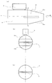
- FIG. 1 is a configuration diagram of a polarization demultiplexer according to Embodiment 1 of the present invention.
- FIG. It is a see-through
- FIG. 1 is a perspective side view, a side view, and a cross-sectional view of a demultiplexer according to a first embodiment of the present invention. It is a see-through
- FIG. 6 is a perspective top view of a polarization separator according to a second embodiment of the present invention. It is the see-through
- FIG. Embodiment 1 of the present invention will be described below with reference to FIGS. 1A is a top view of the demultiplexer
- FIG. 1B is a top view of the demultiplexer (the conductor wall (septum plate) is indicated by a dotted line)
- FIG. 1C is FIG. 2) is a cross-sectional view of the demultiplexer along the one-dot chain line AA
- the two-dot chain line BB in FIG. 1 indicates the boundary between the functions of the circular waveguide and the connection waveguide.
- FIG. 3 (a) is a perspective side view of the demultiplexer (the conductor wall (septum plate) is indicated by a dotted line), and FIG. 3 (b) is the demultiplexer as viewed from the arrow B in FIG. FIG.
- the same reference numerals denote the same or corresponding parts, and detailed descriptions thereof are omitted.
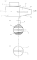
- FIG. 5A is a transparent top view of the demultiplexer (the coupling hole and the rectangular sub-waveguide are omitted), and FIGS. 5B and 5E are dashed-dotted lines AA shown in FIG. 5 (c) and 5 (f) are cross-sectional views of the demultiplexer along the alternate long and short dash line BB described in FIG. 5 (a), and FIGS. 5 (d) and 5 (g) are FIGS.
- FIG. 6A is a cross-sectional view of the demultiplexer along the alternate long and short dash line CC shown in FIG. 6A, and FIG. 6A is a transparent top view of the demultiplexer (the coupling hole and the rectangular sub-waveguide are omitted), FIG.
- FIG. 7 (a) is a perspective side view of the demultiplexer (conductor).
- the wall (septum plate) is indicated by a dotted line
- FIG. (A) a side view of a polarization separator as seen from the arrow B according to FIG. 7 (c) is a sectional view of a polarization separator by dotted AA according in Figure 7 (a).
- the same reference numerals denote the same or corresponding parts, and detailed descriptions thereof are omitted.
- 1 is a circular waveguide (circular main waveguide), 2 is arranged in the axial direction (coaxial direction) in which the circular waveguide 1 extends, and is larger than the inner diameter of the circular waveguide 1.
- a rectangular waveguide having a short side with a short length (rectangular waveguide, rectangular main waveguide, rectangular main waveguide, coaxial side rectangular sub-waveguide), 3 is a rectangular waveguide 2 and a circular waveguide 1 and 4 are formed across the connection waveguide 3 and the circular waveguide 1, and are arranged in parallel to the direction in which the long side of the rectangular waveguide 2 extends.
- the flat conductor wall (septum plate, short-circuit plate) 3a that divides the inside of the circular waveguide 1 and the connection waveguide 3 is connected to the conductor wall (septum plate) 4 at a position facing one surface.
- a first inclined surface 3b is formed on the inner wall of the wave tube 3 and is inclined to the conductor wall 4 side toward the rectangular waveguide 2 side, and is opposed to the other surface of the conductor wall (septum plate) 4. It formed on the inner wall of the connecting waveguide 3 at that position, as toward the rectangular waveguide 2 side, a second inclined surface inclined to the conductor wall 4 side.
- the same reference numerals denote the same or corresponding parts, and detailed descriptions thereof are omitted.
- ⁇ may be a value that does not hinder the connection between the circular waveguide 1 (connection waveguide 3) and the rectangular waveguide 2.
- the circular waveguide 1 is substantially circular, the inner diameter is constant over the circumference, and the length of the long side of the rectangular waveguide 2 is a circular waveguide. It may be substantially the same as the inner diameter of 1 or shorter than the inner diameter of the circular waveguide 1 (in the connection waveguide 3, it corresponds to the inner diameter of the portion other than the first inclined surface 3a and the second inclined surface 3b).
- 5 is formed in the circular waveguide 1.
- This is a coupling hole that branches off the tube 1 and is provided in the radial direction of the circular waveguide 1.
- the coupling hole 5 is formed at a position facing a part of one or the other surface of the conductor wall 4.
- Reference numeral 6 denotes a rectangular sub-waveguide (rectangular sub-waveguide, orthogonal rectangular sub-waveguide) that takes out electromagnetic waves in the orthogonal direction of the circular main waveguide through the coupling hole 5, and 3 c constitutes the connection waveguide 2.
- the arcuate first wall surface 3d constitutes the connecting waveguide 2 and is an arcuate second wall surface facing the first wall surface 3c.
- the first wall surface 3c and the second wall surface 3d are opposed to each other with the center point side of the arc facing each other.
- the connection waveguide 2 includes a first wall surface 3c and a second wall surface 3d having an arc shape facing the first wall surface 3c, a first inclined surface 3a, and a second inclined surface 3b.
- the conductor wall 4 is formed on the first wall surface 3 c and the second wall surface 3 d and divides the inside of the connection waveguide 3.
- the connection waveguide 3 is formed in an H shape by the conductor wall 4, the first wall surface 3c, and the second wall surface 3d. Further, when the first inclined surface 3a and the second inclined surface 3b are also added, the connection waveguide 3 has a shape like a ⁇ character.
- the same reference numerals denote the same or corresponding parts, and detailed descriptions thereof are omitted.
- the circular waveguide 1 and the rectangular shape are given priority to the easy understanding of the structure and positional relationship (particularly, the inner wall structure of the waveguide structure of the demultiplexer according to the first embodiment).
- the conductor thicknesses of the waveguide 2, the connection waveguide 3, and the rectangular sub-waveguide 6 are represented by line segments.
- a circular waveguide 1 is a connection waveguide having a first inclined surface 3a and a second inclined surface 3b having surfaces having a hyperbolic shape obtained by dividing an oblong shape in a coaxial direction. What is connected to the tube 3 is described.
- the first inclined surface 3a and the second inclined surface 3b are surfaces having a linear inclination (taper), but the taper (inclination) is not a linear shape but is a curve defined by a trigonometric function of cosine or sine. It may be a shape.
- the connection waveguide 3 is connected to the rectangular waveguide 2.
- the circular waveguide 1 is provided with a coupling hole 5 in the orthogonal direction, and the coupling hole 5 is connected to the rectangular sub-waveguide 6.
- the conductor wall 4 is disposed in the waveguide (the waveguide structure of the polarization separator according to the first embodiment) from the circular waveguide 1 to the connection waveguide 3. 1 to 3, it can be seen that the coupling hole 5 is formed at a position facing a part of one (other) surface of the conductor wall 4. A part of the conductor wall 4 can be seen from the opening of the rectangular sub-waveguide 6 shown in FIGS. Similarly, the direction in which the long side of the rectangular waveguide 2 extends from the opening of the rectangular waveguide 2 illustrated in FIG. 3B and the direction in which the short side of the rectangular waveguide 2 extends. A conductor plate 4 extending in a direction perpendicular to the line is visible.
- the first wall surface 3c and the second wall surface 3d which are side walls connecting the first inclined surface 3a and the second inclined surface 3b of the connection waveguide 3, are used.
- An explanation will be given.
- the demultiplexer shown in FIG. 4 shows that the inner diameter (a) of the circular waveguide 1 is longer than the length (b) of the long side of the rectangular waveguide 2, and FIG. In the illustrated demultiplexer, the inner diameter (a) of the circular waveguide 1 is shorter than the length (b) of the long side of the rectangular waveguide 2.
- the conductor wall 4 has a rectangular shape on one surface and the other surface.
- the conductor wall 4 is not a flat plate having a stepped outer shape. This is due to the structure and shape of the first wall surface 3c and the second wall surface 3d. 4 and 5 (a) and FIGS. 5 (b) to 5 (d), the connecting waveguide 3 is obtained by cutting the upper and lower sides of the circle (circular waveguide 1) shown in FIG. 5 (b) with parallel lines. It can be seen that the interval between the upper and lower parallel lines is changed while maintaining the same diameter as the circular waveguide 1 (FIGS. 5C and 5D).
- the connecting waveguide 3 has the arc-shaped first wall surface 3c having the same diameter as the inner diameter of the circular waveguide 1 and the first It can be said that it is composed of an arcuate second wall surface 3d facing the wall surface 3c and having the same diameter as the inner diameter of the circular waveguide 1, and the first inclined surface 3a and the second inclined surface 3b. Therefore, the conductor wall 4 is extended over the connecting waveguide 3 and the circular waveguide 1 in such a way that it passes to the center of the opposing arc of the first wall surface 3c and the second wall surface 3d (connects the center of the arc). By forming, the conductor wall 4 can have a rectangular shape instead of a flat plate having a stepped outer shape.
- the first wall surface 3c and the second wall surface 3d are described as having the same shape in the coaxial direction.
- the first wall surface 3c and the second wall surface 3d may not have the same shape in the coaxial direction.
- the conductor wall 4 can be formed into a rectangular shape instead of a flat plate having a stepped outer shape. 4 and 5 (a) and FIGS. 5 (e) to 5 (g).
- the connecting waveguide 3 is connected to the circular waveguide 1, and the arc-shaped first wall surface 3c having the same diameter as the inner diameter of the circular waveguide 1 and the first waveguide 3
- the first wall surface 3c is opposed to the circular waveguide 1 and has an arc-shaped second wall surface 3d having the same diameter as the inner diameter of the circular waveguide 1, a first inclined surface 3a, and a second inclined surface 3b. It is described that the diameters of the arcs of the first wall surface 3c and the second wall surface 3d become larger toward the waveguide 2 side.
- the distance between the centers of the arcs facing each other of the first wall surface 3c and the second wall surface 3d is the same as that of the first wall surface 3c and the second wall surface 3d shown in FIGS. It becomes easy to make it constant.
- the conductor wall 4 has been described as having a rectangular shape, but in the connection portion between the circular waveguide 1 and the connection waveguide 3 where the conductor wall 4 is formed, If a large step does not occur, the demultiplexer according to Embodiment 1 can be implemented. That is, it can be said that the case where the long side of the rectangular waveguide 2 is shorter than the inner diameter of the circular waveguide 1 is also included in the demultiplexer according to the first embodiment. This case will be described with reference to FIG. 6, the conductor wall 4 has a rectangular shape on one surface and the other surface of the circular waveguide 1, and the one surface and the other surface of the connection waveguide 3. The surface has a trapezoidal shape.
- FIGS. 6 (a) to 6 (g) correspond to FIGS. 5 (a) to 5 (g), respectively.
- the demultiplexer shown in FIG. 6 shows that the inner diameter (a) of the circular waveguide 1 is longer than the length (b) of the long side of the rectangular waveguide 2.
- the connecting waveguide 3 is an oval type obtained by cutting the upper and lower sides of the circle (circular waveguide 1) shown in FIG. 6B with parallel lines.
- the first wall surface 3c and the second wall surface 3d have the same diameter as the circular waveguide 1 and the interval between the upper and lower parallel lines is changed. It can be seen that they are approaching (FIGS. 6C and 6D).
- the connecting waveguide 3 is connected to the circular waveguide 1 at the arc-shaped first wall surface 3c and the first wall surface 3c, and the arc-shaped second wall surface 4d, the first inclined surface 3a and the first inclined surface 3a. 2, and the distance between the first wall surface 3c and the second wall surface 3d becomes narrower from the circular waveguide 1 side toward the rectangular waveguide 2 side (FIG. 6C). d))
- the conductor wall 4 is in the connection waveguide 3, and one surface and the other surface are trapezoidal.
- the connecting waveguide 3 is in the shape of an arc having the same diameter as the inner diameter of the circular waveguide 1 at the portion connected to the circular waveguide 1.
- the first wall surface 3c and the first wall surface 3c of the circular waveguide 1 are opposed to each other and formed of an arc-shaped second wall surface 3d having the same diameter as the inner diameter of the circular waveguide 1, a first inclined surface 3a, and a second inclined surface 3b. It can be said that the distance between the first wall surface 3c and the second wall surface 3d becomes narrower from the waveguide 1 side toward the rectangular waveguide 2 side.
- the conductor wall 4 is extended over the connecting waveguide 3 and the circular waveguide 1 in such a way that it passes to the center of the opposing arc of the first wall surface 3c and the second wall surface 3d (connects the center of the arc).
- the conductor wall 4 can have a shape that combines a rectangular shape and a trapezoidal shape instead of a flat plate having a stepped outer shape.
- the arcuate first wall surface having the same diameter as the inner diameter of the circular waveguide 1 in the portion where the connecting waveguide 3 is connected to the circular waveguide 1.
- the circular waveguide 1 is composed of an arc-shaped second wall surface 3d facing the 3c and the first wall surface 3c and having the same diameter as the inner diameter of the circular waveguide 1, and a first inclined surface 3a and a second inclined surface 3b.
- the distance between the first wall surface 3c and the second wall surface 3d is preferably increased from the side toward the rectangular waveguide 2 side.
- the diameter in contact with or near the rectangular waveguide 2 is larger than the length of the long side of the rectangular waveguide 2.
- the difference needs to be in the range of ⁇ described above.
- FIGS. 6B to 6D show that the first wall surface 3c and the second wall surface 3d have the same shape in the coaxial direction, but they may not have the same shape in the coaxial direction.
- the conductor wall 4 is not a flat plate having a stepped outer shape but a shape combining a rectangular shape and a trapezoidal shape. The case where this can be achieved will be described with reference to FIG. 6A and FIGS. 6E to 6G.
- first wall surface 3c having the same diameter as the inner diameter of the circular waveguide 1 and the first
- the first wall surface 3c is opposed to the circular waveguide 1 and has an arc-shaped second wall surface 3d having the same diameter as the inner diameter of the circular waveguide 1, a first inclined surface 3a, and a second inclined surface 3b. It is described that the distance between the first wall surface 3c and the second wall surface 3d becomes narrower and the diameters of the arcs of the first wall surface 3c and the second wall surface 3d become larger toward the waveguide 2 side. .
- the reduction ratio in the distance between the centers of the arcs facing each other of the first wall surface 3c and the second wall surface 3d is the first wall surface 3c and the second wall surface 3d described in FIGS. 6 (b) to 6 (d). It is easy to do the same.
- the arcuate first wall surface having the same diameter as the inner diameter of the circular waveguide 1 in the portion where the connecting waveguide 3 is connected to the circular waveguide 1.
- the circular waveguide 1 is composed of an arc-shaped second wall surface 3d facing the 3c and the first wall surface 3c and having the same diameter as the inner diameter of the circular waveguide 1, and a first inclined surface 3a and a second inclined surface 3b.
- the distance between the first wall surface 3c and the second wall surface 3d increases, and the arc diameters of the first wall surface 3c and the second wall surface 3d increase.
- the diameter in contact with or near the rectangular waveguide 2 is larger than the length of the long side of the rectangular waveguide 2. Although it may be long or short, the difference needs to be in the range of ⁇ described above.
- the demultiplexer according to the first embodiment includes a circular main waveguide 1 capable of transmitting orthogonally polarized waves, a rectangular sub-waveguide 6 connected in a radial direction via a coupling hole 5, and a circular main waveguide. 1 and a rectangular waveguide 2 connected through a connecting waveguide 3 in the coaxial direction.
- the connecting waveguide 3 has an oval cross section obtained by cutting the upper and lower sides of the circular waveguide 3 with parallel straight lines, and the upper and lower heights change into a tapered shape.
- a conductor wall (septum plate) 4 disposed in the straddled region is provided.
- the circular waveguide 1 transmits orthogonally polarized waves, and transmits radio waves (electromagnetic waves) to the rectangular waveguide 2 via the connection waveguide 3 or to the rectangular sub-waveguide 6 via the coupling hole 5.
- the radio wave from the rectangular waveguide 2 is output to the end of the circular waveguide 1.
- a radio wave from the rectangular sub-waveguide 6 is output to the end of the circular waveguide 1.
- the connecting waveguide 3 performs matching between the circular waveguide 1 and the rectangular waveguide 2.
- the connection waveguide 3 is formed in the above-described oval shape, so that it can be guided in a range where the outer shape is circular. Since the width (or diameter) of the wave tube does not change, a thin plate-like septum plate (conductor wall) 4 can be easily disposed or processed across the circular waveguide 1 and the connection waveguide 3. Further, since the change in the width (or diameter) of the waveguide is small in the range where the outer shape is circular, a thin plate-like septum plate (conductor wall) straddling the circular waveguide 1 and the connection waveguide 3. 4 can be easily arranged or processed.
- FIG. A second embodiment of the present invention will be described with reference to FIGS. 9A is a perspective side view of the demultiplexer (the conductor wall (septum plate) is indicated by a dotted line), and FIG. 9B is the demultiplexer viewed from the arrow B in FIG. 9A.
- 11A is a transparent top view of the demultiplexer (with the coupling hole and the rectangular sub-waveguide omitted)
- FIG. 11B is a transparent top view of the demultiplexer
- FIG. 12 (a) is a perspective side view of the polarization demultiplexer (the conductor wall (septum plate) is indicated by a dotted line)
- FIG. 12 (b) is FIG.
- FIG. 12 (a) is a perspective side view of the polarization demultiplexer (the conductor wall (septum plate) is indicated by a dotted line)
- FIG. 12 (b) is FIG.
- FIG. 12 (a) is a perspective side view of the polarization
- FIG. 12C is a side view of the demultiplexer viewed from the arrow B in FIG. 12A, and FIG. 12C is a cross-sectional view of the demultiplexer along the dotted line AA in FIG.
- the same reference numerals denote the same or corresponding parts, and detailed descriptions thereof are omitted.
- the polarization demultiplexer according to the second embodiment will be described with reference to FIGS.
- the points (first inclined surface 3a and second inclined surface 3b) different from the first embodiment will be described, but the description of the common parts will be omitted.
- the demultiplexer according to the second embodiment is the same as the demultiplexer according to the first embodiment, but has a linear inclination (taper), or a curved inclination defined by a trigonometric function of cosine or sine.
- the difference is that the first inclined surface 3a and the second inclined surface 3b, which are surfaces, have a stepped shape.
- the stepwise inclination of the first inclined surface 3a and the second inclined surface 3b simulates the inclined surfaces of the first inclined surface 3a and the second inclined surface 3b in the first embodiment. That is, when one step of the staircase portion by the first inclined surface 3a and the second inclined surface 3b is connected by a straight line or a curve, the approximate shape approximates the first inclined surface 3a and the second inclined surface 3b in the first embodiment. It will be a thing.
- FIGS. 8 to 10 correspond to FIGS. 2 to 4 used for explaining the demultiplexer according to the first embodiment, respectively.
- the circular waveguide 1 includes a first inclined surface 3a and a second inclined surface 3a having pyramid-shaped steps on a hyperbolic portion of a surface having a hyperbolic shape obtained by dividing an oval shape in the coaxial direction. What is connected to the connecting waveguide 3 having the inclined surface 3b is described.
- the first inclined surface 3a and the second inclined surface 3b have a stepped shape simulating a surface having a linear inclination (taper) or a curved shape defined by a trigonometric function of cosine or sine. Processing is easy.
- the staircase shape may simulate a curved shape defined by a linear slope, a trigonometric function, or the like, or may be a staircase shape formed by an impedance matching device such as a quarter wavelength matching device. It doesn't matter. Needless to say, the 1 ⁇ 4 wavelength refers to the frequency (wavelength) of the demultiplexer (waveguide) used.
- both the conductor wall 4 having a rectangular shape and the conductor wall 4 having a rectangular shape and a trapezoidal shape are used. It can be seen that it is acceptable.
- the demultiplexer according to the second embodiment includes the circular main waveguide 1 capable of transmitting orthogonal polarized waves, the rectangular sub-waveguide 6 connected in the radial direction via the coupling hole, and the circular waveguide.
- the configuration of the tube 1 and the rectangular waveguide 2 connected in the axial direction via the connecting waveguide 3 is the same as that of the demultiplexer according to the first embodiment. Absent.
- the difference between the second embodiment and the first embodiment is that the demultiplexer according to the second embodiment has an oval cross section in which the upper and lower sides of the connection waveguide 3 are cut by parallel straight lines. Is changed in a step shape (step shape).
- the circular waveguide 1 and the connection waveguide 3 are preferably integrally formed by a general processing method such as cutting or die casting.
- the conductor wall 4 is also preferably formed integrally with the circular waveguide 1 and the connection waveguide 3 by a general processing method such as cutting or die casting.
- the connection waveguide 3 and the rectangular waveguide 2 may be connected using a general waveguide connection method.
- connection waveguide 3 When the circular waveguide 1 and the connection waveguide 3 are integrated, in the first embodiment, the end portion of the circular waveguide 1 on the side connected to the rectangular waveguide 2 is used.
- the conductor wall (septum plate) 4 is arranged in a region extending between the circular waveguide 1 and the taper conversion portion of the circular waveguide 1.
- the connection waveguide 3 can be understood as a step conversion unit provided at the end of the circular waveguide 1 on the side connected to the rectangular waveguide 2, and a conductor wall (septum) The plate 4 is arranged in a region extending between the circular waveguide 1 and the step converter of the circular waveguide 1.
- the circular waveguide 1 is substantially circular, the inner diameter is constant over the circumference, and the length of the long side of the rectangular waveguide 2 is the circular waveguide 1. That is substantially the same as the inner diameter of the waveguide (the difference in diameter within the range of ⁇ described above), or that the length of the long side of the rectangular waveguide 2 is shorter than the inner diameter of the circular waveguide 1 (a diameter that exceeds ⁇ described above)
- the circular waveguide 1 is elliptical, the longer side of the rectangular waveguide 2 is aligned with the longer one of the inner diameters, and the longer side of the rectangular waveguide 2 is aligned with the shorter one.
- the demultiplexer according to the first and second embodiments can be applied.
- the structure of the conductor wall (septum plate) 4 of the demultiplexer in the invention according to the present application can be reproduced, the demultiplexer according to the first and second embodiments can be applied. Therefore, it is clear that there is no departure from the spirit of the invention according to the present application.
- the demultiplexer according to the present application is a circular waveguide 1 and a connection (connected or integral) connected to one opening of the circular waveguide 1.
- the waveguide 3 (when integrated with the circular waveguide 1, as described above, it becomes a taper conversion part of the circular waveguide 1 or a step conversion part of the circular waveguide 1), and the connection waveguide 3 And the flat waveguide wall 4 that divides the inside of the circular waveguide 1 and the connection waveguide 3, and a position facing one surface of the conductor wall 4.
- connection waveguide 3 on the side that can be connected to the rectangular waveguide 2 is an ellipse or a square, and the corner portions (four corners) are arcuate.
- the conductor wall 4 is arrange
- the taper converter of the circular waveguide 1 or the step converter of the circular waveguide 1 is formed on the side of the rectangular waveguide 2 that can be connected to the circular waveguide 1 in the circular waveguide 1.
- a demultiplexer is arranged in the axial direction of a circular waveguide and connects a rectangular waveguide having a short side shorter than the inner diameter of the circular waveguide and the circular waveguide.
- a coupling hole for extracting one of the electromagnetic waves propagating in the waveguide and propagating through the circular waveguide and depolarized by the conductor wall Equipped with a conductor wall (septum plate) is easy to manufacture, and the range in which the length of the septum plate can be adjusted increases to improve the electrical performance such as broadening the band. Suitable for use in containers.
- 1 circular waveguide (circular main waveguide), 2 rectangular waveguide (rectangular waveguide, rectangular main waveguide, rectangular main waveguide, coaxial side rectangular waveguide), 3 connecting waveguide, 3a 1st inclined surface, 3b 2nd inclined surface, 3c 1st wall surface, 3d 2nd wall surface, 4 conductor wall (septum plate, short-circuit plate), 5 coupling hole, 6 rectangular sub-waveguide (rectangular sub-waveguide, orthogonal) Side rectangular sub-waveguide).
Landscapes
- Waveguide Switches, Polarizers, And Phase Shifters (AREA)
- Control Of Motors That Do Not Use Commutators (AREA)
- Waveguide Connection Structure (AREA)
- Waveguides (AREA)
- Optical Integrated Circuits (AREA)
Abstract
Description
実施の形態1.
以下、この発明の実施の形態1について図1~7を用いて説明する。図1(a)は偏分波器の上面図、図1(b)は偏分波器の上面図(導体壁(セプタム板)を点線で表示)、図1(c)は図1(a)に記載の一点鎖線AAによる偏分波器の断面図であり、図1における二点鎖線BBは円形導波管と接続導波管との機能の境目を示している。図3(a)は偏分波器に透視側面図(導体壁(セプタム板)を点線で表示)、図3(b)は図3(a)に記載の矢印Bから見た偏分波器の側方図である。図中、同一符号は、同一又は相当部分を示しそれらについての詳細な説明は省略する。
この発明の実施の形態2について図8~12を用いて説明する。図9(a)は偏分波器に透視側面図(導体壁(セプタム板)を点線で表示)、図9(b)は図9(a)に記載の矢印Bから見た偏分波器の側方図、図11(a)は偏分波器の透視上面図(結合孔及び方形副導波管を省略している)、図11(b)は偏分波器の透視上面図(結合孔及び方形副導波管を省略している)、図12(a)は偏分波器の透視側面図(導体壁(セプタム板)を点線で表示)、図12(b)は図12(a)に記載の矢印Bから見た偏分波器の側方図、図12(c)は図12(a)に記載の点線AAによる偏分波器の断面図である。図中、同一符号は、同一又は相当部分を示しそれらについての詳細な説明は省略する。
実施の形態1及び2に係る偏分波器において、円形導波管1及び接続導波管3は、切削加工やダイキャスト鋳造などの一般的な加工方法で一体成形することが好適である。導体壁4も、円形導波管1及び接続導波管3と共に、切削加工やダイキャスト鋳造などの一般的な加工方法で一体成形することが好適である。また、接続導波管3と方形導波管2との接続は、一般的な導波管接続手法を用いればよい。
Claims (27)
- 円形導波管と、この円形導波管の軸方向に配置され、前記円形導波管の内径よりも短い長さの短辺を有する方形導波管と、この方形導波管と前記円形導波管とを接続する接続導波管と、この接続導波管と前記円形導波管とに亘って形成され、前記方形導波管の長辺が延在する方向に対して平行に配置された前記円形導波管及び前記接続導波管の内部を分割する平板状の導体壁と、この導体壁の一方の面に対向する位置における前記接続導波管の内壁に形成され、前記方形導波管側に向かうにつれ、前記導体壁側に傾斜した第1傾斜面と、前記導体壁の他方の面に対向する位置における前記接続導波管の内壁に形成され、前記方形導波管側に向かうにつれ、前記導体壁側に傾斜した第2傾斜面と、前記円形導波管に形成され、前記円形導波管が伝播する電磁波のうち、前記導体壁により偏分波された一方を取り出す結合孔とを備えた偏分波器。
- 前記第1傾斜面及び前記第2傾斜面は、階段状の形状を有するものである請求項1に記載の偏分波器。
- 前記結合孔は、前記導体壁の一方又は他方の面の一部と対向する位置に形成されるものである請求項1に記載の偏分波器。
- 前記導体壁は、前記一方の面及び前記他方の面が長方形状の形状を有するものである請求項1に記載の偏分波器。
- 前記接続導波管は、円弧状の第1壁面及びこの第1壁面と対向する円弧状の第2壁面と前記第1傾斜面及び前記第2傾斜面とから構成されるものである請求項1に記載の偏分波器。
- 前記接続導波管は、前記円形導波管の内径と同じ径の円弧状の第1壁面及びこの第1壁面と対向し、前記円形導波管の内径と同じ径の円弧状の第2壁面と前記第1傾斜面及び前記第2傾斜面とから構成されるものである請求項1に記載の偏分波器。
- 前記接続導波管は、前記円形導波管と接続する部分では、前記円形導波管の内径と同じ径の円弧状の第1壁面及びこの第1壁面と対向し、前記円形導波管の内径と同じ径の円弧状の第2壁面と前記第1傾斜面及び前記第2傾斜面とから構成され、前記円形導波管側から前記方形導波管側に向かうにつれ、前記第1壁面及び前記第2壁面の径が大きくなっていくものである請求項1に記載の偏分波器。
- 前記方形導波管は、その長辺が前記円形導波管の内径よりも短いものである請求項1に記載の偏分波器。
- 前記導体壁は、前記接続導波管における前記一方の面及び前記他方の面が台形状の形状を有するものである請求項1に記載の偏分波器。
- 前記接続導波管は、前記円形導波管と接続する部分では、円弧状の第1壁面及びこの第1壁面と対向する円弧状の第2壁面と前記第1傾斜面及び前記第2傾斜面とから構成され、前記円形導波管側から前記方形導波管側に向かうにつれ、前記第1壁面及び前記第2壁面の距離が狭まっていくものである請求項8に記載の偏分波器。
- 前記接続導波管は、前記円形導波管と接続する部分では、円弧状の第1壁面及びこの第1壁面と対向する円弧状の第2壁面と前記第1傾斜面及び前記第2傾斜面とから構成され、前記円形導波管側から前記方形導波管側に向かうにつれ、前記第1壁面及び前記第2壁面の距離が狭まっていくものである請求項9に記載の偏分波器。
- 前記接続導波管は、前記円形導波管と接続する部分では、前記円形導波管の内径と同じ径の円弧状の第1壁面及びこの第1壁面と対向し、前記円形導波管の内径と同じ径の円弧状の第2壁面と前記第1傾斜面及び前記第2傾斜面とから構成され、前記円形導波管側から前記方形導波管側に向かうにつれ、前記第1壁面及び前記第2壁面の距離が狭まっていくものである請求項8に記載の偏分波器。
- 前記接続導波管は、前記円形導波管と接続する部分では、前記円形導波管の内径と同じ径の円弧状の第1壁面及びこの第1壁面と対向し、前記円形導波管の内径と同じ径の円弧状の第2壁面と前記第1傾斜面及び前記第2傾斜面とから構成され、前記円形導波管側から前記方形導波管側に向かうにつれ、前記第1壁面及び前記第2壁面の距離が狭まっていくものである請求項9に記載の偏分波器。
- 前記接続導波管は、前記円形導波管と接続する部分では、前記円形導波管の内径と同じ径の円弧状の第1壁面及びこの第1壁面と対向し、前記円形導波管の内径と同じ径の円弧状の第2壁面と前記第1傾斜面及び前記第2傾斜面とから構成され、前記円形導波管側から前記方形導波管側に向かうにつれ、前記第1壁面及び前記第2壁面の距離が狭まっていくと共に、前記第1壁面及び前記第2壁面の径が大きくなっていくものである請求項8に記載の偏分波器。
- 前記接続導波管は、前記円形導波管と接続する部分では、前記円形導波管の内径と同じ径の円弧状の第1壁面及びこの第1壁面と対向し、前記円形導波管の内径と同じ径の円弧状の第2壁面と前記第1傾斜面及び前記第2傾斜面とから構成され、前記円形導波管側から前記方形導波管側に向かうにつれ、前記第1壁面及び前記第2壁面の距離が狭まっていくと共に、前記第1壁面及び前記第2壁面の径が大きくなっていくものである請求項9に記載の偏分波器。
- 前記導体壁は、前記第1壁面と前記第2壁面とに形成され、前記接続導波管の内部を分割するものである請求項5に記載の偏分波器。
- 前記導体壁は、前記第1壁面と前記第2壁面とに形成され、前記接続導波管の内部を分割するものである請求項6に記載の偏分波器。
- 前記導体壁は、前記第1壁面と前記第2壁面とに形成され、前記接続導波管の内部を分割するものである請求項7に記載の偏分波器。
- 前記導体壁は、前記第1壁面と前記第2壁面とに形成され、前記接続導波管の内部を分割するものである請求項10に記載の偏分波器。
- 前記導体壁は、前記第1壁面と前記第2壁面とに形成され、前記接続導波管の内部を分割するものである請求項11に記載の偏分波器。
- 前記導体壁は、前記第1壁面と前記第2壁面とに形成され、前記接続導波管の内部を分割するものである請求項12に記載の偏分波器。
- 前記導体壁は、前記第1壁面と前記第2壁面とに形成され、前記接続導波管の内部を分割するものである請求項13に記載の偏分波器。
- 前記導体壁は、前記第1壁面と前記第2壁面とに形成され、前記接続導波管の内部を分割するものである請求項14に記載の偏分波器。
- 前記導体壁は、前記第1壁面と前記第2壁面とに形成され、前記接続導波管の内部を分割するものである請求項15に記載の偏分波器。
- 前記円形導波管と前記接続導波管とは、一体である請求項1に記載の偏分波器。
- 前記導体壁は、前記円形導波管及び前記方形導波管と一体である請求項25に記載の偏分波器。
- 円形導波管と、この円形導波管の一方の開口と連通する接続導波管と、この接続導波管と前記円形導波管とに亘って形成され、前記円形導波管及び前記接続導波管の内部を分割する平板状の導体壁と、この導体壁の一方の面に対向する位置における前記接続導波管の内壁に形成され、前記円形導波管と反対側に向かうにつれ、前記導体壁側に傾斜した第1傾斜面と、前記導体壁の他方の面に対向する位置における前記接続導波管の内壁に形成され、前記円形導波管と反対側に向かうにつれ、前記導体壁側に傾斜した第2傾斜面と、前記円形導波管に形成され、前記円形導波管が伝播する電磁波のうち、前記導体壁により偏分波された一方を取り出す結合孔とを備えたことを特徴とする偏分波器。
Priority Applications (4)
| Application Number | Priority Date | Filing Date | Title |
|---|---|---|---|
| KR1020147012892A KR101596236B1 (ko) | 2011-11-17 | 2012-11-16 | 편분파기 |
| CN201280056547.2A CN103999284B (zh) | 2011-11-17 | 2012-11-16 | 偏振分波器 |
| US14/238,658 US9000861B2 (en) | 2011-11-17 | 2012-11-16 | Polarization coupler |
| EP12849068.7A EP2782186A4 (en) | 2011-11-17 | 2012-11-16 | POLARIZATION COUPLER |
Applications Claiming Priority (2)
| Application Number | Priority Date | Filing Date | Title |
|---|---|---|---|
| JP2011-251663 | 2011-11-17 | ||
| JP2011251663A JP5477362B2 (ja) | 2011-11-17 | 2011-11-17 | 偏分波器 |
Publications (1)
| Publication Number | Publication Date |
|---|---|
| WO2013073674A1 true WO2013073674A1 (ja) | 2013-05-23 |
Family
ID=48429727
Family Applications (1)
| Application Number | Title | Priority Date | Filing Date |
|---|---|---|---|
| PCT/JP2012/079807 WO2013073674A1 (ja) | 2011-11-17 | 2012-11-16 | 偏分波器 |
Country Status (6)
| Country | Link |
|---|---|
| US (1) | US9000861B2 (ja) |
| EP (1) | EP2782186A4 (ja) |
| JP (1) | JP5477362B2 (ja) |
| KR (1) | KR101596236B1 (ja) |
| CN (1) | CN103999284B (ja) |
| WO (1) | WO2013073674A1 (ja) |
Families Citing this family (10)
| Publication number | Priority date | Publication date | Assignee | Title |
|---|---|---|---|---|
| JP5800689B2 (ja) * | 2011-11-17 | 2015-10-28 | 三菱電機株式会社 | 偏分波器 |
| KR101514155B1 (ko) * | 2013-12-24 | 2015-04-21 | 단국대학교 천안캠퍼스 산학협력단 | 도파관 다이플렉서 |
| US9859597B2 (en) | 2015-05-27 | 2018-01-02 | Viasat, Inc. | Partial dielectric loaded septum polarizer |
| US9640847B2 (en) | 2015-05-27 | 2017-05-02 | Viasat, Inc. | Partial dielectric loaded septum polarizer |
| US10020554B2 (en) | 2015-08-14 | 2018-07-10 | Viasat, Inc. | Waveguide device with septum features |
| US10096876B2 (en) | 2015-11-13 | 2018-10-09 | Viasat, Inc. | Waveguide device with sidewall features |
| CN107952582A (zh) * | 2017-03-20 | 2018-04-24 | 陈萍 | 一种石墨多级阶梯状除铁器 |
| RU2691673C1 (ru) * | 2018-06-29 | 2019-06-17 | Публичное акционерное общество "Радиофизика" | Волноводный поляризационный селектор |
| CN112510337B (zh) * | 2020-11-27 | 2022-02-01 | 江苏亨通太赫兹技术有限公司 | 基于模式合成的交叉耦合器及构建方法、阻抗匹配结构 |
| JP7305079B2 (ja) * | 2021-03-25 | 2023-07-07 | 三菱電機株式会社 | 偏分波器 |
Citations (6)
| Publication number | Priority date | Publication date | Assignee | Title |
|---|---|---|---|---|
| JPS5690601A (en) * | 1979-12-24 | 1981-07-22 | Fujitsu Ltd | Polarization coupler |
| JPH01273401A (ja) | 1988-04-26 | 1989-11-01 | Nec Corp | 分波器 |
| JPH06140810A (ja) | 1992-10-22 | 1994-05-20 | Nec Corp | 直交偏分波器 |
| JPH0794905A (ja) * | 1993-04-22 | 1995-04-07 | Hughes Aircraft Co | サイドポート窓を有する直交モード変換器 |
| JPH08162804A (ja) | 1994-12-09 | 1996-06-21 | Nec Eng Ltd | 直交偏分波器 |
| JPH09186506A (ja) * | 1995-10-31 | 1997-07-15 | Nec Eng Ltd | 分波器 |
Family Cites Families (10)
| Publication number | Priority date | Publication date | Assignee | Title |
|---|---|---|---|---|
| GB818447A (en) * | 1956-10-31 | 1959-08-19 | Bendix Aviat Corp | Microwave antenna feed for circular polarization |
| JPS6427301A (en) * | 1987-07-23 | 1989-01-30 | Matsushita Electric Ind Co Ltd | High frequency polarizer |
| JPH01138801A (ja) * | 1987-11-26 | 1989-05-31 | Toshiba Corp | 偏分波器 |
| JPH03253101A (ja) | 1990-03-02 | 1991-11-12 | Nippon Hoso Kyokai <Nhk> | 偏分波器 |
| JPH0722803A (ja) * | 1993-06-30 | 1995-01-24 | Mitsubishi Electric Corp | 偏分波器 |
| JPH0758502A (ja) * | 1993-08-19 | 1995-03-03 | Nec Eng Ltd | 分波器 |
| KR0167048B1 (en) * | 1993-10-29 | 1999-03-30 | Dai Ichi Kogyo Seiyaku Co Ltd | Thermoplastic resin composition |
| JP3341101B2 (ja) * | 1995-07-28 | 2002-11-05 | 日本電気エンジニアリング株式会社 | アンテナ気密構造 |
| FR2740614B1 (fr) * | 1995-10-31 | 1998-04-24 | Nec Corp | Filtre de separation de micro-ondes |
| CN201327867Y (zh) * | 2008-12-03 | 2009-10-14 | 中国航天科技集团公司第五研究院第五〇四研究所 | 一种宽带正交模耦合器 |
-
2011
- 2011-11-17 JP JP2011251663A patent/JP5477362B2/ja active Active
-
2012
- 2012-11-16 EP EP12849068.7A patent/EP2782186A4/en not_active Withdrawn
- 2012-11-16 US US14/238,658 patent/US9000861B2/en not_active Expired - Fee Related
- 2012-11-16 CN CN201280056547.2A patent/CN103999284B/zh not_active Expired - Fee Related
- 2012-11-16 WO PCT/JP2012/079807 patent/WO2013073674A1/ja active Application Filing
- 2012-11-16 KR KR1020147012892A patent/KR101596236B1/ko active IP Right Grant
Patent Citations (6)
| Publication number | Priority date | Publication date | Assignee | Title |
|---|---|---|---|---|
| JPS5690601A (en) * | 1979-12-24 | 1981-07-22 | Fujitsu Ltd | Polarization coupler |
| JPH01273401A (ja) | 1988-04-26 | 1989-11-01 | Nec Corp | 分波器 |
| JPH06140810A (ja) | 1992-10-22 | 1994-05-20 | Nec Corp | 直交偏分波器 |
| JPH0794905A (ja) * | 1993-04-22 | 1995-04-07 | Hughes Aircraft Co | サイドポート窓を有する直交モード変換器 |
| JPH08162804A (ja) | 1994-12-09 | 1996-06-21 | Nec Eng Ltd | 直交偏分波器 |
| JPH09186506A (ja) * | 1995-10-31 | 1997-07-15 | Nec Eng Ltd | 分波器 |
Non-Patent Citations (1)
| Title |
|---|
| See also references of EP2782186A4 |
Also Published As
| Publication number | Publication date |
|---|---|
| EP2782186A1 (en) | 2014-09-24 |
| US9000861B2 (en) | 2015-04-07 |
| EP2782186A4 (en) | 2015-06-24 |
| JP2013110456A (ja) | 2013-06-06 |
| KR20140072916A (ko) | 2014-06-13 |
| CN103999284B (zh) | 2016-07-06 |
| US20140197908A1 (en) | 2014-07-17 |
| KR101596236B1 (ko) | 2016-02-22 |
| CN103999284A (zh) | 2014-08-20 |
| JP5477362B2 (ja) | 2014-04-23 |
Similar Documents
| Publication | Publication Date | Title |
|---|---|---|
| WO2013073674A1 (ja) | 偏分波器 | |
| US11031692B1 (en) | System including antenna and ultra-wideband ortho-mode transducer with ridge | |
| US9673532B2 (en) | Antenna | |
| US8354969B2 (en) | Polarizer and waveguide antenna apparatus using the same | |
| JP5566169B2 (ja) | アンテナ装置 | |
| JP2004363764A (ja) | 導波管装置 | |
| KR100579209B1 (ko) | 전송 선로 트랜지션 | |
| JP2010192987A (ja) | 同軸コネクタ、同軸コネクタ・平面線路接続構造 | |
| JP4753981B2 (ja) | 導波管・ストリップ線路変換器 | |
| WO2015182243A1 (ja) | 円偏波発生器 | |
| JP2010028345A (ja) | 導波管・ストリップ線路変換器及び高周波回路 | |
| JP2018117173A (ja) | 90度ハイブリッド回路 | |
| US11101530B2 (en) | Polarization separation circuit | |
| JP6490358B2 (ja) | 同軸偏光子での使用のための対向する浅いキャビティを備えた内側チューブ | |
| US6624715B2 (en) | Ultrawide-band linear-circular polarization converter | |
| WO2024047776A1 (ja) | 偏波分離回路およびアンテナ | |
| US10871511B1 (en) | Ultra-wideband ortho-mode transducer with ridge | |
| US9368855B2 (en) | Planar circuit to waveguide transition having openings formed in a conductive pattern to form a balance line or an unbalance line | |
| JP7305079B2 (ja) | 偏分波器 | |
| WO2023206814A1 (zh) | 正交模耦合器和双线极化馈源 | |
| US20230223701A1 (en) | Antenna device | |
| JP2006005818A (ja) | マイクロ波受信用コンバータ | |
| JP2008004360A (ja) | 先端短絡(λ/4)同軸回路 | |
| KR101839888B1 (ko) | 폭이 넓은 회로의 패키징을 위한 도파관 변환 장치 | |
| JP5770508B2 (ja) | 導波管変換器 |
Legal Events
| Date | Code | Title | Description |
|---|---|---|---|
| 121 | Ep: the epo has been informed by wipo that ep was designated in this application |
Ref document number: 12849068 Country of ref document: EP Kind code of ref document: A1 |
|
| WWE | Wipo information: entry into national phase |
Ref document number: 14238658 Country of ref document: US |
|
| ENP | Entry into the national phase |
Ref document number: 20147012892 Country of ref document: KR Kind code of ref document: A |
|
| WWE | Wipo information: entry into national phase |
Ref document number: 2012849068 Country of ref document: EP |
|
| NENP | Non-entry into the national phase |
Ref country code: DE |