WO2013061556A1 - 液晶表示パネル及びその製造方法 - Google Patents
液晶表示パネル及びその製造方法 Download PDFInfo
- Publication number
- WO2013061556A1 WO2013061556A1 PCT/JP2012/006723 JP2012006723W WO2013061556A1 WO 2013061556 A1 WO2013061556 A1 WO 2013061556A1 JP 2012006723 W JP2012006723 W JP 2012006723W WO 2013061556 A1 WO2013061556 A1 WO 2013061556A1
- Authority
- WO
- WIPO (PCT)
- Prior art keywords
- thin film
- pixel
- film transistor
- source
- electrode
- Prior art date
- Legal status (The legal status is an assumption and is not a legal conclusion. Google has not performed a legal analysis and makes no representation as to the accuracy of the status listed.)
- Ceased
Links
Images


Classifications
-
- G—PHYSICS
- G02—OPTICS
- G02F—OPTICAL DEVICES OR ARRANGEMENTS FOR THE CONTROL OF LIGHT BY MODIFICATION OF THE OPTICAL PROPERTIES OF THE MEDIA OF THE ELEMENTS INVOLVED THEREIN; NON-LINEAR OPTICS; FREQUENCY-CHANGING OF LIGHT; OPTICAL LOGIC ELEMENTS; OPTICAL ANALOGUE/DIGITAL CONVERTERS
- G02F1/00—Devices or arrangements for the control of the intensity, colour, phase, polarisation or direction of light arriving from an independent light source, e.g. switching, gating or modulating; Non-linear optics
- G02F1/01—Devices or arrangements for the control of the intensity, colour, phase, polarisation or direction of light arriving from an independent light source, e.g. switching, gating or modulating; Non-linear optics for the control of the intensity, phase, polarisation or colour
- G02F1/13—Devices or arrangements for the control of the intensity, colour, phase, polarisation or direction of light arriving from an independent light source, e.g. switching, gating or modulating; Non-linear optics for the control of the intensity, phase, polarisation or colour based on liquid crystals, e.g. single liquid crystal display cells
- G02F1/133—Constructional arrangements; Operation of liquid crystal cells; Circuit arrangements
- G02F1/136—Liquid crystal cells structurally associated with a semi-conducting layer or substrate, e.g. cells forming part of an integrated circuit
- G02F1/1362—Active matrix addressed cells
- G02F1/136286—Wiring, e.g. gate line, drain line
-
- G—PHYSICS
- G02—OPTICS
- G02F—OPTICAL DEVICES OR ARRANGEMENTS FOR THE CONTROL OF LIGHT BY MODIFICATION OF THE OPTICAL PROPERTIES OF THE MEDIA OF THE ELEMENTS INVOLVED THEREIN; NON-LINEAR OPTICS; FREQUENCY-CHANGING OF LIGHT; OPTICAL LOGIC ELEMENTS; OPTICAL ANALOGUE/DIGITAL CONVERTERS
- G02F1/00—Devices or arrangements for the control of the intensity, colour, phase, polarisation or direction of light arriving from an independent light source, e.g. switching, gating or modulating; Non-linear optics
- G02F1/01—Devices or arrangements for the control of the intensity, colour, phase, polarisation or direction of light arriving from an independent light source, e.g. switching, gating or modulating; Non-linear optics for the control of the intensity, phase, polarisation or colour
- G02F1/13—Devices or arrangements for the control of the intensity, colour, phase, polarisation or direction of light arriving from an independent light source, e.g. switching, gating or modulating; Non-linear optics for the control of the intensity, phase, polarisation or colour based on liquid crystals, e.g. single liquid crystal display cells
- G02F1/133—Constructional arrangements; Operation of liquid crystal cells; Circuit arrangements
- G02F1/136—Liquid crystal cells structurally associated with a semi-conducting layer or substrate, e.g. cells forming part of an integrated circuit
- G02F1/1362—Active matrix addressed cells
- G02F1/13624—Active matrix addressed cells having more than one switching element per pixel
-
- H—ELECTRICITY
- H10—SEMICONDUCTOR DEVICES; ELECTRIC SOLID-STATE DEVICES NOT OTHERWISE PROVIDED FOR
- H10D—INORGANIC ELECTRIC SEMICONDUCTOR DEVICES
- H10D86/00—Integrated devices formed in or on insulating or conducting substrates, e.g. formed in silicon-on-insulator [SOI] substrates or on stainless steel or glass substrates
- H10D86/01—Manufacture or treatment
- H10D86/021—Manufacture or treatment of multiple TFTs
-
- H—ELECTRICITY
- H10—SEMICONDUCTOR DEVICES; ELECTRIC SOLID-STATE DEVICES NOT OTHERWISE PROVIDED FOR
- H10D—INORGANIC ELECTRIC SEMICONDUCTOR DEVICES
- H10D86/00—Integrated devices formed in or on insulating or conducting substrates, e.g. formed in silicon-on-insulator [SOI] substrates or on stainless steel or glass substrates
- H10D86/40—Integrated devices formed in or on insulating or conducting substrates, e.g. formed in silicon-on-insulator [SOI] substrates or on stainless steel or glass substrates characterised by multiple TFTs
- H10D86/441—Interconnections, e.g. scanning lines
-
- H—ELECTRICITY
- H10—SEMICONDUCTOR DEVICES; ELECTRIC SOLID-STATE DEVICES NOT OTHERWISE PROVIDED FOR
- H10D—INORGANIC ELECTRIC SEMICONDUCTOR DEVICES
- H10D86/00—Integrated devices formed in or on insulating or conducting substrates, e.g. formed in silicon-on-insulator [SOI] substrates or on stainless steel or glass substrates
- H10D86/40—Integrated devices formed in or on insulating or conducting substrates, e.g. formed in silicon-on-insulator [SOI] substrates or on stainless steel or glass substrates characterised by multiple TFTs
- H10D86/60—Integrated devices formed in or on insulating or conducting substrates, e.g. formed in silicon-on-insulator [SOI] substrates or on stainless steel or glass substrates characterised by multiple TFTs wherein the TFTs are in active matrices
-
- H—ELECTRICITY
- H10—SEMICONDUCTOR DEVICES; ELECTRIC SOLID-STATE DEVICES NOT OTHERWISE PROVIDED FOR
- H10P—GENERIC PROCESSES OR APPARATUS FOR THE MANUFACTURE OR TREATMENT OF DEVICES COVERED BY CLASS H10
- H10P74/00—Testing or measuring during manufacture or treatment of wafers, substrates or devices
- H10P74/20—Testing or measuring during manufacture or treatment of wafers, substrates or devices characterised by the properties tested or measured, e.g. structural or electrical properties
- H10P74/207—Electrical properties, e.g. testing or measuring of resistance, deep levels or capacitance-voltage characteristics
-
- G—PHYSICS
- G02—OPTICS
- G02F—OPTICAL DEVICES OR ARRANGEMENTS FOR THE CONTROL OF LIGHT BY MODIFICATION OF THE OPTICAL PROPERTIES OF THE MEDIA OF THE ELEMENTS INVOLVED THEREIN; NON-LINEAR OPTICS; FREQUENCY-CHANGING OF LIGHT; OPTICAL LOGIC ELEMENTS; OPTICAL ANALOGUE/DIGITAL CONVERTERS
- G02F1/00—Devices or arrangements for the control of the intensity, colour, phase, polarisation or direction of light arriving from an independent light source, e.g. switching, gating or modulating; Non-linear optics
- G02F1/01—Devices or arrangements for the control of the intensity, colour, phase, polarisation or direction of light arriving from an independent light source, e.g. switching, gating or modulating; Non-linear optics for the control of the intensity, phase, polarisation or colour
- G02F1/13—Devices or arrangements for the control of the intensity, colour, phase, polarisation or direction of light arriving from an independent light source, e.g. switching, gating or modulating; Non-linear optics for the control of the intensity, phase, polarisation or colour based on liquid crystals, e.g. single liquid crystal display cells
- G02F1/133—Constructional arrangements; Operation of liquid crystal cells; Circuit arrangements
- G02F1/1333—Constructional arrangements; Manufacturing methods
- G02F1/1343—Electrodes
- G02F1/134309—Electrodes characterised by their geometrical arrangement
- G02F1/134345—Subdivided pixels, e.g. for grey scale or redundancy
-
- G—PHYSICS
- G02—OPTICS
- G02F—OPTICAL DEVICES OR ARRANGEMENTS FOR THE CONTROL OF LIGHT BY MODIFICATION OF THE OPTICAL PROPERTIES OF THE MEDIA OF THE ELEMENTS INVOLVED THEREIN; NON-LINEAR OPTICS; FREQUENCY-CHANGING OF LIGHT; OPTICAL LOGIC ELEMENTS; OPTICAL ANALOGUE/DIGITAL CONVERTERS
- G02F1/00—Devices or arrangements for the control of the intensity, colour, phase, polarisation or direction of light arriving from an independent light source, e.g. switching, gating or modulating; Non-linear optics
- G02F1/01—Devices or arrangements for the control of the intensity, colour, phase, polarisation or direction of light arriving from an independent light source, e.g. switching, gating or modulating; Non-linear optics for the control of the intensity, phase, polarisation or colour
- G02F1/13—Devices or arrangements for the control of the intensity, colour, phase, polarisation or direction of light arriving from an independent light source, e.g. switching, gating or modulating; Non-linear optics for the control of the intensity, phase, polarisation or colour based on liquid crystals, e.g. single liquid crystal display cells
- G02F1/133—Constructional arrangements; Operation of liquid crystal cells; Circuit arrangements
- G02F1/136—Liquid crystal cells structurally associated with a semi-conducting layer or substrate, e.g. cells forming part of an integrated circuit
- G02F1/1362—Active matrix addressed cells
- G02F1/136259—Repairing; Defects
- G02F1/136268—Switch defects
-
- G—PHYSICS
- G02—OPTICS
- G02F—OPTICAL DEVICES OR ARRANGEMENTS FOR THE CONTROL OF LIGHT BY MODIFICATION OF THE OPTICAL PROPERTIES OF THE MEDIA OF THE ELEMENTS INVOLVED THEREIN; NON-LINEAR OPTICS; FREQUENCY-CHANGING OF LIGHT; OPTICAL LOGIC ELEMENTS; OPTICAL ANALOGUE/DIGITAL CONVERTERS
- G02F1/00—Devices or arrangements for the control of the intensity, colour, phase, polarisation or direction of light arriving from an independent light source, e.g. switching, gating or modulating; Non-linear optics
- G02F1/01—Devices or arrangements for the control of the intensity, colour, phase, polarisation or direction of light arriving from an independent light source, e.g. switching, gating or modulating; Non-linear optics for the control of the intensity, phase, polarisation or colour
- G02F1/13—Devices or arrangements for the control of the intensity, colour, phase, polarisation or direction of light arriving from an independent light source, e.g. switching, gating or modulating; Non-linear optics for the control of the intensity, phase, polarisation or colour based on liquid crystals, e.g. single liquid crystal display cells
- G02F1/133—Constructional arrangements; Operation of liquid crystal cells; Circuit arrangements
- G02F1/136—Liquid crystal cells structurally associated with a semi-conducting layer or substrate, e.g. cells forming part of an integrated circuit
- G02F1/1362—Active matrix addressed cells
- G02F1/136286—Wiring, e.g. gate line, drain line
- G02F1/136295—Materials; Compositions; Manufacture processes
-
- H—ELECTRICITY
- H10—SEMICONDUCTOR DEVICES; ELECTRIC SOLID-STATE DEVICES NOT OTHERWISE PROVIDED FOR
- H10D—INORGANIC ELECTRIC SEMICONDUCTOR DEVICES
- H10D30/00—Field-effect transistors [FET]
- H10D30/60—Insulated-gate field-effect transistors [IGFET]
- H10D30/67—Thin-film transistors [TFT]
- H10D30/6729—Thin-film transistors [TFT] characterised by the electrodes
Definitions
- the present invention relates to a liquid crystal display panel and a manufacturing method thereof, and in particular, in a liquid crystal display panel including a thin film transistor substrate, a short-circuit defect generated between the source electrode of each thin film transistor of the thin film transistor substrate and the common electrode of the counter substrate is corrected. It is related to the technology.
- An active matrix liquid crystal display panel includes, for example, a TFT substrate having a thin film transistor (hereinafter referred to as “TFT”) and a pixel electrode connected to the TFT for each pixel which is the minimum unit of an image. And a counter substrate provided to face the TFT substrate and having a common electrode, and a liquid crystal layer provided between each pixel electrode of the TFT substrate and the common electrode of the counter substrate.
- TFT thin film transistor
- a counter substrate provided to face the TFT substrate and having a common electrode, and a liquid crystal layer provided between each pixel electrode of the TFT substrate and the common electrode of the counter substrate.
- an auxiliary capacitor is provided for each pixel in order to stably hold charges charged in the liquid crystal layer of each pixel, that is, the liquid crystal capacitor of each pixel.
- each unit pixel arranged in a matrix (corresponding to the above-described pixel) is divided into a plurality of subpixel regions, and each subpixel region is divided.
- An active element (corresponding to the TFT), a liquid crystal capacitor (corresponding to the liquid crystal capacitor), and a storage capacitor (corresponding to the auxiliary capacitor) are arranged in the same unit pixel,
- a liquid crystal display panel in which a capacitance ratio with a liquid crystal capacitor is varied for each sub-pixel region.
- the source electrode and the drain electrode are short-circuited, and the pixel is
- the substrate inspection process when a short-circuit defect in which the source electrode and the drain electrode are short-circuited is detected in any of the TFTs of each pixel, the laser is corrected in the correction process.
- the pixel electrode of the pixel in which the short-circuit defect is detected and the short-circuited drain electrode are separated from each other and become a black spot by light irradiation.
- the present invention has been made in view of such a point, and an object of the present invention is to minimize a short-circuit defect generated between the source electrode of each thin film transistor of the thin film transistor substrate and the common electrode of the counter substrate. It is easy to modify.
- a liquid crystal display panel includes a pixel having a first subpixel and a second subpixel adjacent to each other, a gate line disposed between the first subpixel and the second subpixel, A source line disposed along an edge of the pixel in a direction intersecting with the gate line, a first thin film transistor provided in the first sub-pixel, a first source electrode provided in the first thin film transistor, and A thin film transistor substrate provided with a second thin film transistor provided in the second subpixel; a second source electrode provided in the second thin film transistor; and a counter substrate provided opposite to the thin film transistor substrate and having a common electrode; A liquid crystal layer provided between the thin film transistor substrate and the counter substrate, the source line extending along the gate line, and an upper side from the drawer It has a branching portion that branches to the first source electrode and the second source electrode, the gate line is open at the bifurcation.
- the source line has a lead portion extending along the gate line, and a branch portion branching from the lead portion to the first source electrode and the second source electrode, and the gate line is a branch portion of the source line.
- the first source electrode of the first thin film transistor on the thin film transistor substrate side or the second source electrode of the second thin film transistor and the common electrode of the counter substrate are short-circuited in each pixel of the liquid crystal display panel.
- the first source electrode or the second source electrode that has been short-circuited is cut by irradiating a laser beam through the opening of the gate line in the pixel in which the short-circuit defect is detected.
- the corresponding first thin film transistor or second thin film transistor is separated from the source line to which the thin film transistor is connected.
- the signal input to the common electrode is not input to the source line, so that the signal is generated between the source electrode of the thin film transistor provided on the thin film transistor substrate and the common electrode of the counter substrate.
- the short-circuit defect is corrected.
- a portion irradiated with laser light (a branch portion branched to the first source electrode or the second source electrode) is separated from a portion extending in a direction intersecting with each gate line of each source line.
- the liquid crystal display panel according to the present invention includes a first subpixel and a second subpixel arranged so as to be adjacent to each other, a plurality of pixels provided in a matrix, and a first subpixel of each pixel.
- a plurality of gate lines provided between the first sub-pixel and the second sub-pixel so as to extend in parallel with each other, and each of the pixels in a direction intersecting with each gate line so as to extend in parallel with each other.
- a plurality of source lines provided respectively, a plurality of first thin film transistors provided for each first sub-pixel of each pixel, and a plurality of second thin film transistors provided for each second sub-pixel of each pixel
- the thin film transistor substrate includes a portion of each of the first thin film transistors branching to the first sub-pixel side after each source line is drawn out along the gate lines in each pixel.
- a first source electrode to be configured; and a second source electrode that is branched to the second sub-pixel side to form a part of each of the second thin film transistors.
- the gate lines are branched from the source lines. Opened at the part.
- each source line is led out along each gate line and then branched to the first subpixel side and branched to the second subpixel side.
- a thin film transistor substrate in each pixel of the liquid crystal display panel since each gate line is opened at a portion where each source line branches, that is, a portion of the first source electrode and the second source electrode.
- the signal input to the common electrode is not input to the source line, so that the thin film transistor substrate provided between the source electrode of each thin film transistor and the common electrode of the counter substrate is interposed. Any short circuit defects that occur are corrected.
- the portion (first source electrode or second source electrode) irradiated with laser light when correcting the short-circuit defect is separated from the portion extending in the direction intersecting with each gate line of each source line, and Since it does not overlap with the gate line, damage to each source line and each gate line due to laser light irradiation is suppressed, and, for example, a short-circuit defect than when a thin film transistor is arranged near the intersection of the source line and the gate line Is easily corrected. Therefore, a short-circuit defect that has occurred between the source electrode of each thin film transistor of the thin film transistor substrate and the common electrode of the counter substrate can be corrected as easily as possible.
- the gate lines may be opened at a single lead-out portion of the source lines.
- each gate line is opened at a single drawn portion of each source line, the overlapping area between each gate line and each source line is suppressed, and each gate line and each source are suppressed.
- the parasitic capacitance formed at the intersection with the line is reduced.
- Each of the first thin film transistors includes a first semiconductor layer provided in an island shape, and the first source electrode is a portion to be cut formed in a linear shape of 3 ⁇ m or more so as not to overlap the first semiconductor layer.
- Each of the second thin film transistors has a second semiconductor layer provided in an island shape, and the second source electrode is formed in a linear shape of 3 ⁇ m or more so as not to overlap the second semiconductor layer. It may have a part to be cut.
- each of the cut portions is irradiated with laser light to correct the short-circuited first source electrode or the first source electrode. 2 The source electrode is cut reliably.
- the first thin film transistors and the second thin film transistors may be provided in an intermediate portion between the pair of adjacent source lines.
- each 1st thin-film transistor and each 2nd thin-film transistor are provided in the intermediate part of a pair of adjacent source line, the location (1st source) irradiated with a laser beam when correcting a short circuit defect Electrode or second source electrode) is specifically separated from a portion of each source line extending in a direction intersecting with each gate line.
- a + -shaped dark portion is formed around the center of each sub-pixel.
- each first thin film transistor and each second thin film transistor Utilizing each first thin film transistor and each second thin film transistor, the capacitance line, and the extension of the drain electrode that overlaps the capacitance line are arranged to reduce the aperture ratio of each pixel due to the arrangement of the auxiliary capacitance. Is suppressed.
- the method for manufacturing a liquid crystal display panel according to the present invention includes a plurality of pixels each having a first subpixel and a second subpixel arranged adjacent to each other and arranged in a matrix, A plurality of gate lines provided between the first sub-pixel and the second sub-pixel of the pixel so as to extend in parallel with each other, and the respective pixels in a direction intersecting with each gate line, in parallel with each other.
- a plurality of source lines provided to extend, a plurality of first thin film transistors provided for each first sub-pixel of each pixel, and a plurality of first thin-film transistors provided for each second sub-pixel of each pixel A second thin film transistor, and in each of the pixels, the source lines are led out along the gate lines and then branched to the first sub-pixel side so that a part of the first thin film transistors is formed.
- Thin film transistor substrate manufacturing process a counter substrate manufacturing process for manufacturing a counter substrate having a common electrode, a thin film transistor substrate manufactured in the thin film transistor substrate manufacturing process, and a counter substrate manufactured in the counter substrate manufacturing process
- said 1st source electrode or 2nd source electrode In each pixel of the bonded body manufacturing process which manufactures a bonded body by bonding a board
- each source line is drawn out along each gate line and then branched to the first subpixel side.
- a source electrode and a second source electrode branched to the second subpixel side are provided, and each gate line opens at a branched portion of each source line, that is, a portion of the first source electrode and the second source electrode. Therefore, in the defect detection step, the first source electrode of the first thin film transistor on the thin film transistor substrate side or the second source electrode of the second thin film transistor in each pixel of the liquid crystal display panel in the bonded body manufactured in the bonded body manufacturing step. And a common electrode on the counter substrate are detected, a short-circuit defect is detected.
- the first source electrode or the second source electrode that is short-circuited is cut by irradiating the laser beam through the opened portion of each gate line, and the corresponding first thin film transistor or second thin film transistor is connected to the thin film transistor.
- the source line is separated.
- a portion (first source electrode or second source electrode) irradiated with laser light when correcting a short-circuit defect is separated from a portion extending in a direction intersecting with each gate line of each source line.
- a thin film transistor is disposed in the vicinity of a portion where the source line and the gate line intersect. Short circuit defects are more easily corrected than in the case. Therefore, a short-circuit defect that has occurred between the source electrode of each thin film transistor of the thin film transistor substrate and the common electrode of the counter substrate can be corrected as easily as possible.
- the thin film transistor substrate includes a first gate electrode in which each gate line forms a part of each first thin film transistor in each pixel, and a part of each second thin film transistor separated from the first gate electrode.
- the gate electrode is connected to the first gate electrode or the second gate electrode corresponding to the shorted first source electrode or the second source electrode. It may be separated from the gate line.
- the first gate electrode or the second gate electrode corresponding to the shorted first source electrode or the second source electrode is separated from the gate line to which the gate electrode is connected.
- FIG. 1 is a plan view of a TFT substrate constituting the liquid crystal display panel according to the first embodiment.
- FIG. 2 is a plan view of the TFT substrate in which the region A in FIG. 1 is enlarged.
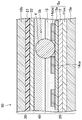
- FIG. 3 is a cross-sectional view of the TFT substrate and a liquid crystal display panel including the TFT substrate along the line III-III in FIG.
- FIG. 4 is an enlarged plan view of a region where the TFT is formed on the TFT substrate.
- FIG. 5 is a cross-sectional view of a liquid crystal display panel in which a short-circuit defect has occurred between the source electrode and the common electrode.
- FIG. 6 is a cross-sectional view of a liquid crystal display panel in which a short-circuit defect has occurred between the source electrode and the drain electrode.
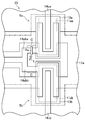
- FIG. 7 is a plan view of the TFT substrate illustrating the method for manufacturing the liquid crystal display panel according to the first embodiment.
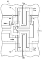
- FIG. 8 is a plan view of a TFT substrate showing a method for manufacturing a liquid crystal display panel according to Embodiment 2.
- FIG. 7 is a plan view of the TFT substrate illustrating the method for manufacturing the liquid crystal display panel according to the first embodiment.
- FIG. 8 is a plan view of a TFT substrate showing a method for manufacturing a liquid crystal display panel according to Embodiment 2.
- FIG. 8 is a plan view of a TFT substrate showing a method for manufacturing a liquid crystal display panel according to Embodiment 2.
- Embodiment 1 of the Invention 1 to 7 show Embodiment 1 of a liquid crystal display panel and a method for manufacturing the same according to the present invention.
- FIG. 1 is a plan view of the TFT substrate 20 constituting the liquid crystal display panel 50 of the present embodiment
- FIG. 2 is a plan view of the TFT substrate 20 in which a region A in FIG. 1 is enlarged.
- 3 is a cross-sectional view of the TFT substrate 20 and the liquid crystal display panel 50 including the same along the line III-III in FIG.
- FIG. 4 is an enlarged plan view of a region of the TFT substrate 20 where the first TFT 5a and the second TFT 5b are formed, that is, the vicinity of a region irradiated with laser light when correcting a short-circuit defect.
- the liquid crystal display panel 50 includes a TFT substrate 20 and a counter substrate 30 provided so as to face each other, a liquid crystal layer 40 provided between the TFT substrate 20 and the counter substrate 30, and a TFT substrate. 20 and the counter substrate 30 are bonded to each other, and a sealing material (not shown) for sealing the liquid crystal layer 40 between the TFT substrate 20 and the counter substrate 30 is provided.
- a sealing material (not shown) for sealing the liquid crystal layer 40 between the TFT substrate 20 and the counter substrate 30 is provided.
- first sub-pixels Pa and A plurality of pixels P having the second sub-pixel Pb are provided in a matrix.
- the TFT substrate 20 is respectively formed on the transparent substrate 10a so as to extend in parallel between the transparent substrate 10a and the first subpixel Pa and the second subpixel Pb of each pixel P.
- a plurality of capacitors provided on the transparent substrate 10a so as to extend in parallel with each other between the provided gate lines 11a and the pixels P in the extending direction of the gate lines 11a (lateral direction in FIG. 1).
- a plurality of first source lines 14a provided so as to extend in parallel with each other between the pixels 11 in a direction (vertical direction in FIG. 1) perpendicular to the gate lines 11a and the capacitor lines 11b.
- a plurality of second source lines 14b that extend in parallel to each other between the pixels P in a direction orthogonal to the gate lines 11a and the capacitor lines 11b and are adjacent to the first source lines 14a, respectively.
- the capacitor line 11b is provided in a two-row lattice form between a pair of adjacent gates 11a.
- the first TFT 5a includes a first gate electrode 11aa provided as a part of the gate line 11a on the transparent substrate 10a and a gate insulation provided so as to cover the first gate electrode 11aa.
- a first source electrode 14aba and a first drain electrode 14ca provided to face each other.
- the first source electrode 14 ab is drawn out from the first source line 14 a or the second source line 14 b along the gate line 11 a, and then on the first subpixel Pa side. It is a portion branched in a U-shape.
- the portion of the first source line 14a or the second source line 14b that is led out along the gate line 11a is gated by the first source line 14a or the second source line 14b.
- the lead portion 14ab extends along the line 11a.
- each first subpixel Pa the first drain electrode 14ca is extended in a + -shape around the center thereof, and an interlayer insulation is formed in the center of the portion extended in the + -shape.
- the auxiliary capacitor of each first subpixel Pa is configured by being connected to the first pixel electrode 16a through the contact hole 15a formed in the film 15 and overlapping the capacitor line 11b through the gate insulating film 12. is doing.
- the second TFT 5b includes a second gate electrode 11ab provided as a part of the gate line 11a on the transparent substrate 10a and a gate insulation provided so as to cover the second gate electrode 11ab.
- a second source electrode 14abb and a second drain electrode 14cb provided to face each other.
- the second source electrode 14abb is led out along the gate line 11a from the first source line 14a or the second source line 14b to the second subpixel Pa side. It is a portion branched in a U-shape.
- the branch portion 14 abc branches from the lead portion 14 ab to the first source electrode 14 aba and the second source electrode 14 abb. .
- each second subpixel Pb the second drain electrode 14cb extends in a + -shape around the center thereof, and an interlayer insulation is formed in the center of the portion extended in the + -shape.
- the auxiliary capacitor of each second subpixel Pb is configured by being connected to the second pixel electrode 16b through the contact hole 15a formed in the film 15 and overlapping the capacitor line 11b through the gate insulating film 12. is doing.
- the first TFT 5a and the second TFT 5b have source lines (first source line 14a and second source different from each other) that are adjacent to each other along a direction orthogonal to the gate line 11a (vertical direction in the drawing).
- the connection structure of the first TFT 5a and the second TFT 5b and the first source line 14a or the second source line 14b is arranged in a staggered manner. That is, as shown in FIG. 1, the first TFT 5a and the second TFT 5b on the lower right side in the drawing are connected to the first source line 14a extending in the center in the drawing and are adjacent to each other along the vertical direction in the drawing.
- the first TFT 5a and the second TFT 5b on the upper right side in the drawing are connected to the second source line 14b extending on the right side in the drawing, and the first TFT 5a and the second TFT 5b on the lower left side in the drawing are the second source extending in the center in the drawing.
- a first TFT 5a and a second TFT 5b on the upper left side in the figure that are connected to the line 14b and are adjacent to each other along the vertical direction in the figure are connected to a first source line 14a that extends to the left side in the figure.
- the gate line 11a includes a branched portion of the first source line 14a and the second source line 14b (a branched portion 14abc between the first source electrode 14aba and the second source electrode 14abb). , A single lead-out portion (drawing portion 14ab) opens.
- the first gate electrode 11aa and the second gate electrode 11ab are separated from each other through the open region of the gate line 11a.
- the first source electrode 14aba and the second source electrode 14abb are to be cut in a line shape of 3 ⁇ m or more so as not to overlap the first semiconductor layer 13a and the second semiconductor layer 13b, respectively.
- Each has C.
- specific dimensions in the vicinity of the first TFT 5a and the second TFT 5b are illustrated.
- Da is about 10 ⁇ m
- Db is about 15 ⁇ m
- Dc is about 6 ⁇ m
- Dd is 7 ⁇ m.
- De is about 4 ⁇ m
- Df is about 7 ⁇ m
- Dg is about 10 ⁇ m
- Dh is about 4.5 ⁇ m.
- Each size of the first subpixel Pa and the second subpixel Pb is about 375 ⁇ m long ⁇ about 250 ⁇ m wide.
- the counter substrate 30 includes a transparent substrate 10 b, a black matrix 21 provided in a frame shape on the transparent substrate 10 b and in a lattice shape in the frame, and between the lattices of the black matrix 21.
- a plurality of colored layers such as a red layer, a green layer and a blue layer provided, a common electrode 22 provided so as to cover the black matrix 21 and each colored layer, and a columnar shape provided on the common electrode 22
- a plurality of photo spacers (not shown) and an alignment film (not shown) provided so as to cover the common electrode and each photo spacer.
- the liquid crystal layer 40 is made of a nematic liquid crystal material having electro-optical characteristics, and includes liquid crystal molecules having negative dielectric anisotropy ( ⁇ ⁇ 0).
- the liquid crystal display panel 50 having the above-described configuration is provided for each pixel P in the liquid crystal layer 40 disposed between each first pixel electrode 16 a and each second pixel electrode 16 b on the TFT substrate 20 and the common electrode 22 on the counter substrate 30.
- the transmittance of light transmitted through the panel is adjusted for each pixel P, and an image is displayed.
- the first subpixel Pa and the second subpixel Pb of each pixel P are individually driven, so that the luminance of the first subpixel Pa and the second subpixel Pb of each pixel P is increased. It is controlled to be different from each other.
- FIG. 5 is a cross-sectional view of the liquid crystal display panel 50 in which a short-circuit defect Sa has occurred between the first source electrode 14 aba and the common electrode 22.
- FIG. 6 is a cross-sectional view of the liquid crystal display panel 50 in which a short-circuit defect Sb has occurred between the first source electrode 14aba and the first drain electrode 14ca.
- FIG. 7 is a plan view of the TFT substrate 20 showing a method for manufacturing the liquid crystal display panel 50 of the present embodiment.
- the manufacturing method of this embodiment includes a TFT substrate manufacturing process, a counter substrate manufacturing process, a bonded body manufacturing process, a defect detection process, and a defect correction process.
- ⁇ TFT substrate manufacturing process> First, a titanium film (thickness of about 25 nm) and a copper film (thickness of about 400 nm) are sequentially formed on the entire substrate of the transparent substrate 10a such as a glass substrate by, for example, sputtering to form a metal laminated film. After that, the metal laminated film is subjected to photolithography, etching, and resist pattern peeling cleaning to form the gate line 11a having the first gate electrode 11aa and the second gate electrode 11ab, and the capacitor line 11b. .
- a silicon nitride film (having a thickness of about 400 nm) or the like is formed on the entire substrate on which the gate lines 11a and the capacitor lines 11b are formed, for example, by plasma CVD (Chemical Vapor Deposition) method. Form.
- an intrinsic amorphous silicon film (thickness of about 200 nm) and phosphorus-doped n + amorphous silicon film (thickness of about 20 nm) are formed on the entire substrate on which the gate insulating film 12 is formed, for example, by plasma CVD.
- the first and second gate electrodes 11aa and 11ab are removed by performing photolithography, etching, and resist pattern peeling cleaning on the intrinsic amorphous silicon film and the n + amorphous silicon film.
- An island-shaped first semiconductor layer forming layer (13a) and a second semiconductor layer forming layer (13b) are formed above.
- a titanium film (thickness of about 30 nm) and a copper film (thickness) are formed on the entire substrate on which the first semiconductor layer formation layer (13a) and the second semiconductor layer formation layer (13b) are formed, for example, by sputtering.
- a metal laminated film is formed, and then the metal laminated film is subjected to photolithography, etching, and resist pattern peeling cleaning, whereby the first source electrode 14aba and the first A first source line 14a having two source electrodes 14abb, a second source line 14b having first and second source electrodes 14abb, 14abb, a first drain electrode 14ca, and a second drain electrode 14cb are formed.
- the first semiconductor layer 13a and the first TFT 5a including the first semiconductor layer 13a, and the second semiconductor layer 13b and the second TFT 5b including the first semiconductor layer 13b are formed.
- a silicon nitride film (thickness of about 200 nm) or the like is formed on the entire substrate on which the first TFT 5a and the second TFT 5b are formed by, for example, a plasma CVD method to form an inorganic insulating film.
- an acrylic photosensitive resin film is applied to the entire substrate on which the inorganic insulating film has been formed, for example, by a spin coating method or a slit coating method, and the applied photosensitive resin film is exposed to light. Then, by performing development and baking, an organic insulating film (thickness of about 2500 nm) having an opening serving as a part of the contact hole 15a is formed above the first drain electrode 14ca and the second drain electrode 14cb.
- the inorganic insulating film exposed from the opening of the organic insulating film is removed by etching to form a contact hole 15a, thereby forming an interlayer insulating film 15 composed of a laminated film of the inorganic insulating film and the organic insulating film. To do.
- the first pixel electrode 16a and the second pixel electrode 16b are formed by performing photolithography, etching, and resist pattern peeling and cleaning.
- an alignment film material film is applied to the entire substrate on which the first pixel electrode 16a and the second pixel electrode 16b are formed by, for example, a spin coating method or a slit coating method, and the applied alignment film material is applied to the alignment film material. Then, an alignment film (having a thickness of about 100 nm) is formed by performing exposure, development, and baking.
- the alignment film material film is formed of, for example, a thin film of a polymer organic compound configured such that a side chain is inclined in the irradiation direction of UV light by irradiation with UV (ultraviolet) light for a certain period of time.
- the TFT substrate 20 can be manufactured as described above.
- an acrylic photosensitive resin colored in black is applied to the entire substrate of the transparent substrate 10b such as a glass substrate by, for example, a spin coating method or a slit coating method, and the applied photosensitive resin is applied to a photomask.
- the black matrix 21 (thickness of about 2 ⁇ m) is formed by developing after exposure through the film.
- an acrylic photosensitive resin colored in red, green or blue is applied to the substrate on which the black matrix 21 is formed by, for example, spin coating or slit coating, and the applied photosensitive property is applied.
- the resin is exposed through a photomask and then patterned by development to form a colored layer (for example, a red layer) of a selected color with a thickness of about 2 ⁇ m. Further, the same process is repeated for the other two colors to form other two colored layers (for example, a green layer and a blue layer) with a thickness of about 2 ⁇ m.
- an ITO film (thickness of about 100 nm) is formed on the substrate on which each of the colored layers is formed by, for example, a sputtering method to form the common electrode 22.
- a photo spacer (thickness of about 1 ⁇ m) is formed by performing exposure, development, and baking.
- an alignment film material film is applied to the entire substrate on which the photo spacer is formed, for example, by spin coating or slit coating, and the applied alignment film material is exposed, developed and baked. By doing so, an alignment film (thickness of about 100 nm) is formed.
- the counter substrate 30 can be manufactured as described above.
- ⁇ Bonded body production process First, for example, after a seal material made of a UV curing and thermosetting resin or the like is printed in a frame shape on the surface of the counter substrate 30 manufactured in the counter substrate manufacturing step, a liquid crystal material is placed inside the seal material. Is dripped.
- the counter substrate 30 onto which the liquid crystal material has been dropped and the TFT substrate 20 manufactured in the TFT substrate manufacturing process are bonded together under reduced pressure, and then the bonded bonded body is released to atmospheric pressure. By pressing, the surface and the back surface of the bonded body are pressurized.
- the sealing material is cured by heating the bonded body.
- the unnecessary part is removed by dividing the bonding body which hardened the above-mentioned sealing material, for example by dicing.
- the liquid crystal display panel 50 (bonding body) can be produced as described above.
- a predetermined inspection signal is applied to each gate line 11 a, each capacitance line 11 b, each first source line 14 a, each second source line 14 b, and the common electrode 22 for the liquid crystal display panel 50 manufactured in the bonded body manufacturing process.
- the defect Sa is detected.
- the short-circuit defect Sa is generated when the foreign matter F that causes the short-circuit defect Sb generated between the first source electrode 14 aba and the first drain electrode 14 ca transports the liquid crystal display panel. It is thought that this occurs due to movement due to vibration of the panel or pressure applied to the panel surface.
- the laser light L is applied to the Ra portion of the first source electrode 14aba in the first subpixel P in which the short-circuit defect Sa has been detected.
- the first TFT 5a is separated from the first source line 14a by irradiating and cutting the first source electrode 14aba at the cut portion C.
- the laser light L is output with a spot size of about 1 ⁇ m ⁇ 5 ⁇ m using, for example, a YAG (Yttrium Aluminum Garnet) laser.
- the capacitance line 11b and the first drain electrode 14ca are connected by laser light irradiation, thereby blackening the first subpixel Pa.
- the liquid crystal display panel 50 in which the short-circuit defect Sa of the present embodiment is corrected can be manufactured.
- each first source line 14a or each second source line 14a in the TFT substrate 20 manufactured in the TFT substrate manufacturing process, in each pixel P, each first source line 14a or each second source line 14a.
- each gate line 11a is opened at a branched portion of each first source line 14a or each second source line 14b, that is, a portion of the first source electrode 14aba and the second source electrode 14abb.
- the first source of the first TFT 5a on the TFT substrate 20 side in each pixel P of the liquid crystal display panel 50 in the bonded body manufactured in the bonded body manufacturing step When a short-circuit defect Sa in which the electrode 14aba or the second source electrode 14abb of the second TFT 5b and the common electrode 22 of the counter substrate 20 are short-circuited is detected, the short-circuit defect Sa is detected in the defect correction process.
- the first source electrode 14 aba or the second source electrode 14 abb that is short-circuited is cut by irradiating the laser beam L through the opened portion of each gate line 11 a, and the corresponding first TFT 5 a or second TFT 5 b is changed.
- the TFT is separated from the first source line 14a or the second source line 14b to which the TFT is connected. Thereby, in the pixel P in which the short-circuit defect Sa is detected, the signal input to the common electrode 22 is not input to the first source line 14a or the second source line 14b, so that each TFT ( The short-circuit defect Sa generated between the source electrode (first source electrode 14aba and second source electrode 14abb) of the first TFT 5a and the second TFT 5b) and the common electrode 22 of the counter substrate 30 can be corrected.
- the defect correction step the portion (first source electrode 14 aba or second source electrode 14 abb) irradiated with the laser beam L when correcting the short-circuit defect Sa is the first source line 14 a or the second source line.
- each first source line 14a or each second source line 14b by irradiation with the laser beam L and each The damage of the gate line 11a can be suppressed, and for example, the short-circuit defect can be corrected more easily than when the TFT is arranged in the vicinity of the portion where the source line and the gate line intersect. Therefore, a short circuit generated between the source electrode (first source electrode 14 aba and second source electrode 14 abb) of each TFT (first TFT 5 a and second TFT 5 b) provided on the TFT substrate 20 and the common electrode 22 of the counter substrate 30.
- the defect Sa can be corrected as easily as possible.
- each gate line 11a is opened at a single drawn portion of each first source line 14a or each second source line 14b. 11a and the area where each first source line 14a and each second source line 14b overlap can be suppressed and formed at the intersection of each gate line 11a and each first source line 14a and each second source line 14b. Parasitic capacitance can be reduced.
- the first source electrode 14aba has the cut portion C formed in a line shape of 3 ⁇ m or more so as not to overlap the first semiconductor layer 13a
- the second source Since the electrode 14abb has the cut portions C formed in a linear shape of 3 ⁇ m or more so as not to overlap the second semiconductor layer 13b, a laser is applied to each cut portion C when correcting the short-circuit defect Sa.
- the short-circuited first source electrode 14aba or second source electrode 14abb can be reliably cut.
- each first TFT 5a and each second TFT 5b are provided in an intermediate portion between the first source line 14a and the second source line 14b adjacent via the pixel P.
- a portion (first source electrode 14 aba or second source electrode 14 abb) irradiated with laser light L when correcting the short-circuit defect Sa intersects with each gate line 11 a of each first source line 14 a or each second source line 14 b. It can be specifically spaced from the portion extending in the direction of the movement.
- a + -shaped dark portion is centered on the center of each first subpixel Pa and each second subpixel Pb Therefore, using the dark portion, the first TFT 5a and the second TFT 5b, the capacitor line 11b, and the extended portions of the first drain electrode 14ca and the second drain electrode 14cb overlapping the capacitor line 11b are formed. By disposing, it is possible to suppress a decrease in the aperture ratio of each pixel P due to the disposition of the auxiliary capacitor.
- the liquid crystal display panel 50 of the present embodiment in the pixel P in which the short-circuit defect Sa is corrected, the first subpixel Pa becomes a black spot, but the second subpixel Pb is normally driven.
- the display quality can be improved as compared with the case where the whole is blackened.
- FIG. 8 is a plan view of the TFT substrate 20a showing the method for manufacturing the liquid crystal display panel 50 of the present embodiment.
- the same parts as those in FIGS. 1 to 7 are denoted by the same reference numerals, and detailed description thereof is omitted.
- the manufacturing method of the liquid crystal display panel 50 in which the laser beam L for cutting is irradiated to one place with respect to the pixel P in which the short-circuit defect Sa is detected is illustrated.
- a method of manufacturing the liquid crystal display panel 50 in which the cutting laser beam L is irradiated to three locations on the pixels P where Sa is detected will be exemplified.
- the first source electrode in the first subpixel P in which the short circuit defect Sa is detected as shown in FIG.
- the first source electrode 14aba is cut at the cut portion C
- the gate line 11a is cut into the first gate electrode 11aa.
- the first TFT 5a is separated from the first source line 14a and the gate line 11a by cutting at the front side and the rear side.
- the capacitance line 11b and the first drain electrode 14ca are connected by laser light irradiation, thereby blackening the first subpixel Pa.
- the liquid crystal display panel 50 in which the short-circuit defect Sa of the present embodiment is corrected can be manufactured.
- each pixel P in the TFT substrate 20 manufactured in the TFT substrate manufacturing process, in each pixel P, as in the first embodiment.
- 1 source line 14a or each 2nd source line 14b is drawn out along each gate line 11a, and then branches to the 1st subpixel Pa side, and the 1st source electrode 14aba branched to the 2nd subpixel Pb side Second gate electrode 11abb, and each gate line 11a is opened at each first source line 14a or a branched portion of each second source line 14b, that is, at the first source electrode 14abb and the second source electrode 14abb.
- the source electrodes (first source electrode 14aba and second source electrode) of each TFT (first TFT 5a and second TFT 5b) provided on the TFT substrate 20 are provided. And 14abb), it can be as much as possible easily correct the short-circuit defect Sa generated between the common electrode 22 of the counter substrate 30.
- the first gate electrode 11aa corresponding to the shorted first source electrode 14aba is connected to the gate line to which the first gate electrode 11aa is connected. 11a, the electrical connection between the first TFT 5a of the first subpixel Pa in which the short-circuit defect Sa has occurred and the corresponding gate line 11a and first source line 14a is released, so that the first TFT 5a Problems caused by the short-circuit defect Sa can be reduced.
- a liquid crystal display panel including a TFT has been exemplified.
- the present invention can also be applied to a liquid crystal display panel including a three-terminal switching element other than a TFT.
- the manufacturing method for correcting the short-circuit defect after the lighting inspection is exemplified.
- the present invention is applied to the array inspection using the charge detection method for the TFT substrate manufactured in the TFT substrate manufacturing process. After detecting the short-circuit defect generated between the source electrode and the drain electrode of the TFT and correcting the short-circuit defect, the source electrode of each TFT which is concerned after being panelized and the common electrode of the counter substrate It can apply also to the manufacturing method which suppresses generation
- a liquid crystal display panel including a bottom gate TFT has been exemplified.
- the present invention can also be applied to a liquid crystal display panel including a top gate TFT.
- the liquid crystal display panel including the TFT substrate in which the two source lines of the first source line and the second source line are provided between the pixels is illustrated.
- the present invention can also be applied to a liquid crystal display panel including a TFT substrate in which one source line is provided between pixels.
- the liquid crystal display panel including the TFT substrate having the TFT electrode connected to the pixel electrode as the drain electrode has been exemplified.
- the TFT electrode connected to the pixel electrode is used as the source.
- the present invention can also be applied to a liquid crystal display panel including a TFT substrate called an electrode.
- the liquid crystal provided with the liquid crystal display panel is provided. Useful for TVs.
Landscapes
- Physics & Mathematics (AREA)
- Nonlinear Science (AREA)
- Engineering & Computer Science (AREA)
- Microelectronics & Electronic Packaging (AREA)
- Mathematical Physics (AREA)
- Chemical & Material Sciences (AREA)
- Crystallography & Structural Chemistry (AREA)
- General Physics & Mathematics (AREA)
- Optics & Photonics (AREA)
- Liquid Crystal (AREA)
- Manufacturing & Machinery (AREA)
- Thin Film Transistor (AREA)
Abstract
液晶表示パネルを構成するTFT基板(20)では、互いに隣り合う第1副画素及び第2副画素を有する各画素において、各画素の間に延びる各ソース線(14a)が各画素の第1副画素及び第2副画素の間に延びる各ゲート線(11a)に沿って単一に引き出された後に第1副画素側に分岐して各第1TFT(5a)の一部を構成する第1ソース電極(14aba)と、第2副画素側に分岐して各第2TFT(5b)の一部を構成する第2ソース電極(14abb)とを有し、各ゲート線(11a)が各ソース線(14a)の分岐した部分で開口している。
Description
本発明は、液晶表示パネル及びその製造方法に関し、特に、薄膜トランジスタ基板を備えた液晶表示パネルにおいて、薄膜トランジスタ基板の各薄膜トランジスタのソース電極と、対向基板の共通電極との間に発生した短絡欠陥を修正する技術に関するものである。
アクティブマトリクス駆動方式の液晶表示パネルは、例えば、画像の最小単位である各画素毎に、薄膜トランジスタ(Thin Film Transistor、以下、「TFT」とも称する)、及びTFTに接続された画素電極を有するTFT基板と、TFT基板に対向するように設けられ、共通電極を有する対向基板と、TFT基板の各画素電極及び対向基板の共通電極の間に設けられた液晶層とを備えている。ここで、多くのTFT基板では、各画素の液晶層、すなわち、各画素の液晶容量に充電された電荷を安定に保持するために、各画素毎に補助容量が設けられている。
例えば、特許文献1には、液晶表示パネルの色ずれを防止するために、マトリクス状に配列された(上記画素に相当する)各単位画素を複数の副画素領域に分割し、各副画素領域に(上記TFTに相当する)アクティブ素子、(上記液晶容量に相当する)液晶キャパシタ、及び(上記補助容量に相当する)蓄積キャパシタを配置し、同一単位画素内において、副画素領域における蓄積キャパシタと液晶キャパシタとの容量比を副画素領域毎に異ならせた液晶表示パネルが開示されている。
ところで、TFT基板を備えた液晶表示パネルでは、各画素のTFTにおいて、ソース電極及びドレイン電極の間に導電性を有する異物が介在すると、ソース電極及びドレイン電極の間が短絡して、その画素が正常に動作しなくなるおそれがあるので、例えば、基板検査工程において、各画素のTFTの何れかでソース電極及びドレイン電極の間が短絡した短絡欠陥が検出された場合には、修正工程において、レーザー光の照射により、短絡欠陥が検出された画素の画素電極と、短絡したドレイン電極とを切り離して黒点化することが多い。
しかしながら、上記修正工程において、短絡欠陥が検出された画素の画素電極と、短絡したドレイン電極とを切り離しても、液晶表示パネルを運搬する際の振動やパネル表面に対する加圧などに起因して、ソース電極及びドレイン電極の間を短絡させていた異物を介して、TFT基板側の短絡した又は短絡していたソース電極と、対向基板側の共通電極との間が短絡するおそれがある。また、上記基板検査工程において、短絡欠陥として検出されないレベルであっても、仮に、ソース電極及びドレイン電極の間に導電性を有する異物が潜在していれば、液晶表示パネルを運搬する際の振動やパネル表面に対する加圧などにより、ソース電極及びドレイン電極の間に潜在する異物が顕在化して、TFT基板側のソース電極と、対向基板側の共通電極との間が短絡するおそれもある。なお、特許文献1に開示された液晶表示パネルのように、ゲート線及びソース線の交差する部分の近傍にTFTが設けられた液晶表示パネルでは、上記修正工程において、レーザー光を照射する際に、TFTに接続されたゲート線及びソース線を損傷させるおそれがあるので、改善の余地がある。
本発明は、かかる点に鑑みてなされたものであり、その目的とするところは、薄膜トランジスタ基板の各薄膜トランジスタのソース電極と、対向基板の共通電極との間に発生した短絡欠陥を可及的に容易に修正することにある。
上記目的を達成するために、本発明は、各画素において、各ソース線が各ゲート線に沿って単一に引き出された後に第1副画素側に分岐した第1ソース電極と、第2副画素側に分岐した第2ソース電極とを備えるようにしたものである。
具体的に本発明に係る液晶表示パネルは、互いに隣り合う第1副画素及び第2副画素を有する画素と、該第1副画素及び第2副画素の間に配置されたゲート線と、該ゲート線と交差する方向の上記画素の縁に沿って配置されたソース線と、上記第1副画素に設けられた第1薄膜トランジスタと、該第1薄膜トランジスタに設けられた第1ソース電極と、上記第2副画素に設けられた第2薄膜トランジスタと、該第2薄膜トランジスタに設けられた第2ソース電極とを備えた薄膜トランジスタ基板と、上記薄膜トランジスタ基板に対向して設けられ、共通電極を有する対向基板と、上記薄膜トランジスタ基板及び対向基板の間に設けられた液晶層とを備え、上記ソース線は、上記ゲート線に沿って延びる引き出し部、及び該引き出し部から上記第1ソース電極と上記第2ソース電極とに分岐する分岐部を有し、上記ゲート線は、上記分岐部で開口している。
上記の構成によれば、ソース線がゲート線に沿って延びる引き出し部、及び引き出し部から第1ソース電極と第2ソース電極とに分岐する分岐部を有し、ゲート線がソース線の分岐部で開口しているので、液晶表示パネルの各画素において、薄膜トランジスタ基板側の第1薄膜トランジスタの第1ソース電極、又は第2薄膜トランジスタの第2ソース電極と、対向基板の共通電極との間が短絡した短絡欠陥が検出された場合には、短絡欠陥が検出された画素において、ゲート線の開口した部分を介してレーザー光を照射することにより、短絡した第1ソース電極又は第2ソース電極を切断して、対応する第1薄膜トランジスタ又は第2薄膜トランジスタをその薄膜トランジスタが接続されたソース線から分離することになる。これにより、短絡欠陥が検出された画素において、共通電極に入力される信号がソース線に入力されなくなるので、薄膜トランジスタ基板に設けられた薄膜トランジスタのソース電極と、対向基板の共通電極との間に発生した短絡欠陥が修正される。ここで、短絡欠陥を修正する際にレーザー光を照射する箇所(第1ソース電極又は第2ソース電極に分岐する分岐部)は、各ソース線の各ゲート線と交差する方向に延びる部分から離間していると共に、ゲート線に重なっていないので、レーザー光の照射によるソース線及びゲート線の損傷が抑制され、例えば、薄膜トランジスタがソース線及びゲート線の交差する部分の近傍に配置された場合よりも短絡欠陥が容易に修正される。したがって、薄膜トランジスタ基板の薄膜トランジスタのソース電極と、対向基板の共通電極との間に発生した短絡欠陥を可及的に容易に修正することが可能になる。
また、本発明に係る液晶表示パネルは、各々、互いに隣り合うように配置された第1副画素及び第2副画素を有し、マトリクス状に設けられた複数の画素と、該各画素の第1副画素及び第2副画素の間に、互いに平行に延びるようにそれぞれ設けられた複数のゲート線と、該各ゲート線と交差する方向の該各画素の間に、互いに平行に延びるようにそれぞれ設けられた複数のソース線と、上記各画素の第1副画素毎にそれぞれ設けられた複数の第1薄膜トランジスタと、上記各画素の第2副画素毎にそれぞれ設けられた複数の第2薄膜トランジスタとを備えた薄膜トランジスタ基板と、上記薄膜トランジスタ基板に対向するように設けられ、共通電極を有する対向基板と、上記薄膜トランジスタ基板及び対向基板の間に設けられた液晶層とを備え、上記薄膜トランジスタ基板は、上記各画素において、上記各ソース線が上記各ゲート線に沿って単一に引き出された後に上記第1副画素側に分岐して上記各第1薄膜トランジスタの一部を構成する第1ソース電極と、上記第2副画素側に分岐して上記各第2薄膜トランジスタの一部を構成する第2ソース電極とを有し、上記各ゲート線は、上記各ソース線の分岐した部分で開口している。
上記の構成によれば、各画素において、各ソース線が各ゲート線に沿って単一に引き出された後に第1副画素側に分岐した第1ソース電極と、第2副画素側に分岐した第2ソース電極とを備え、各ゲート線が各ソース線の分岐した部分、すなわち、第1ソース電極及び第2ソース電極の部分で開口しているので、液晶表示パネルの各画素において、薄膜トランジスタ基板側の第1薄膜トランジスタの第1ソース電極、又は第2薄膜トランジスタの第2ソース電極と、対向基板の共通電極との間が短絡した短絡欠陥が検出された場合には、短絡欠陥が検出された画素において、各ゲート線の開口した部分を介してレーザー光を照射することにより、短絡した第1ソース電極又は第2ソース電極を切断して、対応する第1薄膜トランジスタ又は第2薄膜トランジスタをその薄膜トランジスタが接続されたソース線から分離することになる。これにより、短絡欠陥が検出された画素において、共通電極に入力される信号がソース線に入力されなくなるので、薄膜トランジスタ基板に設けられた各薄膜トランジスタのソース電極と、対向基板の共通電極との間に発生した短絡欠陥が修正される。ここで、短絡欠陥を修正する際にレーザー光を照射する箇所(第1ソース電極又は第2ソース電極)は、各ソース線の各ゲート線と交差する方向に延びる部分から離間していると共に、ゲート線に重なっていないので、レーザー光の照射による各ソース線及び各ゲート線の損傷が抑制され、例えば、薄膜トランジスタがソース線及びゲート線の交差する部分の近傍に配置された場合よりも短絡欠陥が容易に修正される。したがって、薄膜トランジスタ基板の各薄膜トランジスタのソース電極と、対向基板の共通電極との間に発生した短絡欠陥を可及的に容易に修正することが可能になる。
上記各ゲート線は、上記各ソース線の単一に引き出された部分で開口していてもよい。
上記の構成によれば、各ゲート線が各ソース線の単一に引き出された部分で開口しているので、各ゲート線と各ソース線との重なる面積が抑制され、各ゲート線と各ソース線との交差部分に形成される寄生容量が小さくなる。
上記各第1薄膜トランジスタは、島状に設けられた第1半導体層を有し、上記第1ソース電極は、上記第1半導体層に重ならないように3μm以上の線状に形成された被切断部を有し、上記各第2薄膜トランジスタは、島状に設けられた第2半導体層を有し、上記第2ソース電極は、上記第2半導体層に重ならないように3μm以上の線状に形成された被切断部を有していてもよい。
上記の構成によれば、第1ソース電極が第1半導体層に重ならないように3μm以上の線状に形成された被切断部を有し、第2ソース電極が第2半導体層に重ならないように3μm以上の線状に形成された被切断部を有しているので、短絡欠陥を修正する際には、各被切断部にレーザー光を照射することにより、短絡した第1ソース電極又は第2ソース電極が確実に切断される。
上記各第1薄膜トランジスタ及び各第2薄膜トランジスタは、上記隣り合う一対のソース線の中間部分に設けられていてもよい。
上記の構成によれば、各第1薄膜トランジスタ及び各第2薄膜トランジスタが隣り合う一対のソース線の中間部分に設けられているので、短絡欠陥を修正する際にレーザー光を照射する箇所(第1ソース電極又は第2ソース電極)が、各ソース線の各ゲート線と交差する方向に延びる部分から具体的に離間される。また、例えば、液晶分子の配向をピコメートルレベルで精密に制御する光配向技術を適用した液晶表示パネルでは、各副画素の中央を中心に+字状の暗部が形成されるので、その暗部を利用して、各第1薄膜トランジスタ及び各第2薄膜トランジスタを始め、容量線、並びに容量線に重なるドレイン電極の延設部を配置することにより、補助容量の配置に起因する各画素の開口率の低下が抑制される。
また、本発明に係る液晶表示パネルの製造方法は、各々、互いに隣り合うように配置された第1副画素及び第2副画素を有し、マトリクス状に設けられた複数の画素と、該各画素の第1副画素及び第2副画素の間に、互いに平行に延びるようにそれぞれ設けられた複数のゲート線と、該各ゲート線と交差する方向の該各画素の間に、互いに平行に延びるようにそれぞれ設けられた複数のソース線と、上記各画素の第1副画素毎にそれぞれ設けられた複数の第1薄膜トランジスタと、上記各画素の第2副画素毎にそれぞれ設けられた複数の第2薄膜トランジスタとを備え、上記各画素において、上記各ソース線が上記各ゲート線に沿って単一に引き出された後に上記第1副画素側に分岐して上記各第1薄膜トランジスタの一部を構成する第1ソース電極と、上記第2副画素側に分岐して上記各第2薄膜トランジスタの一部を構成する第2ソース電極とを有し、上記各ゲート線が上記各ソース線の分岐した部分で開口した薄膜トランジスタ基板を作製する薄膜トランジスタ基板作製工程と、共通電極を有する対向基板を作製する対向基板作製工程と、上記薄膜トランジスタ基板作製工程で作製された薄膜トランジスタ基板、及び上記対向基板作製工程で作製された対向基板を液晶層を介して貼り合わせることにより、貼合体を作製する貼合体作製工程と、上記貼合体作製工程で作製された貼合体の各画素において、上記第1ソース電極又は第2ソース電極と上記共通電極との間が短絡した短絡欠陥を検出する欠陥検出工程と、上記欠陥検出工程で短絡欠陥が検出された画素において、上記各ゲート線の開口した部分を介してレーザー光を照射することにより、上記短絡した第1ソース電極又は第2ソース電極を切断して、対応する上記第1薄膜トランジスタ又は第2薄膜トランジスタを該薄膜トランジスタが接続されたソース線から分離する欠陥修正工程とを備える。
上記の方法によれば、薄膜トランジスタ基板作製工程で作製された薄膜トランジスタ基板では、各画素において、各ソース線が各ゲート線に沿って単一に引き出された後に第1副画素側に分岐した第1ソース電極と、第2副画素側に分岐した第2ソース電極とを備え、各ゲート線が各ソース線の分岐した部分、すなわち、第1ソース電極及び第2ソース電極の部分で開口しているので、欠陥検出工程において、貼合体作製工程で作製された貼合体、すなわち、液晶表示パネルの各画素において、薄膜トランジスタ基板側の第1薄膜トランジスタの第1ソース電極、又は第2薄膜トランジスタの第2ソース電極と、対向基板の共通電極との間が短絡した短絡欠陥が検出された場合には、欠陥修正工程において、短絡欠陥が検出された画素において、各ゲート線の開口した部分を介してレーザー光を照射することにより、短絡した第1ソース電極又は第2ソース電極を切断して、対応する第1薄膜トランジスタ又は第2薄膜トランジスタをその薄膜トランジスタが接続されたソース線から分離することになる。これにより、短絡欠陥が検出された画素において、共通電極に入力される信号がソース線に入力されなくなるので、薄膜トランジスタ基板に設けられた各薄膜トランジスタのソース電極と、対向基板の共通電極との間に発生した短絡欠陥が修正される。ここで、欠陥修正工程において、短絡欠陥を修正する際にレーザー光を照射する箇所(第1ソース電極又は第2ソース電極)は、各ソース線の各ゲート線と交差する方向に延びる部分から離間していると共に、ゲート線に重なっていないので、レーザー光の照射による各ソース線及び各ゲート線の損傷が抑制され、例えば、薄膜トランジスタがソース線及びゲート線の交差する部分の近傍に配置された場合よりも短絡欠陥が容易に修正される。したがって、薄膜トランジスタ基板の各薄膜トランジスタのソース電極と、対向基板の共通電極との間に発生した短絡欠陥を可及的に容易に修正することが可能になる。
上記薄膜トランジスタ基板は、上記各画素において、上記各ゲート線が上記各第1薄膜トランジスタの一部を構成する第1ゲート電極と、該第1ゲート電極から離間して上記各第2薄膜トランジスタの一部を構成する第2ゲート電極とを有し、上記欠陥修正工程では、上記短絡した第1ソース電極又は第2ソース電極に対応する上記第1ゲート電極又は第2ゲート電極を該ゲート電極が接続されたゲート線から分離してもよい。
上記の方法によれば、欠陥修正工程では、短絡した第1ソース電極又は第2ソース電極に対応する第1ゲート電極又は第2ゲート電極をそのゲート電極が接続されたゲート線から分離するので、短絡欠陥が発生した副画素の薄膜トランジスタと、それに対応するゲート線及びソース線との電気的な接続が解除されることにより、薄膜トランジスタの短絡欠陥に起因する不具合が低減される。
本発明によれば、各画素において、各ソース線が各ゲート線に沿って単一に引き出された後に第1副画素側に分岐した第1ソース電極と、第2副画素側に分岐した第2ソース電極とを備えているので、薄膜トランジスタ基板の各薄膜トランジスタのソース電極と、対向基板の共通電極との間に発生した短絡欠陥を可及的に容易に修正することができる。
以下、本発明の実施形態を図面に基づいて詳細に説明する。なお、本発明は、以下の各実施形態に限定されるものではない。
《発明の実施形態1》
図1~図7は、本発明に係る液晶表示パネル及びその製造方法の実施形態1を示している。具体的に、図1は、本実施形態の液晶表示パネル50を構成するTFT基板20の平面図であり、図2は、図1中の領域Aを拡大したTFT基板20の平面図である。また、図3は、図2中のIII-III線に沿ったTFT基板20及びそれを備えた液晶表示パネル50の断面図である。さらに、図4は、TFT基板20における第1TFT5a及び第2TFT5bが形成された領域、すなわち、短絡欠陥を修正する際にレーザー光が照射される領域の近傍を拡大した平面図である。
図1~図7は、本発明に係る液晶表示パネル及びその製造方法の実施形態1を示している。具体的に、図1は、本実施形態の液晶表示パネル50を構成するTFT基板20の平面図であり、図2は、図1中の領域Aを拡大したTFT基板20の平面図である。また、図3は、図2中のIII-III線に沿ったTFT基板20及びそれを備えた液晶表示パネル50の断面図である。さらに、図4は、TFT基板20における第1TFT5a及び第2TFT5bが形成された領域、すなわち、短絡欠陥を修正する際にレーザー光が照射される領域の近傍を拡大した平面図である。
液晶表示パネル50は、図3に示すように、互いに対向するように設けられたTFT基板20及び対向基板30と、TFT基板20及び対向基板30の間に設けられた液晶層40と、TFT基板20及び対向基板30を互いに接着すると共に、TFT基板20及び対向基板30の間に液晶層40を封入するためのシール材(不図示)とを備えている。ここで、TFT基板20、対向基板30及びそれらを備えた液晶表示パネル50では、図1に示すように、各々、図中の縦方向に互いに隣り合うように配置された第1副画素Pa及び第2副画素Pbを有する複数の画素Pがマトリクス状に設けられている。
TFT基板20は、図1~図3に示すように、透明基板10aと、各画素Pの第1副画素Pa及び第2副画素Pbの間に互いに平行に延びるように透明基板10a上にそれぞれ設けられた複数のゲート線11aと、各ゲート線11aの延びる方向(図1中の横方向)の各画素Pの間に互いに平行に延びるように透明基板10a上にそれぞれ設けられた複数の容量線11bと、各ゲート線11a及び各容量線11bと直交する方向(図1中の縦方向)の各画素Pの間に互いに平行に延びるようにそれぞれ設けられた複数の第1ソース線14aと、各ゲート線11a及び各容量線11bと直交する方向の各画素Pの間に互いに平行に延びると共に、各第1ソース線14aと隣り合うようにそれぞれ設けられた複数の第2ソース線14bと、各第1副画素Pa毎にそれぞれ設けられた複数の第1TFT5aと、各第2副画素Pb毎にそれぞれ設けられた複数の第2TFT5bと、各第1TFT5a及び各第2TFT5bを覆うように設けられた層間絶縁膜15と、各第1副画素Paにおいて層間絶縁膜15上にそれぞれ設けられ、各第1TFT5aに接続された複数の第1画素電極16aと、各第2副画素Pbにおいて層間絶縁膜15上にそれぞれ設けられ、各第2TFT5bに接続された複数の第2画素電極16bと、各第1画素電極16a及び各第2画素電極16bを覆うように設けられた配向膜(不図示)とを備えている。
容量線11bは、図1に示すように、隣り合う一対のゲート11aの間で2列の格子状に設けられている。
第1TFT5aは、図1~図3に示すように、透明基板10a上にゲート線11aの一部として設けられた第1ゲート電極11aaと、第1ゲート電極11aaを覆うように設けられたゲート絶縁膜12と、ゲート絶縁膜12上に第1ゲート電極11aaに重なるように島状に設けられた第1半導体層13aと、第1半導体層13a上に第1ゲート電極11aaに重なると共に、互いに離間及び対峙するように設けられた第1ソース電極14aba及び第1ドレイン電極14caとを備えている。
第1ソース電極14abaは、図1及び図2に示すように、第1ソース線14a又は第2ソース線14bからゲート線11aに沿って単一に引き出された後に、第1副画素Pa側にU字状に分岐された部分である。ここで、第1ソース線14a又は第2ソース線14bからゲート線11aに沿って単一に引き出された部分は、図2に示すように、第1ソース線14a又は第2ソース線14bがゲート線11aに沿って延びる引き出し部14abになっている。
第1ドレイン電極14caは、図1に示すように、各第1副画素Paにおいて、その中央を中心に+字状に延設され、その+字状に延設された部分の中央で層間絶縁膜15に形成されたコンタクトホール15aを介して第1画素電極16aに接続されていると共に、ゲート絶縁膜12を介して容量線11bに重なることにより、各第1副画素Paの補助容量を構成している。
第2TFT5bは、図1~図3に示すように、透明基板10a上にゲート線11aの一部として設けられた第2ゲート電極11abと、第2ゲート電極11abを覆うように設けられたゲート絶縁膜12と、ゲート絶縁膜12上に第2ゲート電極11abに重なるように島状に設けられた第2半導体層13bと、第2半導体層13b上に第2ゲート電極11abに重なると共に、互いに離間及び対峙するように設けられた第2ソース電極14abb及び第2ドレイン電極14cbとを備えている。
第2ソース電極14abbは、図1及び図2に示すように、第1ソース線14a又は第2ソース線14bからゲート線11aに沿って単一に引き出された後に、第2副画素Pa側にU字状に分岐された部分である。ここで、第1ソース電極14aba及び第2ソース電極14abbの間は、図2に示すように、引き出し部14abから第1ソース電極14aba及び第2ソース電極14abbに分岐する分岐部14abcとなっている。
第2ドレイン電極14cbは、図1に示すように、各第2副画素Pbにおいて、その中央を中心に+字状に延設され、その+字状に延設された部分の中央で層間絶縁膜15に形成されたコンタクトホール15aを介して第2画素電極16bに接続されていると共に、ゲート絶縁膜12を介して容量線11bに重なることにより、各第2副画素Pbの補助容量を構成している。
第1TFT5a及び第2TFT5bは、図1に示すように、ゲート線11aと直交する方向(図中の縦方向)に沿って隣り合うもの同士が互いに異なるソース線(第1ソース線14a及び第2ソース線14b)に接続されており、第1TFT5a及び第2TFT5bと第1ソース線14a又は第2ソース線14bとの接続構造が千鳥状に配置されている。すなわち、図1に示すように、図中の右下側の第1TFT5a及び第2TFT5bは、図中の中央に延びる第1ソース線14aに接続され、それらに図中の縦方向に沿って隣り合う図中の右上側の第1TFT5a及び第2TFT5bは、図中の右側に延びる第2ソース線14bに接続され、図中の左下側の第1TFT5a及び第2TFT5bは、図中の中央に延びる第2ソース線14bに接続され、それらに図中の縦方向に沿って隣り合う図中の左上側の第1TFT5a及び第2TFT5bは、図中の左側に延びる第1ソース線14aに接続されている。
ゲート線11aは、図1及び図2に示すように、第1ソース線14a及び第2ソース線14bの分岐した部分(第1ソース電極14aba及び第2ソース電極14abbの間の分岐部14abc)と、単一に引き出された部分(引き出し部14ab)とで開口している。ここで、第1ゲート電極11aa及び第2ゲート電極11abは、図1及び図2に示すように、ゲート線11aの開口した領域を介して互いに離間している。
第1ソース電極14aba及び第2ソース電極14abbは、図2に示すように、第1半導体層13a及び第2半導体層13bにそれぞれ重ならないように、3μm以上に線状に形成された被切断部Cをそれぞれ有している。ここで、第1TFT5a及び第2TFT5bの近傍の具体的な寸法を例示すると、図4に示すように、Daが10μm程度であり、Dbが15μm程度であり、Dcが6μm程度であり、Ddが7μm程度であり、Deが4μm程度であり、Dfが7μm程度であり、Dgが10μm程度であり、Dhが4.5μm程度である。なお、第1副画素Pa及び第2副画素Pbの各大きさは、縦375μm程度×横250μm程度である。
対向基板30は、図3に示すように、透明基板10bと、透明基板10b上に枠状に且つその枠内に格子状に設けられたブラックマトリクス21と、ブラックマトリクス21の各格子間にそれぞれ設けられた赤色層、緑色層及び青色層などの複数の着色層(不図示)と、ブラックマトリクス21及び各着色層を覆うように設けられた共通電極22と、共通電極22上に柱状に設けられた複数のフォトスペーサ(不図示)と、共通電極及び各フォトスペーサを覆うように設けられた配向膜(不図示)とを備えている。
液晶層40は、電気光学特性を有するネマチックの液晶材料などにより構成され、負の誘電率異方性(Δε<0)の液晶分子を含んでいる。
上記構成の液晶表示パネル50は、TFT基板20上の各第1画素電極16a及び各第2画素電極16bと対向基板30上の共通電極22との間に配置する液晶層40に各画素P毎に所定の電圧を印加して、液晶層40の配向状態を変えることにより、各画素P毎にパネル内を透過する光の透過率を調整して、画像を表示するように構成されている。ここで、液晶表示パネル50では、各画素Pの第1副画素Pa及び第2副画素Pbを個別に駆動させることにより、各画素Pの第1副画素Pa及び第2副画素Pbにおける輝度を互いに異ならせるように制御されている。
次に、本実施形態の液晶表示パネル50を製造する方法について説明する。ここで、図5は、第1ソース電極14aba及び共通電極22の間に短絡欠陥Saが発生した液晶表示パネル50の断面図である。また、図6は、第1ソース電極14aba及び第1ドレイン電極14caの間に短絡欠陥Sbが発生した液晶表示パネル50の断面図である。さらに、図7は、本実施形態の液晶表示パネル50の製造方法を示すTFT基板20の平面図である。なお、本実施形態の製造方法は、TFT基板作製工程、対向基板作製工程、貼合体作製工程、欠陥検出工程及び欠陥修正工程を備える。
<TFT基板作製工程>
まず、ガラス基板などの透明基板10aの基板全体に、例えば、スパッタリング法により、チタン膜(厚さ25nm程度)及び銅膜(厚さ400nm程度)などを順に成膜して、金属積層膜を形成した後に、その金属積層膜に対して、フォトリソグラフィ、エッチング及びレジストパターンの剥離洗浄を行うことにより、第1ゲート電極11aa及び第2ゲート電極11abを有するゲート線11a、並びに容量線11bを形成する。
まず、ガラス基板などの透明基板10aの基板全体に、例えば、スパッタリング法により、チタン膜(厚さ25nm程度)及び銅膜(厚さ400nm程度)などを順に成膜して、金属積層膜を形成した後に、その金属積層膜に対して、フォトリソグラフィ、エッチング及びレジストパターンの剥離洗浄を行うことにより、第1ゲート電極11aa及び第2ゲート電極11abを有するゲート線11a、並びに容量線11bを形成する。
続いて、ゲート線11a及び容量線11bが形成された基板全体に、例えば、プラズマCVD(Chemical Vapor Deposition)法により、窒化シリコン膜(厚さ400nm程度)などを成膜して、ゲート絶縁膜12を形成する。
さらに、ゲート絶縁膜12が形成された基板全体に、例えば、プラズマCVD法により、例えば、真性アモルファスシリコン膜(厚さ200nm程度)、及びリンがドープされたn+アモルファスシリコン膜(厚さ20nm程度)を順に成膜した後に、真性アモルファスシリコン膜及びn+アモルファスシリコン膜の積層膜に対して、フォトリソグラフィ、エッチング及びレジストパターンの剥離洗浄を行うことにより、第1ゲート電極11aa及び第2ゲート電極11abの上方に島状の第1半導体層形成層(13a)及び第2半導体層形成層(13b)をそれぞれ形成する。
続いて、上記第1半導体層形成層(13a)及び第2半導体層形成層(13b)が形成された基板全体に、例えば、スパッタリング法により、チタン膜(厚さ30nm程度)及び銅膜(厚さ400nm程度)などを順に成膜して、金属積層膜を形成した後に、その金属積層膜に対して、フォトリソグラフィ、エッチング及びレジストパターンの剥離洗浄を行うことにより、第1ソース電極14aba及び第2ソース電極14abbを有する第1ソース線14a、第1ソース電極14aba及び第2ソース電極14abbを有する第2ソース線14b、第1ドレイン電極14ca、並びに第2ドレイン電極14cbを形成する。
そして、第1ソース電極14aba及び第1ドレイン電極14ca、並びに第2ソース電極14abb及び第2ドレイン電極14cbをマスクとして、上記第1半導体層形成層(13a)及び第2半導体層形成層(13b)のn+アモルファスシリコン層をエッチングで除去することにより、第1半導体層13a及びそれを備えた第1TFT5a、並びに第2半導体層13b及びそれを備えた第2TFT5bを形成する。
さらに、第1TFT5a及び第2TFT5bが形成された基板全体に、例えば、プラズマCVD法により、窒化シリコン膜(厚さ200nm程度)などを成膜し、無機絶縁膜を形成する。
続いて、上記無機絶縁膜が形成された基板全体に、例えば、スピンコート法又はスリットコート法により、アクリル系の感光性樹脂膜を塗布し、その塗布された感光性樹脂膜に対して、露光、現像及びベーキングを行うことにより、第1ドレイン電極14ca及び第2ドレイン電極14cbの上方にコンタクトホール15aの一部となる開口部を有する有機絶縁膜(厚さ2500nm程度)を形成する。
さらに、上記有機絶縁膜の開口部から露出する上記無機絶縁膜をエッチングで除去して、コンタクトホール15aを形成することにより、無機絶縁膜及び有機絶縁膜の積層膜からなる層間絶縁膜15を形成する。
そして、層間絶縁膜15が形成された基板全体に、例えば、スパッタリング法により、ITO(Indium Tin Oxide)膜(厚さ100nm程度)などの透明導電膜を成膜した後に、その透明導電膜に対して、フォトリソグラフィ、エッチング及びレジストパターンの剥離洗浄を行うことにより、第1画素電極16a及び第2画素電極16bを形成する。
最後に、第1画素電極16a及び第2画素電極16bが形成された基板全体に、例えば、スピンコート法又はスリットコート法により、配向膜材料膜を塗布し、その塗布された配向膜材料に対して、露光、現像及びベーキングを行うことにより、配向膜(厚さ100nm程度)を形成する。ここで、配向膜材料膜は、例えば、一定時間のUV(ultraviolet)光の照射により側鎖がUV光の照射方向に傾くように構成された高分子有機化合物の薄膜により形成されている。
以上のようにして、TFT基板20を作製することができる。
<対向基板作製工程>
まず、ガラス基板などの透明基板10bの基板全体に、例えば、スピンコート法又はスリットコート法により、黒に着色されたアクリル系の感光性樹脂を塗布し、その塗布された感光性樹脂をフォトマスクを介して露光した後に、現像することにより、ブラックマトリクス21(厚さ2μm程度)を形成する。
まず、ガラス基板などの透明基板10bの基板全体に、例えば、スピンコート法又はスリットコート法により、黒に着色されたアクリル系の感光性樹脂を塗布し、その塗布された感光性樹脂をフォトマスクを介して露光した後に、現像することにより、ブラックマトリクス21(厚さ2μm程度)を形成する。
続いて、ブラックマトリクス21が形成された基板上に、例えば、スピンコート法又はスリットコート法により、赤、緑又は青に着色されたアクリル系の感光性樹脂を塗布し、その塗布された感光性樹脂をフォトマスクを介して露光した後に、現像することによりパターニングして、選択した色の着色層(例えば、赤色層)を厚さ2μm程度に形成する。さらに、他の2色についても同様な工程を繰り返して、他の2色の着色層(例えば、緑色層及び青色層)を厚さ2μm程度に形成する。
その後、上記各着色層が形成された基板上に、例えば、スパッタリング法により、ITO膜(厚さ100nm程度)を成膜して、共通電極22を形成する。
さらに、共通電極22が形成された基板全体に、例えば、スピンコート法又はスリットコート法により、感光性のアクリル樹脂などからなる感光性樹脂膜を塗布した後に、その感光性樹脂膜に対して、露光、現像及びベーキングを行うことにより、フォトスペーサ(厚さ1μm程度)を形成する。
最後に、上記フォトスペーサが形成された基板全体に、例えば、スピンコート法又はスリットコート法により、配向膜材料膜を塗布し、その塗布された配向膜材料に対して、露光、現像及びベーキングを行うことにより、配向膜(厚さ100nm程度)を形成する。
以上のようにして、対向基板30を作製することができる。
<貼合体作製工程>
まず、例えば、上記対向基板作製工程で作製された対向基板30の表面に、UV硬化及び熱硬化の併用型樹脂などからなるシール材を枠状に印刷した後に、そのシール材の内側に液晶材料を滴下する。
まず、例えば、上記対向基板作製工程で作製された対向基板30の表面に、UV硬化及び熱硬化の併用型樹脂などからなるシール材を枠状に印刷した後に、そのシール材の内側に液晶材料を滴下する。
続いて、上記液晶材料が滴下された対向基板30と、上記TFT基板作製工程で作製されたTFT基板20とを、減圧下で貼り合わせた後に、その貼り合わせた貼合体を大気圧に開放することにより、その貼合体の表面及び裏面を加圧する。
さらに、上記貼合体に挟持されたシール材にUV光を照射した後に、その貼合体を加熱することによりシール材を硬化させる。
最後に、上記シール材を硬化させた貼合体を、例えば、ダイシングにより分断することにより、その不要な部分を除去する。
以上のようにして、液晶表示パネル50(貼合体)を作製することができる。
<欠陥検出工程>
上記貼合体作製工程で作製された液晶表示パネル50に対して、各ゲート線11a、各容量線11b、各第1ソース線14a、各第2ソース線14b及び共通電極22に所定の検査信号を入力して、点灯検査を行うことにより、例えば、図5に示すように、膜残りなどの導電性を有する異物Fを介して、第1ソース電極14abaと共通電極22との間が短絡した短絡欠陥Saを検出する。ここで、短絡欠陥Saは、例えば、図6に示すように、第1ソース電極14aba及び第1ドレイン電極14caの間で発生した短絡欠陥Sbを引き起こした異物Fが、液晶表示パネルを運搬する際の振動やパネル表面に対する加圧などに起因して移動することにより、発生するものと考えられる。
上記貼合体作製工程で作製された液晶表示パネル50に対して、各ゲート線11a、各容量線11b、各第1ソース線14a、各第2ソース線14b及び共通電極22に所定の検査信号を入力して、点灯検査を行うことにより、例えば、図5に示すように、膜残りなどの導電性を有する異物Fを介して、第1ソース電極14abaと共通電極22との間が短絡した短絡欠陥Saを検出する。ここで、短絡欠陥Saは、例えば、図6に示すように、第1ソース電極14aba及び第1ドレイン電極14caの間で発生した短絡欠陥Sbを引き起こした異物Fが、液晶表示パネルを運搬する際の振動やパネル表面に対する加圧などに起因して移動することにより、発生するものと考えられる。
<欠陥修正工程>
上記欠陥検出工程で短絡欠陥Saが検出された場合には、図7に示すように、短絡欠陥Saが検出された第1副画素Pにおいて、第1ソース電極14abaのRa部にレーザー光Lを照射することにより、第1ソース電極14abaを被切断部Cで切断することにより、第1ソース線14aから第1TFT5aを分離する。ここで、レーザー光Lは、例えば、YAG(Yttrium Aluminium Garnet)レーザーなどを用いて、1μm×5μm程度のスポットサイズで出力されたものである。その後、第1TFT5aが分離された第1副画素Pにおいて、レーザー光の照射により、容量線11bと第1ドレイン電極14caとを接続することにより、当該第1副画素Paを黒点化する。
上記欠陥検出工程で短絡欠陥Saが検出された場合には、図7に示すように、短絡欠陥Saが検出された第1副画素Pにおいて、第1ソース電極14abaのRa部にレーザー光Lを照射することにより、第1ソース電極14abaを被切断部Cで切断することにより、第1ソース線14aから第1TFT5aを分離する。ここで、レーザー光Lは、例えば、YAG(Yttrium Aluminium Garnet)レーザーなどを用いて、1μm×5μm程度のスポットサイズで出力されたものである。その後、第1TFT5aが分離された第1副画素Pにおいて、レーザー光の照射により、容量線11bと第1ドレイン電極14caとを接続することにより、当該第1副画素Paを黒点化する。
以上のようにして、本実施形態の短絡欠陥Saが修正された液晶表示パネル50を製造することができる。
以上説明したように、本実施形態の液晶表示パネル50及びその製造方法によれば、TFT基板作製工程で作製されたTFT基板20では、各画素Pにおいて、各第1ソース線14a又は各第2ソース線14bが各ゲート線11aに沿って単一に引き出された後に第1副画素Pa側に分岐した第1ソース電極14abaと、第2副画素Pb側に分岐した第2ソース電極14abbとを備え、各ゲート線11aが各第1ソース線14a又は各第2ソース線14bの分岐した部分、すなわち、第1ソース電極14aba及び第2ソース電極14abbの部分で開口しているので、欠陥検出工程において、貼合体作製工程で作製された貼合体、すなわち、液晶表示パネル50の各画素Pにおいて、TFT基板20側の第1TFT5aの第1ソース電極14aba、又は第2TFT5bの第2ソース電極14abbと、対向基板20の共通電極22との間が短絡した短絡欠陥Saが検出された場合には、欠陥修正工程において、短絡欠陥Saが検出された画素Pにおいて、各ゲート線11aの開口した部分を介してレーザー光Lを照射することにより、短絡した第1ソース電極14aba又は第2ソース電極14abbを切断して、対応する第1TFT5a又は第2TFT5bをそのTFTが接続された第1ソース線14a又は第2ソース線14bから分離することになる。これにより、短絡欠陥Saが検出された画素Pにおいて、共通電極22に入力される信号が第1ソース線14a又は第2ソース線14bに入力されなくなるので、TFT基板20に設けられた各TFT(第1TFT5a及び第2TFT5b)のソース電極(第1ソース電極14aba及び第2ソース電極14abb)と、対向基板30の共通電極22との間に発生した短絡欠陥Saを修正することができる。ここで、欠陥修正工程において、短絡欠陥Saを修正する際にレーザー光Lを照射する箇所(第1ソース電極14aba又は第2ソース電極14abb)は、各第1ソース線14a又は各第2ソース線14bの各ゲート線11aと直交する方向に延びる部分から離間していると共に、ゲート線11aに重なっていないので、レーザー光Lの照射による各第1ソース線14a又は各第2ソース線14b及び各ゲート線11aの損傷を抑制することができ、例えば、TFTがソース線及びゲート線の交差する部分の近傍に配置された場合よりも短絡欠陥を容易に修正することができる。したがって、TFT基板20に設けられた各TFT(第1TFT5a及び第2TFT5b)のソース電極(第1ソース電極14aba及び第2ソース電極14abb)と、対向基板30の共通電極22との間に発生した短絡欠陥Saを可及的に容易に修正することができる。
また、本実施形態の液晶表示パネル50によれば、各ゲート線11aが各第1ソース線14a又は各第2ソース線14bの単一に引き出された部分で開口しているので、各ゲート線11aと各第1ソース線14a及び各第2ソース線14bとの重なる面積を抑制することができ、各ゲート線11aと各第1ソース線14a及び各第2ソース線14bとの交差部分に形成される寄生容量を小さくすることができる。
また、本実施形態の液晶表示パネル50によれば、第1ソース電極14abaが第1半導体層13aに重ならないように3μm以上の線状に形成された被切断部Cを有し、第2ソース電極14abbが第2半導体層13bに重ならないように3μm以上の線状に形成された被切断部Cを有しているので、短絡欠陥Saを修正する際には、各被切断部Cにレーザー光Lを照射することにより、短絡した第1ソース電極14aba又は第2ソース電極14abbを確実に切断することができる。
また、本実施形態の液晶表示パネル50によれば、各第1TFT5a及び各第2TFT5bが画素Pを介して隣り合う第1ソース線14a及び第2ソース線14bの中間部分に設けられているので、短絡欠陥Saを修正する際にレーザー光Lを照射する箇所(第1ソース電極14aba又は第2ソース電極14abb)を、各第1ソース線14a又は各第2ソース線14bの各ゲート線11aと交差する方向に延びる部分から具体的に離間させることができる。また、液晶分子の配向をピコメートルレベルで精密に制御する光配向技術を適用した液晶表示パネル50では、各第1副画素Pa及び各第2副画素Pbの中央を中心に+字状の暗部が形成されるので、その暗部を利用して、各第1TFT5a及び各第2TFT5bを始め、容量線11b、並びに容量線11bに重なる第1ドレイン電極14ca及び第2ドレイン電極14cbの各延設部を配置することにより、補助容量の配置に起因する各画素Pの開口率の低下を抑制することができる。
また、本実施形態の液晶表示パネル50によれば、短絡欠陥Saが修正された画素Pでは、第1副画素Paが黒点化するものの、第2副画素Pbが正常に駆動するので、画素P全体が黒点化する場合よりも表示品位を向上させることができる。
《発明の実施形態2》
図8は、本実施形態の液晶表示パネル50の製造方法を示すTFT基板20aの平面図である。なお、以下の実施形態において、図1~図7と同じ部分については同じ符号を付して、その詳細な説明を省略する。
図8は、本実施形態の液晶表示パネル50の製造方法を示すTFT基板20aの平面図である。なお、以下の実施形態において、図1~図7と同じ部分については同じ符号を付して、その詳細な説明を省略する。
上記実施形態1では、短絡欠陥Saが検出された画素Pに対して、切断用のレーザー光Lを1箇所に照射する液晶表示パネル50の製造方法を例示したが、本実施形態では、短絡欠陥Saが検出された画素Pに対して、切断用のレーザー光Lを3箇所に照射する液晶表示パネル50の製造方法を例示する。
具体的には、欠陥修正工程において、欠陥検出工程で短絡欠陥Saが検出された場合には、図8に示すように、短絡欠陥Saが検出された第1副画素Pにおいて、第1ソース電極14abaのRa部、並びにゲート線11aのRb部及びRc部にレーザー光Lをそれぞれ照射することにより、第1ソース電極14abaを被切断部Cで切断すると共に、ゲート線11aを第1ゲート電極11aaの前側及び後側で切断することにより、第1ソース線14a及びゲート線11aから第1TFT5aを分離する。その後、第1TFT5aが分離された第1副画素Pにおいて、レーザー光の照射により、容量線11bと第1ドレイン電極14caとを接続することにより、当該第1副画素Paを黒点化する。これにより、本実施形態の短絡欠陥Saが修正された液晶表示パネル50を製造することができる。
以上説明したように、本実施形態の液晶表示パネル50及びその製造方法によれば、上記実施形態1と同様に、TFT基板作製工程で作製されたTFT基板20では、各画素Pにおいて、各第1ソース線14a又は各第2ソース線14bが各ゲート線11aに沿って単一に引き出された後に第1副画素Pa側に分岐した第1ソース電極14abaと、第2副画素Pb側に分岐した第2ソース電極14abbとを備え、各ゲート線11aが各第1ソース線14a又は各第2ソース線14bの分岐した部分、すなわち、第1ソース電極14aba及び第2ソース電極14abbの部分で開口しているので、TFT基板20に設けられた各TFT(第1TFT5a及び第2TFT5b)のソース電極(第1ソース電極14aba及び第2ソース電極14abb)と、対向基板30の共通電極22との間に発生した短絡欠陥Saを可及的に容易に修正することができる。
また、本実施形態の液晶表示パネル50の製造方法によれば、欠陥修正工程では、短絡した第1ソース電極14abaに対応する第1ゲート電極11aaをその第1ゲート電極11aaが接続されたゲート線11aから分離するので、短絡欠陥Saが発生した第1副画素Paの第1TFT5aと、それに対応するゲート線11a及び第1ソース線14aとの電気的な接続が解除されることにより、第1TFT5aの短絡欠陥Saに起因する不具合を低減することができる。
なお、上記各実施形態では、TFTを備えた液晶表示パネルを例示したが、本発明は、TFT以外の3端子のスイッチング素子を備えた液晶表示パネルにも適用することができる。
また、上記各実施形態では、点灯検査後に短絡欠陥を修正する製造方法を例示したが、本発明は、TFT基板作製工程で作製されたTFT基板に対して、電荷検出法などを用いたアレイ検査を行い、TFTのソース電極及びドレイン電極の間で発生した短絡欠陥を検出した後に、その短絡欠陥を修正することにより、パネル化した後に懸念される各TFTのソース電極と、対向基板の共通電極との間における短絡欠陥の発生を抑制する製造方法にも適用することができる。
また、上記各実施形態では、ボトムゲート構造のTFTを備えた液晶表示パネルを例示したが、本発明は、トップゲート構造のTFTを備えた液晶表示パネルにも適用することができる。
また、上記各実施形態では、各画素の間に第1ソース線及び第2ソース線の2本のソース線が設けられたTFT基板を備えた液晶表示パネルを例示したが、本発明は、各画素の間に1本のソース線が設けられたTFT基板を備えた液晶表示パネルにも適用することができる。
また、上記各実施形態では、画素電極に接続されたTFTの電極をドレイン電極としたTFT基板を備えた液晶表示パネルを例示したが、本発明は、画素電極に接続されたTFTの電極をソース電極と呼ぶTFT基板を備えた液晶表示パネルにも適用することができる。
以上説明したように、本発明は、TFT基板の各TFTのソース電極と、対向基板の共通電極との間に発生した短絡欠陥を容易に修正することができるので、液晶表示パネルを備えた液晶テレビなどについて有用である。
C 被切断部
L レーザー光
P 画素
Pa 第1副画素
Pb 第2副画素
Sa 短絡欠陥
5a 第1TFT
5b 第2TFT
11a ゲート線
11aa 第1ゲート電極
11ab 第2ゲート電極
13a 第1半導体層
13b 第2半導体層
14a 第1ソース線
14ab 引き出し部
14b 第2ソース線
14aba 第1ソース電極
14abb 第2ソース電極
14abc 分岐部
20 TFT基板
22 共通電極
30 対向基板
40 液晶層
50 液晶表示パネル(貼合体)
L レーザー光
P 画素
Pa 第1副画素
Pb 第2副画素
Sa 短絡欠陥
5a 第1TFT
5b 第2TFT
11a ゲート線
11aa 第1ゲート電極
11ab 第2ゲート電極
13a 第1半導体層
13b 第2半導体層
14a 第1ソース線
14ab 引き出し部
14b 第2ソース線
14aba 第1ソース電極
14abb 第2ソース電極
14abc 分岐部
20 TFT基板
22 共通電極
30 対向基板
40 液晶層
50 液晶表示パネル(貼合体)
Claims (7)
- 互いに隣り合う第1副画素及び第2副画素を有する画素と、該第1副画素及び第2副画素の間に配置されたゲート線と、該ゲート線と交差する方向の上記画素の縁に沿って配置されたソース線と、上記第1副画素に設けられた第1薄膜トランジスタと、該第1薄膜トランジスタに設けられた第1ソース電極と、上記第2副画素に設けられた第2薄膜トランジスタと、該第2薄膜トランジスタに設けられた第2ソース電極とを備えた薄膜トランジスタ基板と、
上記薄膜トランジスタ基板に対向して設けられ、共通電極を有する対向基板と、
上記薄膜トランジスタ基板及び対向基板の間に設けられた液晶層とを備え、
上記ソース線は、上記ゲート線に沿って延びる引き出し部、及び該引き出し部から上記第1ソース電極と上記第2ソース電極とに分岐する分岐部を有し、
上記ゲート線は、上記分岐部で開口している、液晶表示パネル。 - 各々、互いに隣り合うように配置された第1副画素及び第2副画素を有し、マトリクス状に設けられた複数の画素と、該各画素の第1副画素及び第2副画素の間に、互いに平行に延びるようにそれぞれ設けられた複数のゲート線と、該各ゲート線と交差する方向の該各画素の間に、互いに平行に延びるようにそれぞれ設けられた複数のソース線と、上記各画素の第1副画素毎にそれぞれ設けられた複数の第1薄膜トランジスタと、上記各画素の第2副画素毎にそれぞれ設けられた複数の第2薄膜トランジスタとを備えた薄膜トランジスタ基板と、
上記薄膜トランジスタ基板に対向するように設けられ、共通電極を有する対向基板と、
上記薄膜トランジスタ基板及び対向基板の間に設けられた液晶層とを備え、
上記薄膜トランジスタ基板は、上記各画素において、上記各ソース線が上記各ゲート線に沿って単一に引き出された後に上記第1副画素側に分岐して上記各第1薄膜トランジスタの一部を構成する第1ソース電極と、上記第2副画素側に分岐して上記各第2薄膜トランジスタの一部を構成する第2ソース電極とを有し、
上記各ゲート線は、上記各ソース線の分岐した部分で開口している、液晶表示パネル。 - 上記各ゲート線は、上記各ソース線の単一に引き出された部分で開口している、請求項2に記載の液晶表示パネル。
- 上記各第1薄膜トランジスタは、島状に設けられた第1半導体層を有し、
上記第1ソース電極は、上記第1半導体層に重ならないように3μm以上の線状に形成された被切断部を有し、
上記各第2薄膜トランジスタは、島状に設けられた第2半導体層を有し、
上記第2ソース電極は、上記第2半導体層に重ならないように3μm以上の線状に形成された被切断部を有している、請求項2又は3に記載の液晶表示パネル。 - 上記各第1薄膜トランジスタ及び各第2薄膜トランジスタは、上記隣り合う一対のソース線の中間部分に設けられている、請求項2乃至4の何れか1つに記載の液晶表示パネル。
- 各々、互いに隣り合うように配置された第1副画素及び第2副画素を有し、マトリクス状に設けられた複数の画素と、該各画素の第1副画素及び第2副画素の間に、互いに平行に延びるようにそれぞれ設けられた複数のゲート線と、該各ゲート線と交差する方向の該各画素の間に、互いに平行に延びるようにそれぞれ設けられた複数のソース線と、上記各画素の第1副画素毎にそれぞれ設けられた複数の第1薄膜トランジスタと、上記各画素の第2副画素毎にそれぞれ設けられた複数の第2薄膜トランジスタとを備え、上記各画素において、上記各ソース線が上記各ゲート線に沿って単一に引き出された後に上記第1副画素側に分岐して上記各第1薄膜トランジスタの一部を構成する第1ソース電極と、上記第2副画素側に分岐して上記各第2薄膜トランジスタの一部を構成する第2ソース電極とを有し、上記各ゲート線が上記各ソース線の分岐した部分で開口した薄膜トランジスタ基板を作製する薄膜トランジスタ基板作製工程と、
共通電極を有する対向基板を作製する対向基板作製工程と、
上記薄膜トランジスタ基板作製工程で作製された薄膜トランジスタ基板、及び上記対向基板作製工程で作製された対向基板を液晶層を介して貼り合わせることにより、貼合体を作製する貼合体作製工程と、
上記貼合体作製工程で作製された貼合体の各画素において、上記第1ソース電極又は第2ソース電極と上記共通電極との間が短絡した短絡欠陥を検出する欠陥検出工程と、
上記欠陥検出工程で短絡欠陥が検出された画素において、上記各ゲート線の開口した部分を介してレーザー光を照射することにより、上記短絡した第1ソース電極又は第2ソース電極を切断して、対応する上記第1薄膜トランジスタ又は第2薄膜トランジスタを該薄膜トランジスタが接続されたソース線から分離する欠陥修正工程とを備える、液晶表示パネルの製造方法。 - 上記薄膜トランジスタ基板は、上記各画素において、上記各ゲート線が上記各第1薄膜トランジスタの一部を構成する第1ゲート電極と、該第1ゲート電極から離間して上記各第2薄膜トランジスタの一部を構成する第2ゲート電極とを有し、
上記欠陥修正工程では、上記短絡した第1ソース電極又は第2ソース電極に対応する上記第1ゲート電極又は第2ゲート電極を該ゲート電極が接続されたゲート線から分離する、請求項6に記載の液晶表示パネルの製造方法。
Priority Applications (1)
| Application Number | Priority Date | Filing Date | Title |
|---|---|---|---|
| US14/354,084 US9354479B2 (en) | 2011-10-27 | 2012-10-19 | Liquid-crystal panel and manufacturing method thereof |
Applications Claiming Priority (2)
| Application Number | Priority Date | Filing Date | Title |
|---|---|---|---|
| JP2011235653 | 2011-10-27 | ||
| JP2011-235653 | 2011-10-27 |
Publications (1)
| Publication Number | Publication Date |
|---|---|
| WO2013061556A1 true WO2013061556A1 (ja) | 2013-05-02 |
Family
ID=48167412
Family Applications (1)
| Application Number | Title | Priority Date | Filing Date |
|---|---|---|---|
| PCT/JP2012/006723 Ceased WO2013061556A1 (ja) | 2011-10-27 | 2012-10-19 | 液晶表示パネル及びその製造方法 |
Country Status (2)
| Country | Link |
|---|---|
| US (1) | US9354479B2 (ja) |
| WO (1) | WO2013061556A1 (ja) |
Families Citing this family (3)
| Publication number | Priority date | Publication date | Assignee | Title |
|---|---|---|---|---|
| CN104007594B (zh) * | 2014-06-17 | 2017-12-29 | 深圳市华星光电技术有限公司 | Tft阵列基板结构 |
| CN104360554B (zh) * | 2014-11-18 | 2017-07-07 | 深圳市华星光电技术有限公司 | 液晶显示面板及其阵列基板 |
| US10103072B2 (en) | 2016-08-18 | 2018-10-16 | Semiconductor Components Industries, Llc | Damaging components with defective electrical couplings |
Citations (4)
| Publication number | Priority date | Publication date | Assignee | Title |
|---|---|---|---|---|
| JP2004163943A (ja) * | 2002-11-14 | 2004-06-10 | Samsung Electronics Co Ltd | 液晶表示装置用薄膜トランジスタ基板 |
| WO2006064789A1 (ja) * | 2004-12-14 | 2006-06-22 | Sharp Kabushiki Kaisha | 液晶表示装置および液晶表示装置の欠陥修正方法 |
| JP2008089646A (ja) * | 2006-09-29 | 2008-04-17 | Sharp Corp | 表示装置 |
| WO2009001578A1 (ja) * | 2007-06-28 | 2008-12-31 | Sharp Kabushiki Kaisha | アクティブマトリクス基板、液晶パネル、液晶表示ユニット、液晶表示装置、テレビジョン受像機、液晶パネルの製造方法 |
Family Cites Families (10)
| Publication number | Priority date | Publication date | Assignee | Title |
|---|---|---|---|---|
| KR100289538B1 (ko) * | 1998-05-20 | 2001-06-01 | 김순택 | 박막트랜지스터 액정표시소자의 배선 레이아웃 |
| JP3645184B2 (ja) * | 2000-05-31 | 2005-05-11 | シャープ株式会社 | 液晶表示装置及びその欠陥修正方法 |
| US7206048B2 (en) * | 2003-08-13 | 2007-04-17 | Samsung Electronics Co., Ltd. | Liquid crystal display and panel therefor |
| CN100463018C (zh) * | 2005-05-23 | 2009-02-18 | 夏普株式会社 | 有源矩阵衬底、显示装置以及像素缺陷修正方法 |
| US7768604B2 (en) * | 2005-09-20 | 2010-08-03 | Au Optronics Corporation | Transflective liquid crystal display with partially shifted reflectivity curve |
| JP4932823B2 (ja) * | 2006-03-06 | 2012-05-16 | シャープ株式会社 | アクティブマトリクス基板、表示装置及びテレビジョン受像機 |
| TWI364734B (en) | 2006-06-30 | 2012-05-21 | Chimei Innolux Corp | Liquid crystal display panel, driving method and liquid crystal displayer |
| WO2008096483A1 (ja) * | 2007-02-09 | 2008-08-14 | Sharp Kabushiki Kaisha | アクティブマトリクス基板、液晶パネル、液晶表示ユニット、液晶表示装置、テレビジョン受像機、アクティブマトリクス基板の製造方法、液晶パネルの製造方法 |
| JP2009288462A (ja) * | 2008-05-28 | 2009-12-10 | Ips Alpha Technology Ltd | 表示装置及びその製造方法 |
| US8587754B2 (en) * | 2009-06-30 | 2013-11-19 | Samsung Display Co., Ltd. | Liquid crystal display and method of manufacturing the same |
-
2012
- 2012-10-19 US US14/354,084 patent/US9354479B2/en not_active Expired - Fee Related
- 2012-10-19 WO PCT/JP2012/006723 patent/WO2013061556A1/ja not_active Ceased
Patent Citations (4)
| Publication number | Priority date | Publication date | Assignee | Title |
|---|---|---|---|---|
| JP2004163943A (ja) * | 2002-11-14 | 2004-06-10 | Samsung Electronics Co Ltd | 液晶表示装置用薄膜トランジスタ基板 |
| WO2006064789A1 (ja) * | 2004-12-14 | 2006-06-22 | Sharp Kabushiki Kaisha | 液晶表示装置および液晶表示装置の欠陥修正方法 |
| JP2008089646A (ja) * | 2006-09-29 | 2008-04-17 | Sharp Corp | 表示装置 |
| WO2009001578A1 (ja) * | 2007-06-28 | 2008-12-31 | Sharp Kabushiki Kaisha | アクティブマトリクス基板、液晶パネル、液晶表示ユニット、液晶表示装置、テレビジョン受像機、液晶パネルの製造方法 |
Also Published As
| Publication number | Publication date |
|---|---|
| US20140313450A1 (en) | 2014-10-23 |
| US9354479B2 (en) | 2016-05-31 |
Similar Documents
| Publication | Publication Date | Title |
|---|---|---|
| JP5243664B2 (ja) | 液晶表示パネル及びその製造方法、並びにアレイ基板及びその製造方法 | |
| JP4777334B2 (ja) | 液晶表示装置及びその製造方法 | |
| JP4961271B2 (ja) | 液晶表示パネルの製造方法及び液晶表示パネル | |
| US20130023086A1 (en) | Active matrix substrate, display panel provided with same, and method for manufacturing active matrix substrate | |
| CN105607306A (zh) | 制造显示基板的方法、修复显示基板的方法和显示基板 | |
| US8314424B2 (en) | Thin film transistor array substrate, display panel comprising the same, and method for manufacturing thin film transistor array substrate | |
| KR101799938B1 (ko) | 액정표시장치 | |
| US20150138475A1 (en) | Array substrate and liquid crystal display panel provided with same | |
| WO2013061556A1 (ja) | 液晶表示パネル及びその製造方法 | |
| CN110133925B (zh) | 显示面板亮点修补方法及其主动矩阵基板和显示面板 | |
| JP6234232B2 (ja) | 液晶表示パネルおよびそのリペア方法 | |
| JP5379790B2 (ja) | アクティブマトリクス基板及びそれを備えた液晶表示パネル並びにアクティブマトリクス基板の製造方法 | |
| KR102084397B1 (ko) | 액정표시장치의 제조방법 | |
| JP2010165866A (ja) | 薄膜トランジスタ基板の製造方法 | |
| KR101234215B1 (ko) | 액정표시장치 및 그 제조방법 | |
| WO2010086920A1 (ja) | 表示装置の製造方法 | |
| WO2013099191A1 (ja) | アクティブマトリクス基板及び液晶表示装置 | |
| JP2010181482A (ja) | アクティブマトリクス基板及びその製造方法並びに表示装置 | |
| KR20160001875A (ko) | 프린지 필드형 액정표시장치 및 그 제조방법 | |
| CN110931503A (zh) | 元件基板、显示面板以及它们的制造方法 | |
| KR20070004329A (ko) | 표시 장치 및 그 제조 방법 | |
| WO2013183220A1 (ja) | 薄膜トランジスタ基板の製造方法 | |
| KR20110077255A (ko) | 횡전계방식 액정표시장치의 제조방법 | |
| KR20070070397A (ko) | 액정 표시 장치 및 그 제조 방법 |
Legal Events
| Date | Code | Title | Description |
|---|---|---|---|
| 121 | Ep: the epo has been informed by wipo that ep was designated in this application |
Ref document number: 12844585 Country of ref document: EP Kind code of ref document: A1 |
|
| WWE | Wipo information: entry into national phase |
Ref document number: 14354084 Country of ref document: US |
|
| NENP | Non-entry into the national phase |
Ref country code: DE |
|
| 122 | Ep: pct application non-entry in european phase |
Ref document number: 12844585 Country of ref document: EP Kind code of ref document: A1 |
|
| NENP | Non-entry into the national phase |
Ref country code: JP |