WO2013057789A1 - 発光パネルアセンブリ及び照明装置 - Google Patents
発光パネルアセンブリ及び照明装置 Download PDFInfo
- Publication number
- WO2013057789A1 WO2013057789A1 PCT/JP2011/073919 JP2011073919W WO2013057789A1 WO 2013057789 A1 WO2013057789 A1 WO 2013057789A1 JP 2011073919 W JP2011073919 W JP 2011073919W WO 2013057789 A1 WO2013057789 A1 WO 2013057789A1
- Authority
- WO
- WIPO (PCT)
- Prior art keywords
- light
- emitting
- light emitting
- contact
- panels
- Prior art date
- Legal status (The legal status is an assumption and is not a legal conclusion. Google has not performed a legal analysis and makes no representation as to the accuracy of the status listed.)
- Ceased
Links
Images


Classifications
-
- H—ELECTRICITY
- H10—SEMICONDUCTOR DEVICES; ELECTRIC SOLID-STATE DEVICES NOT OTHERWISE PROVIDED FOR
- H10K—ORGANIC ELECTRIC SOLID-STATE DEVICES
- H10K59/00—Integrated devices, or assemblies of multiple devices, comprising at least one organic light-emitting element covered by group H10K50/00
- H10K59/10—OLED displays
-
- H—ELECTRICITY
- H10—SEMICONDUCTOR DEVICES; ELECTRIC SOLID-STATE DEVICES NOT OTHERWISE PROVIDED FOR
- H10K—ORGANIC ELECTRIC SOLID-STATE DEVICES
- H10K59/00—Integrated devices, or assemblies of multiple devices, comprising at least one organic light-emitting element covered by group H10K50/00
- H10K59/10—OLED displays
- H10K59/12—Active-matrix OLED [AMOLED] displays
- H10K59/128—Active-matrix OLED [AMOLED] displays comprising two independent displays, e.g. for emitting information from two major sides of the display
-
- H—ELECTRICITY
- H10—SEMICONDUCTOR DEVICES; ELECTRIC SOLID-STATE DEVICES NOT OTHERWISE PROVIDED FOR
- H10K—ORGANIC ELECTRIC SOLID-STATE DEVICES
- H10K59/00—Integrated devices, or assemblies of multiple devices, comprising at least one organic light-emitting element covered by group H10K50/00
- H10K59/10—OLED displays
- H10K59/12—Active-matrix OLED [AMOLED] displays
- H10K59/131—Interconnections, e.g. wiring lines or terminals
-
- H—ELECTRICITY
- H10—SEMICONDUCTOR DEVICES; ELECTRIC SOLID-STATE DEVICES NOT OTHERWISE PROVIDED FOR
- H10K—ORGANIC ELECTRIC SOLID-STATE DEVICES
- H10K59/00—Integrated devices, or assemblies of multiple devices, comprising at least one organic light-emitting element covered by group H10K50/00
- H10K59/10—OLED displays
- H10K59/17—Passive-matrix OLED displays
- H10K59/179—Interconnections, e.g. wiring lines or terminals
Definitions
- the present invention relates to a light-emitting panel assembly including a plurality of light-emitting panels and a lighting device including the light-emitting panel assembly.
- An illumination device using an organic EL (Electro Luminescence) element as a light source is known.
- An organic EL element lighting device has a feature that it has surface emission and has no restriction on the shape of the light emitting surface, and such a feature cannot be obtained by other lighting devices such as an LED (light emitting diode) lighting device. Further development for the practical use of is expected.
- the lighting device using an organic EL element is often left to emit light for a long period of time in an interior lighting application or the like, and the organic EL element itself generates heat and becomes a high temperature state because of long-time driving.
- the high temperature state of the organic EL element is continued for a long time, the deterioration of the organic EL element is accelerated and the luminance is lowered, and as a result, the lifetime as the element is shortened.
- a lighting device In order to cope with such deterioration of the organic EL element, a plurality of light emitting panels each having an organic EL element are stacked in a magazine, and a spring for pressing the light emitting panel toward the opening of the magazine inside the magazine
- a lighting device has been proposed that includes a spring that presses the electrode of the light-emitting panel against the power feeding unit, emits light from the light-emitting panel positioned in the immediate vicinity of the opening, and emits the light emitted through the opening (Patent Document). 1).
- Patent Document Patent Document
- the plurality of springs are provided in the magazine together with the plurality of light-emitting panels in order to press the light-emitting panel and each electrode.
- the light emitting panel in which the defect has occurred is not a structure that can be easily removed from the magazine.
- the problem to be solved by the present invention is to provide a compact light-emitting panel assembly and a lighting device in which the above-mentioned drawbacks are cited as an example, and the light-emitting panel can be easily replaced. .
- the light emitting panel assembly of the invention according to claim 1 includes at least one organic light emitting element and a pair of input electrodes, and emits light by supplying power to the organic light emitting element via the pair of input electrodes.
- a light-emitting panel including a plurality of surface-emitting light-emitting panels that emit light, wherein the light-emitting surfaces of the plurality of surface-emitting light-emitting panels are overlapped with each other such that the light-emitting surfaces of the surface-emitting light-emitting panels face the same light emission direction.
- Each of the plurality of surface-emitting light-emitting panels includes a substrate on which the organic light-emitting element is formed, a first contact end on one of the main surfaces of the substrate, and a second contact end on the other
- a conductive contact group each of which includes a selected contact pair, and the selected pair of input electrodes are connected to each other, and the selected contact Child pair is surface emitting Different for each light emitting panel, the first contact end portion in one of the adjacent ones of the surface emitting light emitting panels and the second contact end portion in the other are in contact with each other for each conductive contact. It is characterized by that.
- An illumination device includes at least one organic light emitting element and a pair of input electrodes, and emits light by supplying power to the organic light emitting element via the pair of input electrodes.
- a light-emitting panel assembly including a plurality of surface-emitting light-emitting panels that emit light, and the plurality of light-emitting-type light-emitting panels are overlapped with each other so that the light-emitting surfaces of the plurality of surface-emitting light-emitting panels face the same light emission direction
- Each of the plurality of surface-emitting light-emitting panels includes a substrate on which the organic light-emitting element is formed, a first contact end on one of the main surfaces of the substrate, and a second on the other.
- a conductive contact group each having a contact end, and a selected contact pair of the conductive contact group is connected to the pair of input electrodes, respectively, and the selection Contacted pair is said surface
- the lighting device includes a drive circuit that selectively drives the plurality of surface-emitting light-emitting panels through the conductive contacts.
- each of the plurality of surface emitting light emitting panels includes a substrate on which an organic light emitting element is formed, and a main surface of the substrate.
- a conductive contact group each having a first contact end on one side and a second contact end on the other, and a pair of selected contact pairs of the conductive contact group
- the input electrodes are connected to each other, and the selected contact pair is different for each surface emitting light emitting panel, and the first contact end portion on one of the adjacent ones of the surface emitting light emitting panels and the other on the other Since the second contact end is in contact with each conductive contact, a compact light-emitting panel assembly in which a plurality of surface-emitting light-emitting panels are stacked can be provided. Further, when the foreground light emitting panel is deteriorated, if the foremost light emitting panel is removed, the immediately underside light emitting panel appears as a new foremost light emitting panel, so that it
- the plurality of surface-emitting light emitting panels are overlapped with each other between the first contact end portion and the first surface-emitting light emitting panel as described above. Since the two contact end portions are electrically connected to each other, a plurality of surface-emitting light-emitting panels can be selectively selected by simply connecting the conductive contact of any one of the flat-light-emitting light-emitting panels and the drive circuit It is possible to drive, and it is not necessary to wire the drive circuit for each panel on the first electrode and the second electrode of the plurality of surface-emitting light emitting panels. Further, when the frontmost light emitting panel of the light emitting panel assembly is removed, the electrical connection to the removed light emitting panel is also cut off at the same time.
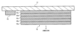
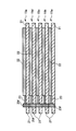
- FIG. 3 is a cross-sectional view taken along the line AB of the light emitting panel assembly of FIG. 2.
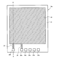
- FIG. 3 is an external view of the light emitting panel assembly of FIG. 2.
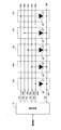
- It is a circuit diagram which shows the connection of the drive circuit of the illuminating device of FIG. 1, and a light emission panel assembly. It is a flowchart which shows the detection operation of the forefront panel by a drive circuit.
- FIG. 1 shows a configuration of a lighting device according to an embodiment of the present invention.
- the illumination device includes a support substrate 11, a light emitting panel assembly 12, and a drive circuit 13.
- the support substrate 11 is a substrate made of, for example, resin that supports the light emitting panel assembly 12 and the drive circuit 13.
- the light emitting panel assembly 12 and the drive circuit 13 are fixed on the support substrate 11 by, for example, adhesion, and the light emission panel assembly 12, the drive circuit 13, and the like are formed by a wiring pattern (not shown) formed on the support substrate 11. Are electrically connected.
- the light-emitting panel assembly 12 has a plurality of light-emitting panels (planar light-emitting type light-emitting panels), in this embodiment, five light-emitting panels 15a to 15e, and the five light-emitting panels 15a to 15e.
- the surface emitting surfaces engage with each other so that their light emitting surfaces face the same light emission direction, and are laminated and fixed.
- Adhesion is performed as an engagement method, and an adhesive material such as an adhesive or a double-sided tape is used for bonding the light emitting panels 15a to 15e.
- the adhesive strength is such that the light emitting panel 15 can be individually peeled off (removed) by human power.
- an engagement method other than adhesion a method using magnetic force or electrostatic force, or a method using a spring can be applied. Further, it may be engaged and fixed using a member such as a screw or a claw as an auxiliary.
- Each of the five light emitting panels 15a to 15e has a substrate 21, a light emitting unit 22, a first electrode line 23, a second electrode line 24, and six contacts 25a to 25f (conducting contact group).
- the substrate 21 is made of a material such as a resin film that is thin and easy to bend.
- inorganic materials such as glass and metal, plastics, and acrylics can be used.
- a material having translucency is usually used as the substrate 21, but in the case of a material having no translucency, It is necessary to provide an opening for light extraction.
- the light-transmitting property of the substrate is not limited.
- the light emitting unit 22 is an organic EL element (organic light emitting element), and includes a cathode (first electrode), an anode (second electrode), and a light emitting functional layer.
- the anode is made of, for example, ITO, is formed on the substrate 21, and is connected to the second electrode line 24.
- a light emitting functional layer is formed on the anode.
- the light-emitting functional layer has a multilayered structure of a hole transport layer, a light-emitting layer, and an electron transport layer in order from the anode side, and can be formed by a dry method such as a vacuum evaporation method, or a wet method such as an inkjet method or printing. It can also be formed by a method.
- ⁇ -NPD can be used as the material of the hole transport layer.
- host CBP and dopant Ir (phq) 2 tpy can be used in the red light emitting layer
- host CBP and dopant HexIr (phq) 3 can be used in the orange light emitting layer
- host CBP in the green light emitting layer
- the dopant Ir (ppy) 3 can be used
- the host PAND and the dopant DPAV can be used in the blue light emitting layer.
- Alq 3 can be used as a material for the electron transport layer.
- a cathode is formed on the light emitting functional layer.
- the cathode can be formed by a vacuum deposition method, and a light reflective metal or alloy such as Al or MgAg is used as the metal material.
- the cathode is connected to the first electrode line 23.
- the internal structure of the light emitting unit 22 is an example, and the present invention is not limited to this.
- the light emission part 22 may be formed from one organic EL element, and may be comprised from several organic EL element.
- the light emitting unit 22 may be sealed with a sealing substrate made of glass or metal, an inorganic film made of silicon nitride, or the like.
- the cathode is the first electrode and the anode is the second electrode.
- the present invention is not limited to this, and the cathode may be the second electrode and the anode may be the first electrode.
- the first electrode line 23 is a line connecting the cathode of the light emitting unit 22 and the contact 25f (first contact), and is formed on the substrate 21 as a pattern.
- the second electrode line 24 is a line that connects the anode of the light emitting unit 22 and any one of the contacts 25a to 25e (a plurality of second contacts), and is formed on the substrate 21 as a pattern.
- the six contacts 25a to 25f are attached to the end of the substrate 21 in that order, and their attachment positions are the same in all the light emitting panels 15a to 15e.
- the contacts 25a to 25f are made of a metal such as copper, have a prismatic shape as shown in FIGS. 3 and 4, and are fixed to the substrate 21 while penetrating the substrate 21.
- Both end portions of the contactors 25a to 25f are contact end portions and have a planar shape.
- the contact end portion on one main surface side (front surface side) where the light emitting portion 22 of the substrate 21 is formed is the first contact end portion, and the contact end portion on the other main surface side (back surface side) is the second contact end. Part.
- a portion that connects the first contact end and the second contact end is a shaft.
- the height of the contacts 25 a to 25 f is substantially equal to the thickness of the light emitting unit 22. There is almost no height of the contacts 25a to 25f on the other main surface side.
- the heads of screws for fixing the contacts 25a to 25f to the substrate 21 may face.
- the contact 25f is for the cathode, and the remaining five contacts 25a to 25e are for the anode.
- the anode contacts 25a to 25e are arranged at equal intervals.
- the cathode contact 25f is arranged slightly apart from the anode contact 25e.
- the cathode contact 25f is connected to the same first electrode line 23 in each of the light emitting panels 15a to 15e.
- the anode contacts 25a to 25e are connected to the second electrode line 24, which are different for each of the light emitting panels 15a to 15e. That is, the contact 25a is connected to the second electrode line 24 in the light emitting panel 15a, the contact 25b is connected to the second electrode line 24 in the light emitting panel 15b, and the contact 25c is connected to the second electrode line 24 in the light emitting panel 15c.
- the contact 25d is connected to the second electrode line 24, and in the light emitting panel 15e, the contact 25e is connected to the second electrode line 24.
- Each of the contacts 25a and 25f, 25b and 25f, 25c and 25f, 25d and 25f, and 25e and 25f is a selected contact pair.
- FIG. 5 is a circuit diagram showing the connection between the drive circuit 13 and each of the light emitting panels 15a to 15e.
- the drive circuit 13 has terminals 13a to 13f, and the terminals 13a to 13e correspond to the light emitting panels 15a to 15a corresponding to each other independently through the connection lines of the anode contacts 25a to 25e.
- the terminal 13e is connected in common to the cathodes of the light emitting units 22 of the light emitting panels 15a to 15e via the connection line of the cathode contact 25f. Therefore, the driving circuit 13 determines the selected contact pair by selecting the connection line to the anode, and can individually drive the light emitting units 22 of the light emitting panels 15a to 15e to emit light.
- the five light emitting panels 15a to 15e can be sequentially peeled off from the frontmost light emitting panel 15a, that is, can be removed, so that the drive circuit 13 drives the light emitting unit 22 of the light emitting panel on the forefront at that time. .
- the drive circuit 13 includes a detection unit that detects which of the light emitting panels 15a to 15e is the light emitting panel on the forefront of the light emitting panel assembly 12. For example, the detection unit can determine the light emitting panel in the forefront in accordance with the electrical continuity between each of the terminals 13a to 13e and the terminal 13f. Next, the operation for discriminating the frontmost light emitting panel according to the electrical conduction state will be described.
- a power supply voltage Vs (for example, 10V) is applied between a terminal 13a and a terminal 13f via a resistor (not shown) (step S1).
- Vs a power supply voltage
- the voltage between the terminal 13a and the terminal 13f is measured, and it is determined whether or not the measured voltage Vm is larger than the threshold voltage Vth (where Vs> Vth) (step S2). If Vm ⁇ Vth, the light emitting panel 15a is in the forefront (step S3), and if Vm> Vth, it is determined that the light emitting panel 15a does not exist.
- the measurement voltage Vm is an applied voltage between the anode and the cathode of the light emitting unit 22 of the light emitting panel 15a.
- the terminal 13a and the terminal 13f are measured. Therefore, the measurement voltage Vm is almost equal to the power supply voltage Vs.
- the power supply voltage Vs is applied between the terminal 13b and the terminal 13f via a resistor (not shown) to determine the presence of the light emitting panel 15b (step S4).
- the voltage between the terminal 13f is measured, and it is determined whether or not the measured voltage Vm is larger than the threshold voltage Vth (step S5).
- steps S7 and S8 are executed to determine the presence of the light emitting panel 15c. If the light emitting panel 15c does not exist, the presence of the light emitting panel 15d is similarly determined. Therefore, steps S10 and S11 are executed, and if the light emitting panel 15d does not exist, steps S13 and S14 are executed in order to determine the presence of the light emitting panel 15e.
- the driving circuit 13 stores the frontmost light emitting panel as data in an internal memory (not shown) (step S16). Thereafter, when light emission driving is instructed from an operation unit (not shown), the drive circuit 13 applies a driving voltage to the light emitting unit 22 of the frontmost light emitting panel at that time, so that the frontmost light emitting panel emits light.
- the detection operation of the light emitting panel in the forefront of the light emitting panel assembly 12 may be executed when a light emission drive is instructed from the operation unit.
- the plurality of flat light emitting panels 15a to 15e are bonded and fixed so as to be peeled off in a state of being overlaid, the plurality of light emitting panels are compactly provided. It can be a light emitting panel assembly. Further, the light emitting panels 15a to 15e of the light emitting panel assembly 12 are bonded to each other, and the foremost light emitting panel can be peeled off by a human hand. Therefore, when the foremost light emitting panel is deteriorated, the removal of the deteriorated panel is completed only by peeling off the foremost light emitting panel. Further, when the frontmost light emitting panel is peeled off, the light emitting panel immediately below it appears as a new frontmost light emitting panel, so that replacement with a new light emitting panel is easy.
- each of the light emitting panels 15a to 15e is made of an organic EL element, for example, by using a resin substrate as the substrate 21, the entire thickness of the light emitting panel assembly 12 including the light emitting panels 15a to 15e is 1 mm or less. It is possible to Further, since each of the light emitting panels 15a to 15e is thin and lightweight, even if a plurality of light emitting panels, for example, five light emitting panels are stacked in the light emitting panel assembly 12 as a spare light emitting panel, the panels are in close contact with each other. Therefore, no useless space is generated, and the entire space is saved.
- the contacts 25a to 25f penetrating the substrate 21 are attached to the same position of the substrate 21, so the light emitting panels 15a to 15e are pasted so that the surface of the substrate 21 faces the same direction. Together, the contacts 25a to 25f at the same position of the light emitting panels 15a to 15e are in a conductive state with each other.
- the cathode contact 25f is common to each of the light emitting panels 15a to 15e, and different contacts for the light emitting panels 15a to 15e are used for the anode contacts 25a to 25e.
- each of the contacts 25 a to 25 f of the light emitting panel 15 e is connected to the drive circuit 13 through the wiring pattern of the support substrate 11. Accordingly, a connection circuit is formed between the light emitting panels 15a to 15e and the driving circuit 13 without any special external wiring, and the driving circuit 13 can individually drive the light emitting panels 15a to 15e. Further, since the drive circuit 13 has a detection function for detecting the presence of each of the light emitting panels 15a to 15e, even if the deteriorated panel is removed, the frontmost light emitting panel at that time can be detected and driven. it can. Therefore, the light emitting panels 15a to 15e are made to emit light sequentially from the panel located at the forefront, and the light emitting panels 15a to 15e can be used efficiently.
- the light-emitting panel that is peeled off when the light-emitting panel is peeled is bent and easily peeled off.
- the contact between the contacts is assured as well as bonding by bonding or Velcro (registered trademark).
- the contacts 25a to 25f are attached through the substrate 21, but it is not always necessary to penetrate the substrate 21.
- one end of the substrate 21 is not provided at the end of the substrate 21.
- Contacts 25a to 25f using detour portions that detour across the substrate 21 between the first contact end portion of the main surface and the other second contact end portion may be attached.
- the contact ends of the contacts 25a to 25f at the same position of the adjacent light emitting panels of the light emitting panel assembly 12 are in contact with each other in a plane, but the contact ends of the contacts 25a to 25f
- the shapes may be complementary to each other, and the substrates may be fixed to each other by engaging the contact end portions of the contact during assembly formation.
- one contact end portion of each of the contacts 25a to 25f has a convex shape, and the other contact end portion has a concave shape. When the light emitting panels are overlapped with each other, the concave and convex portions are fitted and contacted. May be.
- a plurality of substrates may be fixed to each other by a substrate holder, and the contact ends may be maintained in contact with each other.
- the driving circuit 13 has shown a method of electrically discriminating the light emitting panel at the forefront of the light emitting panel assembly 12.
- the light emitting panel optically at the forefront may be discriminated.
- the substrate 21 of each of the light emitting panels 15a to 15e is used as a transparent substrate, and a different reflection pattern for each light emitting panel is formed on the substrate 21, and the optical sensor provided on the support substrate 11 is used.
- the optical sensor provided on the support substrate 11 is used.
- the detection unit for detecting the light emitting panel on the forefront of the light emitting panel assembly 12 is provided in the drive circuit 13, but may be formed separately from the drive circuit 13.
- the cathode contact 25f is used as a single unit and is shared by all the light emitting panels.
- the cathode contacts may be provided by the number of the light emitting panels. That is, if the number of light emitting panels is N (where N is an integer of 2 or more), the number of contacts may be N + 1 or more.
- the light emitting panel of the light emitting panel assembly 12 can be selectively driven to emit light. Since each light emitting panel of the light emitting panel assembly 12 is connected to the drive circuit via the contacts 25a to 25f, the light emitting panel can be arbitrarily switched. In normal use, only the frontmost light-emitting panel emits light, but a plurality of stacked light-emitting panels can emit light simultaneously. For example, it is also possible to obtain white light emission by laminating three light emitting panels that are transparent for both the anode and the cathode and emitting RGB monochromatic light and simultaneously emitting light.
- organic EL elements that emit B (blue) light have a shorter lifetime than organic EL elements that emit RG (red and green) light. Therefore, if the B light emitting panel is arranged on the outermost surface, even if the drive deterioration of B progresses more than RG, it is possible to operate at low cost by replacing only the B light emitting panel.
- the drive circuit 13 drives the second light emitting panel positioned next to the frontmost light emitting panel to emit light. May be.
- the set time corresponds to the total light emission time expected to deteriorate the light emitting panel. Since it is difficult for the user to understand the deterioration of the light-emitting panel, when the total light emission time of the frontmost light-emitting panel reaches the set time, the front light-emitting panel stops emitting light and causes the second light-emitting panel to emit light instead. Thus, the user can be prompted to remove the frontmost light emitting panel. Note that the light emitting state of the second light emitting panel may be lighted or blinked.
- the mutual positional relationship of the conductive contacts in the conductive contact group is at least “equally aligned in one row” between the opposing surfaces of the light emitting panels adjacent to each other.
- the conductive contact groups on the opposing surfaces of the adjacent light emitting panels are formed by setting the same mutual positional relationship such as “positional relationship” or “positional arrangement in a zigzag pattern at a constant pitch”.
- Each contact end portion (the first contact end portion or the second contact end portion) can be in contact with the corresponding contact end portion to form an electric path extending in the stacking direction of the light emitting panel.
- each of the light emitting panels of the conductive contact group there are various possible positions for each of the light emitting panels of the conductive contact group.
- each of at least two conductive contacts is arranged at a position sandwiching the light emitting surface, and around the conductive contact, for example, If the engaging means such as the above-mentioned magic tape is provided, when the light emitting panels are laminated, the mechanical connection of the light emitting panels can be ensured by the engaging means and the corresponding conductive contacts can be reliably and stably connected to each other. Can be guaranteed.
Landscapes
- Electroluminescent Light Sources (AREA)
Abstract
複数の面発光型発光パネルの各々は、有機発光素子が形成された基板と、基板の主面の一方に第1接触端部、及び他方に第2接触端部を各々が有する導通接触子群と、を含み、導通接触子群のうちのいずれかの選択された接触子対と有機発光素子への電力供給のための1対の入力電極とが各々接続されており、選択された接触子対は面発光型発光パネル毎に互いに異なり、面発光型発光パネルの隣接するもの同士のうちの一方における第1接触端部と他方における第2接触端部とが導通接触子毎に接触している発光パネルアセンブリ及びその発光パネルアセンブリの発光パネルを選択的に駆動する駆動回路を備える照明装置。
Description
本発明は、複数の発光パネルからなる発光パネルアセンブリ及びその発光パネルアセンブリを備える照明装置に関する。
発光源として有機EL(Electro Luminescence)素子を用いた照明装置が知られている。有機EL素子の照明装置には、面発光でかつ発光面形状に制約がないという特徴があり、そのような特徴はLED(発光ダイオード)照明装置等の他の照明装置では得られないので、今後の実用化に向けた更なる開発が期待されている。
有機EL素子を用いた照明装置は、室内照明の用途などにおいて長時間に亘って発光させたままにされることが多く、長時間駆動の故に有機EL素子自身が発熱して高温状態になる。ところが、有機EL素子の高温状態の長く継続すると、有機EL素子の劣化が加速されて輝度低下が生じ、その結果、素子としての寿命が短くなることが知られている。
そのような有機EL素子の劣化に対処するために、各々が有機EL素子を有する複数の発光パネルを重ねてマガジンに組み込み、マガジン内部には発光パネルをマガジンの開口部に向けて押しつけるためのバネと共に発光パネルの電極を給電部に押しつけるバネが備えられ、開口部直近に位置した発光パネルが発光してその発光が開口部を介して放出される構成の照明装置が提案されている(特許文献1参照)。この照明装置では開口部直近に位置した発光パネルに欠陥が生じた場合にはその発光パネルをマガジンから取り外すと、それにより新たな良品の発光パネルが開口部に現れるようになっている。
しかしながら、上記のマガジンを備えた照明装置においては、発光パネルと各電極とを押しつけるために複数のバネが複数の発光パネルと共にマガジン内に設けられるためにマガジン自体が大きくなり、その結果、照明装置が大きくなるという欠点があった。また、欠陥が生じた発光パネルをマガジン内から容易に取り外すことが可能な構造ではないという欠点もある。
そこで、本発明が解決しようとする課題は、上記の欠点が一例として挙げられ、本発明の目的は発光パネルを容易に交換することができるコンパクトな発光パネルアセンブリ及び照明装置を提供することである。
請求項1に係る発明の発光パネルアセンブリは、少なくとも1つの有機発光素子と、1対の入力電極とを各々有し、前記1対の入力電極を介した前記有機発光素子への電力供給によって発光面が発光する複数の面発光型発光パネルを含み、前記複数の面発光型発光パネル各々の前記発光面が同一光放出方向を向くように前記複数の発光型発光パネルが互いに重ね合わされた発光パネルアセンブリであって、前記複数の面発光型発光パネルの各々は、前記有機発光素子が形成された基板と、前記基板の主面の一方に第1接触端部、及び他方に第2接触端部を各々が有する導通接触子群と、を含み、前記導通接触子群のうちのいずれかの選択された接触子対と前記1対の入力電極とが各々接続されており、前記選択された接触子対は前記面発光型発光パネル毎に互いに異なり、前記面発光型発光パネルの隣接するもの同士のうちの一方における前記第1接触端部と他方における前記第2接触端部とが前記導通接触子毎に接触していることを特徴としている。
請求項8に係る発明の照明装置は、少なくとも1つの有機発光素子と、1対の入力電極とを各々有し、前記1対の入力電極を介した前記有機発光素子への電力供給によって発光面が発光する複数の面発光型発光パネルを含み、前記複数の面発光型発光パネル各々の前記発光面が同一光放出方向を向くように前記複数の発光型発光パネルが互いに重ね合わされた発光パネルアセンブリを備える照明装置であって、前記複数の面発光型発光パネルの各々は、前記有機発光素子が形成された基板と、前記基板の主面の一方に第1接触端部、及び他方に第2接触端部を各々が有する導通接触子群と、を含み、前記導通接触子群のうちのいずれかの選択された接触子対と前記1対の入力電極とが各々接続されており、前記選択された接触子対は前記面発光型発光パネル毎に互いに異なり、前記面発光型発光パネルの隣接するもの同士のうちの一方における前記第1接触端部と他方における前記第2接触端部とが前記導通接触子毎に接触し、前記照明装置は、前記複数の面発光型発光パネルを前記導通接触子を介して選択的に駆動する駆動回路を含むことを特徴としている。
請求項1に係る発明の発光パネルアセンブリ及び請求項8に係る発明の照明装置によれば、複数の面発光型発光パネルの各々は、有機発光素子が形成された基板と、基板の主面の一方に第1接触端部、及び他方に第2接触端部を各々が有する導通接触子群と、を含み、その導通接触子群のうちのいずれかの選択された接触子対と1対の入力電極とが各々接続されており、選択された接触子対は面発光型発光パネル毎に互いに異なり、面発光型発光パネルの隣接するもの同士のうちの一方における第1接触端部と他方における第2接触端部とが導通接触子毎に接触しているので、複数の面発光型発光パネルを重ね合わせたコンパクトな発光パネルアセンブリを提供することができる。また、最前面の発光パネルが劣化した場合にその最前面の発光パネルを取り去ると、その直下の発光パネルが新たな最前面の発光パネルとして現れるため、新しい発光パネルへの交換が容易である。
更に、請求項8に係る発明の照明装置によれば、複数の面発光型発光パネルは重ね合わされた状態において全ての隣接する平面発光型発光パネル間で上記のように第1接触端部と第2接触端部との接触によって電気的に連結しているので、いずれか1の平面発光型発光パネルの導通接触子と駆動回路とを接続するだけで複数の面発光型発光パネルを選択的に駆動することができ、複数の面発光型発光パネルの第1電極及び第2電極にパネル毎に駆動回路との配線をする必要がない。また、発光パネルアセンブリの最前面の発光パネルを取り去るとその取り去った発光パネルに対する電気的接続も同時に遮断されるという利点もある。
以下、本発明の実施例を、図面を参照しつつ詳細に説明する。
図1は本発明の実施例である照明装置の構成を示している。この照明装置は、支持基板11、発光パネルアセンブリ12、及び駆動回路13を備えている。支持基板11は、発光パネルアセンブリ12及び駆動回路13を支持する、例えば、樹脂からなる基板である。支持基板11上に発光パネルアセンブリ12及び駆動回路13は例えば、接着によって固定されており、また、支持基板11上に形成された配線パターン(図示せず)によって発光パネルアセンブリ12と駆動回路13とは電気的に接続されている。
発光パネルアセンブリ12は図2及び図3に示すように、複数の発光パネル(平面発光型発光パネル)、本実施例では5つの発光パネル15a~15eを有し、その5つの発光パネル15a~15eはその面発光面が同一光放出方向を向くようにして互いに係合して積層固定されている。係合方法として接着が行われており、発光パネル15a~15eの貼り合わせには接着剤や両面テープ等の接着性のある材料が用いられる。ただし、その接着力は人の力で発光パネル15を個別に剥ぎ取る(取り外す)ことができる程度である。接着以外の係合方法として、磁力や静電気力を応用した方法や、バネによる方法を適用することができる。また、補助的にネジやツメ等の部材を用いて係合固定しても良い。
5つの発光パネル15a~15eの各々は基板21、発光部22、第1電極ライン23、第2電極ライン24、及び6つの接触子25a~25f(導通接触子群)を有している。
基板21は薄く曲げやすい樹脂フィルム等の材料からなる。また、ガラスや金属等の無機材料、プラスチック、アクリルを用いることができる。本実施例では、発光部22で生成された光を基板21を介して取り出すので、基板21としては通常、透光性を有する材料が用いられるが、透光性を有しない材料の場合には光取出し用に開口部を設ける必要がある。ただし、基板上方から光を取り出す方式、所謂、トップエミッション方式の有機EL素子の場合、その限りではなく、基板の透光性は問わない。
発光部22は有機EL素子(有機発光素子)であり、陰極(第1電極)、陽極(第2電極)、及び発光機能層からなる。陽極は例えば、ITOからなり、基板21上に形成されており、第2電極ライン24に接続されている。陽極上には発光機能層が形成されている。発光機能層は陽極側から順にホール輸送層、発光層、及び電子輸送層の多層の積層構造を有し、真空蒸着法等のドライ方式で形成することができる他、インクジェット法や印刷等のウェット方式で形成することもできる。ホール輸送層の材料としてはα-NPDを用いることができる。発光層の材料として赤発光層ではホストCBP、ドーパントIr(phq)2tpyを用いることができ、橙発光層ではホストCBP、ドーパントHexIr(phq)3を用いることができ、緑発光層ではホストCBP、ドーパントIr(ppy)3を用いることができ、青発光層ではホストPAND、ドーパントDPAVを用いることができる。電子輸送層の材料としてはAlq3を用いることができる。
発光機能層上には陰極が形成される。陰極は真空蒸着法により形成することができ、金属材料としてはAlやMgAg等の光反射性金属或いは合金が用いられる。陰極は第1電極ライン23に接続されている。
なお、この発光部22の内部構造は一例であり、本発明はこれに限定されない。また、発光部22は、1つの有機EL素子から形成されても良いし、複数の有機EL素子から構成されても良い。更に、発光部22はガラスや金属などからなる封止基板、或いは窒化シリコン等からなる無機膜などによって封止されても良い。また、本実施例では陰極が第1電極であり、陽極が第2電極であるが、これに限定されず、これとは逆に陰極を第2電極とし、陽極を第1電極としても良い。
第1電極ライン23は、発光部22の陰極と接触子25f(第1接触子)とを連結するラインであり、基板21上にパターンとして形成されている。
第2電極ライン24は、発光部22の陽極と接触子25a~25e(複数の第2接触子)のいずれか1つとを連結するラインであり、基板21上にパターンとして形成されている。
6つの接触子25a~25fは基板21の端部にその順番に並んで取り付けられており、それらの取り付け位置は発光パネル15a~15eの全てにおいて同一である。接触子25a~25fは銅等の金属からなり、図3及び図4に示すように角柱形状をしており、基板21を貫通した状態で基板21に固定されている。接触子25a~25fの両端部が接触端部であり、平面形状とされている。基板21の発光部22が形成された一方の主面側(表面側)の接触端部が第1接触端部であり、他方の主面側(裏面側)の接触端部が第2接触端部である。第1接触端部と第2接触端部とを結合する部分がシャフトである。基板21の一方の主面側において接触子25a~25fの高さは発光部22の厚さにほぼ等しい。他方の主面側において接触子25a~25fの高さはほとんどなく、例えば、接触子25a~25fを基板21に固定するためのネジの頭部が面していても良い。
6つの接触子25a~25fのうちの接触子25fが陰極用であり、残りの5つの接触子25a~25eが陽極用である。陽極用の接触子25a~25eは等間隔で配置されている。陰極用の接触子25fは陽極用の接触子25eから若干離れて配置されている。
また、図4に示すように、陰極用の接触子25fは発光パネル15a~15e各々で同じ第1電極ライン23に接続されている。一方、陽極用の接触子25a~25eについては発光パネル15a~15e毎に異なる陽極用の接触子が第2電極ライン24に接続されている。すなわち、発光パネル15aでは接触子25aが第2電極ライン24に接続され、発光パネル15bでは接触子25bが第2電極ライン24に接続され、発光パネル15cでは接触子25cが第2電極ライン24に接続され、発光パネル15dでは接触子25dが第2電極ライン24に接続され、そして、発光パネル15eでは接触子25eが第2電極ライン24に接続されている。接触子25aと25f、25bと25f、25cと25f、25dと25f、及び25eと25fの各々が選択された接触子対である。
図3及び図4に示したように、5つの発光パネル15a~15eを基板21の表面が同一方向を向くように貼り合わせる場合には、発光パネル15a~15eの隣接するパネルの一方の基板21の裏面に他方のパネルの発光部22が接着される。その際に発光パネル15a~15eの隣接するパネル同士で同一位置にある接触子25a~25f各々が互いに接触している。すなわち、隣接するパネル同士のうちの一方における第1接触端部と他方における第2接触端部とが導通接触子25a~25f毎に接触している。よって、発光パネル15a~15e全ての同一位置にある接触子25a~25f各々において互いに電気的導通状態が得られる。
また、接触子25a~25f各々は支持基板11の上記した配線パターンによって駆動回路13と接続されている。図5は駆動回路13と発光パネル15a~15e各々との接続を示す回路図である。この図5から分かるように、駆動回路13は端子13a~13fを有し、端子13a~13eは陽極用の接触子25a~25eの各接続ラインを介して互いに独立して対応する発光パネル15a~15eの発光部22の陽極に接続され、また、端子13eは陰極用の接触子25fの接続ラインを介して発光パネル15a~15eの発光部22の陰極に共通接続されている。よって、駆動回路13は陽極への接続ラインを選択することにより選択された接触子対が定まり、各発光パネル15a~15eの発光部22を個別に発光駆動することができる。
発光パネルアセンブリ12において5つの発光パネル15a~15eは最前面の発光パネル15aから順に剥ぎ取り、すなわち取り外し可能であるので、駆動回路13はそのとき最前面にある発光パネルの発光部22を駆動する。
駆動回路13は発光パネルアセンブリ12の最前面にある発光パネルが発光パネル15a~15eのうちのいずれであるかを検出する検出部を含んでいる。その検出部は、例えば、端子13a~13e各々と端子13fとの間の電気的導通状態に応じて最前面にある発光パネルを判定することができる。その電気的導通状態に応じて最前面にある発光パネルを判別する動作を次に説明する。
駆動回路13においては、図6に示すように、先ず、端子13aと端子13fとの間に電源電圧Vs(例えば、10V)が図示しない抵抗を介して印加される(ステップS1)。端子13aと端子13fとの間の電圧が測定されてその測定電圧Vmが閾値電圧Vth(ただし、Vs>Vth)より大であるか否かが判別される(ステップS2)。Vm≦Vthであれば、発光パネル15aが最前面であり(ステップS3)、Vm>Vthであれば、発光パネル15aが存在しないという判断が行われる。発光パネル15aが存在する場合には、測定電圧Vmは発光パネル15aの発光部22の陽極と陰極との間の印加電圧となるが、発光パネル15aが存在しない場合には、端子13aと端子13fとの間が開放されるので測定電圧Vmは電源電圧Vsにほぼ等しい電圧となる。
発光パネル15aが存在しない場合には、発光パネル15bの存在を判断するために、端子13bと端子13fとの間に電源電圧Vsが図示しない抵抗を介して印加され(ステップS4)、端子13bと端子13fとの間の電圧が測定されてその測定電圧Vmが閾値電圧Vthより大であるか否かが判別される(ステップS5)。
発光パネル15bが存在しない場合には、同様に発光パネル15cの存在を判断するために、ステップS7及びS8が実行され、発光パネル15cが存在しない場合には、同様に発光パネル15dの存在を判断するために、ステップS10及びS11が実行され、発光パネル15dが存在しない場合には、同様に発光パネル15eの存在を判断するために、ステップS13及びS14が実行される。
ステップS3、S6、S9、S12又はS15において最前面の発光パネルが検出されると、駆動回路13ではその最前面の発光パネルがデータとして内部メモリ(図示せず)に記憶される(ステップS16)。その後、図示しない操作部から発光駆動が指令された場合に駆動回路13はそのときの最前面の発光パネルの発光部22に駆動電圧を印加するので、最前面の発光パネルが発光する。
この発光パネルアセンブリ12の最前面にある発光パネルの検出動作は操作部から発光駆動が指令された時に実行しても良い。
このように本発明の実施例の照明装置においては、複数の平面発光型発光パネル15a~15eが重ね合わされた状態において剥ぎ取り可能に接着固定されているので、複数の発光パネルをコンパクトに備えた発光パネルアセンブリとすることができる。また、発光パネルアセンブリ12の発光パネル15a~15eが互いに接着され、最前面の発光パネルを人の手で剥がし取ることが可能である。従って、最前面の発光パネルが劣化した場合にその最前面の発光パネルを剥ぎ取るだけで劣化パネルの取り外しは完了する。また、最前面の発光パネルを剥がし取ると、その直下の発光パネルが新たな最前面の発光パネルとして現れるため、新しい発光パネルへの交換が容易である。
特に、発光パネル15a~15e各々の発光部22は有機EL素子からなるため、基板21として例えば、樹脂基板を用いることで、発光パネル15a~15eを含む発光パネルアセンブリ12全体の厚さを1mm以下にすることが可能である。また、発光パネル15a~15e各々は薄膜軽量であるため、予備の発光パネルとして発光パネルアセンブリ12内に複数の発光パネル、例えば、5つの発光パネルを積層しても、パネル同士が密着されているため、無駄な空間が生じることがなく、全体として非常に省スペースになる。
発光パネル15a~15e各々においては基板21を貫通した接触子25a~25f各々が基板21の同一位置に取り付けられているので、発光パネル15a~15eを基板21の表面が同一方向を向くように貼り合わせると、発光パネル15a~15eの同一位置による接触子25a~25f各々が互いに導通状態となる。陰極用の接触子25fは発光パネル15a~15e各々で共通であり、陽極用の接触子25a~25eについては発光パネル15a~15e毎に異なる接触子が用いられる。更に発光パネルアセンブリ12が支持基板11に取り付けられると、発光パネル15eの接触子25a~25f各々が支持基板11の配線パターンを介して駆動回路13と接続状態となる。よって、発光パネル15a~15e各々と駆動回路13との間では外部配線を特に行うことなく接続回路が形成されており、しかも駆動回路13は発光パネル15a~15eを個別に駆動することができる。また、駆動回路13は発光パネル15a~15e各々の存在を検出する検出機能を有するので、劣化パネルの取り外しが行われてもそのときの最前面の発光パネルを検出してそれを駆動することができる。よって、発光パネル15a~15eを最前面に位置するパネルから順に発光させていくことになり、発光パネル15a~15eを効率よく使用することができる。
また、基板21として例えば、樹脂フィルムのような柔軟性を有する材料を用いた場合には、発光パネルを剥ぎ取る際に剥ぎ取られる発光パネルが曲がって剥ぎ取りが容易となり、また、パネル同士の接着やマジックテープ(登録商標)等による結合と共に接触子同士の接触も確実になるという利点がある。
なお、上記した実施例においては、接触子25a~25fが基板21を貫通して取り付けられているが、必ずしも基板21を貫通させる必要はなく、例えば、基板21の端部において基板21の一方の主面の第1接触端部と他方の第2接触端部との間を基板21を跨いて迂回する迂回部を用いた接触子25a~25fを取り付けても良い。
また、上記した実施例においては、発光パネルアセンブリ12の隣接する発光パネルの同一位置の接触子25a~25fの接触端部が互いに平面で接触しているが、接触子25a~25fの接触端部の形状を互いに相補的な形状としてアセンブリ形成時に接触子の接触端部の係合によって基板同士をそれで固定するようにしても良い。例えば、接触子25a~25f各々の一方の接触端部が凸形状を有し、他方の接触端部が凹形状を有し、発光パネルを互いに重なり合わせるとその凹凸が嵌り合って接触するようにしても良い。
また、基板のホルダによって複数の基板を互いに固定して、接触端部同士の互いの接触を維持するようにしても良い。
更に、上記した実施例において、駆動回路13は発光パネルアセンブリ12の最前面にある発光パネルを電気的に判別する方法を示したが、光学的に最前面にある発光パネルを判別しても良い。光学的に判別する場合には、例えば、各発光パネル15a~15eの基板21を透明基板としてその基板21に発光パネル毎に異なる反射パターンを形成しておき、支持基板11に備えられた光センサによってその反射パターンを読み取ることができるか否かにより最前面にある発光パネルを判別することができる。
また、上記した実施例においては、発光パネルアセンブリ12の最前面にある発光パネルを検出する検出部は駆動回路13内に備えられているが、駆動回路13とは別個に形成しても良い。
更に、上記した実施例においては、陰極用の接触子25fを単一として全ての発光パネルで共用しているが、陰極用の接触子も発光パネルの数だけ備えても良い。すなわち、発光パネルの数をN(ただし、Nは2以上の整数)とすると、接触子の数はN+1以上であれば良い。
更に、上記した実施例においては、発光パネルアセンブリ12のうちの最前面の発光パネルのみが発光するが、発光パネルアセンブリ12の発光パネルを選択的に発光駆動させることができる。発光パネルアセンブリ12の発光パネル各々が接触子25a~25fを介して駆動回路と接続されているため、発光パネルを任意に切り替えることが可能である。通常の使用では最前面の発光パネルのみを発光させるが、積層された複数の発光パネルを同時に発光させることも可能である。例えば、陽極、陰極いずれも透明で、かつ、RGBの単色発光する発光パネルを3枚積層させて、それを同時に発光させることで白色発光を得ることも可能である。一般的にB(青)発光の有機EL素子はRG(赤及び緑)発光の有機EL素子と比較して寿命が短い。そこで、B発光の発光パネルを最表面に配置すれば、Bの駆動劣化がRGよりも進行しても、B発光の発光パネルだけ交換することで低コストの運用が可能となる。
また、発光パネルアセンブリ12のうちの最前面の発光パネルの合計発光時間が設定時間を越えると、駆動回路13が最前面の発光パネルの次に位置する2番目の発光パネルを発光駆動するようにしても良い。設定時間は発光パネルが劣化してしまうと予測される総発光時間に相当する。ユーザには発光パネルの劣化が分かり辛いので、最前面の発光パネルの合計発光時間が設定時間に達すると、最前面の発光パネルの発光を停止させて代わって2番目の発光パネルを発光させることによりユーザに最前面の発光パネルの取り外しを促すことができる。なお、その2番目の発光パネルの発光状態は点灯でも良いし、点滅でも良い。
また、本発明の発光パネルアセンブリにおいては、例えば、導通接触子群における導通接触子の各々の相互位置関係を少なくとも互いに隣接する発光パネルの対向面同士においては、例えば『1列に等間隔に並んだ位置関係』、若しくは『一定のピッチでジグザグに並んだ位置関係』の如き互いに等しい相互位置関係とすることによって、発光パネルを積層したときに当該隣接発光パネルの対向面における導通接触子群の各接触端部(第1接触端部又は第2接触端部)が対応する接触端部と接触して発光パネルの積層方向において伸びる電通路を形成することができる。
更に、導通接触子群の発光パネルの各々における望ましい位置としては、種々考えられるが、例えば、発光面を挟む位置に少なくとも2つの導通接触子の各々を配置しかつ当該導通接触子の周辺に例えば上記したマジックテープの如き係着手段を設ければ、発光パネルの積層の際に、当該係着手段による発光パネルの機械的結合の確保の実現と共に対応する導通接触子同士が互いに確実にかつ安定的に接触することを保証できる。
11 支持基板
12 発光パネルアセンブリ
13 駆動回路
15a~15e 発光パネル
21 基板
23 第1電極ライン
24 第2電極ライン
25a~25f 接触子
12 発光パネルアセンブリ
13 駆動回路
15a~15e 発光パネル
21 基板
23 第1電極ライン
24 第2電極ライン
25a~25f 接触子
Claims (11)
- 少なくとも1つの有機発光素子と、1対の入力電極とを各々有し、前記1対の入力電極を介した前記有機発光素子への電力供給によって発光面が発光する複数の面発光型発光パネルを含み、前記複数の面発光型発光パネル各々の前記発光面が同一光放出方向を向くように前記複数の発光型発光パネルが互いに重ね合わされた発光パネルアセンブリであって、
前記複数の面発光型発光パネルの各々は、前記有機発光素子が形成された基板と、前記基板の主面の一方に第1接触端部、及び他方に第2接触端部を各々が有する導通接触子群と、を含み、
前記導通接触子群のうちのいずれかの選択された接触子対と前記1対の入力電極とが各々接続されており、前記選択された接触子対は前記面発光型発光パネル毎に互いに異なり、
前記面発光型発光パネルの隣接するもの同士のうちの一方における前記第1接触端部と他方における前記第2接触端部とが前記導通接触子毎に互いに接触していることを特徴とする発光パネルアセンブリ。 - 前記導通接触子群の各導通接触子は前記複数の面発光型発光パネル各々において前記第1接触端部と前記第2接触端部とが電気的に接続されていることを特徴とする請求項1記載の発光パネルアセンブリ。
- 前記導通接触子群は、前記第1電極が接続された単一の第1接触子と、前記基板に固定されて前記複数の面発光型発光パネルの数に等しい複数の第2接触子と、からなり、前記面発光型発光パネル毎に前記第2電極が異なる前記第2接触子に接続されていることを特徴とする請求項1又は2記載の発光パネルアセンブリ。
- 前記複数の面発光型発光パネルの各々は重ね合わされた状態で取り外し可能に係合していることを特徴とする請求項1~3のいずれか1記載の発光パネルアセンブリ。
- 前記基板は柔軟性を有することを特徴とする請求項1~4のいずれか1記載の発光パネルアセンブリ。
- 少なくとも1つの有機発光素子と、1対の入力電極とを各々有し、前記1対の入力電極を介した前記有機発光素子への電力供給によって発光面が発光する複数の面発光型発光パネルを含み、前記複数の面発光型発光パネル各々の前記発光面が同一光放出方向を向くように前記複数の発光型発光パネルが互いに重ね合わされた発光パネルアセンブリを備える照明装置であって、
前記複数の面発光型発光パネルの各々は、前記有機発光素子が形成された基板と、前記基板の主面の一方に第1接触端部、及び他方に第2接触端部を各々が有する導通接触子群と、を含み、
前記導通接触子群のうちのいずれかの選択された接触子対と前記1対の入力電極とが各々接続されており、前記選択された接触子対は前記面発光型発光パネル毎に互いに異なり、
前記面発光型発光パネルの隣接するもの同士のうちの一方における前記第1接触端部と他方における前記第2接触端部とが前記導通接触子毎に互いに接触し、
前記照明装置は、前記複数の面発光型発光パネルを前記導通接触子を介して選択的に駆動する駆動回路を含むことを特徴とする照明装置。 - 前記駆動回路は前記複数の面発光型発光パネルのうちの前記発光面が前記光放出方向の最前面に位置した1の面発光型発光パネルを検出する検出部を有し、
前記1の面発光型発光パネルの前記1対の入力電極に接続された前記選択された接触子対を介して前記1の面発光型発光パネルを駆動することを特徴とする請求項6記載の照明装置。 - 前記駆動回路を支持すると共に、前記発光パネルアセンブリを前記光放出方向とは逆方向側から支持する支持基板を更に備えることを特徴とする請求項6又は7記載の照明装置。
- 前記検出部は前記最前面に位置した1の面発光型発光パネルを電気的、又は光学的に検出することを特徴とする請求項7記載の照明装置。
- 前記検出部は、前記選択された接触子対の間に電源電圧を抵抗を介して印加し、前記選択された接触子対の間の電圧を測定し、その測定電圧を閾値電圧と比較して前記選択された接触子対に前記第1電極及び前記第2電極が各々接続された面発光型発光パネルの有無を判断することにより前記1の面発光型発光パネルを検出することを特徴とする請求項9記載の照明装置。
- 前記支持基板は前記1の面発光型発光パネルを取り外し可能に前記発光パネルアセンブリを支持することを特徴とする請求項8記載の照明装置。
Priority Applications (1)
| Application Number | Priority Date | Filing Date | Title |
|---|---|---|---|
| PCT/JP2011/073919 WO2013057789A1 (ja) | 2011-10-18 | 2011-10-18 | 発光パネルアセンブリ及び照明装置 |
Applications Claiming Priority (1)
| Application Number | Priority Date | Filing Date | Title |
|---|---|---|---|
| PCT/JP2011/073919 WO2013057789A1 (ja) | 2011-10-18 | 2011-10-18 | 発光パネルアセンブリ及び照明装置 |
Publications (1)
| Publication Number | Publication Date |
|---|---|
| WO2013057789A1 true WO2013057789A1 (ja) | 2013-04-25 |
Family
ID=48140466
Family Applications (1)
| Application Number | Title | Priority Date | Filing Date |
|---|---|---|---|
| PCT/JP2011/073919 Ceased WO2013057789A1 (ja) | 2011-10-18 | 2011-10-18 | 発光パネルアセンブリ及び照明装置 |
Country Status (1)
| Country | Link |
|---|---|
| WO (1) | WO2013057789A1 (ja) |
Citations (3)
| Publication number | Priority date | Publication date | Assignee | Title |
|---|---|---|---|---|
| JP2005071693A (ja) * | 2003-08-21 | 2005-03-17 | Semiconductor Energy Lab Co Ltd | 発光装置およびその作製方法、および立体表示装置 |
| JP2008270334A (ja) * | 2007-04-17 | 2008-11-06 | Konica Minolta Holdings Inc | 有機エレクトロルミネッセンスを用いた照明装置 |
| JP2009218094A (ja) * | 2008-03-11 | 2009-09-24 | Konica Minolta Holdings Inc | 照明装置、接続装置及び照明接続方法 |
-
2011
- 2011-10-18 WO PCT/JP2011/073919 patent/WO2013057789A1/ja not_active Ceased
Patent Citations (3)
| Publication number | Priority date | Publication date | Assignee | Title |
|---|---|---|---|---|
| JP2005071693A (ja) * | 2003-08-21 | 2005-03-17 | Semiconductor Energy Lab Co Ltd | 発光装置およびその作製方法、および立体表示装置 |
| JP2008270334A (ja) * | 2007-04-17 | 2008-11-06 | Konica Minolta Holdings Inc | 有機エレクトロルミネッセンスを用いた照明装置 |
| JP2009218094A (ja) * | 2008-03-11 | 2009-09-24 | Konica Minolta Holdings Inc | 照明装置、接続装置及び照明接続方法 |
Similar Documents
| Publication | Publication Date | Title |
|---|---|---|
| KR100552968B1 (ko) | 액티브 매트릭스 유기전계 발광표시장치 | |
| JP5796171B2 (ja) | 発光モジュール | |
| JP5336071B2 (ja) | 有機発光装置 | |
| KR20240007961A (ko) | 전자 기기 및 카메라 | |
| JP5639090B2 (ja) | 有機発光ダイオードデバイス及びその製造方法 | |
| CN102067724A (zh) | 适合于交流驱动的发光器件 | |
| JP4507982B2 (ja) | 照明装置 | |
| KR20180047760A (ko) | 투명 발광다이오드 필름 | |
| CN103189679B (zh) | 发光模块 | |
| JP2014075547A (ja) | 発光装置 | |
| JP4793075B2 (ja) | 照明装置 | |
| WO2013057789A1 (ja) | 発光パネルアセンブリ及び照明装置 | |
| JP5332123B2 (ja) | 有機elモジュール | |
| JP6142808B2 (ja) | 照明パネル | |
| JP5785997B2 (ja) | 有機発光装置 | |
| JPH10208874A (ja) | 発光装置 | |
| JP6512225B2 (ja) | 発光装置 | |
| JP5811312B2 (ja) | 面状発光ユニット | |
| JP5556594B2 (ja) | 照明装置 | |
| JP5984495B2 (ja) | 有機el装置、有機el装置の製造方法、及び有機elモジュール | |
| US20140111084A1 (en) | Oled lighting device | |
| KR100329574B1 (ko) | 협소한 비발광영역을 가지는 평판표시장치 | |
| JP2013187008A (ja) | 照明器具および照明パネルの剥離方法 | |
| JP2015028886A (ja) | 発光モジュール、および、それを備えた照明装置 |
Legal Events
| Date | Code | Title | Description |
|---|---|---|---|
| 121 | Ep: the epo has been informed by wipo that ep was designated in this application |
Ref document number: 11874157 Country of ref document: EP Kind code of ref document: A1 |
|
| NENP | Non-entry into the national phase |
Ref country code: DE |
|
| 122 | Ep: pct application non-entry in european phase |
Ref document number: 11874157 Country of ref document: EP Kind code of ref document: A1 |
|
| NENP | Non-entry into the national phase |
Ref country code: JP |