WO2013054473A1 - 巻線素子用コイルおよび巻線素子 - Google Patents
巻線素子用コイルおよび巻線素子 Download PDFInfo
- Publication number
- WO2013054473A1 WO2013054473A1 PCT/JP2012/005953 JP2012005953W WO2013054473A1 WO 2013054473 A1 WO2013054473 A1 WO 2013054473A1 JP 2012005953 W JP2012005953 W JP 2012005953W WO 2013054473 A1 WO2013054473 A1 WO 2013054473A1
- Authority
- WO
- WIPO (PCT)
- Prior art keywords
- coil
- winding element
- insulating member
- surface covering
- covering portion
- Prior art date
- Legal status (The legal status is an assumption and is not a legal conclusion. Google has not performed a legal analysis and makes no representation as to the accuracy of the status listed.)
- Ceased
Links
Images






Classifications
-
- H—ELECTRICITY
- H01—ELECTRIC ELEMENTS
- H01F—MAGNETS; INDUCTANCES; TRANSFORMERS; SELECTION OF MATERIALS FOR THEIR MAGNETIC PROPERTIES
- H01F27/00—Details of transformers or inductances, in general
- H01F27/28—Coils; Windings; Conductive connections
- H01F27/2847—Sheets; Strips
-
- H—ELECTRICITY
- H01—ELECTRIC ELEMENTS
- H01F—MAGNETS; INDUCTANCES; TRANSFORMERS; SELECTION OF MATERIALS FOR THEIR MAGNETIC PROPERTIES
- H01F27/00—Details of transformers or inductances, in general
- H01F27/28—Coils; Windings; Conductive connections
- H01F27/2871—Pancake coils
-
- H—ELECTRICITY
- H01—ELECTRIC ELEMENTS
- H01F—MAGNETS; INDUCTANCES; TRANSFORMERS; SELECTION OF MATERIALS FOR THEIR MAGNETIC PROPERTIES
- H01F27/00—Details of transformers or inductances, in general
- H01F27/28—Coils; Windings; Conductive connections
- H01F27/30—Fastening or clamping coils, windings, or parts thereof together; Fastening or mounting coils or windings on core, casing, or other support
- H01F27/306—Fastening or mounting coils or windings on core, casing or other support
Definitions
- the present invention relates to a coil for a winding element used for a winding element obtained by winding a long conductor member in a coil shape, and a winding element using the coil for a winding element.
- a reactor for the purpose of introducing inductance into the circuit, or between multiple windings (coils) by using electromagnetic induction Transformers (transformers, transformers, etc.) that transmit energy are known.
- This reactor is used, for example, in various electric circuits and electronic circuits such as prevention of harmonic currents in power factor correction circuits, smoothing of current pulsations in current type inverter and chopper control, and boosting of DC voltage in converters.
- Transformers are used in various electric circuits, electronic circuits, and the like in order to perform voltage conversion, impedance matching, current detection, and the like.
- a coil for a winding element used for such a winding element such as a reactor or a transformer
- a wire rod having a circular cross section ( ⁇ shape), a rectangular cross section ( ⁇ shape), or a long strip member is used.
- the coil for a winding element using the long strip-shaped member is configured by winding the strip-shaped conductor member so that the width direction of the conductor member is along the radial direction of the coil.
- An edgewise coil and a flatwise coil (pancake coil) configured by winding a strip-shaped conductor member so that the width direction of the conductor member is along the axial direction of the coil are known. ing.
- FIG. 10 is a diagram showing the structure of a conventional flatwise coil.
- FIG. 10A is a perspective view showing the structure of the pancake-shaped coil disclosed in Patent Document 1
- FIG. 10B is a perspective view showing the structure of the pancake-shaped coil disclosed in Patent Document 2.
- FIG. 11 is a view showing a strip-shaped conductor member with insulation coating used in a conventional flatwise coil.
- a coil 1000 disclosed in Patent Document 1 is a pancake-shaped coil 1000 configured by winding conductors 1001 in multiple layers, and includes interlayer insulation 1002 between the respective layer conductors 1001.
- the coil is bonded to the conductors 1001A and 1001B on both sides of the interlayer insulation 1002 and has a difference between the adhesive strength on one side of the interlayer insulation 1002 and the adhesive strength on the other side.
- both ends of the conductor 1001 are an inner lead portion 1003 and an outer lead portion 1004 in order to electrically connect the coil 1000 to the outside.
- a plurality of conductors 1101 are metallurgically connected by metallurgical connection portions 1103 as shown in FIG. 10B, and the conductor 1101 is subjected to interlayer insulation 1102.
- a coil is formed by winding a predetermined number of pancakes and applying ground insulation 1104 to the whole. Note that both ends of the conductor 1101 are an inner terminal 1105 and an outer terminal 1106 in order to electrically connect the coil 1100 to the outside.
- interlayer insulations 1002 and 1102 having the same width as that of the conductors 1001 and 1101 are formed only on both side surfaces of the strip-shaped conductors 1001 and 1101. Therefore, when the coils 1000 and 1100 are tightened, so-called burrs at the ends of the conductors 1001 and 1101 bite into the interlayer insulation 1002 and 1102, or the interlayer insulation 1002 and 1102 shift in the width direction. In each layer adjacent to each other, a leakage current may occur at the end portions in the width direction of the strip-like conductors 1001 and 1101. Further, in the coil 1000 disclosed in Patent Document 1, the conductor 1001 and the interlayer insulation 1002 are bonded to each other. However, since their expansion rates are different, they may eventually be peeled off over time.
- an insulating tape member such as polyethylene naphthalate (PEN) in a spiral shape (wrap winding) on the strip-shaped conductor member 1201 so that parts thereof overlap each other
- PEN polyethylene naphthalate
- a coil is known that is formed by covering the entire conductor member 1201 with an insulating tape member and then winding the conductor member 1201 into a pancake shape.
- the insulating tape member overlaps with a part of one side surface of the conductive member, and is laminated in two layers. Between the layers adjacent to each other in the wound conductor member, the insulating tape member is laminated in four layers at this lamination point. For this reason, the coil having such a configuration has a four-fold increase in the interlayer thickness compared to the case where the interlayer is insulated by a single-layer insulating tape member. For this reason, the coil of such a structure becomes large in diameter in the radial direction and becomes large in diameter.
- the inductance decreases when the diameter is increased, it is necessary to increase the number of turns in order to obtain a desired inductance, which further increases the diameter of the coil.
- the coil for a winding element since a plurality of conductor members are wound, it is not preferable that there are a plurality of layers and the thickness of the layers is increased. Further, the problem of increasing the diameter of the coil becomes serious especially when the winding element is arranged in a limited space (space) such as a circuit board.
- Japanese Unexamined Patent Publication No. 55-076598 Japanese Patent Laid-Open No. 56-078103 Japanese Patent Publication No. 60-008611
- the present invention has been made in view of the above circumstances, and its object is to achieve insulation at the end portions between adjacent layers when a strip-shaped conductor member is wound, while the thickness between the layers is increased. It is providing the coil for winding elements which can reduce a thickness, and the winding element using this coil for winding elements.
- the long strip-shaped conductor member is formed on the entire surface of one surface, both end portions in the width direction perpendicular to the longitudinal direction, and the other surface facing the one surface.
- the portion is covered with an insulating member and wound so that the width direction is along the axial direction of the coil. Therefore, such a coil for a winding element and a winding element can reduce the thickness between the layers while realizing insulation at an end between adjacent layers when a strip-shaped conductor member is wound. Can do.
- FIG. 2nd aspect used for the reactor shown in FIG. It is a figure which shows the structure of the coil for winding elements of a 3rd aspect used for the reactor shown in FIG.
- FIG. 3rd aspect used for the reactor shown in FIG. It is a figure which shows the manufacturing method for manufacturing the reactor in embodiment shown in FIG.
- the coil for a winding element includes a long strip-shaped conductor member and a long strip-shaped insulating member having a width longer than the width in the width direction orthogonal to the long direction of the conductor member.
- the conductor member is overlapped with the insulating member over the entire surface of one surface thereof, and is folded at both end portions in the width direction of the insulating member so as to face both end portions (both end surfaces and the one surface).
- a part of the other surface is covered with both side portions of the insulating member in the width direction, and is wound so that the width direction is along the axial direction of the coil.
- Such a coil for a winding element is used in a reactor for the purpose of introducing inductance into a circuit, or a transformer that transmits energy between a plurality of windings (coils) by using electromagnetic induction.
- a coil for a winding element composed of one coil formed by winding the conductor member overlapped with the insulating member as described above is used.
- a coil for a winding element including a plurality of coils formed by winding a plurality of conductor members stacked on the insulating member as described above is used.
- a coil for a winding element including a plurality of coils formed by winding a plurality of the conductor members stacked on the insulating member as described above is used.
- a coil for a winding element for a reactor and a reactor using the same are illustrated, but a coil for a winding element for a multiphase reactor or a transformer and an apparatus (device) using the same are also configured. It is possible.
- FIG. 1 is a diagram showing a configuration of a reactor in an embodiment using a coil for a winding element in any one of first to third aspects described later.
- the cross section in FIG. 1 is a plane cut by a plane including the axis O.
- FIG. 1 shows the direction MB of magnetic flux generated when the coil for winding element is energized.
- FIG. 2 is a perspective view showing a configuration of a core member in the reactor shown in FIG.
- FIG. 1 shows the reactor DA of the first embodiment including the winding element coil 1A of the first mode, the reactor DB of the second embodiment including the winding element coil 1B of the second mode, and the third mode.
- 3rd Embodiment reactor DC provided with coil 1C for winding elements is shown collectively.
- a reactor D (DA, DB, DC) includes a winding element coil 1 (1A, 1B, 1C) having a flatwise winding structure, and a core portion 2 covering the winding element coil 1. It has.
- a coil 1 for a winding element is a coil member wound in a coil shape and having a longer axial width than a radial thickness, and a single-side coating covering the entire surface of the conductive member along the axial direction.
- a pair of first and second end face covering portions that respectively cover the entire axial end faces of the conductor member, and a pair of first portions that cover a part of the other face of the conductor member facing the one face. 1 and a second other surface covering portion, and one end in the axial direction of the one surface covering portion is connected to the first other surface covering portion via the first end surface covering portion and the one surface covering portion.
- an insulating member connected to the second other surface covering portion via the second end surface covering portion.
- the winding element coil 1 is extended from both ends in the width direction of the long strip-shaped conductor member, the one surface covering portion covering the entire one surface of the conductor member, and the one surface covering portion.
- a pair of first and second end covering portions respectively covering both ends of the conductor member in the width direction, and a pair of the first and second end covering portions extending from each of the pair of first and second end covering portions.
- An insulating member including a pair of first and second other surface covering portions covering a part of the other surface facing the direction, the one surface covering portion of the insulating member and the pair of first and second.
- the conductor member covered with the end covering portion and the pair of first and second other surface covering portions is a flatwise coil (pancake) wound so that the width direction is along the axial direction of the coil. Coil)
- the core portion 2 is a member that allows a magnetic flux generated by the magnetic field generated in the winding element coil 1 to pass through when the winding element coil 1 is energized, and is magnetically (for example, magnetic permeability) isotropic. .
- the core portion 2 includes first and second lead wiring through holes 3e-1, 3e-2 through which the first and second lead wirings 5-1, 5-2 are passed.
- first and second core members 3 and 4 having the same configuration except that they are provided on one core member.
- the first and second core members 3 and 4 are respectively formed on the plate surfaces of disk portions 3a and 4a having a disk shape, and cylindrical portions 3b having outer peripheral surfaces having the same diameter as the disk portions 3a and 4a.
- the first and second lead wiring through-holes 3e-1 and 3e-2 are formed in the disc portion 3a of the first core member 3 so as to penetrate the disc portion 3a in the axial direction. Is formed.
- the core portion 2 accommodates the coil 1 for winding element in the first and second core members 3 and 4 having such a configuration by overlapping each other at the end surfaces of the cylindrical portions 3b and 4b. It has a space for.
- the core part 2 faces the air core part S of the winding element coil 1.
- a protrusion that enters the air core S is formed. More specifically, when the coil for winding element 1 is accommodated in the core portion 2, the void is formed at a location facing the air core portion S of the coil for winding element 1 on the inner bottom surface of the first core member 3.
- a first frustoconical projection 3 f that enters the core S is formed, and the winding element coil on the inner bottom surface of the second core member 4 when the winding element coil 1 is accommodated in the core part 2.
- a frustoconical second protrusion 4 f that enters the air core S is formed at a location facing the one air core S.
- the inductance of the reactor D can be further improved.
- the inductance value of the reactor D can be adjusted by adjusting the gap length between each projection part 3f, 4f.
- the first and second protrusions 3f and 4f can have any shape in order to control the inductance characteristics, and are not limited to the truncated cone shape. Also good.
- the first and second core members 3 and 4 are provided with convex portions 3c and 4c for positioning on the respective end surfaces of the cylindrical portions 3b and 4b that are overlapped with each other, and according to the convex portions 3c and 4c. Recesses 3d and 4d are provided. Such convex portions 3c and 4c and concave portions 3d and 4d may be omitted.
- substantially cylindrical first and second convex portions 3c-1 and 3c-2 are formed on the end surfaces of the cylindrical portions 3b and 4b of the first and second core members 3 and 4, respectively.
- 4c-1, 4c-2 are provided at an interval of 180 ° (positions facing each other), and such substantially cylindrical first and second convex portions 3c-1, 3c-2; 4c-1, 4c-
- the substantially cylindrical first and second recesses 3d-1, 3d-2; 4d-1, 4d-2 are provided at intervals of 180 ° (positions facing each other).
- the first and second convex portions 3c-1, 3c-2; 4c-1, 4c-2 and the first and second concave portions 3d-1, 3d-2; 4d-1, 4d-2 are respectively , Provided at intervals of 90 °.
- the first and second core members 3 and 4 have the same shape.
- FIG. 2 the first and second core members 3 and 4 have the same shape.
- the first and second core members 3 and 4 including the protrusions 3 f and 4 f are shown. One of the is shown.
- the first and second core members 3 and 4 can be more reliably abutted by further providing the positioning convex portions 3c and 4c on the end surfaces of the cylindrical portions 3b and 4b.
- the first and second core members 3 and 4 have predetermined magnetic characteristics.
- the first and second core members 3 and 4 are preferably made of the same material from the viewpoint of cost reduction.
- the first and second core members 3 and 4 are formed by molding a soft magnetic powder from the viewpoint of easy realization of desired magnetic properties (relatively high magnetic permeability) and ease of forming a desired shape. It is preferable that
- This soft magnetic powder is a ferromagnetic metal powder. More specifically, for example, pure iron powder, iron-based alloy powder (Fe—Al alloy, Fe—Si alloy, Sendust, Permalloy, etc.) and amorphous powder, Furthermore, the iron powder etc. with which electric insulation films, such as a phosphoric acid system chemical film, were formed on the surface are mentioned.
- These soft magnetic powders can be produced by, for example, the atomizing method.
- the soft magnetic powder is preferably a metal material such as the above pure iron powder, iron-based alloy powder, and amorphous powder.
- Such first and second core members 3 and 4 can be formed, for example, by compacting soft magnetic powder using known conventional means.
- Such a reactor D in this embodiment is, for example, for industrial inverters such as electric railway vehicles, electric vehicles, hybrid vehicles, uninterruptible power supplies, solar power generation, or high-output home appliances such as air conditioners, refrigerators, washing machines, etc. It can be suitably used for an inverter.
- industrial inverters such as electric railway vehicles, electric vehicles, hybrid vehicles, uninterruptible power supplies, solar power generation, or high-output home appliances such as air conditioners, refrigerators, washing machines, etc. It can be suitably used for an inverter.
- the winding element coil 1 and the core portion 2 have a cylindrical outer shape as a basic shape.
- a polygonal column shape may be used as a basic shape.
- the polygonal column shape include a quadrangular column shape, a hexagonal column shape, and an octagonal column shape.
- the winding element coil 1 may have a cylindrical shape
- the core portion 2 may have a polygonal column shape.
- the winding element coil 1 may have a polygonal column shape
- the core portion 2 may be a cylindrical shape.
- An insulating material such as BN (boron nitride) ceramic may be filled between the lower end surface of the wire element coil 1 and the second core member 4 of the core portion 2 facing the lower end surface.
- BN boron nitride
- the insulating material for example, an insulating and good heat conductive resin sheet is assumed, and the thickness is preferably 1 mm or less.
- the insulating material may be filled with a compound.
- the insulating material improves the thermal conductivity in the axial direction (vertical direction) by the coil for winding element 1, and Joule heat generated in the coil for winding element 1 passes through the insulating material to the core portion 2.
- the reactor D having such a configuration can efficiently waste heat to the outside. For this reason, by cooling the core part 2 more specifically from the outside, it is possible to prevent the inside of the reactor D from becoming hot.
- winding element coils 1A, 1B, and 1C of the first to third modes used for the reactor D will be described in order.
- FIG. 3 is a diagram showing a configuration of the coil for winding element of the first aspect in the reactor shown in FIG. 1.
- 3A is a top view of the coil for the winding element
- FIG. 3B is a side view of the coil for the winding element
- FIG. 3C is FIG. 3B. It is a partial cross section enlarged view in the location shown with the broken-line circle.
- FIG. 4 is a diagram illustrating a conductor member and a first insulating member used in the coil for winding element according to the first embodiment.
- the coil 1A for winding element according to the first aspect is provided with a cylindrical air core S having a predetermined diameter at the center (axial core) O, and has a long strip shape (tape having a predetermined first thickness). And a ribbon-like conductor member 11 is wound by a predetermined number of pancakes while sandwiching a long strip-shaped insulating member 12 having a predetermined second thickness, and the conductor member 11 Both ends in the width direction (axial direction) are also covered with the insulating member 12.
- the first and second lead wires 5-1 and 5-2 are connected to both ends of the conductor member 11 in the longitudinal direction so as to be electrically conductive.
- the band shape means that the member has a rectangular cross section in which the ratio t / W of the thickness t of the member to the width W of the member is smaller than 1.
- the width W is the length in the width direction orthogonal to the longitudinal direction
- the thickness t is the length in the thickness direction orthogonal to the length direction and orthogonal to the width direction, forming a flatwise coil.
- the width W of the member is the length in the axial direction
- the thickness t of the member is the length in the radial direction.
- the insulating member 12 includes one surface covering portion 12 a that covers the entire surface of the conductor member 11 along the axial direction, and both end surfaces of the conductor member 11 in the axial direction.
- Covering portions 12c-1 and 12c-2, and one end in the axial direction of the one surface covering portion 12a is connected to the first other surface covering portion 12c-1 via the first end surface covering portion 12b-1.
- the other end in the axial direction of the one surface covering portion is connected to the second other surface covering portion 12c-2 via the second end surface covering portion 12b-2.
- the insulating member 12 is extended from one side covering portion 12 a covering the entire one side surface of the conductor member 11 and both ends of the one surface covering portion 12 a in the width direction. Extending from each of the pair of first and second end covering portions 12b-1 and 12b-2 and the pair of first and second end covering portions 12b-1 and 12b-2 covering both ends in the width direction And a pair of first and second other surface covering portions 12c-1 and 12c-2 that cover a part of the other side surface of the conductor member 11 facing the one side surface.
- FIG. 1 first and second other surface covering portions 12c-1 and 12c-2 that cover a part of the other side surface of the conductor member 11 facing the one side surface.
- a part of the other side surface of the conductor member 11 is covered by the pair of first and second other surface covering portions 12c-1 and 12c-2.
- the entire other side surface of the conductor member 11 may be covered by causing the ends of the second other surface covering portions 12c-1 and 12c-2 to contact each other without overlapping.
- the conductor member 11 covered with is produced as follows. In FIG. 4, first, the conductor member 11 is overlapped with a long strip-shaped insulating member 12 having a width longer than the width of the conductor member 11, thereby forming the one surface covering portion 12 a. Subsequently, by folding back both side portions 12d-1 and 12d-2 in the width direction of the insulating member 12, both end surfaces in the width direction of the conductor member 11 and both side portions in the width direction of the other surface become the width in the insulating member 12.
- both side portions 12d-1 and 12d-2 Covered by both side portions 12d-1 and 12d-2 in the direction, whereby the pair of first and second end cover portions 12b-1 and 12b-2 and the pair of first and second other surface cover portions 12c-1 , 12c-2 are formed.
- the one-side covering portion 12a, the pair of first and second end covering portions 12b-1, 12b-2, and the pair of First and second other surface covering portions 12c-1 and 12c-2 are formed.
- a metal such as copper is used for the conductor member 11, and a resin having heat resistance such as PEN (polyethylene naphthalate) or PPS (polyphenylene sulfide) is used for the insulating member 12. Used.
- PEN polyethylene naphthalate
- PPS polyphenylene sulfide
- winding elements of a 1st aspect is accommodated in the space formed by each inner surface of the above-mentioned 1st and 2nd core members 3 and 4, for example, and, thereby, the reactor DA of 1st Embodiment. Is configured.
- the thickness t of the conductor member 11 is The skin thickness is preferably ⁇ or less. The same applies to the following embodiments. This skin thickness ⁇ is given by the following equation when the angular frequency is ⁇ , the magnetic permeability is ⁇ , and the electrical conductivity is ⁇ .
- both ends of the conductor member 11 in the width direction are paired with the first and second end covering portions 12b- Since it is covered with 1, 12b-2, when the strip-shaped conductor member 11 is wound, insulation at the end between adjacent layers is realized.
- the strip-shaped conductor member 11 is wound, the thickness between adjacent layers becomes the thickness of two insulating members of the one surface covering portion 12a and the other surface covering portion 12c. Is reduced by half compared to the prior art.
- both ends in the width direction of the conductor member 11 are paired with the first and second end covering portions 12b- 1, 12 b-2, between the one end of the winding element coil 1 A in the width direction and the disc portion 3 a of the first core member 3 (the disc portion 4 a of the second core member 4).
- the insulation between the other end in the width direction of the coil for winding element 1A and the disc portion 4a of the second core member 4 (the disc portion 3a of the first core member 3) are more reliably realized. Is done.
- the disc portion 3a of the first core member 3 corresponds to an example of the upper core member
- the disc portion 4a of the second core member 4 corresponds to an example of a lower core member
- the core portion 2 further includes cylindrical portions 3 b and 4 b
- the reactor D shown in FIG. 1 is a so-called pot in which the winding element coil 1 ⁇ / b> A is accommodated in the core portion 2.
- the pot-type reactor D includes a pair of upper core member and lower core member covering both ends in the axial direction of the coil 1 for the winding element, and the pair of upper core member and lower core member as their outer peripheral edge portions.
- the coil 1 for a winding element is accommodated in a core portion including cylindrical outer core members that are connected to each other.
- the above-described configuration is suitable for such a pot-type reactor D.
- FIG. 5 is a diagram illustrating a configuration of a coil for a winding element according to a second aspect used in the reactor illustrated in FIG. 1.
- 5A is a top view of a coil for a winding element
- FIG. 5B is a side view of the coil for a winding element
- FIG. 5C is a view of FIG. 5B. It is a partial cross section enlarged view in the location shown with the broken-line circle.
- the winding element coil 1B of the second aspect further includes a second insulating member 13 that wraps the conductor member 11 (the entire conductor member 11 and the insulating member 12) wound with the insulating member 12. More specifically, for example, as shown in FIG. 5, the coil for winding element 1B includes a first surface covering portion 12a of the insulating member 12 and a pair of first and second end covering portions 12b-1, 12b. -2 and the pair of first and second other surface covering portions 12c-1 and 12c-2 are formed by winding the conductor member 11 so that the width direction thereof is along the axial direction of the coil 1B.
- An annular body (ring-shaped body, donut-shaped body) is formed by, for example, further wrapping with a sheet-like second insulating member 13.
- the winding element coil 1B is formed by further wrapping the winding element coil 1A of the first aspect with, for example, a sheet-like second insulating member 13.
- the sheet-like second insulating member 13 becomes tubular (tubular).
- a resin having heat resistance such as PEN or PPS is used for the second insulating member 13.
- winding elements of a 2nd aspect is accommodated in the space formed by each inner surface of the above-mentioned 1st and 2nd core members 3 and 4 by this, for example, and reactor DB of 2nd Embodiment by this. Is configured.
- Such a winding element coil 1B of the second aspect and the reactor DB of the second embodiment using the same are the winding element coil 1A of the first aspect described above and the reactor of the first embodiment using the same.
- insulation between the coil for winding element 1 ⁇ / b> B and the core portion 2 can be more reliably realized, and the withstand voltage can be further improved. .
- FIG. 6 is a diagram showing a configuration of a coil for a winding element according to a third aspect used in the reactor shown in FIG. 6A is a side view of the coil for a winding element, and FIG. 6B is an enlarged partial cross-sectional view at a portion indicated by a broken-line circle in FIG. 5A.
- the coil 1C for the winding element according to the third aspect includes third insulating members 14 (14-1, 14-2) covering both ends in the axial direction (width direction) of the conductor member 11 wound with the insulating member 12. ).
- the winding element coil 1C according to the third aspect is formed on the upper insulating member 14-1 covering the first end surface covering portion 12b-1 of the insulating member 12 and the second end surface covering portion 12b-2 of the insulating member 12.
- the lower insulating member 14-2 is further provided. More specifically, for example, as shown in FIG. 6, the third insulating member 14 includes a one-side covering portion 12a of the insulating member 12 and a pair of first and second end covering portions 12b-1, 12b-2.
- the conductor member 11 covered with the pair of first and second other surface covering portions 12c-1 and 12c-2 is wound so that the width direction thereof is along the axial direction of the coil 1C for winding element.
- An upper insulating member 14-1 that is an annular plate that covers the end face of one end in the axial direction of the annular body, and a lower insulating member that is an annular plate that covers the end face of the other end in the axial direction of the annular body 14-2.
- the end face (upper end face) of one end in the axial direction of the coil for winding element 1A of the first aspect is covered with the upper insulating member 14-1 of the annular plate body
- the end face (lower end face) of the other end in the axial direction of the coil for winding element 1A of the first aspect is covered with the lower insulating member 14-2 of the annular plate.
- a heat-resistant resin such as PEN or PPS is used for the third insulating member 14.
- the upper insulating member 14-1 has a short and high inner cylindrical portion and an outer peripheral cylindrical portion that extend from the inner and outer peripheral edges of the annular plate body.
- the lower insulating member 14-2 includes a short-height inner peripheral cylindrical portion and an outer peripheral cylindrical portion that extend from the inner peripheral edge and the outer peripheral edge of the annular plate body.
- the coil 1C for winding elements of a 3rd aspect is accommodated in the space formed by each inner surface of the above-mentioned 1st and 2nd core members 3 and 4, for example, thereby, reactor DC of 3rd Embodiment Is configured.
- the coil 1C for winding element of the third aspect and the reactor DC of the third embodiment using the same are the coil 1A for winding element of the first aspect and the reactor DA of the first embodiment using the same.
- the insulation between the coil for winding element 1 ⁇ / b> C and the core portion 2 at both ends can be more reliably realized, and the dielectric strength can be further improved. Can do.
- the winding element coil 1C of the third aspect is the innermost inner periphery of the conductor member 11 wound with the insulating member 12 in order to more reliably insulate and improve the dielectric strength.
- a fourth insulating member (not shown) for covering the peripheral side surface may be further provided, and a fifth insulating member (for covering the outermost outer peripheral side surface of the conductor member 11 wound with the insulating member 12). (Not shown) may further be provided.
- FIG. 7 is a diagram showing a manufacturing method for manufacturing the reactor in the first embodiment shown in FIG.
- a long strip-shaped conductor member 11 is placed on a long strip-shaped insulating member 12 having a longer (wider) width than the width of the conductor member 11. Overlaid.
- both side portions 12d-1 and 12d-2 in the width direction of the insulating member 12 are folded back so that both end portions in the width direction of the conductor member 11 and both side portions in the width direction of the other surface. Is covered on both sides of the insulating member 12 in the width direction.
- the conductor member 11 with the insulating member 12 is wound a predetermined number of times from a position separated from the center (axial core) O by a predetermined diameter.
- the coil 1A for winding elements of the pancake structure provided with the columnar air core part S which has a predetermined diameter in the center is formed.
- the first and second core members 3 and 4 are overlapped on the end surfaces of the cylindrical portions 3b and 4b so as to sandwich the coil for winding element 1A.
- a disk-shaped reactor DA as shown in FIG.
- FIG. 8 is a diagram showing a measurement system for measuring the Q value.
- FIG. 9 is a diagram showing a measurement system for conducting a dielectric strength test.
- the coils for the winding elements in Examples 1 to 6 (Sample Nos. 3 to 8), Comparative Example 1 (Sample No. 1) and Comparative Example 2 (Sample No. 2) are as follows:
- the conductor member and the number of turns are common, and the presence or absence of the insulating member and the second insulating member is different.
- the commonly used conductor member is pure copper having a width of 20 mm and a thickness of 0.3 mm, and the common number of turns is 30 turns.
- the coil for winding element of Examples 1 to 3 is a specific configuration of the coil for winding element 1A of the first aspect.
- the insulating member 12 is a resin tape (PEN tape) having a width of 26 mm and a thickness of 0.025 mm, and the folded first and second other surface covering portions 12c-1 and 12c. Each of -2 is 3 mm long.
- the insulating member 12 is a resin tape (PEN tape) having a width of 30 mm and a thickness of 0.025 mm, and the folded first and second other surface covering portions 12c-1 and 12c. Each of -2 is 5 mm long.
- the insulating member 12 is a resin tape (PEN tape) having a width of 34 mm and a thickness of 0.025 mm, and the folded first and second other surface covering portions 12c-1 and 12c. Each of -2 is 7 mm long.
- PEN tape resin tape
- the reactors of Examples 4 to 6 are specific configurations of the winding element coil 1B of the second aspect.
- the second insulating member 13 is common to the fourth to sixth embodiments and is an insulating film having a thickness of 0.05 mm.
- the insulating member 12 is a resin tape (PEN tape) having a width of 26 mm and a thickness of 0.025 mm, and the folded first and second other surface covering portions 12c-1 and 12c. Each of -2 is 3 mm long.
- Example 5 Example No.
- the insulating member 12 is a resin tape (PEN tape) having a width of 30 mm and a thickness of 0.025 mm, and the folded first and second other surface covering portions 12c-1 and 12c. Each of -2 is 5 mm long.
- the insulating member 12 is a resin tape (PEN tape) having a width of 34 mm and a thickness of 0.025 mm, and the folded first and second other surface covering portions 12c-1 and 12c.
- Each of -2 is 7 mm long.
- the coils for winding elements of Comparative Example 1 (Sample No. 1) and Comparative Example 2 (Sample No. 2) have the above-described first and second end cover portions 12b-1, 12b-2 and There is no insulating member corresponding to the first and second other surface covering portions 12c-1 and 12c-2, and a coil obtained by simply winding a conductor member and an insulating member on top of each other is used.
- the coil of Comparative Example 1 (Sample No. 1) corresponds to, for example, the pancake coil disclosed in Patent Document 2.
- the comparative example 2 (sample No. 2) encloses such an entire coil with an insulating film.
- the insulating member is a resin tape (PEN tape) having a width of 20 mm and a thickness of 0.025 mm.
- the insulating member is a resin tape (PEN tape) having a width of 20 mm and a thickness of 0.025 mm, and the insulating film wrapping the entire coil is 0.05 mm in thickness.
- the Q value is an index reflecting the AC loss (eddy current loss), and the AC loss (eddy current loss) is smaller when the Q value is higher (larger). For this reason, a larger Q value is desirable because of higher efficiency.
- the coil Ob to be measured is sandwiched between a pair of upper and lower disk-shaped core members, and the LCR meter 23 is connected to the lead wire of the coil Ob to be measured.
- AC power having a frequency of 10 kHz to 20 kHz with a voltage of 1 V was supplied to the coil Ob to be measured, and the Q value was measured by the LCR meter 23.
- a coil Ob to be measured is placed on a conductor plate 31 made of aluminum, and an AC power supply 32 is connected to one lead wiring in the coil Ob to be measured. It was done.
- AC power with a commercial frequency of 50 Hz was fed to the coil Ob to be measured, and the dielectric strength was tested by boosting from 0 V to 2.0 kV in one minute.
- the dielectric breakdown voltage is evaluated as acceptable when the leakage current is less than 0.5 mA for 1 minute with 2.0 kV applied after boosting.
- the leakage current of 0.5 mA or more after boosting starts. Is determined to be unacceptable.
- the applied voltage when the leakage current of 0.5 mA or more flows is the withstand voltage.
- Examples 1 to 6 and Comparative Example 2 had a withstand voltage of 2.0 kV or more and passed the withstand voltage test, but Comparative Example 1 had a withstand voltage of 0.96. It was about 1.11 kV and failed the dielectric strength test.
- the coil for the winding element is extended from both ends in the width direction of the long strip-shaped conductor member, the one surface covering portion covering the entire one side surface of the conductor member, and the one surface covering portion, A pair of first and second end covering portions respectively covering both ends in the width direction of the conductor member, and the one side surface of the conductor member extending from each of the pair of first and second end covering portions.
- An insulating member including a pair of first and second other surface covering portions covering a part of the other side surface facing the first surface, and the one surface covering portion of the insulating member and the pair of first and second ends.
- the conductor member covered with the part covering part and the pair of first and second other face covering parts is wound so that the width direction is along the axial direction of the coil.
- the insulating member is a long strip-shaped member having a width longer than that of the conductor member, and the conductor member is overlapped with the insulating member.
- both ends in the width direction are covered with both sides in the width direction of the insulating member, and the winding is wound so that the width direction is along the axial direction of the coil.
- the coil for a winding element according to another aspect is a conductor member wound in a coil shape and having an axial width longer than a radial thickness, and one surface of the conductor member along the axial direction.
- One surface covering portion that covers the entire surface, a pair of first and second end surface covering portions that respectively cover the entire surface of both end surfaces in the axial direction of the conductor member, and one surface of the other surface that faces the one surface of the conductor member.
- a pair of first and second other surface covering portions covering the portion, and one end in the axial direction of the one surface covering portion is connected to the first other surface covering portion via the first end surface covering portion.
- an insulating member in which the other end in the axial direction of the one surface covering portion is connected to the second other surface covering portion via the second end surface covering portion.
- the insulating member is a long band-shaped member that is overlapped with the conductor member and has a width longer than an axial width of the conductor member,
- the overlapping portion of the insulating member with the conductor member is the one surface covering portion, and the folded portions on both sides in the width direction of the insulating member are the first end surface covering portion and the first other surface covering portion, respectively. They are a 2 end surface coating
- both ends in the width direction of the conductor member are covered with the pair of first and second end covering portions, so that they are adjacent to each other when the belt-like conductor member is wound. Insulation at the edges between layers is realized.
- the thickness between the adjacent layers becomes the thickness of two insulating members of the one surface covering portion and the other surface covering portion. It is reduced to half compared to.
- the coil for a winding element described above further includes a second insulating member that wraps the entirety of the conductor member and the insulating member.
- an upper insulating member that covers the first end surface covering portion of the insulating member and a lower insulating member that covers the second end surface covering portion of the insulating member is further provided.
- a winding element includes any one of the above-described winding element coils and a core portion through which a magnetic flux generated by the winding element coil passes.
- both sides in the width direction of the conductor member are covered with both sides in the width direction of the folded insulating member, they are adjacent to each other when the belt-like conductor member is wound. Insulation at the end between the layers is realized. And since only the both sides in the width direction of the insulating member are folded back, when the strip-shaped conductor member is wound, the thickness between adjacent layers becomes the thickness of two insulating members, The thickness is reduced by half compared to the conventional thickness.
- the core portion includes a pair of an upper core member and a lower core member that cover both ends in the axial direction of the coil for the winding element.
- a coil for a winding element and a winding element can be provided.
Landscapes
- Engineering & Computer Science (AREA)
- Power Engineering (AREA)
- Coils Of Transformers For General Uses (AREA)
- Insulating Of Coils (AREA)
Abstract
本発明にかかる巻線素子用コイルおよび巻線素子では、長尺な帯状の導体部材は、一方面全面、長尺方向に直交する幅方向の両端部および前記一方面に対向する他方面の一部を絶縁部材で被覆され、前記幅方向がコイルの軸方向に沿うように巻回されている。したがって、このような巻線素子用コイルおよび巻線素子は、帯状の導体部材を巻回した場合に互いに隣接する層間における端部での絶縁を実現しつつ、前記層間の厚さを低減することができる。
Description
本発明は、長尺の導体部材をコイル状に巻回した巻線素子に用いられる巻線素子用コイル、および、この巻線素子用コイルを用いた巻線素子に関する。
長尺な導体部材をコイル状に巻き回した巻線素子には、回路にインダクタンスを導入することを目的としたリアクトル(コイル)や、電磁誘導を利用することによって複数の巻線(コイル)間でエネルギーの伝達を行うトランス(変成器、変圧器)等が知られている。このリアクトルは、例えば、力率改善回路における高調波電流の防止、電流型インバータやチョッパ制御における電流脈動の平滑化およびコンバータにおける直流電圧の昇圧等の様々な電気回路や電子回路等に用いられている。また、トランスは、電圧変換やインピーダンス整合や電流検出等を行うために、様々な電気回路や電子回路等に用いられている。
このようなリアクトルやトランス等の巻線素子に用いられる巻線素子用コイルには、例えば断面円形(○形)や断面矩形(□形)等の線材および長尺な帯状の部材等が用いられている。そして、この長尺な帯状の部材を用いた巻線素子用コイルには、帯状の導体部材を、該導体部材の幅方向が該コイルの径方向に沿うように巻回することによって構成されるエッジワイズ型コイルと、帯状の導体部材を、該導体部材の幅方向が該コイルの軸方向に沿うように巻回することによって構成されるフラットワイズ型コイル(パンケーキ形コイル)とが知られている。このフラットワイズ型コイルは、磁束を通す一対のコア部材が帯状の導体部材における幅方向の両端に配置されている場合に、該コイルに通電した場合に生じる磁束の方向が前記幅方向に沿うため、エッジワイズ型コイルに較べて、渦電流損を低減することができるという利点を有している。
このようなフラットワイズ型コイルは、例えば、特許文献1および特許文献2に開示されている。図10は、従来のフラットワイズ型コイルの構造を示す図である。図10(A)は、特許文献1に開示のパンケーキ形コイルの構造を示す斜視図であり、図10(B)は、特許文献2に開示のパンケーキ形コイルの構造を示す斜視図である。図11は、従来のフラットワイズ型コイルに用いられる絶縁被覆した帯状の導体部材を示す図である。
この特許文献1に開示のコイル1000は、図10(A)に示すように、導体1001を多層に巻いて構成されるパンケーキ形コイル1000であって、各層導体1001間の層間絶縁1002を、該層間絶縁1002を挟む両側の導体1001A、1001Bと接着すると共に、該層間絶縁1002の片側の接着強度と、他方の接着強度とに差を付けたコイルである。なお、導体1001の両端部は、コイル1000を電気的に外部と接続するために、内側口出し部1003および外側口出し部1004とされている。
また、この特許文献2に開示のコイル1100は、図10(B)に示すように、複数の導体1101を冶金的接続部1103で冶金的に接続し、この導体1101を層間絶縁1102を施しながら所定数パンケーキ状に巻回し、そして、これら全体に対地絶縁1104を施すことによって構成されたコイルである。なお、導体1101の両端部は、コイル1100を電気的に外部と接続するために、内側の端子1105および外側の端子1106とされている。
ところで、これら特許文献1および特許文献2に開示のコイル1000、1100では、帯状の導体1001、1101における両側面のみに該導体1001、1101の幅と同じ幅で層間絶縁1002、1102が形成されているため、コイル1000、1100が巻締められると、導体1001、1101の端部におけるいわゆるバリが層間絶縁1002、1102に食い込み、あるいは、層間絶縁1002、1102が幅方向にずれ、その結果、給電すると、互いに隣接する各層間において、帯状の導体1001、1101における幅方向での端部で漏れ電流が生じてしまう場合がある。また、特許文献1に開示のコイル1000では、導体1001と層間絶縁1002とは、互いに接着されているが、これらの膨張率が相違するため、経年によって結局剥がれてしまう場合がある。
そのため、図11に示すように、帯状の導体部材1201に、ポリエチレンナフタレート(PEN)等の絶縁テープ部材を、その一部が互いに重なるように螺旋状に巻回(ラップ巻き)すことによって、導体部材1201全体を絶縁テープ部材で被覆した後に、これをパンケーキ形に巻回すことによって構成されたコイルが知られている。
しかしながら、絶縁テープ部材を螺旋状に巻回した導体部材でフラットワイズ型コイルを構成した場合では、導体部材の一方側面において、絶縁テープ部材がその一部で重なって2層に積層されるため、巻回した導体部材における互いに隣接する層間では、絶縁テープ部材がこの積層箇所で4層に積層されることになる。このため、このような構成のコイルは、単層の絶縁テープ部材で前記層間を絶縁する場合に較べて、層間の厚さが4倍にもなってしまう。このため、このような構成のコイルは、径方向の大きさが大きくなり、大径化してしまう。そして、大径化するとインダクタンスが低下するため、所望のインダクタンスを得るために、巻数を増やす必要が生じ、コイルがさらに大径化してしまう。巻線素子用コイルでは、導体部材を複数、巻回すので、層間も複数となり、層間の厚さが厚くなることは、好ましくない。また、このコイルの大径化の問題は、特に、回路基板などの限られたスペース(空間)に巻線素子を配置する場合にも、重大となる。
本発明は、上述の事情に鑑みて為された発明であり、その目的は、帯状の導体部材を巻回した場合に互いに隣接する層間における端部での絶縁を実現しつつ、前記層間の厚さを低減することができる巻線素子用コイルおよびこの巻線素子用コイルを用いた巻線素子を提供することである。
本発明にかかる巻線素子用コイルおよび巻線素子では、長尺な帯状の導体部材は、一方面全面、長尺方向に直交する幅方向の両端部および前記一方面に対向する他方面の一部を絶縁部材で被覆され、前記幅方向がコイルの軸方向に沿うように巻回されている。したがって、このような巻線素子用コイルおよび巻線素子は、帯状の導体部材を巻回した場合に互いに隣接する層間における端部での絶縁を実現しつつ、前記層間の厚さを低減することができる。
上記並びにその他の本発明の目的、特徴及び利点は、以下の詳細な記載と添付図面から明らかになるであろう。
以下、本発明にかかる実施の一形態を図面に基づいて説明する。なお、各図において同一の符号を付した構成は、同一の構成であることを示し、適宜、その説明を省略する。また、本明細書において、総称する場合には添え字を省略した参照符号で示し、個別の構成を指す場合には添え字を付した参照符号で示す。
本実施形態にかかる巻線素子用コイルは、長尺な帯状の導体部材と、前記導体部材の長尺方向に直交する幅方向の幅よりも長い幅を持つ長尺な帯状の絶縁部材とを備え、前記導体部材は、その一方面全面で前記絶縁部材と重ねられているとともに、前記絶縁部材における幅方向の両側部を折り返すことによって幅方向の両端部(両端面および前記一方面に対向する他方面の一部)が前記絶縁部材における幅方向の両側部で被覆されて、前記幅方向がコイルの軸方向に沿うように巻回されているものである。このような巻線素子用コイルは、回路にインダクタンスを導入することを目的としたリアクトルに用いられ、あるいは、電磁誘導を利用することによって複数の巻線(コイル)間でエネルギーの伝達を行うトランス(変成器、変圧器)に用いられる。例えばリアクトルでは、上述のように前記絶縁部材と重ねられた前記導体部材を巻回すことで形成された1個のコイルから成る巻線素子用コイルが用いられる。また例えば多相のリアクトルでは、上述のように前記絶縁部材と重ねられた前記導体部材を複数さらに重ねて巻回すことで形成された複数のコイルから成る巻線素子用コイルが用いられる。また例えばトランスでは、上述のように前記絶縁部材と重ねられた前記導体部材を複数さらに重ねて巻回すことで形成された複数のコイルから成る巻線素子用コイルが用いられる。
ここでは、リアクトル用の巻線素子用コイルおよびこれを用いたリアクトルを例示するが、多相のリアクトル用やトランス用の巻線素子用コイルおよびこれを用いた装置(デバイス)も同様に構成することが可能である。
(実施形態のリアクトル)
本実施形態におけるリアクトルについて説明する。図1は、後述の第1ないし第3態様のうちのいずれかの態様における巻線素子用コイルを用いた実施形態におけるリアクトルの構成を示す図である。図1における断面は、軸芯Oを含む平面で切断した面である。なお、図1には、巻線素子用コイルに通電した場合に生じる磁束の方向MBが図示されている。図2は、図1に示すリアクトルにおけるコア部材の構成を示す斜視図である。
本実施形態におけるリアクトルについて説明する。図1は、後述の第1ないし第3態様のうちのいずれかの態様における巻線素子用コイルを用いた実施形態におけるリアクトルの構成を示す図である。図1における断面は、軸芯Oを含む平面で切断した面である。なお、図1には、巻線素子用コイルに通電した場合に生じる磁束の方向MBが図示されている。図2は、図1に示すリアクトルにおけるコア部材の構成を示す斜視図である。
この実施形態におけるリアクトルD(DA、DB、DC)では、後述の第1ないし第3態様の巻線素子用コイル1A、1B、1Cのうちのいずれかの巻線素子用コイル1が用いられる。すなわち、図1は、第1態様の巻線素子用コイル1Aを備える第1実施形態のリアクトルDA、第2態様の巻線素子用コイル1Bを備える第2実施形態のリアクトルDBおよび第3態様の巻線素子用コイル1Cを備える第3実施形態リアクトルDCをまとめて示している。
図1において、リアクトルD(DA、DB、DC)は、フラットワイズ巻線構造を有する巻線素子用コイル1(1A、1B、1C)と、該巻線素子用コイル1を覆うコア部2とを備えている。
巻線素子用コイル1は、コイル状に巻回された、軸方向の幅が径方向の厚さよりも長い導体部材と、前記導体部材における前記軸方向に沿う一方面全面を被覆する一方面被覆部と、前記導体部材における軸方向の両端面全面をそれぞれ被覆する一対の第1および第2端面被覆部と、前記導体部材における前記一方面に対向する他方面の一部を被覆する一対の第1および第2他方面被覆部とを備え、前記一方面被覆部における前記軸方向の一方端が前記第1端面被覆部を介して前記第1他方面被覆部に接続されるとともに前記一方面被覆部における前記軸方向の他方端が前記第2端面被覆部を介して前記第2他方面被覆部に接続される絶縁部材とを備えている。言い換えれば、巻線素子用コイル1は、長尺な帯状の導体部材と、前記導体部材の一方面全面を被覆する一方面被覆部と、前記一方面被覆部における幅方向の両端からそれぞれ延長され、前記導体部材の幅方向の両端をそれぞれ被覆する一対の第1および第2端部被覆部と、前記一対の第1および第2端部被覆部のそれぞれから延長され、前記導体部材における前記一方面に対向する他方面の一部を被覆する一対の第1および第2他方面被覆部とを備える絶縁部材とを備え、前記絶縁部材の前記一方面被覆部と前記一対の第1および第2端部被覆部と前記一対の第1および第2他方面被覆部によって被覆された前記導体部材は、前記幅方向がコイルの軸方向に沿うように巻回されているフラットワイズ型コイル(パンケーキ形コイル)である。
そして、前記導体部材の両端のそれぞれには、外部の回路と該巻線素子用コイル1(前記導体部材)とを電気的に接続するための第1および第2引出配線(口出配線)5-1、5-2が接続されている。巻線素子用コイル1の詳細は、後述する。
コア部2は、巻線素子用コイル1に通電した場合に巻線素子用コイル1に生じる磁場による磁束を通す部材であり、磁気的に(例えば透磁率が)等方性を有している。コア部2は、例えば、図1および図2に示すように、第1および第2引出配線5-1、5-2を通す第1および第2引出配線用貫通孔3e-1、3e-2が一方のコア部材に設けられている点を除き同一の構成を有する第1および第2コア部材3、4を備える。第1および第2コア部材3、4は、それぞれ、例えば円板形状を有する円板部3a、4aの板面に、該円板部3a、4aと同径の外周面を有する円筒部3b、4bが連続して成る。図1に示す例では、第1コア部材3の円板部3aに、該円板部3aを軸方向に貫通するように第1および第2引出配線用貫通孔3e-1、3e-2が形成されている。コア部2は、このような構成を有する第1および第2コア部材3、4が互いに前記各円筒部3b、4bの端面同士で重ね合わせられることにより巻線素子用コイル1を内部に収容するための空間を備えている。
そして、図1および図2に示す例では、巻線素子用コイル1をコア部2内に収容した場合にコア部2における巻線素子用コイル1の空芯部Sに面する箇所に、この空芯部Sに入り込む突起部が形成されている。より具体的には、巻線素子用コイル1をコア部2内に収容した場合に第1コア部材3の内側底面における巻線素子用コイル1の空芯部Sに面する箇所に、この空芯部Sに入り込む円錐台形状の第1突起部3fが形成されており、巻線素子用コイル1をコア部2内に収容した場合に第2コア部材4の内側底面における巻線素子用コイル1の空芯部Sに面する箇所に、この空芯部Sに入り込む円錐台形状の第2突起部4fが形成されている。このような第1および第2突起部3f、4fを形成することにより、リアクトルDのインダクタンスをさらに向上させることができる。また、各突起部3f、4f間におけるギャップ長を調整することにより、リアクトルDのインダクタンス値を調整することができる。また、第1および第2突起部3f、4fは、インダクタンス特性を制御するために任意の形状とすることが可能であり、円錐台形状に限定されるものではなく、例えば、円柱状であってもよい。
第1および第2コア部材3、4には、前記互いに重ね合わされる円筒部3b、4bの各端面に、位置決めを行うための凸部3c、4cが設けられ、この凸部3c、4cに応じた凹部3d、4dが設けられている。なお、このような凸部3c、4cおよび凹部3d、4dは、無くてもよい。例えば、図2に示すように、第1および第2コア部材3、4における円筒部3b、4bの各端面には、略円柱形状の第1および第2凸部3c-1、3c-2;4c-1、4c-2が180゜の間隔(互いに対向する位置)で設けられ、このような略円柱形状の第1および第2凸部3c-1、3c-2;4c-1、4c-2がはまり込むような略円柱形状の第1および第2凹部3d-1、3d-2;4d-1、4d-2が180゜の間隔(互いに対向する位置)で設けられている。そして、これら第1および第2凸部3c-1、3c-2;4c-1、4c-2ならびに第1および第2凹部3d-1、3d-2;4d-1、4d-2は、それぞれ、90゜間隔で設けられている。なお、図2に示す例では、第1および第2コア部材3、4は、互いに同形上であり、図2には、突起部3f、4fを備えた第1および第2コア部材3、4の一方が示されている。このような位置決めの凸部3c、4cを円筒部3b、4bの各端面にさらに備えることによって第1および第2コア部材3、4をより確実に突き合わせることができる。
第1および第2コア部材3、4は、所定の磁気特性を有する。第1および第2コア部材3、4は、低コスト化の観点から、同一材料であることが好ましい。ここで、第1および第2コア部材3,4は、所望の磁気特性(比較的高い透磁率)の実現容易性および所望の形状の成形容易性の観点から、軟磁性体粉末を成形したものであることが好ましい。
この軟磁性粉末は、強磁性の金属粉末であり、より具体的には、例えば、純鉄粉、鉄基合金粉末(Fe-Al合金、Fe-Si合金、センダスト、パーマロイ等)およびアモルファス粉末、さらには、表面にリン酸系化成皮膜などの電気絶縁皮膜が形成された鉄粉等が挙げられる。これら軟磁性粉末は、例えば、アトマイズ法等によって製造することができる。また、一般に、透磁率が同一である場合に飽和磁束密度が大きいので、軟磁性粉末は、例えば上記純鉄粉、鉄基合金粉末およびアモルファス粉末等の金属材料であることが好ましい。このような第1および第2コア部材3、4は、例えば、公知の常套手段を用いて軟磁性粉末を圧粉成形することによって形成することができる。
このような本実施形態におけるリアクトルDは、例えば、電鉄車両、電気自動車、ハイブリッド自動車、無停電電源、太陽光発電等の産業用インバータ用、あるいは、エアコン、冷蔵庫、洗濯機等の大出力家電用インバータ用として好適に利用することができる。
なお、上述のリアクトルDでは、巻線素子用コイル1およびコア部2が外形円柱状の形状を基本形状としているが、これに限定されるものではなく、多角柱形状の形状を基本形状としてもよい。前記多角柱形状は、例えば、四角柱形状、六角柱形状および八角柱形状等である。また、円柱形状および多角柱形状の各形状を基本形状としてもよい。例えば、巻線素子用コイル1が円柱形状の形状とされ、コア部2が多角柱形状の形状とされてよく、また例えば、巻線素子用コイル1が多角柱形状の形状とされ、コア部2が円柱形状の形状とされてよい。
また、上述の実施形態において、絶縁性および放熱性の向上の観点から、巻線素子用コイル1の上端面とそれに対向するコア部2の第1コア部材3の内壁面との間や、巻線素子用コイル1の下端面とそれに対向するコア部2の第2コア部材4との間に、例えばBN(チッ化ボロン)セラミック等の絶縁材を充填してもよい。絶縁材としては、例えば絶縁性および良熱伝導性の樹脂シートが想定され、その厚みは、1mm以下であることが好ましい。なお、前記絶縁材は、コンパウンドが充填されて成るものでもよい。
この絶縁材により、巻線素子用コイル1の上端面とそれに対向するコア部2の第1コア部材3の内壁面との間の絶縁や、巻線素子用コイル1の下端面とそれに対向するコア部2の第2コア部材4との間の絶縁が向上する。そして、この絶縁材により、巻線素子用コイル1によって軸方向(上下方向)の熱伝導性が向上するとともに、巻線素子用コイル1に発生するジュール熱が前記絶縁材を介してコア部2に熱伝導し、この結果、このような構成のリアクトルDは、効率良く外部に廃熱することが可能となる。また、このため、外部から、より具体的にはコア部2を冷却することによって、リアクトルDの内部が高熱になるのを防止することができる。
次に、このようなリアクトルDに用いられる第1ないし第3態様の巻線素子用コイル1A、1B、1Cについて順に説明する。
(第1態様の巻線素子用コイル)
図3は、図1に示すリアクトルにおいて、第1態様の巻線素子用コイルの構成を示す図である。図3(A)は、巻線素子用コイルの上面図であり、図3(B)は、巻線素子用コイルの側面図であり、そして、図3(C)は、図3(B)に破線の円形で示す箇所における一部断面拡大図である。図4は、第1態様の巻線素子用コイルに用いられる導体部材および第1絶縁部材を示す図である。
図3は、図1に示すリアクトルにおいて、第1態様の巻線素子用コイルの構成を示す図である。図3(A)は、巻線素子用コイルの上面図であり、図3(B)は、巻線素子用コイルの側面図であり、そして、図3(C)は、図3(B)に破線の円形で示す箇所における一部断面拡大図である。図4は、第1態様の巻線素子用コイルに用いられる導体部材および第1絶縁部材を示す図である。
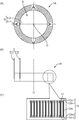
この第1態様の巻線素子用コイル1Aは、中心(軸芯)Oに所定の径を有する円柱状の空芯部Sを設けて、所定の第1厚さを有する長尺な帯状(テープ状、リボン状)の導体部材11を、所定の第2厚さを有する長尺な帯状の絶縁部材12を挟み込みながら所定数パンケーキ状に巻回すことによって成るコイルであり、そして、導体部材11の幅方向(軸方向)の両端も絶縁部材12によって被覆されている。また、導体部材11の長尺方向の両端のそれぞれに第1および第2引出配線5-1、5-2が電気的に導通可能に接続される。ここで、帯状とは、部材の幅Wに対する該部材の厚さtの比t/Wが1より小さくなる矩形断面を有することをいう。幅Wは、長尺方向に直交する幅方向の長さであり、厚さtは、長尺方向に直交するとともに幅方向に直交する厚さ方向の長さでり、フラットワイズ型コイルを形成した場合に、前記部材の幅Wは、軸方向の長さとなり、前記部材の厚さtは、径方向の長さとなる。
より具体的には、前記絶縁部材12は、図3に示すように、導体部材11における前記軸方向に沿う一方面全面を被覆する一方面被覆部12aと、導体部材11における軸方向の両端面全面をそれぞれ被覆する一対の第1および第2端面被覆部12b-1、12b-2と、導体部材11における一方面に対向する他方面の一部を被覆する一対の第1および第2他方面被覆部12c-1、12c-2とを備え、一方面被覆部12aにおける前記軸方向の一方端が第1端面被覆部12b-1を介して第1他方面被覆部12c-1に接続されるとともに一方面被覆部における前記軸方向の他方端が第2端面被覆部12b-2を介して第2他方面被覆部12c-2に接続される.言い換えれば、前記絶縁部材12は、図3に示すように、導体部材11の一方側面全面を被覆する一方面被覆部12aと、一方面被覆部12aにおける幅方向の両端から延長され、導体部材11の幅方向の両端を被覆する一対の第1および第2端部被覆部12b-1、12b-2と、一対の第1および第2端部被覆部12b-1、12b-2のそれぞれから延長され、導体部材11における前記一方側面に対向する他方側面の一部を被覆する一対の第1および第2他方面被覆部12c-1、12c-2とを備える。なお、図3に示す例では、一対の第1および第2他方面被覆部12c-1、12c-2によって、導体部材11の他方側面の一部が被覆されているが、一対の第1および第2他方面被覆部12c-1、12c-2における各端が重ならずに互いに当接することによって、導体部材11の他方側面全面が被覆されてもよい。
このような絶縁部材12の一方面被覆部12aと一対の第1および第2端部被覆部12b-1、12b-2と一対の第1および第2他方面被覆部12c-1、12c-2によって被覆された導体部材11は、例えば、次のように作成される。図4において、まず、導体部材11が該導体部材11の幅よりも長い幅を持つ長尺な帯状の絶縁部材12と重ねられ、これによって一方面被覆部12aが形成される。続いて、絶縁部材12における幅方向の両側部12d-1、12d-2を折り返すことによって、導体部材11における幅方向の両端面および他方面における幅方向の両側部が、前記絶縁部材12における幅方向の両側部12d-1、12d-2で被覆され、これによって一対の第1および第2端部被覆部12b-1、12b-2ならびに一対の第1および第2他方面被覆部12c-1、12c-2が形成される。図4に示す例では、このように1枚の長尺な帯状の絶縁部材12から、一方面被覆部12a、一対の第1および第2端部被覆部12b-1、12b-2ならびに一対の第1および第2他方面被覆部12c-1、12c-2が形成されている。導体部材11には、例えば、銅等の金属(合金を含む)が用いられ、絶縁部材12には、例えば、PEN(ポリエチレンナフタレート)やPPS(ポリフェニレンサルファイド)等の耐熱性を有した樹脂が用いられる。
そして、第1態様の巻線素子用コイル1Aは、例えば、上述の第1および第2コア部材3、4の各内面によって形成された空間内に収容され、これによって第1実施形態のリアクトルDAが構成される。
なお、導体部材11の厚みをいわゆる表皮厚みδより厚くすると、導体部材11内部に発生する渦電流損が増加することになるので、渦電流を低減する観点から、導体部材11の厚さtは、表皮厚みδ以下であることが好ましい。以下の実施形態も同様である。この表皮厚みδは、角周波数をωとし、透磁率をμとし、電気伝導率をσとする場合に、次式によって与えられる。
δ=(2/ωμσ)1/2
このような第1態様の巻線素子用コイル1Aおよびこれを用いた第1実施形態のリアクトルDAでは、導体部材11における幅方向の両端が、一対の第1および第2端部被覆部12b-1、12b-2で被覆されているので、帯状の導体部材11を巻回した場合に互いに隣接する層間における端部での絶縁が実現される。そして、帯状の導体部材11を巻回した場合に互いに隣接する層間の厚さは、一方面被覆部12aと他方面被覆部12cとの絶縁部材2層分の厚さとなり、前記層間の厚さは、従来に較べて半分に低減される。
また、このような第1態様の巻線素子用コイル1Aを用いた第1実施形態のリアクトルDAでは、導体部材11における幅方向の両端が、一対の第1および第2端部被覆部12b-1、12b-2で被覆されているので、巻線素子用コイル1Aにおける幅方向の一方端と第1コア部材3の円板部3a(第2コア部材4の円板部4a)との間の絶縁、および、巻線素子用コイル1Aにおける幅方向の他方端と第2コア部材4の円板部4a(第1コア部材3の円板部3a)との間の絶縁がより確実に実現される。
なお、第1コア部材3の円板部3a(第2コア部材4の円板部4a)は、上部コア部材の一例に対応し、第2コア部材4の円板部4a(第1コア部材3の円板部3a)は、下部コア部材の一例に対応する。また、図1に示す例では、コア部2は、円筒部3b、4bをさらに備えており、図1に示すリアクトルDは、巻線素子用コイル1Aをコア部2内に収納する、いわゆるポット型のリアクトルである。言い換えれば、ポット型のリアクトルDは、巻線素子用コイル1における軸方向の両端を覆う一対の上部コア部材および下部コア部材と、前記一対の上部コア部材および下部コア部材をこれらの外周縁部で互いに連結する筒状の外周コア部材を備えるコア部内に、巻線素子用コイル1を収納するものである。上述の構成は、このようなポット型のリアクトルDに対し好適である。
(第2態様の巻線素子用コイル)
図5は、図1に示すリアクトルに用いられる、第2態様の巻線素子用コイルの構成を示す図である。図5(A)は、巻線素子用コイルの上面図であり、図5(B)は、巻線素子用コイルの側面図であり、そして、図5(C)は、図5(B)に破線の円形で示す箇所における一部断面拡大図である。
図5は、図1に示すリアクトルに用いられる、第2態様の巻線素子用コイルの構成を示す図である。図5(A)は、巻線素子用コイルの上面図であり、図5(B)は、巻線素子用コイルの側面図であり、そして、図5(C)は、図5(B)に破線の円形で示す箇所における一部断面拡大図である。
第2態様の巻線素子用コイル1Bは、絶縁部材12を伴って巻回されている導体部材11(導体部材11および絶縁部材12の全体)を包む第2絶縁部材13をさらに備えている。より具体的には、この巻線素子用コイル1Bは、例えば、図5に示すように、絶縁部材12の一方面被覆部12aと一対の第1および第2端部被覆部12b-1、12b-2と一対の第1および第2他方面被覆部12c-1、12c-2によって被覆された導体部材11を、その幅方向がコイル1Bの軸方向に沿うように巻回すことによって形成された環状体(リング状体、ドーナツ形状体)を、例えばシート状の第2絶縁部材13でさらに包み込むことによって形成される。言い換えれば、この巻線素子用コイル1Bは、第1態様の巻線素子用コイル1Aを、例えばシート状の第2絶縁部材13でさらに包み込むことによって形成される。前記環状体(第1実施形態の巻線素子用コイル1A)を包み込むことによって、前記シート状の第2絶縁部材13は、管状(チューブ状)となる。第2絶縁部材13には、第1絶縁部材12と同様に、例えば、PENやPPS等の耐熱性を有した樹脂が用いられる。
そして、第2態様の巻線素子用コイル1Bは、例えば、上述の第1および第2コア部材3、4の各内面によって形成された空間内に収容され、これによって第2実施形態のリアクトルDBが構成される。
このような第2態様の巻線素子用コイル1Bおよびこれを用いた第2実施形態のリアクトルDBは、上述の第1態様の巻線素子用コイル1Aおよびこれを用いた第1実施形態のリアクトルDAの作用効果に加えて、第2絶縁部材13をさらに備えることによって、巻線素子用コイル1Bとコア部2との間における絶縁がより確実に実現され、絶縁耐圧をより向上することができる。
(第3態様の巻線素子用コイル)
図6は、図1に示すリアクトルに用いられる、第3態様の巻線素子用コイルの構成を示す図である。図6(A)は、巻線素子用コイルの側面図であり、そして、図6(B)は、図5(A)に破線の円形で示す箇所における一部断面拡大図である。
図6は、図1に示すリアクトルに用いられる、第3態様の巻線素子用コイルの構成を示す図である。図6(A)は、巻線素子用コイルの側面図であり、そして、図6(B)は、図5(A)に破線の円形で示す箇所における一部断面拡大図である。
第3態様の巻線素子用コイル1Cは、絶縁部材12を伴って巻回されている導体部材11における軸方向(幅方向)の両端を覆う第3絶縁部材14(14-1、14-2)をさらに備えている。言い換えれば、第3態様の巻線素子用コイル1Cは、絶縁部材12の第1端面被覆部12b-1上を覆う上部絶縁部材14-1および絶縁部材12の第2端面被覆部12b-2上を覆う下部絶縁部材14-2をさらに備えている。より具体的には、第3絶縁部材14は、例えば、図6に示すように、絶縁部材12の一方面被覆部12aと一対の第1および第2端部被覆部12b-1、12b-2と一対の第1および第2他方面被覆部12c-1、12c-2によって被覆された導体部材11を、その幅方向が巻線素子用コイル1Cの軸方向に沿うように巻回すことによって形成された環状体における軸方向の一方端の端面を被覆する環状板体である上部絶縁部材14-1と、前記環状体における軸方向の他方端の端面を被覆する環状板体である下部絶縁部材14-2とを備えている。すなわち、この巻線素子用コイル1Cは、第1態様の巻線素子用コイル1Aにおける軸方向の一方端の端面(上端面)が環状板体の上部絶縁部材14-1によって被覆されるともに、第1態様の巻線素子用コイル1Aにおける軸方向の他方端の端面(下端面)が環状板体の下部絶縁部材14-2によって被覆される。このような第3絶縁部材14には、第1および第2絶縁部材12、13と同様に、例えば、PENやPPS等の耐熱性を有した樹脂が用いられる。
図6に示す例では、上部絶縁部材14-1は、その環状板体の内周縁および外周縁のそれぞれから延長されて垂設された短高の内周円筒部および外周円筒部を備えており、下部絶縁部材14-2は、その環状板体の内周縁および外周縁のそれぞれから延長されて垂設された短高の内周円筒部および外周円筒部を備えている。
そして、第3態様の巻線素子用コイル1Cは、例えば、上述の第1および第2コア部材3、4の各内面によって形成された空間内に収容され、これによって第3実施形態のリアクトルDCが構成される。
このような第3態様の巻線素子用コイル1Cおよびこれを用いた第3実施形態のリアクトルDCは、第1態様の巻線素子用コイル1Aおよびこれを用いた第1実施形態のリアクトルDAの作用効果に加えて、第3絶縁部材14をさらに備えることによって、前記両端での巻線素子用コイル1Cとコア部2との間における絶縁がより確実に実現され、絶縁耐力をより向上することができる。
なお、上述において、第3態様の巻線素子用コイル1Cは、より確実に絶縁して絶縁耐力を向上するために、絶縁部材12を伴って巻回されている導体部材11の最内周内側周側面を被覆する第4絶縁部材(不図示)をさらに備えてもよく、さらに、絶縁部材12を伴って巻回されている導体部材11の最外周外側周側面を被覆する第5絶縁部材(不図示)をさらに備えてもよい。
(リアクトルの製造方法)
次に、これら第1ないし第3態様の巻線素子用コイル1A、1B、1Cを用いた第1ないし第3実施形態のリアクトルDA、DB、DCの製造方法について説明する。ここでは、第1態様の巻線素子用コイル1Aを用いた第1実施形態のリアクトルDAを製造するための製造方法について説明するが、第1態様の巻線素子用コイル1Aに代え、第2態様の巻線素子用コイル1Bを用いることによって、同様に、第2実施形態のリアクトルDBを製造することができ、また、第1態様の巻線素子用コイル1Aに代え、第3態様の巻線素子用コイル1Cを用いることによって、同様に、第3実施形態のリアクトルDCを製造することができる。
次に、これら第1ないし第3態様の巻線素子用コイル1A、1B、1Cを用いた第1ないし第3実施形態のリアクトルDA、DB、DCの製造方法について説明する。ここでは、第1態様の巻線素子用コイル1Aを用いた第1実施形態のリアクトルDAを製造するための製造方法について説明するが、第1態様の巻線素子用コイル1Aに代え、第2態様の巻線素子用コイル1Bを用いることによって、同様に、第2実施形態のリアクトルDBを製造することができ、また、第1態様の巻線素子用コイル1Aに代え、第3態様の巻線素子用コイル1Cを用いることによって、同様に、第3実施形態のリアクトルDCを製造することができる。
図7は、図1に示す第1実施形態におけるリアクトルを製造するための製造方法を示す図である。図7において、まず、図7(A)に示すように、長尺な帯状の導体部材11が該導体部材11の幅よりも長い(広い)幅を持つ長尺な帯状の絶縁部材12上に重ねられる。続いて、図7(B)に示すように、絶縁部材12における幅方向の両側部12d-1、12d-2を折り返すことによって導体部材11における幅方向の両端および他方面における幅方向の両側部が絶縁部材12における幅方向の両側部で被覆される。
続いて、図7(C)に示すように、この絶縁部材12を伴う導体部材11が、中心(軸芯)Oから所定の径だけ離間した位置から所定回数だけ巻き回される。これにより、中心に所定の径を有する円柱状の空芯部Sを備えたパンケーキ構造の巻線素子用コイル1Aが形成される。
続いて、図7(D)に示すように、第1および第2コア部材3、4が、巻線素子用コイル1Aを挟み込むように各円筒部3b、4bの端面同士で重ね合わされる。これにより、図7(E)に示すような例えば円板状のリアクトルDAが生成される。
次に、実施例および比較例について説明する。
(実施例および比較例)
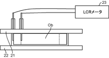
図8は、Q値を測定するための測定系を示す図である。図9は、絶縁耐圧試験を行うための測定系を示す図である。
図8は、Q値を測定するための測定系を示す図である。図9は、絶縁耐圧試験を行うための測定系を示す図である。

表1に示すように、実施例1ないし実施例6(試料No.3~8)、比較例1(試料No.1)および比較例2(試料No.2)における各巻線素子用コイルは、導体部材および巻数が共通であって、絶縁部材および第2絶縁部材の有無が異なっている。共通に用いられる導体部材は、幅20mmで厚さ0.3mmの純銅であり、共通な巻数は、30ターンである。
実施例1ないし実施例3(試料No.3ないし試料No.5)の巻線素子用コイルは、第1態様の巻線素子用コイル1Aを具体的に構成したものである。実施例1(試料No.3)では、絶縁部材12は、幅26mmで厚さ0.025mmの樹脂テープ(PENテープ)であり、折り返しの第1および第2他方面被覆部12c-1、12c-2のそれぞれは、長さ3mmである。実施例2(試料No.4)では、絶縁部材12は、幅30mmで厚さ0.025mmの樹脂テープ(PENテープ)であり、折り返しの第1および第2他方面被覆部12c-1、12c-2のそれぞれは、長さ5mmである。実施例3(試料No.5)では、絶縁部材12は、幅34mmで厚さ0.025mmの樹脂テープ(PENテープ)であり、折り返しの第1および第2他方面被覆部12c-1、12c-2のそれぞれは、長さ7mmである。
また、実施例4ないし実施例6(試料No.6ないし試料No.8)のリアクトルは、第2態様の巻線素子用コイル1Bを具体的に構成したものである。第2絶縁部材13は、実施例4ないし実施例6において共通であり、厚さ0.05mmの絶縁フィルムである。実施例4(試料No.6)では、絶縁部材12は、幅26mmで厚さ0.025mmの樹脂テープ(PENテープ)であり、折り返しの第1および第2他方面被覆部12c-1、12c-2のそれぞれは、長さ3mmである。実施例5(試料No.7)では、絶縁部材12は、幅30mmで厚さ0.025mmの樹脂テープ(PENテープ)であり、折り返しの第1および第2他方面被覆部12c-1、12c-2のそれぞれは、長さ5mmである。実施例6(試料No.8)では、絶縁部材12は、幅34mmで厚さ0.025mmの樹脂テープ(PENテープ)であり、折り返しの第1および第2他方面被覆部12c-1、12c-2のそれぞれは、長さ7mmである。
これらに対し、比較例1(試料No.1)および比較例2(試料No.2)の各巻線素子用コイルは、上述の第1および第2端部被覆部12b-1、12b-2および第1および第2他方面被覆部12c-1、12c-2に相当する絶縁部材が無く、単純に導体部材と絶縁部材とを重ねて巻回したコイルを用いたものである。比較例1(試料No.1)のコイルは、例えば特許文献2に開示のパンケーキ形コイルに対応する。そして、比較例2(試料No.2)は、このようなコイル全体をさらに絶縁フィルムで包み込んだものである。比較例1(試料No.1)では、絶縁部材は、幅20mmで厚さ0.025mmの樹脂テープ(PENテープ)である。比較例2(試料No.2)では、絶縁部材は、幅20mmで厚さ0.025mmの樹脂テープ(PENテープ)であり、コイル全体を包み込む前記絶縁フィルムは、厚さ0.05mmである。
これら実施例1ないし実施例6、比較例1および比較例2の各リアクトルに対し、Q値の測定および絶縁耐圧試験が行われた。Q値は、交流損失(渦電流損)を反映する指標であり、Q値が高い方(大きい方)が交流損失(渦電流損)は、小さい。このため、Q値は、大きい方が効率が高く望ましい。
Q値の測定では、図8に示すように、円板状の上下一対のコア部材間に、測定対象のコイルObが挟み込まれ、測定対象のコイルObの引出配線にLCRメータ23が接続された。このような測定系において、測定対象のコイルObに電圧1Vの周波数10kHz~20kHzである交流電力が給電され、LCRメータ23によってQ値が測定された。
また、絶縁耐圧試験では、図9に示すように、例えばアルミニウム製の導体板31上に、測定対象のコイルObが載置され、測定対象のコイルObにおける一方の引出配線に交流電源32が接続された。このような測定系において、測定対象のコイルObに商用周波数50Hzの交流電力が給電され、1分間で0Vから2.0kVまで昇圧することによって絶縁耐圧が試験された。絶縁耐圧の評価は、昇圧後、2.0kVを印加した状態で、1分間、漏れ電流0.5mA未満である場合に、合格と判定され、一方、昇圧開始後に、0.5mA以上の漏れ電流が流れた場合に、不合格と判定される。この0.5mA以上の漏れ電流が流れた時点の印加電圧が耐電圧とされる。
このようなQ値の測定結果および絶縁耐圧試験が1つの測定対象のコイルObに対し、複数回実行され、Q値は、その平均値とされた。これらの結果は、上記表1に示す通りである。
絶縁耐圧試験では、実施例1ないし実施例6および比較例2は、耐電圧が2.0kV以上であって、絶縁耐圧試験に合格であったが、比較例1は、耐電圧が0.96~1.11kV程度であって、絶縁耐圧試験に不合格であった。
また、Q値の測定では、実施例1の測定値(平均のQ値)を100とした場合に、実施例2のQ値は、107であり、実施例3のQ値は、105であり、実施例4のQ値は、98であり、実施例5のQ値は、101であり、そして、実施例6のQ値は、103であった。一方、比較例1のQ値は、13であり(測定結果範囲2ないし35の平均値)、そして、比較例2のQ値は、17であった(測定結果範囲3ないし45の平均値)。この結果、比較例1および比較例2では、交流電力を給電すると、測定対象のコイルObの各層間で電流が漏れ流れる漏れ電流の存在(これを微短絡と称する)により、コイルObで発生する渦電流損の増大が推測され、このため、Q値が低いものとなったと、本件発明者は、推察している。これに対し、実施例1ないし実施例6は、このような微短絡が無いと推察され、Q値は、良好であった。
本明細書は、上記のように様々な態様の技術を開示しているが、そのうち主な技術を以下に纏める。
一態様にかかる巻線素子用コイルは、長尺な帯状の導体部材と、前記導体部材の一方側面全面を被覆する一方面被覆部と、前記一方面被覆部における幅方向の両端から延長され、前記導体部材の幅方向の両端をそれぞれ被覆する一対の第1および第2端部被覆部と、前記一対の第1および第2端部被覆部のそれぞれから延長され、前記導体部材における前記一方側面に対向する他方側面の一部を被覆する一対の第1および第2他方面被覆部とを備える絶縁部材とを備え、前記絶縁部材の前記一方面被覆部と前記一対の第1および第2端部被覆部と前記一対の第1および第2他方面被覆部によって被覆された前記導体部材は、前記幅方向がコイルの軸方向に沿うように巻回されている。そして、好ましくは、この巻線素子用コイルにおいて、前記絶縁部材は、前記導体部材の幅よりも長い幅を持つ長尺な帯状の部材であり、前記導体部材は、前記絶縁部材と重ねられているとともに、前記絶縁部材における幅方向の両側部を折り返すことによって、幅方向の両端が前記絶縁部材における幅方向の両側部で被覆されて、前記幅方向がコイルの軸方向に沿うように巻回されている。そして、他の一態様にかかる巻線素子用コイルは、コイル状に巻回された、軸方向の幅が径方向の厚さよりも長い導体部材と、前記導体部材における前記軸方向に沿う一方面全面を被覆する一方面被覆部と、前記導体部材における軸方向の両端面全面をそれぞれ被覆する一対の第1および第2端面被覆部と、前記導体部材における前記一方面に対向する他方面の一部を被覆する一対の第1および第2他方面被覆部とを備え、前記一方面被覆部における前記軸方向の一方端が前記第1端面被覆部を介して前記第1他方面被覆部に接続され、前記一方面被覆部における前記軸方向の他方端が前記第2端面被覆部を介して前記第2他方面被覆部に接続されている絶縁部材とを備える。そして、好ましくは、この巻線素子用コイルにおいて、前記絶縁部材は、前記導体部材と重ねられ、前記導体部材における軸方向の幅よりも長い幅を持つ長尺の帯状の部材であって、前記絶縁部材における前記導体部材との重なり部分が前記一方面被覆部であり、前記絶縁部材における幅方向の両側の各折り返し部分がそれぞれ前記第1端面被覆部および前記第1他方面被覆部と前記第2端面被覆部および第2他方面被覆部とである。
このような巻線素子用コイルでは、導体部材における幅方向の両端は、一対の第1および第2端部被覆部で被覆されているので、帯状の導体部材を巻回した場合に互いに隣接する層間における端部での絶縁が実現される。そして、帯状の導体部材を巻回した場合に互いに隣接する層間の厚さは、一方面被覆部と他方面被覆部との絶縁部材2層分の厚さとなり、前記層間の厚さは、従来に較べて半分に低減される。
また、他の一態様では、上述の巻線素子用コイルにおいて、前記導体部材および前記絶縁部材の全体を包む第2絶縁部材をさらに備える。
このような巻線素子用コイルでは、前記導体部材および前記絶縁部材の全体が第2絶縁部材によって包まれるので、外部との間の絶縁がより確実に実現される。
また、他の一態様では、上述の巻線素子用コイルにおいて、前記絶縁部材の前記第1端面被覆部上を覆う上部絶縁部材および前記絶縁部材の前記第2端面被覆部上を覆う下部絶縁部材をさらに備える。
このような巻線素子用コイルでは、前記巻回された導体部材における軸方向の両端面が上部絶縁部材および下部絶縁部材によってそれぞれ覆われるので、前記両端面での外部との間の絶縁がより確実に実現される。
また、他の一態様にかかる巻線素子は、これら上述のいずれかの巻線素子用コイルと、前記巻線素子用コイルによって生じた磁束を通すコア部とを備える。
このような巻線素子では、前記導体部材における幅方向の両側部は、折り返された前記絶縁部材における幅方向の両側部で被覆されているので、帯状の導体部材を巻回した場合に互いに隣接する層間における端部での絶縁が実現される。そして、前記絶縁部材における幅方向の両側部が折り返されるだけであるので、帯状の導体部材を巻回した場合に互いに隣接する層間の厚さは、絶縁部材2層分の厚さとなり、前記層間の厚さは、従来に較べて半分に低減される。
また、他の一態様では、上述の巻線素子において、前記コア部は、前記巻線素子用コイルにおける軸方向の両端を覆う一対の上部コア部材および下部コア部材を備える。
このような巻線素子では、前記巻回された導体部材における幅方向の一方端と前記上部コア部材との間の絶縁、および、前記巻回された導体部材における幅方向の他方端と前記下部コア部材との間の絶縁がより確実に実現される。
この出願は、2011年10月14日に出願された日本国特許出願特願2011-226469を基礎とするものであり、その内容は、本願に含まれるものである。
本発明を表現するために、上述において図面を参照しながら実施形態を通して本発明を適切且つ十分に説明したが、当業者であれば上述の実施形態を変更および/または改良することは容易に為し得ることであると認識すべきである。したがって、当業者が実施する変更形態または改良形態が、請求の範囲に記載された請求項の権利範囲を離脱するレベルのものでない限り、当該変更形態または当該改良形態は、当該請求項の権利範囲に包括されると解釈される。
本発明によれば、巻線素子用コイルおよび巻線素子を提供することができる。
Claims (10)
- コイル状に巻回された、軸方向の幅が径方向の厚さよりも長い導体部材と、
前記導体部材における前記軸方向に沿う一方面全面を被覆する一方面被覆部と、前記導体部材における軸方向の両端面全面をそれぞれ被覆する一対の第1および第2端面被覆部と、前記導体部材における前記一方面に対向する他方面の一部を被覆する一対の第1および第2他方面被覆部とを備え、前記一方面被覆部における前記軸方向の一方端が前記第1端面被覆部を介して前記第1他方面被覆部に接続され、前記一方面被覆部における前記軸方向の他方端が前記第2端面被覆部を介して前記第2他方面被覆部に接続されている絶縁部材とを備えること
を特徴とする巻線素子用コイル。 - 前記絶縁部材は、前記導体部材と重ねられ、前記導体部材における軸方向の幅よりも長い幅を持つ長尺の帯状の部材であって、
前記絶縁部材における前記導体部材との重なり部分が前記一方面被覆部であり、前記絶縁部材における幅方向の両側の各折り返し部分がそれぞれ前記第1端面被覆部および前記第1他方面被覆部と前記第2端面被覆部および第2他方面被覆部とであること
を特徴とする請求項1に記載の巻線素子用コイル。 - 前記導体部材および前記絶縁部材の全体を包む第2絶縁部材をさらに備えること
を特徴とする請求項1に記載の巻線素子用コイル。 - 前記導体部材および前記絶縁部材の全体を包む第2絶縁部材をさらに備えること
を特徴とする請求項2に記載の巻線素子用コイル。 - 前記絶縁部材の前記第1端面被覆部上を覆う上部絶縁部材および前記絶縁部材の前記第2端面被覆部上を覆う下部絶縁部材をさらに備えること
を特徴とする請求項1に記載の巻線素子用コイル。 - 前記絶縁部材の前記第1端面被覆部上を覆う上部絶縁部材および前記絶縁部材の前記第2端面被覆部上を覆う下部絶縁部材をさらに備えること
を特徴とする請求項2に記載の巻線素子用コイル。 - 請求項1に記載の巻線素子用コイルと、
前記巻線素子用コイルによって生じた磁束を通すコア部とを備えること
を特徴とする巻線素子。 - 請求項2に記載の巻線素子用コイルと、
前記巻線素子用コイルによって生じた磁束を通すコア部とを備えること
を特徴とする巻線素子。 - 前記コア部は、前記巻線素子用コイルにおける軸方向の両端を覆う一対の上部コア部材および下部コア部材を備えること
を特徴とする請求項7に記載の巻線素子。 - 前記コア部は、前記巻線素子用コイルにおける軸方向の両端を覆う一対の上部コア部材および下部コア部材を備えること
を特徴とする請求項8に記載の巻線素子。
Applications Claiming Priority (2)
| Application Number | Priority Date | Filing Date | Title |
|---|---|---|---|
| JP2011226469A JP2013089656A (ja) | 2011-10-14 | 2011-10-14 | 巻線素子用コイルおよび巻線素子 |
| JP2011-226469 | 2011-10-14 |
Publications (1)
| Publication Number | Publication Date |
|---|---|
| WO2013054473A1 true WO2013054473A1 (ja) | 2013-04-18 |
Family
ID=48081544
Family Applications (1)
| Application Number | Title | Priority Date | Filing Date |
|---|---|---|---|
| PCT/JP2012/005953 Ceased WO2013054473A1 (ja) | 2011-10-14 | 2012-09-19 | 巻線素子用コイルおよび巻線素子 |
Country Status (2)
| Country | Link |
|---|---|
| JP (1) | JP2013089656A (ja) |
| WO (1) | WO2013054473A1 (ja) |
Families Citing this family (2)
| Publication number | Priority date | Publication date | Assignee | Title |
|---|---|---|---|---|
| JP6235452B2 (ja) * | 2014-12-17 | 2017-11-22 | 株式会社神戸製鋼所 | リアクトル |
| JP6317244B2 (ja) * | 2014-12-17 | 2018-04-25 | 株式会社神戸製鋼所 | 誘導加熱用コイルユニットおよび誘導加熱装置 |
Citations (2)
| Publication number | Priority date | Publication date | Assignee | Title |
|---|---|---|---|---|
| JPH11154619A (ja) * | 1997-11-21 | 1999-06-08 | Matsushita Electric Ind Co Ltd | 溶接電源用トランス |
| JP2011082489A (ja) * | 2009-07-16 | 2011-04-21 | Kobe Steel Ltd | リアクトル |
Family Cites Families (2)
| Publication number | Priority date | Publication date | Assignee | Title |
|---|---|---|---|---|
| JPS5811814U (ja) * | 1981-07-10 | 1983-01-25 | 昭和電線電纜株式会社 | 平角絶縁電線 |
| JPH08153631A (ja) * | 1991-12-25 | 1996-06-11 | Kyoei Denki Kk | トランス |
-
2011
- 2011-10-14 JP JP2011226469A patent/JP2013089656A/ja active Pending
-
2012
- 2012-09-19 WO PCT/JP2012/005953 patent/WO2013054473A1/ja not_active Ceased
Patent Citations (2)
| Publication number | Priority date | Publication date | Assignee | Title |
|---|---|---|---|---|
| JPH11154619A (ja) * | 1997-11-21 | 1999-06-08 | Matsushita Electric Ind Co Ltd | 溶接電源用トランス |
| JP2011082489A (ja) * | 2009-07-16 | 2011-04-21 | Kobe Steel Ltd | リアクトル |
Also Published As
| Publication number | Publication date |
|---|---|
| JP2013089656A (ja) | 2013-05-13 |
Similar Documents
| Publication | Publication Date | Title |
|---|---|---|
| JP5307105B2 (ja) | 複合型巻線素子ならびにこれを用いた変圧器、変圧システムおよびノイズカットフィルタ用複合型巻線素子 | |
| US8614617B2 (en) | Reactor | |
| US20090302986A1 (en) | Minimal-length windings for reduction of copper power losses in magnetic elements | |
| JP4997330B2 (ja) | 多相変圧器および変圧システム | |
| JP5413445B2 (ja) | トランス | |
| JP6056100B2 (ja) | 渦巻型コイル | |
| US9330834B2 (en) | Reactor | |
| JP3144913B2 (ja) | 薄型トランス及びそれを用いた電源装置 | |
| JP6205302B2 (ja) | ノイズ低減用巻線素子およびインバータ装置 | |
| JP6539024B2 (ja) | コイル、及びコイル部品 | |
| JP6113952B2 (ja) | リアクトルおよびこれを用いたノイズフィルター | |
| JP2009164012A (ja) | 誘導加熱コイル | |
| JP5218772B2 (ja) | リアクトル、リアクトル用コイル、及びコンバータ | |
| WO2013054473A1 (ja) | 巻線素子用コイルおよび巻線素子 | |
| JPH1116751A (ja) | トランス | |
| CN210325464U (zh) | 磁感线圈 | |
| CN107527730A (zh) | 一种线圈组件及使用该线圈组件的电器设备及其制造方法 | |
| CN119993705A (zh) | 磁器件及其制备方法、功率转换装置 | |
| JP5926060B2 (ja) | 巻線素子 | |
| KR101925216B1 (ko) | 판상 적층형 리액터 장치 및 그 제조 방법 | |
| JP5218773B2 (ja) | リアクトル及びコンバータ | |
| CN112216481A (zh) | 磁感线圈 | |
| JP3192946B2 (ja) | 電力変換装置用空芯リアクトル | |
| KR101938479B1 (ko) | 적층형 경량 리액터 장치 및 그 제조 방법 | |
| JP2012060194A (ja) | 多相変圧器および変圧システム |
Legal Events
| Date | Code | Title | Description |
|---|---|---|---|
| 121 | Ep: the epo has been informed by wipo that ep was designated in this application |
Ref document number: 12840503 Country of ref document: EP Kind code of ref document: A1 |
|
| NENP | Non-entry into the national phase |
Ref country code: DE |
|
| 122 | Ep: pct application non-entry in european phase |
Ref document number: 12840503 Country of ref document: EP Kind code of ref document: A1 |