WO2013048195A2 - 드라이빙 백 현상을 이용한 터치 검출수단, 검출방법 및 터치스크린패널과, 그러한 터치스크린패널을 내장한 표시장치 - Google Patents
드라이빙 백 현상을 이용한 터치 검출수단, 검출방법 및 터치스크린패널과, 그러한 터치스크린패널을 내장한 표시장치 Download PDFInfo
- Publication number
- WO2013048195A2 WO2013048195A2 PCT/KR2012/007940 KR2012007940W WO2013048195A2 WO 2013048195 A2 WO2013048195 A2 WO 2013048195A2 KR 2012007940 W KR2012007940 W KR 2012007940W WO 2013048195 A2 WO2013048195 A2 WO 2013048195A2
- Authority
- WO
- WIPO (PCT)
- Prior art keywords
- touch
- voltage
- common voltage
- driving
- touch pad
- Prior art date
Links
Images


Classifications
-
- G—PHYSICS
- G06—COMPUTING; CALCULATING OR COUNTING
- G06F—ELECTRIC DIGITAL DATA PROCESSING
- G06F3/00—Input arrangements for transferring data to be processed into a form capable of being handled by the computer; Output arrangements for transferring data from processing unit to output unit, e.g. interface arrangements
- G06F3/01—Input arrangements or combined input and output arrangements for interaction between user and computer
- G06F3/03—Arrangements for converting the position or the displacement of a member into a coded form
- G06F3/041—Digitisers, e.g. for touch screens or touch pads, characterised by the transducing means
- G06F3/044—Digitisers, e.g. for touch screens or touch pads, characterised by the transducing means by capacitive means
- G06F3/0443—Digitisers, e.g. for touch screens or touch pads, characterised by the transducing means by capacitive means using a single layer of sensing electrodes
-
- G—PHYSICS
- G06—COMPUTING; CALCULATING OR COUNTING
- G06F—ELECTRIC DIGITAL DATA PROCESSING
- G06F3/00—Input arrangements for transferring data to be processed into a form capable of being handled by the computer; Output arrangements for transferring data from processing unit to output unit, e.g. interface arrangements
- G06F3/01—Input arrangements or combined input and output arrangements for interaction between user and computer
- G06F3/03—Arrangements for converting the position or the displacement of a member into a coded form
- G06F3/033—Pointing devices displaced or positioned by the user, e.g. mice, trackballs, pens or joysticks; Accessories therefor
- G06F3/0354—Pointing devices displaced or positioned by the user, e.g. mice, trackballs, pens or joysticks; Accessories therefor with detection of 2D relative movements between the device, or an operating part thereof, and a plane or surface, e.g. 2D mice, trackballs, pens or pucks
- G06F3/03545—Pens or stylus
-
- G—PHYSICS
- G06—COMPUTING; CALCULATING OR COUNTING
- G06F—ELECTRIC DIGITAL DATA PROCESSING
- G06F3/00—Input arrangements for transferring data to be processed into a form capable of being handled by the computer; Output arrangements for transferring data from processing unit to output unit, e.g. interface arrangements
- G06F3/01—Input arrangements or combined input and output arrangements for interaction between user and computer
- G06F3/03—Arrangements for converting the position or the displacement of a member into a coded form
- G06F3/041—Digitisers, e.g. for touch screens or touch pads, characterised by the transducing means
- G06F3/0416—Control or interface arrangements specially adapted for digitisers
- G06F3/04164—Connections between sensors and controllers, e.g. routing lines between electrodes and connection pads
-
- G—PHYSICS
- G06—COMPUTING; CALCULATING OR COUNTING
- G06F—ELECTRIC DIGITAL DATA PROCESSING
- G06F3/00—Input arrangements for transferring data to be processed into a form capable of being handled by the computer; Output arrangements for transferring data from processing unit to output unit, e.g. interface arrangements
- G06F3/01—Input arrangements or combined input and output arrangements for interaction between user and computer
- G06F3/03—Arrangements for converting the position or the displacement of a member into a coded form
- G06F3/041—Digitisers, e.g. for touch screens or touch pads, characterised by the transducing means
- G06F3/0416—Control or interface arrangements specially adapted for digitisers
- G06F3/0418—Control or interface arrangements specially adapted for digitisers for error correction or compensation, e.g. based on parallax, calibration or alignment
-
- G—PHYSICS
- G06—COMPUTING; CALCULATING OR COUNTING
- G06F—ELECTRIC DIGITAL DATA PROCESSING
- G06F3/00—Input arrangements for transferring data to be processed into a form capable of being handled by the computer; Output arrangements for transferring data from processing unit to output unit, e.g. interface arrangements
- G06F3/01—Input arrangements or combined input and output arrangements for interaction between user and computer
- G06F3/03—Arrangements for converting the position or the displacement of a member into a coded form
- G06F3/041—Digitisers, e.g. for touch screens or touch pads, characterised by the transducing means
- G06F3/044—Digitisers, e.g. for touch screens or touch pads, characterised by the transducing means by capacitive means
- G06F3/0446—Digitisers, e.g. for touch screens or touch pads, characterised by the transducing means by capacitive means using a grid-like structure of electrodes in at least two directions, e.g. using row and column electrodes
-
- G—PHYSICS
- G06—COMPUTING; CALCULATING OR COUNTING
- G06F—ELECTRIC DIGITAL DATA PROCESSING
- G06F3/00—Input arrangements for transferring data to be processed into a form capable of being handled by the computer; Output arrangements for transferring data from processing unit to output unit, e.g. interface arrangements
- G06F3/01—Input arrangements or combined input and output arrangements for interaction between user and computer
- G06F3/03—Arrangements for converting the position or the displacement of a member into a coded form
- G06F3/041—Digitisers, e.g. for touch screens or touch pads, characterised by the transducing means
- G06F3/044—Digitisers, e.g. for touch screens or touch pads, characterised by the transducing means by capacitive means
- G06F3/0448—Details of the electrode shape, e.g. for enhancing the detection of touches, for generating specific electric field shapes, for enhancing display quality
-
- G—PHYSICS
- G09—EDUCATION; CRYPTOGRAPHY; DISPLAY; ADVERTISING; SEALS
- G09G—ARRANGEMENTS OR CIRCUITS FOR CONTROL OF INDICATING DEVICES USING STATIC MEANS TO PRESENT VARIABLE INFORMATION
- G09G3/00—Control arrangements or circuits, of interest only in connection with visual indicators other than cathode-ray tubes
- G09G3/20—Control arrangements or circuits, of interest only in connection with visual indicators other than cathode-ray tubes for presentation of an assembly of a number of characters, e.g. a page, by composing the assembly by combination of individual elements arranged in a matrix no fixed position being assigned to or needed to be assigned to the individual characters or partial characters
- G09G3/34—Control arrangements or circuits, of interest only in connection with visual indicators other than cathode-ray tubes for presentation of an assembly of a number of characters, e.g. a page, by composing the assembly by combination of individual elements arranged in a matrix no fixed position being assigned to or needed to be assigned to the individual characters or partial characters by control of light from an independent source
- G09G3/36—Control arrangements or circuits, of interest only in connection with visual indicators other than cathode-ray tubes for presentation of an assembly of a number of characters, e.g. a page, by composing the assembly by combination of individual elements arranged in a matrix no fixed position being assigned to or needed to be assigned to the individual characters or partial characters by control of light from an independent source using liquid crystals
- G09G3/3611—Control of matrices with row and column drivers
- G09G3/3648—Control of matrices with row and column drivers using an active matrix
- G09G3/3655—Details of drivers for counter electrodes, e.g. common electrodes for pixel capacitors or supplementary storage capacitors
-
- G—PHYSICS
- G09—EDUCATION; CRYPTOGRAPHY; DISPLAY; ADVERTISING; SEALS
- G09G—ARRANGEMENTS OR CIRCUITS FOR CONTROL OF INDICATING DEVICES USING STATIC MEANS TO PRESENT VARIABLE INFORMATION
- G09G3/00—Control arrangements or circuits, of interest only in connection with visual indicators other than cathode-ray tubes
- G09G3/20—Control arrangements or circuits, of interest only in connection with visual indicators other than cathode-ray tubes for presentation of an assembly of a number of characters, e.g. a page, by composing the assembly by combination of individual elements arranged in a matrix no fixed position being assigned to or needed to be assigned to the individual characters or partial characters
- G09G3/34—Control arrangements or circuits, of interest only in connection with visual indicators other than cathode-ray tubes for presentation of an assembly of a number of characters, e.g. a page, by composing the assembly by combination of individual elements arranged in a matrix no fixed position being assigned to or needed to be assigned to the individual characters or partial characters by control of light from an independent source
- G09G3/36—Control arrangements or circuits, of interest only in connection with visual indicators other than cathode-ray tubes for presentation of an assembly of a number of characters, e.g. a page, by composing the assembly by combination of individual elements arranged in a matrix no fixed position being assigned to or needed to be assigned to the individual characters or partial characters by control of light from an independent source using liquid crystals
- G09G3/3611—Control of matrices with row and column drivers
- G09G3/3696—Generation of voltages supplied to electrode drivers
-
- G—PHYSICS
- G06—COMPUTING; CALCULATING OR COUNTING
- G06F—ELECTRIC DIGITAL DATA PROCESSING
- G06F2203/00—Indexing scheme relating to G06F3/00 - G06F3/048
- G06F2203/041—Indexing scheme relating to G06F3/041 - G06F3/045
- G06F2203/04104—Multi-touch detection in digitiser, i.e. details about the simultaneous detection of a plurality of touching locations, e.g. multiple fingers or pen and finger
-
- G—PHYSICS
- G09—EDUCATION; CRYPTOGRAPHY; DISPLAY; ADVERTISING; SEALS
- G09G—ARRANGEMENTS OR CIRCUITS FOR CONTROL OF INDICATING DEVICES USING STATIC MEANS TO PRESENT VARIABLE INFORMATION
- G09G2310/00—Command of the display device
- G09G2310/08—Details of timing specific for flat panels, other than clock recovery
Definitions
- the present invention relates to a means, a method, and an apparatus for detecting a touch input of a finger of a body or a touch input means having similar conductive characteristics. More particularly, the present invention relates to a driving capacitor applied to a driving capacitor connected to a touch detector, and to a touch input. In this case, the present invention relates to touch detection means, a detection method, a touch screen panel for obtaining a touch signal using a driving back phenomenon generated in the touch detector, and a display device having such a touch screen panel.
- a touch screen panel is attached to a display device such as a liquid crystal display (LCD), a plasma display panel (PDP), an organic light emitting diode (OLED), an active matrix organic light emitting diode (AMOLED), or the like.
- a display device such as a liquid crystal display (LCD), a plasma display panel (PDP), an organic light emitting diode (OLED), an active matrix organic light emitting diode (AMOLED), or the like.
- a signal corresponding to a corresponding position is generated when an object such as a finger or a pen is touched.
- Touch screen panels are used in a wide range of applications, such as small portable terminals, industrial terminals, and digital information devices (DIDs).
- the capacitive touch screen panel has a high transmittance, a soft touch can be recognized, and multi-touch and gesture recognition have advantages of expanding the market.
- a transparent conductive film is formed on upper and lower surfaces of a transparent substrate 2 made of plastic, glass, or the like, and a voltage applying metal electrode 4 is formed at each of four corners of the transparent substrate 2.
- the transparent conductive film is formed of a transparent metal such as indium tin oxide (ITO) or antimony tin oxide (ATO).
- the metal electrodes 4 formed at four corners of the transparent conductive film are formed by printing a conductive metal having a low resistivity such as silver (Ag).
- a resistance network is formed around the metal electrodes 4. The resistance network is formed in a linearization pattern in order to transmit control signals evenly over the entire surface of the transparent conductive film.
- a protective film is coated on the transparent conductive film including the metal electrode 4.
- the capacitive touch screen panel when an alternating current voltage of high frequency is applied to the metal electrode 4, the capacitive touch screen panel spreads on the front surface of the transparent substrate 2. At this time, when the transparent conductive film on the upper surface of the transparent substrate 2 is lightly touched by the finger 8 or the conductive touch input means, a certain amount of current is absorbed into the body and the current sensor built in the controller 6 detects a change in the current. The touch points are recognized by calculating the amount of current in each of the four metal electrodes 4.
- the capacitive touch screen panel as shown in FIG. 1 is a method of detecting the magnitude of the micro current, and thus requires an expensive detection device, which increases the price and makes it difficult to multi-touch to recognize a plurality of touches.
- the capacitive touch screen panel as shown in FIG. 2 is mainly used.
- the touch screen panel of FIG. 2 includes a linear touch pad 5a in the horizontal direction, a linear touch pad 5b in the longitudinal direction, and a touch drive IC 7 for analyzing a touch signal.
- the touch screen panel detects the magnitude of the capacitance formed between the linear touch pad 5 and the finger 8, and scans the horizontal touch pad 5a in the horizontal direction and the linear touch pad 5b in the longitudinal direction. By detecting the signal, a plurality of touch points can be recognized.
- the touch screen panel as described above is mounted and used on a display device such as an LCD, a phenomenon in which signal detection is difficult due to noise occurs.
- the LCD uses a common electrode, and in some cases, an AC common voltage Vcom is applied to the common electrode.
- the common voltage Vcom of the common electrode acts as noise when detecting the touch point.
- FIG. 3 shows an embodiment in which a conventional capacitive touch screen panel is installed on an LCD.
- the display device 200 has a structure in which a liquid crystal is sealed between the lower TFT substrate 205 and the upper color filter 215 to form the liquid crystal layer 210.
- the TFT substrate 205 and the color filter 215 are bonded by the sealant 230 at the outer portion thereof.
- a polarizing plate is attached to the upper and lower sides of the liquid crystal panel, and in addition, a BLU (Back Light Unit) is installed.
- BLU Back Light Unit
- a touch screen panel is installed on the display device 200 as shown.
- the touch screen panel has a structure in which the linear touch pad 5 is mounted on the upper surface of the substrate 1.
- a protective panel 3 is attached to the substrate 1 to protect the linear touch pad 5.
- the touch screen panel is attached to an edge portion of the display device 200 through an adhesive member 9 such as a double adhesive tape (DAT), and forms an air gap 9a between the display device 200.
- DAT double adhesive tape
- a capacitance such as Ct is formed between the finger 8 and the linear touch pad 5.
- a capacitance such as Cvcom, is formed between the linear touch pad 5 and the common electrode 220 formed on the lower surface of the color filter 215 of the display device 200, and the pattern is formed on the linear touch pad 5.
- Cp which is an unknown parasitic capacitance due to capacitance coupling or manufacturing process factors, is also working.
- a circuit such as the equivalent circuit of FIG. 4 is configured.
- the conventional touch screen panel detects a touch by detecting a change amount of Ct, and components such as Cvcom and Cp act as noise in detecting Ct.
- components such as Cvcom and Cp act as noise in detecting Ct.
- the common voltage Vcom of the common electrode 220 since the common voltage Vcom of the common electrode 220 alternates by one or a plurality of gate lines as shown in FIG. It acts as a significant noise during touch detection.
- an air gap 9a is disposed between the touch screen panel and the display device 200 as shown in FIG. 3.
- ITO or the like is applied to the lower surface of the touch screen panel 50 to form a shielding layer, and the shielding layer is grounded with the ground signal.
- the air gap 9a increases the thickness of the product and quality deterioration occurs.
- a separate shielding layer and a manufacturing process are required to configure the shielding layer, an increase in manufacturing cost is caused.
- the touch screen panel is embedded in the LCD, it is impossible to form the air gap 9a or the shielding layer, and thus it is impossible to manufacture the touch screen panel in the LCD or the like.
- the present invention is proposed to solve the problems of the conventional touch screen panel as described above, by connecting a driving capacitor to the touch detection unit to apply a driving voltage to one side of the driving capacitor, between the touch input means such as a hand and the touch pad
- a touch capacitance is formed at the touch capacitance, a touch signal is acquired by using a driving back phenomenon in which the magnitude of the voltage detected by the touch detector is different according to the magnitude of the touch capacitance, thereby obtaining noise from the common electrode of the display device.
- Touch detection means using a new driving back phenomenon that minimizes the influence of the parasitic capacitance, and stably acquires the touch signal, and at the same time integrates the touch screen function into a display device such as an LCD; Detection method and touch screen panel, To provide value markets that purpose.
- the touch detection means of the present invention for achieving the above object is added to the upper surface of the display device for detecting that the touch capacitance (Ct) is generated by the approach of the touch input means, such as a finger of the body or a similar conductor.
- a touch detection means comprising: a touch pad forming a touch capacitance (Ct) between the touch input means; A driving capacitor Cdrv having one side connected to the touch pad and a driving voltage applied to the other side for a touch detection; A common voltage detector detecting a common voltage generated by the display device; A driving voltage generator configured to generate a driving voltage in synchronization with the common voltage; And a touch connected to the touch pad to detect a touch signal by using a driving back phenomenon when the touch capacitance Ct is added to the driving capacitor Cdrv according to whether the touch input means is touched. It is configured to include a detection unit.
- the touch detection means of the present invention for achieving the above object, the touch detection is installed in the display device and the touch detection for detecting the generation of the touch capacitance (Ct) by the approach of the touch input means, such as a finger of the body or a similar conductor.
- the touch detection is installed in the display device and the touch detection for detecting the generation of the touch capacitance (Ct) by the approach of the touch input means, such as a finger of the body or a similar conductor.
- Means comprising: a touch pad for forming a touch capacitance (Ct) between the touch input means; A driving capacitor Cdrv having one side connected to the touch pad and a driving voltage applied to the other side for a touch detection; A common voltage detector detecting a common voltage generated in the display device; A driving voltage generator configured to generate a driving voltage in synchronization with the common voltage; And a touch connected to the touch pad to detect a touch signal by using a driving back phenomenon when the touch capacitance Ct is added to the driving capacitor Cdrv according to whether the touch input means is touched. It is configured to include a detection unit.
- the touch pad forms a common electrode capacitance Cvcom between the common electrode of the display device.
- a driving capacitor Cdrv is not connected to the common voltage detector.
- the touch pad is connected to the touch detector or the common voltage detector.
- charging means for applying a precharge voltage to a touch pad connected to the common voltage detector is connected.
- the charging means is a switching device and the output of the switching device connected to the touch pad connected to the common voltage detector is in a high impedance state when the common voltage is detected.
- the common voltage detector input is in a high impedance state.
- the signal output from the common voltage detector is input to a comparator to detect whether the common voltage is a high state or a low state.
- the comparator is input to the comparator a high reference voltage for detecting a high state of the common voltage and / or a low reference voltage for detecting a low state of the common voltage.
- the charging means of the common voltage detector maintains the off state for a predetermined time and detects the common voltage in the off state.
- the charging means 12 of the common voltage detector 15 performs on / off in synchronization with the common voltage.
- At least one touch pad 10 is sequentially used as the touch pad 10 connected to the common voltage detector 15.
- the touch pad connected to the common voltage detector when the touch pad connected to the common voltage detector is connected to the touch detector, another touch pad is connected to the common voltage detector to detect the common voltage.
- the signal of the common voltage detection unit has a means to be output to the outside of the TDI.
- the display device has means for determining whether to output the signal of the common voltage detector to the outside of the TDI.
- a driving voltage is applied to one side of the driving capacitor Vdrv in synchronization with the rising edge or the falling edge of the common voltage.
- the charging means of the touch detector is a switching device.
- the charging means for the touch detection performs on / off in synchronization with the common voltage.
- the driving voltage is applied to one side of the driving capacitor Cdrv in synchronization with the common voltage or the charging time.
- the touch signal is detected after a predetermined time after the driving voltage is applied.
- the driving voltage has a means for determining a starting point of detecting a touch signal after the driving voltage is applied.
- the touch detection means of the present invention for achieving the above object, in the touch detection means for detecting that the touch capacitance (Ct) is generated by the approach of the touch input means, such as a finger of the body or the like conductor, A touch pad forming a touch capacitance Ct between the touch input means; A driving capacitor Cdrv having one side connected to the touch pad and a driving voltage applied to the other side for a touch detection; A driving voltage generator configured to periodically generate a driving voltage according to a set value; And a touch connected to the touch pad to detect a touch signal by using a driving back phenomenon when the touch capacitance Ct is added to the driving capacitor Cdrv according to whether the touch input means is touched. It is configured to include a detection unit.
- the charging means of the touch detector is a switching device.
- the charging means of the touch detector performs on / off in synchronization with the detection period.
- the driving voltage is applied to one side of the driving capacitor Cdrv in synchronization with the charging time.
- the touch signal is detected after a predetermined time after the driving voltage is applied.
- the device has a means for determining a starting point of detecting a touch signal after the driving voltage is applied.
- the driving voltage applied to the other side of the driving capacitor Cdrv is an alternating voltage alternated at a predetermined frequency.
- a means for varying the size of the driving capacitor Cdrv is provided.
- the driving capacitor Cdrv is not connected to the touch detector 14.
- the touch detector 14 may drive the touch pad 10 at a rising time and / or a falling time of a driving voltage applied to the driving capacitor Cdrv. Detecting a backing phenomenon.
- the touch detector 14 may have a magnitude of the voltage detected by the touch detector when the touch capacitance Ct is added due to the touch generation in preparation for the magnitude of the voltage detected by the touch detector when the touch is not generated.
- the touch signal is detected by detecting a driving back that causes a difference.
- the voltage detected by the touch detector 14 when the touch is not generated is determined by Equation 1 below, and when the touch capacitance Ct is added, the voltage detected by the touch detector is Is determined by Equation 2, and the driving back occurs due to a difference between Equation 1 and Equation 2.
- Vh is the high level voltage applied to the driving capacitor
- Vl is the low level voltage applied to the driving capacitor
- Cdrv is the driving capacitance
- Cvcom is the common electrode capacitance
- Cp is the parasitic capacitance
- Ct is the touch capacitance.
- the touch detector 14 detects the touch area of the touch input means with respect to the touch pad 10 corresponding to the size of the driving back.
- the touch detector 14 includes an amplifier 18 for amplifying the detected voltage.
- the sensor signal line 22 which is present on the left and right sides of the sensor signal line 22 connected to the touch pad 10 that is detecting a touch and is not in touch is in a floating state.
- the touch pad 10 except for the sensor signal line 22 connected to the touch pad 10 that is detecting a touch is in a floating state.
- the touch pad 10 which is present on the left and right sides of the sensor signal line 22 connected to the touch pad 10 that is detecting a touch, and the touch pad 10 that is not touched is turned on by the charging means 12 of the touch detector. It has a floating state before it is turned on.
- the touch pad 10 except for the sensor signal line 22 connected to the touch pad 10 that is detecting a touch is in a floating state before the charging means 12 of the touch detector is turned on.
- the touch pad 10 connected to the touch detector 14 is separated from the touch detector 14.
- the touch pad connected to the touch detector within 1 ns to 100 us is separated from the touch detector 14.
- the touch pad separated from the touch detector is reconnected to the touch detector or a predetermined voltage is applied after touch sensing is completed in the touch detector.
- the predetermined voltage is ground GND or a DC voltage of a predetermined magnitude.
- a predetermined voltage is applied to the floating touch non-detected touch pad 10.
- the predetermined voltage is ground GND or a DC voltage of a predetermined magnitude.
- a resistance of a section in which a touch signal line connected to the touch pad 10 is connected to a connection part with a TDI (Touch Drive IC) is included in -100% to + 100%.
- the separation time of the touch pad connected to the touch detector is equally applied to the plurality of touch pads.
- the touch detection means, the detection method and the touch screen panel using the driving back phenomenon of the present invention, and the display device incorporating such a touch screen panel the common voltage level at which the common electrode of the display device alternates at a predetermined frequency
- the state change of the common voltage is detected and the state change point is avoided.
- Noise and coupling phenomenon are obtained by applying a driving voltage through a driving capacitor connected to the touch detection unit, and detecting a driving back from the touch detection unit by the touch capacitance added by the touch input to obtain a touch signal.
- FIG. 1 is a perspective view showing an example of a conventional touch screen panel
- FIG. 2 is a plan view showing another example of a conventional touch screen panel
- FIG. 3 is a cross-sectional view illustrating an example in which the touch screen panel of FIG. 2 is installed on a display device.
- FIG. 4 is an equivalent circuit diagram of detecting touch capacitance in FIG. 3.
- FIG. 5 is a waveform diagram illustrating a common voltage waveform of a liquid crystal display device
- FIG. 7 is a diagram illustrating a principle of detecting a touch input.
- FIG. 8 is a circuit diagram showing the basic structure of a touch detection means according to the present invention.
- 9A and 9B illustrate a correlation between the breakdown voltage of a TDI and a precharge voltage.
- FIG. 10 is a view showing an embodiment of the present invention regarding the configuration of a touch detection unit
- FIG. 11 is a view showing still another embodiment of the present invention regarding the configuration of a touch detection circuit unit
- FIG. 12 is a cross-sectional view showing an example of a touch pad configuration
- FIG. 13 is a sectional view showing another example of the touch pad configuration
- 14A and 14B illustrate embodiments of a gesture using an area.
- 15A-15C illustrate another embodiment of a gesture using an area.
- 16 is a waveform diagram illustrating a process of detecting a touch signal
- FIG. 17 illustrates an embodiment of the present invention related to a common voltage detection circuit.
- FIG. 19 illustrates a detailed embodiment of the present invention with respect to a common voltage detection circuit.
- 20 is a diagram illustrating an embodiment of a method of recovering when a common voltage detection error occurs
- 21 is a flow chart for factory calibration for common voltage component extraction
- FIG. 22 illustrates an embodiment of the present invention relating to a method of detecting a touch signal in synchronization with a common voltage.
- 23 is a diagram showing an example of a common voltage actually detected
- FIG. 24 is a diagram illustrating an embodiment in which the size of Vdrv varies according to register setting.
- 25 is a view showing an embodiment of the present invention related to an embodiment of a touch screen panel.
- 26A to 26C illustrate embodiments of various configurations of a touch pad.
- FIG. 27 is a view illustrating an embodiment of a touch screen panel shown in FIG.
- FIG. 28 illustrates a conventional embodiment in which sensor signal lines are wired up and down the touch pad
- 29 illustrates an embodiment of a differential amplifier used in the present invention.
- FIG 30 illustrates an embodiment in which an ADC converter is connected to an amplifier output.
- 31 is a flowchart showing a factory calibration method
- 32 is a diagram illustrating an embodiment of the present invention for setting an execution region of an RTC.
- 33 is a diagram illustrating an embodiment of detecting a conventional capacitive touch signal
- FIG. 34 is a diagram of a TFT configuration of a transverse electric field mode LCD substrate.
- 35 shows a conventional embodiment of the background configuration of the transverse electric field mode LCD substrate.
- FIG. 36 is a cross-sectional view of the present invention applied to a transverse electric field mode LCD substrate.
- FIG. 37 is a front view of the present invention applied to a transverse electric field mode LCD substrate.
- FIG. 38 illustrates an embodiment of the invention in which the touchpad is used in the background
- FIG. 39 shows an embodiment of the present invention regarding the layout of the sensor signal line 22.
- 40A to 40C illustrate embodiments of the present invention regarding a space charging unit between a touch detector and a sensor signal line.
- 41 illustrates an embodiment of touch detection error by a conductor.
- FIG. 42 is a view showing an embodiment of the present invention regarding the opening of a non-sensing pad.
- FIG 43 is a view showing an embodiment of the present invention regarding the opening of a sensing pad.
- 44A and 44B illustrate embodiments of the present invention in which touch coordinates are extracted based on data detected or calculated by a touch sensor.
- 45 illustrates an embodiment of the present invention for detecting a touch signal and a common voltage with a touch pad.
- FIG. 48 is a diagram showing an embodiment of a register setting applied to a function key
- 49 is a view showing an embodiment of the present invention regarding the structure of a function keypad
- 50 is a view showing a conventional embodiment of the configuration of the edge portion of the touch screen panel
- 51 is a view showing an embodiment of the present invention regarding the configuration of an edge portion of a touch screen panel.
- FIG. 52 illustrates an embodiment of the present invention in which a plurality of TDIs are used.
- FIG. 54 is a cross-sectional view of a display device incorporating a touch screen panel.
- 55 is an exploded perspective view of a display device with a built-in touch screen panel
- the present invention relates to a touch detection means, a detection method and a touch screen panel using a driving back phenomenon, and a display device incorporating such a touch screen panel.
- the driving back phenomenon caused by the difference in the magnitude of the touch capacitance is applied when an alternating driving voltage is applied to the added driving capacitor.
- the touch detection system according to the present invention is a voltage generated by a driving back phenomenon caused by a driving capacitor, a common electrode capacitance, and a parasitic capacitance when a touch is not generated, and a voltage generated by a driving back phenomenon when a touch capacitance is added by a touch generation.
- the display device referred to in the present invention means any one of LCD, PDP and OLED, or any means for displaying other images.
- the LCD requires a common voltage (Vcom) to drive the liquid crystal.
- Vcom common voltage
- a line inversion method in which a common voltage of a common electrode alternates with one or more gate lines is used to reduce current consumption.
- a large LCD uses a dot inversion driving scheme in which a common voltage of a common electrode has a constant DC level.
- a transverse electric field mode LCD a common electrode is formed in a partial region of the LCD TFT substrate to display an image by a line in version or dot in version driving method.
- a back ground is commonly formed in the entire color filter exposed to the outside through the back ITO, and grounded with a ground signal to prevent ESD.
- common electrodes In addition to the electrode to which the common voltage Vcom is applied as described above, all electrodes that are commonly used in the display device are referred to as common electrodes, and the alternating voltage, DC voltage, or unspecified frequency applied to the common electrode of the display device. Alternating voltages will be referred to as common voltages.
- the present invention detects a non-contact touch input of a touch input means having a finger or similar electrical characteristics.
- the non-contact touch input means that the touch input means such as a finger performs touch input while being spaced apart from the touch pad by a predetermined distance from the substrate.
- the touch input means may contact the outer surface of the substrate.
- the touch input means and the touch pad maintain a non-contact state.
- the touch action of a finger on the touchpad may be expressed in terms of access.
- the finger since the finger may be in contact with the outer surface of the substrate, the touch action of the finger against the substrate may be expressed in terms of contact. In this specification, access and contact are used in the same sense as above.
- an amplifier of a signal is a unit function element, and an assembly of amplifiers or signal converters It can be called a signal converter.
- the part may be included in a larger component or part, or may include smaller components and parts.
- ⁇ may have its own CPU.
- capacitance refers to physical size and is used in the same sense as capacitance.
- a capacitor refers to an element having a capacitance of physical size. Capacitance is created by designed values and processes, or indirectly, as it is naturally produced between two parallel signal lines at arbitrary distances. In the present specification, both a capacitor made directly and an indirectly formed capacitor are referred to as capacitors.
- the term "forcing a signal” means that the level of a signal which has already been maintained is changed or connected to a signal in a floating state.
- applying a signal to the on / off control terminal of the switching element is used to mean that the existing low level voltage is changed to the high level, and the floating state without any signal is used. It may also be used to mean that a voltage is applied to turn on / off the switching element to the on / off control terminal of the switching element.
- the driving back phenomenon or the driving back is used in the same sense and abbreviated as "D / B".
- the touch drive IC (Touch Drive IC) is abbreviated as TDI.
- the meaning of detecting the voltage due to the D / B phenomenon and the meaning of detecting the touch signal are equally used.
- a three-terminal switching device generally includes three terminals of an on / off control terminal Cont, an input terminal In, and an output terminal Out.
- the on / off control terminal is a terminal for controlling the on / off of the switching element.
- the three-terminal switching element referred to as a charging means in the present invention is, for example, a relay, a complementary metal oxide semiconductor (CMOS) switch or a PMOS or NMOS, a bipolar junction transistor (BJT), a field effect transistor (FET), Metal Oxide Semiconductor Field Effect Transistors (MOSFETs), Insulated Gate Bipolar Transistors (IGBTs), Thin Film Transistors (TFTs), and OPAMPs, and may be formed by a homogeneous or heterogeneous combination of these.
- CMOS complementary metal oxide semiconductor
- BJT bipolar junction transistor
- FET field effect transistor
- MOSFETs Metal Oxide Semiconductor Field Effect Transistors
- IGBTs Insulated Gate Bipolar Transistors
- TFTs Thin Film Transistors
- OPAMPs OPAMPs
- the relay may also be a four-terminal element.
- the charging means that can be used in the present invention, any device having an input / output terminal on / off by an on / off control terminal may be used regardless of the number of input / output terminals. .
- the CMOS switch is formed by a combination of PMOS and NMOS, and the input and output terminals are interconnected, but the on / off control terminals are present individually connected to the same control signal, or The on / off state is determined separately by connecting to the control signal.
- Relay is a device that outputs voltage or current applied to input terminal without loss when current is applied to control terminal, and BJT is based on voltage higher than Threshold Value of Base.
- TFT is a switching element used in the pixel part of a display device such as LCD or AMOLED, and is composed of a gate terminal as a control terminal, a source terminal as an input terminal, and a drain terminal as an output terminal.
- a voltage having a threshold value greater than the voltage applied to the drain terminal is applied to the gate terminal, the current flows from the input terminal to the output terminal while conducting the current depending on the magnitude of the voltage applied to the gate terminal.
- FIG. 7 Prior to describing a specific embodiment of the present invention, a principle of detecting a touch input in the present invention will be briefly described with reference to FIG. 7.
- the touch pad 10 and the finger 25 are spaced at an interval of “d”, and “A”. Assume that it has an opposite area of. Then, capacitance “C” is formed between the finger 25 and the touch pad 10, as shown in the right equivalent circuit and the equation of FIG. 7.
- the capacitor V The charge can be accumulated in the relationship of Q / C.
- Detect touch when a driving back having a correlation with the magnitude of the capacitance "C” occurs in the sense pattern 10 connected to the touch detector, Detect touch.
- FIG. 8 is a circuit diagram showing the basic structure of the touch detection means according to the present invention.
- the specialized touch detection means according to the present invention the charging means 12, the touch pad 10, the sensor signal line 22, the driving capacitor (Cdrv), the common electrode capacitor (Cvcom) and the touch detector (14) has a basic structure consisting of.
- the charging means 12 supplies a precharge signal to the touch pad 10, and is turned off by a turn off signal applied to an “on / off control terminal” named “Cont” to output an output terminal ( Make 12-1) high impedance.
- the precharge signal is a voltage for charging these capacitors by applying a DC voltage to all capacitors connected to the output terminal 12-1 of the charging means 12 before the touch signal is detected. Therefore, the charging means 12 is a switching device that performs a switching operation according to a control signal supplied to the on / off control terminal, or a linear device such as an OPAMP to supply a signal according to the control signal.
- the touch pad 10 may be supplied to all capacitors connected to the output unit 12-1 of the charging means 12.
- the charging voltage may be a DC voltage including zero volts and an alternating AC voltage such as a square wave, a triangle wave, or a sine wave.
- This charging voltage is related to the voltage used in the touch drive IC (TDI) in which the touch detection system of the present invention is integrated. 9A and 9B will be described as follows.
- the TDI is broken.
- the potential difference due to D / B which will be described later, as in the embodiment of FIGS. 9A to 9B is 3V.
- the voltage of the output unit 12-1 of the charging means 12 is 3V before the D / B occurs as shown in Figure 9a the voltage of the output unit 12-1 of the charging means by the D / B It is 6V, which exceeds the internal voltage of TDI, 5V, so that the TDI 30 is placed in the damage zone.
- an embodiment of the present invention may have a function of controlling a charging voltage for adjusting the magnitude of the maximum voltage at the time of driving back based on the breakdown voltage of the TDI.
- FIG. 10 is an embodiment of the configuration of the touch detection unit 14 according to the present invention.
- all of the capacitors connected to the output unit 12-1 and the output unit 12-1 of the charging unit 12 are connected to the touch detector 10. Since the D / B phenomenon, which will be described later, occurs in a capacitor connected to the output unit 12-1 of the charging unit 12, the voltage generated by the D / B is transferred to the buffer 14-1 of the touch detector 14. do. Since the input terminal of the buffer 14-1 is generally high impedance (hereinafter referred to as Hi-z), the output unit 12-1 of the charging unit is in the Hi-z state when the output unit 12-1 of the charging unit is in the Hi-z state. ) And all capacitors connected between Buffer 14-1 are also in the Hi-z state.
- the output unit 12-1 of the charging means is directly connected to the buffer 14-1.
- an input such as a gate of a MOS or a gate of a TFT is Hi-z. It can be connected to the terminals of all devices in the state.
- the reason for making the output unit 12-1 and the touch detector 14 of the charging means into the Hi-z state is that the detection time can be lengthened only when the D / B phenomenon described later is detected in the Hi-z state. to be. That is, in the Hi-z state, since there is no discharge path of the isolated charge, the level of the voltage formed by the D / B is maintained for a long time with minimal deformation.
- the signal output from the buffer 14-1 is input to the amplifier 14-2. If the input terminal of the amplifier 4-2 is Hi-z, the point P of FIG. 10 may be directly connected to the input terminal of the amplifier 14-2.
- the P point signal has a low level and needs to be amplified, various amplifiers may be used to amplify the signal. However, it is preferable to use a differential amplifier. Because point P is charged with a precharge voltage (or charging voltage), which will be described later, this charging voltage is removed through a differential amplifier in the amplification process, and it is possible to amplify only the voltage generated by the D / B phenomenon at point P. Because.
- a precharge voltage or charging voltage
- the Ref voltage is a DC voltage having a constant potential as a voltage reference, which will be described later with reference to FIG. 25. It is generated in the power supply 47 to be made.
- FIG. 10 only one ADC is used corresponding to one touch pad 10. However, when a plurality of touch detection circuits as shown in FIG. 10 are used, a plurality of ADCs may be used. There is an advantage to reduce.
- a filter may be used between various functional units displayed in the touch detector 14.
- the filter may be used at the front end of the buffer 14-1, and the filter may be used at the front end of the amplifier 14-2 or at the amplifier stage 14-2.
- filters include a bandwidth low pass filter, a bandwidth high pass filter, a grass cut filter, a ranking filter, and an average filter by chopping. Can be used.
- the touch pad 10 is formed of a transparent conductor or metal.
- the transparent conductor may be formed of indium tin oxide (ITO), antimony tin oxide (ATO), carbon nano tube (CNT), indium zinc oxide (IZO), or the like. It is formed of a conductive transparent material or a transparent material having similar conductive properties. If the touch pad 10 is applied as a touch key such as a touch keyboard, a refrigerator or a monitor that is not used as a display device, the touch pad 10 may be formed of a non-transparent material such as metal.
- the touch pad 10 may be patterned in various forms. For example, islands isolated in the active area of the touch screen panel 50 may be formed in a dot matrix in a matrix form, or linear patterns may be arranged to cross the touch screen panel 50.
- the shape of the touch pad 10 will be described in detail in the following embodiments.
- the sensor signal line 22 touches the polarity of the capacitor formed when a finger 25 or a touch means (for example, a touch pen, etc.) having similar conductivity characteristics approaches the touch pad 10.
- a signal line connected to the signal line may be formed of a conductive transparent material similar to that of the touch pad 10, and in some cases, may be formed of a non-transparent material such as metal. Specific embodiments of the sensor signal line 22 will also be described in the following embodiments.
- the driving capacitor Cdrv is a configuration for applying a driving voltage for touch detection in the present invention, and one end of the driving capacitor Cdrv is connected to the touch detection unit 14, and the other end of the driving voltage is applied, and a D / B phenomenon occurs due to the driving voltage. Done.
- the output part 12-1 of the charging means 12 is connected to the touch detection part 14.
- One side of the driving capacitor Cdrv is connected to the output unit 12-1 of the charging unit 12, and a detection signal is applied to the other end of the driving capacitor Cdrv.
- the detection signal is a voltage that alternates a plurality of potentials, and is a periodic or aperiodic waveform such as a square wave, a sine wave, or a triangular wave, and a D / B voltage proportional to the magnitude of the alternating driving voltage is the touch detection unit 14 or the touch pad. Induced at 10 is detected.
- the touch pad 10 or the touch detector Since the detected D / B voltage is detected at the intersection of the touch detector 14, the touch pad 10, and the output unit 12-1 of the charging means 12, the touch pad 10 or the touch detector is referred to throughout this specification. (14) or that the D / B signal is detected at the output 12-1 of the charging means 12 means that the D / B signal is detected at the same position.
- the common electrode capacitor Cvcom of FIG. 8 is a capacitance formed when the touch pad 10 faces the common electrode of the display device.
- One side of the common electrode capacitor Cvcom is connected to the touch detector 14 and a common voltage is applied to the other side. At this time, it may be directly connected to the common voltage, but is usually applied electromagnetically through a medium such as glass or air.
- the touch pad 10 of FIG. 12 forms touch means such as a finger 25 and a touch capacitance Ct, and forms a common electrode capacitor Cvcom with the color filter 215 interposed therebetween. .
- FIG. 11 illustrates a case in which a MOS, a TFT, or a FET is used as an example of a switching device, and an analog to digital converter (ADC) is used in the touch detector 14.
- the ADC converts the detected analog signal into digital, and in the present embodiment, converts the detected touch signal into digital and transfers the detected signal to the signal processor 35 or the CPU 40 of FIG. 25.
- Ct is a value set by the relational expression of FIG. 7, and can be freely adjusted by adjusting the distance between the touch means and the touch pad 10, the opposing area, and the like.
- Ct is also large according to the relationship of FIG. 7.
- Ct is formed to be small by making the area of the touch pad 10 small.
- Ct may be designed from a few fF (femto F) to several tens of uF (micro F).
- Cp of FIG. 11 is a parasitic capacitor, which is a sum of capacitor values other than a capacitor formed by a formula such as Ct or manufacturable such as Cdrv, and having one side connected to the touch detector 14 and the other side connected to an arbitrary ground.
- a plurality of parasitic capacitors or touch pads 10 generated between the sensor signal line 22 and the display device are provided in a dot matrix form as illustrated in FIG. 25, and the sensor signal lines 22 connected to the parasitic capacitor Cp are connected.
- parasitic capacitors such as parasitic capacitors generated by interference. According to Equation 1 or Equation 2, which will be described later, these parasitic capacitors are inserted into the denominator of the equation to lower the D / B signal, so that the parasitic capacitor is more advantageous for touch detection.
- Vpre which is a precharge voltage
- Vg applied to the on / off control terminal cont.
- Vpre 3V and Vg is changed from 0V (Zero Volt) to 10V
- the switching device is turned on.
- the potential of the touch detection unit 14 to which Cp is connected is 3V.
- control voltage (Vg) of switching element is lowered from 10V to 0V and turn off switching element, P point, touch detector, becomes Hi-z, and charge of P point is isolated, driving capacitor (Cdrv)
- driving capacitor (Cdrv) When a driving voltage is alternately applied to the driving voltage, a driving back phenomenon occurs in which the magnitude of the voltage detected at the point P is proportional to the magnitude of the driving voltage and correlates with the size of the capacitors connected to the point P.
- the magnitude of the voltage detected by the D / B phenomenon at P point is a touch capacitor.
- FIGS. 12 and 13 the formation relationship of the common electrode capacitor Cvcom will be described.
- the display device 200 has a common electrode 220.
- AMOLED or PDP it does not have a common electrode provided with a function for displaying image quality, but the Cvcom of FIG. 11 between various potentials formed on the TFT substrate of the AMOLED or the driving substrate of the PDP and opposite touch pads 10 of FIG.
- the virtual potential consisting of various potentials formed on the TFT substrate of the AMOLED or the driving substrate of the PDP is also referred to as a common electrode.
- the display device 200 may be the aforementioned various types of display devices, and the common electrode 220 may be a Vcom electrode of the LCD or another type of electrode. 12 illustrates an LCD among display devices.
- the display device 200 shown in FIG. 12 has a structure in which a liquid crystal is sealed between the lower TFT substrate 205 and the upper color filter 215 to form the liquid crystal layer 210.
- the TFT substrate 205 and the color filter 215 are bonded by the sealant 230 at the outer portion thereof.
- a polarizing plate may be attached to the upper and lower sides of the liquid crystal panel, and in addition, optical sheets constituting a BLU and a brightness enhancement film may be installed together with the BLU.
- the touch screen panel 50 is installed on the display device 200 as shown in the figure.
- the touch screen panel 50 is attached to the upper portion of the display device 200 through an adhesive member 57 such as a double adhesive tape (DAT) at an outer portion thereof.
- An air gap 58 is formed between the touch screen panel 50 and the display device 200 or filled with the contact member 58.
- the contact member 58 is a material for attaching the touch screen panel 50 and the display device 200, such as transparent silicon, optically clear adhesive (OCA), or adhesive resin (Resin).
- a common voltage level for image display is applied to the common electrode 220 of the display device 200, and the common voltage is DC or a voltage alternately having a predetermined amplitude at a predetermined frequency.
- the common voltage of the common electrode 220 is alternated as shown in FIG. 5, and an LCD such as a notebook or a monitor / TV that performs dot inversion has a common voltage of DC level, which is a constant voltage. Is approved.
- a common electrode capacitor Cvcom is formed between the touch pad 10 and the common electrode 220 of the display device 200. If a precharge signal is applied to the touch pad 10, the common electrode capacitance Cvcom is charged with a precharge voltage having the common voltage grounded by the precharge voltage. For example, when the common voltage is 5V and the precharge voltage is 3V at the precharge time, the common electrode capacitor is charged with a precharge voltage of 3V based on 5V. As described above, one end of the common electrode capacitance Cvcom is electrically grounded with the potential of the common electrode 220. When the common electrode 220 is an alternating voltage, the common electrode capacitance may be changed by an alternating voltage applied to the common electrode 220.
- the potential at the other end of the touch pad 10 is alternating, and when the alternating potential overlaps with the touch signal using the D / B phenomenon, it may cause a disturbance in the detection of the touch signal. At this time, the rising edge and the falling edge of the alternating common voltage should be avoided.
- reference numeral 24 denotes a protective layer 24 for protecting the touch pad 10, and glass, plastic, vinyl, or cloth is used.
- FIG. 13 illustrates another example of the configuration of the touch pad, in which the touch pad 10 is embedded in the display device.
- the touch screen panel 50 may be formed on an upper surface of the color filter 215 that is a part of the display device.
- the common electrode 220 is formed under the color filter 215, and the touch pad 10 is patterned on the upper surface of the color filter.
- the protective layer 24 is replaced with a polarizer.
- a common electrode capacitance Cvcom is formed between the common electrode 220 and the touch pad 10.
- the potential of the sensor pattern 10 is induced to the alternating voltage.
- the touch signal is affected. Therefore, when detecting the touch signal using the D / B phenomenon, it should be detected by avoiding the rising edge and falling edge of the alternating common voltage.
- the output portion 12-1 of the charging means 12 has a touch capacitance Ct and Cdrv, Cvcom, and Cp formed between a touch pad 10 and a conductor such as a finger 25. Is connected. Accordingly, when a precharge signal such as an arbitrary voltage or current is applied to the input unit 12-2 while the charging unit 12 is turned on, Cdrv, Ct, Cvcom, and Cp are charged to the precharge level, and thus the touch detection unit ( 14) The potential at the input is at the precharge level. Thereafter, if the charging means 12 is turned off, the signals charged in the four capacitors maintain the precharge (or charging) signal level unless they are discharged separately.
- a precharge signal such as an arbitrary voltage or current
- the output 12-1 of the charging means 12 and the input terminals of the touch detector 14 are in a Hi-z state, and preferably have an impedance of at least 100 Kohm or more. If the touch input is observed while discharging the signals charged in the four capacitors, the signals charged by other means are isolated, or the signals are quickly observed at the start of the discharge, the input terminal of the touch detector 14 must be Hi-. It does not have to be z.
- the touch detector 14 detects whether the signal level in the touch pad 10 is changed.
- the touch detection unit 14 is used when touch is generated (i.e., Ct is formed) in comparison with the magnitude of the voltage detected by the D / B phenomenon when no touch is generated (i.e., Ct is not formed).
- a touch signal is obtained by detecting a magnitude difference of the voltage detected by the D / B phenomenon.
- the touch detector 14 may have various elements or circuit configurations. In the embodiments described below, an example in which switching elements and amplifiers are used as the touch detector 14 will be described, but the configuration of the touch detector 14 is not limited to such an embodiment.
- the output of the buffer 14-1 by the driving voltage applied to one side of the driving capacitor Cdrv and Cdrv when the touch is not generated is determined by Equation 1 below.
- Equation 2 Since a touch capacitance Ct is added to the touch detector 14 in parallel when a touch is generated, the voltage detected by the driving back at the input of the touch detector 14 is determined by Equation 2 below.
- Vpre is the precharge voltage
- Vh is the high level voltage of the driving voltage applied to the driving capacitor Cdrv
- Vl is the driving capacitor Cdrv.
- Vcom is the common electrode capacitance
- Cp is the parasitic capacitance
- Ct is the touch capacitance.
- the touch detector 14 detects a voltage generated by Equation 1 or Equation 2 as described above.
- D / B phenomenon refers to a potential at a point where capacitors are commonly connected when there is at least one capacitor connected to a driving capacitor and alternately applies a voltage having a predetermined magnitude to the other side of the driving capacitor (Vdrv applying unit of FIG. 11). Is proportional to the magnitude of the voltage applied to one side of the driving capacitor, and correlates with the capacitors commonly connected.
- the correlation referred to here means that the capacitance sum of all commonly connected capacitors is located in the denominator and the driving capacitance is located in the molecule.
- Equation 2 has Ct in the denominator. Since the touch capacitance Ct is a capacitor formed between the touch pad 10 and a touch means such as a finger, the capacitance, which is the size of Ct, depends on the presence or absence of a touch or the opposing distance or the facing area of the touch means and the touch pad 10. Since the difference in Ct causes a difference in voltage induced by ⁇ Equation 1> and ⁇ Equation 2>, if the voltage difference is detected, it is possible to touch or not calculate the touch area.
- Vh and Vl are the high level and the low level of the driving voltage applied to the driving capacitor Cdrv.
- the driving voltage by the D / B is as follows.
- Cvcom can be obtained from Equation 3 below.
- Equation 3 the complex dielectric constant of the media existing between the touch pad 10 and the common electrode 220 is shown.
- the composite dielectric constant of Eq. S1 may be easily obtained since the area of the touch pad 10 and the common electrode 220 face each other.
- the common electrode 220 is formed over the entire lower surface of the color filter 215, the opposing area S1 is determined by the area of the touch pad 10.
- D1 is the distance between the touch pad 10 and the common electrode 220, it corresponds to the thickness of the medium.
- Cvcom is a value that can be easily obtained and set.
- Equation 4 can be obtained from the medium between the touch pad 10 and the finger 25, and can be obtained from their complex dielectric constants when a plurality of mediums are used. If the glass is attached to the upper surface of the touch screen panel 50 in Figure 12, the dielectric constant can be obtained from the product of the dielectric constant of the vacuum by the relative dielectric constant of the glass.
- S2 corresponds to the opposing area of the touch pad 10 and the finger 25. If the finger 25 covers all of the touch pads 10, S2 corresponds to the area of the touch pad 10. If the finger 25 covers a part of the touch pad 10, S2 may be reduced by an area not facing the finger 25 in the area of the touch pad 10. In addition, since D2 is the distance between the touch pad 10 and the finger 25, it will correspond to the thickness of the protective layer 24 placed on the upper surface of the touch screen panel 50.
- Ct is also a value that can be easily obtained, and can be easily set by using a thickness under a material such as a protective layer 24 or tempered glass that is placed on the touch screen panel 50.
- Equation 4 since Ct is proportional to the opposing areas of the finger 25 and the touch pad 10, the touch occupancy ratio of the finger 25 with respect to the touch pad 10 can be calculated therefrom.
- both the D / B voltage generated by ⁇ Equation 1> and the D / B voltage generated by ⁇ Equation 2> are used.
- the D / B voltage in ⁇ Equation 1> is a value set in Factory Calibration or Real Time Calibration, which will be described later, and is an event that occurs before ⁇ Equation 2>. Since the D / B voltage according to ⁇ Equation 2> is a voltage generated at the time of touch detection, it is a time after the detection time of the D / B voltage according to ⁇ Equation 1>.
- both the past D / B voltage such as factory calibration or real time calibration
- the D / B voltage at the time of touch are used.
- the denominator or numerator of an equation to find the area contains the voltage derived by ⁇ Equation 1>
- the other denominator or numerator includes the voltage derived by ⁇ Equation 2>.
- a finger 25 is in contact with the touch screen panel 50, and the finger 25 faces the nine touch pads 10.
- the finger 25 faces 15 touch pads.
- FIG. 15A-15C are yet another embodiment of a gesture using an area.
- Apple iPad in the United States has four sides of BM (Black Matrix) as shown in Fig. 15A, which is an area where a finger is positioned when ergonomically holding the iPad with both hands and watching a movie. to be.
- BM Black Matrix
- the Pad series has a screen that is 7 inches or more wide, a BM is necessary because most people have to hold two hands and watch the active area (hereinafter referred to as A / A) where the screen is displayed.
- a / A active area
- this BM is a factor to widen the screen size of the device to which the BM is applied, there is a problem that the portability is reduced.
- FIG. 15B shows that most of the device is A / A except BM as shown in FIG. 15A, except for a few mm absolute screen BM area (e.g., a passage through which an LCD gate signal line or source signal line passes). Is made with. If the device is not held by hand, such as when the device is placed on a desk or on a lap, the device displays a full screen as shown in FIG. 15B.
- BM area e.g., a passage through which an LCD gate signal line or source signal line passes.
- the screen displays a BM having a correlation with the area of the finger in contact with the screen.
- This BM is not a BM always present as shown in FIG. 15A, but a BM based on an image. That is, when the finger touches the screen and reaches a predetermined area or more, the edge BM may be displayed as a black series image with the finger in contact with the screen as an interface. At this time, the area indicated by BM should not have a response by touch. Therefore, the BM area displayed with a black or dark color does not include a graphical user interface (GUI) such as a touch icon, and even if it is included, there should be no response by touch.
- GUI graphical user interface
- the BM will widen or narrow in conjunction with the contact area between the finger and the screen. If the finger 25 touches the left, right, or left and right sides of the screen, the upper and lower BMs are also automatically generated, and the A / A area is preferably maintained at the same ratio as 4: 3 or 16: 9.
- the area of the finger 25 in contact with one side of the screen is smaller than the preset threshold value it may not be recognized as a gesture for grip, and if it is larger than the preset threshold value, it is preferable to generate a BM thereafter. .
- a portable electronic device that varies an area in which an image of a display device is displayed based on a gripping area and a position according to an embodiment of the present invention can be provided.
- FIG. 16 is a waveform diagram illustrating a process of detecting a touch signal in the embodiment of FIG. 11. Referring to this, a method of detecting a touch signal using a driving back phenomenon will be described below.
- the common voltage may be an alternating voltage having a predetermined frequency, or may be an alternating DC voltage or an AC voltage alternately aperiodically.
- the common voltage is periodically alternated, and in the regions 11 to 15, the common voltage having an alternating DC voltage is illustrated.
- the embodiment can be configured in the same manner as the periodic Vcom of the present embodiment, which will be described later.
- the common voltage In order to proceed with the present embodiment, the common voltage must first be detected.
- the common voltage alternates with a certain size, if rising and falling edge waveforms of the common voltage are applied in a section for detecting a driving back phenomenon, the waveform detected by the touch detector 14 due to the common voltage waveform This can be distorted. Accordingly, the present invention avoids the timing at which rising and falling edges of the common voltage occur to detect a driving back phenomenon.
- a touch input may be detected by detecting a driving back phenomenon.
- the common voltage is a non- alternating DC level, it is possible to detect a driving back that is not dependent on the waveform of the common voltage.
- the TDI 30, which will be described later, senses a rising edge and a falling edge of the common voltage when the common voltage is alternated, and means for setting a mode for referring to this and a mode for not referring to the common voltage when the common voltage is not alternated. It can be provided. Due to the setting of this means, when the common voltage does not alternate, it is possible to easily detect a driving back phenomenon because the touch detection process is not synchronized with the common voltage without detecting the common voltage, and the common voltage is detected.
- the advantage of this method is that the display device alternates with the common voltage or does not alternate. It is possible to detect driving back by touch or display device in any case.
- Embodiments of the present invention described below disclose a method of dynamically detecting and synchronizing touch voltages based on alternating characteristics of common voltages to perform touch detection.
- the waveform of the common voltage is detected to detect the rising edge or the falling edge of the common voltage, and after a predetermined time (in this embodiment, designated as t1), the on / off control unit of the charging means 12 is turned on to turn on the capacitor. Precharge them.
- the capacitors charged at this time are Cdrv, Ct, Cvom, and Cp.
- the charging voltage Vpre may always maintain the charging voltage level, or may hold any potential until the charging voltage level is maintained just before Vg is turned on.
- the charging voltage Vpre is connected to the input unit 12-2 of the charging unit 12 and transferred to the output unit 12-1 in the turned on state of the charging unit to charge the capacitors. At this time, the voltage drop due to the resistance between the input part 12-2 and the output part 12-1 of the charging means 12 was ignored.
- the region for applying the charging voltage Vg can be anywhere.
- the region is a section in which the common voltage alternates, but a change in magnitude of the voltage caused by the D / B due to the alternating common voltage occurs.
- the on / off control unit of the charging unit 12 is turned off so that the output unit 12-1 of the charging unit 12 is in the Hi-z state, and the input unit of the touch detection unit 14 is also buffered. If used in the Hi-z state, the capacitors maintain their charge voltage.
- the sections maintaining the charging and charging voltage are regions 1, 4, and 7 in FIG. 16. In the regions 1, 4, and 7, a predetermined discharge may occur because the input terminal 12 of the charging means 12 and the input terminals of the touch detector 14 are not ideal Hi-z, but in the present embodiment, such discharge may occur. Ignored.
- the voltage by the D / B is detected when the driving voltage is changed from low to high, and the charging voltage is 2V. Also, the amplitude of Vdrv is 10V, The calculated value is assumed to be 0.2. Therefore, the voltages in the areas 2, 5, and 8 where the D / B phenomenon occurs are 4V by ⁇ Equation 1-1>.
- ⁇ Equation 1-1> is a detection voltage due to the D / B phenomenon when no touch occurs
- ⁇ Equation 2> is a detection voltage when a touch occurs.
- the touch detector 14 detects 3V, which is the voltage when the touch is made, based on 4V, which is the voltage when the touch is not touched, and calculates a difference from 4V, which is the reference value, to determine whether the touch is present or not. Determine Touched or Untouched and calculate Touched Area.
- this period is a period where the D / B phenomenon occurs due to the common voltage, and the voltage when the area 8 is changed to the area 9 as the common voltage is changed from high to low It is changing.
- ⁇ Equation 1> or ⁇ Equation 2> since the potential of the common connection part of the capacitor is changed when the magnitude of the voltage applied to one side of the common connected capacitor is changed, see FIG.
- the driving voltage alternately is applied to the driving capacitor Cdrv or when the common voltage alternately is applied to the common electrode capacitor Cvcom, a potential change for the D / B occurs at the point P. .
- Vpre is the potential of the capacitors commonly connected just before the D / B voltage is generated by alternating the common voltage
- VcomH is the common electrode capacitor (Cvcom).
- VcomL is the low level voltage of the common voltage applied to the common electrode capacitor Cvcom
- Cdrv is the driving capacitance
- Cvcom is the common electrode capacitance
- Cp is the parasitic capacitance
- Ct is the Touch capacitance.
- ⁇ Equation 5> is a voltage detection expression by alternating common voltages when a touch occurs, and when the touch does not occur, since there is no Ct of the denominator, it is expressed as ⁇ Equation 6>.
- Vpre is the potential of the capacitors commonly connected just before the D / B voltage is generated by alternating the common voltage
- VcomH is the common electrode capacitor (Cvcom).
- VcomL is the low level voltage of the common voltage applied to the common electrode capacitor Cvcom
- Cdrv is the driving capacitance
- Cvcom is the common electrode capacitance
- Cp is the parasitic capacitance
- Ct is the Touch capacitance.
- Equations 5 and 6 it is also possible to detect the voltage by D / B by applying an alternating driving voltage to the driving capacitor Cdrv, but the display device of the common electrode capacitor Cvcom.
- an alternating common voltage it is also possible to detect a touch by detecting a change in voltage generated by the D / B phenomenon.
- Cdrv can be formed inside the TDI (30), it is possible to remove Cdrv in order to detect the D / B voltage due to the alternating of the common voltage. It is possible to determine whether or not Cdrv is connected to the touch detection unit by connecting a switching element such as a TFT or turning on / off the switching element.
- ⁇ Equation 7> is an expression when the touch is not touch
- ⁇ Equation 8> is an expression when the touch is touched.
- Equation 5 to Equation 8 is a touch screen panel 50 is installed on the upper surface of the display device 200 as shown in FIG. 12 or a color filter of the display device as shown in FIG. Or in all cases directly patterned on a TFT substrate.
- a display device using an LCD that performs dot inversion has a common voltage applied to a common electrode at a DC level
- an AMOLED or a PDP is a display device having no common electrode or no alternating common voltage.
- the touch detector 14 may be driven by a common voltage as shown in Equation 5 or Equation 6. It is not necessary to consider the voltage variation, and a complicated process of detecting the common voltage may be omitted as a means for detecting the touch by avoiding the rising edge or the falling edge of the common voltage.
- the region V and region V in FIG. 16 are sections in which the charging voltage is maintained by the charging means 12 at Vpre and the charging voltage is maintained when the charging means 12 is turned off.
- the region V and the region V are sections in which a voltage generated by the D / B is formed by the driving voltage Vdrv and the touch is determined by the magnitude of the voltage. In this embodiment, 4V is detected assuming that no touch has occurred.
- the region V is a section in which the voltage drop of 2V occurs when the driving voltage is changed from high to low, and the potential is maintained at 2V.
- the magnitude change of the voltage by ⁇ Equation 5> or ⁇ Equation 6> is small and does not affect the D / B voltage caused by driving the driving capacitor Cdrv. If the voltage is large, it affects the D / B voltage driven by the driving capacitor Cdrv. Therefore, the touch signal should be detected to avoid such noise. Therefore, the noise should detect the rising edge or falling edge in the same way as the common voltage and avoid the edge section to detect the touch signal.
- a touch signal when there is an alternating common voltage, a touch signal must be detected in synchronization with the common voltage, and a set of CPUs, for example, a CPU of a mobile phone or an iPad, that calculates and uses touch coordinates.
- the report time reported to the central processing unit such as A4 is determined in synchronization with the alternating cycle of common voltage.
- the touch signal cannot be detected in synchronization with the common voltage, and thus, the touch period must be set to detect the touch.
- t10 is a period for detecting a touch signal when there is no alternating common voltage. This period may have a time duration from several us to several ms, and the touch signal is reported to the set CPU in synchronization with this period.
- the touch detector 14 reflects this ( Considering) Touch operation may be possible, but in the situation where the magnitude of the alternating common voltage is discontinuous but the magnitude cannot be predicted, the touch detection considering the D / B voltage due to the common voltage is not easy. Therefore, it is possible to avoid such a problem when a touch is detected in a section having a DC level having a flat common voltage by avoiding the rising edge or the falling edge of the common voltage.
- the touch detection may be performed by dynamically determining the touch detection timing by synchronizing with the common voltage based on the characteristic of the common voltage.
- an embodiment of detecting the common voltage will be described in detail.
- FIG. 17 is an embodiment of a common voltage detection circuit for detecting a common voltage. A method of detecting the edge portion of the common voltage will be described with reference to FIG. 17.
- FIG. 17 illustrates an embodiment in which the common electrode capacitor Cvcom formed between the touch pad 10 and the common electrode 220 is formed in the common voltage detector 15 in FIGS. 12 and 13.
- a parasitic capacitor Cp is formed between the sensor signal lines 22, and the TDI and the touch screen panel are formed. Since Cp may be formed during the assembly process, Cp should be considered in the common voltage detection circuit.
- the common voltage detector 15 is required.
- the common voltage detector 15 is supplied with an upper reference level (URL) and a lower reference voltage (LRL), and the reference voltage may be generated inside the TDI or supplied to the TDI from the outside. have.
- Vcom at the top of FIG. 18 is an actual Vcom applied to the common electrode 22 in FIGS. 12 and 13.
- Vcom alternates 5V from 0V
- Vpre_com the charging voltage
- the charging voltage 2.5V is charged to Cvcom and Cp while the charging means 12 is turned on.
- the potential Vp at the point is 2.5V.
- Region 1 in FIG. 18 is a point in time when no common voltage has been detected. This may be as soon as the power is turned on, or when the common voltage is not generated during the process of detecting the common voltage in synchronization with the detected common voltage by detecting the common voltage.
- the charging means 12 When the common voltage has not yet been detected as in region 1, first, the charging means 12 is turned on to apply the charging voltage Vpre_com to Cvcom and Cp, and the charging means is turned off to detect the rising edge or falling edge of the common voltage. Wait for it. Since the Cvcom is in the Hi-z state when the charging means is turned off, when the voltage of the rising edge or the falling edge is applied to the common electrode 220 of FIG. 12 or 13, a voltage difference caused by Equation 7 occurs.
- Equation 7 Value is a predictable value To some extent predictable. Assuming that the calculated value of is expected to be about 2V, Vpre_com of 2.5V Will swing (or swing) between 4.5V and 0.5V. In this case, when the detected common voltage is detected to be higher than the charging voltage of 2.5V, the current common voltage may be determined to be a rising edge state, and when detected to be lower than 2.5V, it may be determined to be a falling edge state.
- the URL is set to 3V and the LRL is set to 2V.
- the URL is a reference voltage for detecting the rising edge and a voltage higher than the URL may be determined as the rising edge.
- the URL in the embodiment of FIG. 18 is just one embodiment and all voltages greater than 2.5V and less than 4.5V can be set to the URL.
- the LRL is set to 2V and the common voltage detected lower than the LRL may be determined as the falling edge.
- the voltage between LRL and 2.5 to 0.5V can be arbitrarily set.
- An area 2 of FIG. 18 describes a process of detecting the next common voltage in synchronization with the detected common voltage. If it is assumed in the region 2 that Vg_com applied to the on / off control terminal of the charging means 12 of FIG. 17 remains low, the output of the charging means 12 is in the Hi-z state, and thus The potential will continue to be 4.5V (except for potential changes due to discharge). In this state, when the charging means 12 is turned on (Vgcom_on determines the turn-on time) and the charging voltage Vpre_com is supplied to Cvom and Cp, the charging means 12 continues to maintain 2.5V even after the charging means is turned off. do.
- Wait_vgcom " which is a time at which the charging voltage for detecting the next common voltage is applied, is a time that can be arbitrarily set, and it is possible to set a desired time using a registor for setting this. For example, if the period of the common voltage is 30us, Wait_vgcom "is a time which can be changed within 30us and can be set freely, such as 1us, 5us, and 10us.
- Wait_vgcom it is possible to remove the noise that may occur in the common voltage by setting Wait_vgcom to a desired position. For example, assuming that the period of the common voltage is 30 us, set "Wait_vgcom" to 1 us and charge means 12. If Vgcom_on, which determines the turn-on time, is set to 25us, the potential at the point P of FIG. 17 is 2.5V for at least 27us, and a malfunction due to noise does not occur due to the voltage fluctuation caused by the charging voltage. Can greatly reduce the probability of.
- the periods of the high period and the low period of the common voltage are different from each other. Therefore, it is preferable to set Wait_vgcom "separately in the section where the common voltage is high and the section where the low is low. Wait_vgcom_lo "will be a set value in the section where the common voltage is low.
- Region 3 is a section in which the common voltage remains low after the falling edge.
- the common voltage is detected and waits to charge Cvcom after Wait_vgcom "and to detect the next common voltage.
- the potential at this time is 2.5V and the potential of the common voltage detected by the D / B phenomenon due to the falling edge of the common voltage. Since the voltage is lower than 2V, which is the LRL, the common voltage detector 15 detects this and outputs a falling edge, which is output through the detection result of FIG.
- the signal is used to generate a signal for touch detection, which will be described later, or to generate a signal for detecting the next common voltage, which may be output to the outside of the TDI. It can be used to accurately know the or to accurately measure the time of the high section or the low section.
- the common voltage may be detected by the common voltage detection circuit, but may be supplied from outside the TDI.
- the TDI 30 has means for determining whether to detect a common voltage inside the TDI or to use an external common voltage. By the setting of such means, the switching unit 16 determines whether to use the common voltage applied from the outside or the common voltage detected by the common voltage detector 15.
- the comparator 19 is used for the common voltage detector 15.
- the comparator 19 includes a comparator 19a for detecting the rising edge of the common voltage and a comparator 19b for detecting the falling edge.
- URL is used as the reference voltage
- LRL is used as the reference voltage.
- the comparator 19a detecting the rising edge the output of the comparator outputs a high or low value when the URL is larger than the URL.
- the comparator 19b detecting the rising edge the comparator 19b outputs a high or low value when the detected common voltage is lower than the LRL. do.
- Equation 8 is used to add Ct to the denominator, the detected high and low magnitudes of the common voltage will be different in the absence of Ct, but if the difference is not large, change the level of URL or LRL. It is possible to detect the common voltage. If due to Ct, the high period voltage or the low period voltage of the detected common voltage is insufficient in discrimination and difficult to use, or noise is generated, the common voltage is detected using the touch pad 10 in which no touch occurs. can do.
- Mux multiplexers
- the input connected to the point P should be Hi-z.
- a device having a Hi-z input such as a buffer or a gate, may be connected to the P point.
- the ADC may detect the common voltage level and transmit the same to a CPU inside the TDI or a CPU outside the TDI, which is not shown, and compare the edge and level of the common voltage with a preset URL or LRL.
- a common voltage detector 15 may use a filter, and the filter may use LPF or HPF, ranking filter or GCF.
- the common voltage may not occur, the period may be longer or shorter, and the change may occur in the back porch or front porch section of the frame image.
- the common voltage may not be detected or a detection error may occur due to an abnormal operation of the common voltage detector 15 or noise superimposed on the common voltage. Even if this problem occurs, the touch detection circuit unit for touch detection and touch detection must be continued, so a countermeasure against common voltage detection errors is required.
- Factory Calibration detects common voltages in a stable environment when shipped from the factory and stores the factors related to the detected common voltages in the memory, and stores the data stored in the memory when the common voltages are not detected. It is a method of continuing touch detection by using. Elements related to the common voltage include duration of a high section of the common voltage, duration of a low section, and respective durations of the high and low sections of the common voltage in the back poach and front poach of the image frame. After the factory calibration is completed and various elements of common voltage are stored in the memory, exception handling method according to common voltage failure type in the process of detecting common voltage is as follows.
- the time after which the common voltage is detected after the common voltage is detected may be roughly calculated by calculation, or the accurate time may be measured by using an output for an external monitor of the common voltage connected to the outside of the TDI. . Therefore, if the common voltage is not detected at the expected time, the CPU 40 or the signal processor 35 of the TDI, which will be described later, extracts the duration of the missing common voltage among the common voltage elements stored in the memory and synchronizes the touch signal with the touch signal. Detect.
- the common voltage of the low period is detected and the common voltage of the high period should be detected after 30us.
- 30us is a value detected in the factory cal process and stored in the memory. Therefore, if the rising edge of the common voltage is not detected even after waiting for 30us, the CPU 40 generates a virtual rising edge starting point and generates a necessary signal for detecting the next common voltage in synchronization with the signal, and also generates a signal for touch detection.
- Create Signals required for touch detection are adjustments of the charging time using the charging means 12 mentioned in the embodiment of FIG. 11 and the time of applying the driving voltage after the charging time, the setting of the time for starting the touch detection, and the like. Let's do it.
- FIG. 20 is a diagram illustrating a method of recovering a common voltage detection error when it occurs.
- the detected common voltage 1 (Detected Vcom1) is generated early and the detected common voltage 2 (Detected VCom2) is generated late compared to the value stored in the memory.
- One way to recover from a detection error is to set the window based on the value stored in memory. For example, if the duration of the high period of the common voltage stored in the memory is 30us, a window of 5us is set, the detection time is 30 5us, and the common voltage detected within 25us to 35us is considered normal, and the common voltage out of this is bad. Is processed.
- the window can be arbitrarily set, and the TDI 30 has means for setting the window. For example, a window must be set through a register or written to a predetermined area of a nonvolatile memory such as a flash memory.
- the common voltage detected earlier than the window is regarded as noise and ignored. If the common voltage is not detected even until the last time of the window, 35us, the CPU selects a low level among the elements written into the memory. Recalling the duration of the common voltage and generating a signal for detecting the next common voltage in synchronization with the signal and generating a signal for detecting a touch. For example, assuming that the duration of the low region is 25us, since 5us has already passed, it generates the necessary signals in synchronization with 20us.
- the CPU if the common voltage is not detected for 35us by adding 30us written to the memory and 5us which is the window area, the CPU generates a 20us virtual common voltage as described above. In synchronism with this, the required signal is generated.
- common voltage information and window information which are stored in advance, are used to dynamically perform common voltage synchronization when a common voltage is not detected or detected.
- RTC Real Time Calibration
- LDI LCD Drive IC
- LDI is an IC that applies pixel voltage to TFT of LCD and controls gate timing of TFT.
- Oscillators (OSCs) are used to generate common voltages in LDIs, and the OSC cycles change because the values of the resistors and capacitors that make up the OSC change due to temperature changes. If this change is large, fac.
- the common voltage is detected by referring only to the element stored in cal., if this value is set outside the window area, an error may occur during exception processing.
- RTC a method of storing the elements of the common voltage detected in real time in the memory and using them for exception processing.
- RTC After cal., RTC requires a separate memory area, and fac. Means should be provided to decide whether to use the cal element or the element detected in the RTC. Although it is reasonable to use the RTC element, the RTC element contains fac. cal. The detection probability by noise is higher than that of element, so fac. Because the cal element is sometimes necessary, the RTC and fac. You need a means to select the cal element. Such means can be determined by changing a register set inside the TDI or by storing it in a nonvolatile memory.
- the first step of cal. is to decide whether to detect common voltage. As described above, in the case of the LCD having the dot inversion, since the common voltage is DC level, there is no need to detect the common voltage. Therefore, the TDI must have means for determining whether or not to detect the common voltage. Such means may use registers or non-volatile memory.
- a signal as shown in FIG. 16 is generated and a common voltage detection circuit as shown in FIG. 17 or 19 is configured to detect the common voltage.
- the common voltage elements detected by the common voltage detector 15 are stored in the memory.
- the touch detection synchronizes with the common voltage and avoids the rising or falling edge of the common voltage. It becomes impossible to detect.
- the duty of the common voltage is smaller than the time required for the touch signal calculation, the duty of the plurality of common voltages may be used. For example, assuming that the duration of the high and low sections of the common voltage is 30 us and the time required for the touch signal calculation is 40 us, the touch detector 14 detects the rising edge and the falling edge of the common voltage and outputs only one signal. The touch signal may be calculated in synchronization with the same. Alternatively, the TDI 30 may generate signals necessary for a touch signal operation in synchronization with one of the two detected common voltage signals.
- the duration of the common voltage may be too long to be a multiple of the time required for the touch signal calculation.
- the duration of the common voltage is 100us and the time required for the touch operation is 40us.
- a report time for reporting touch coordinates in a set can be made faster, which is a means of speeding up the response of the touch.
- the TDI 30 must be provided with a means for determining whether to calculate one touch signal for a plurality of common voltages or for a plurality of touch signals within one common voltage period, which may be implemented as a register or a memory.
- the timing of the efficient touch detection operation can be determined based on the duration of the common voltage and the time required for the touch operation.
- the voltage caused by D / B induced at the rising or falling edge of the common voltage is represented by ⁇ Equation 7> and ⁇ Equation 8>. These signals are represented by ⁇ Equation 1> and ⁇ Equation 2> and are applied to the driving capacitor. Since the voltage is detected by the driving voltage, the voltage due to the touch signal D / B should be detected by avoiding the rising edge or falling edge of the common voltage.
- Vpre_com is the voltage detected in ⁇ Equation 1> or ⁇ Equation 2>.
- the detected common voltage is the common voltage detected by the common voltage detector 15 of the embodiment of FIG. 17, and “Vg” is an on / off control terminal of the charging means 12 in the embodiment of FIG. 11.
- Vdrv is a driving voltage applied to the driving capacitor Cdrv of FIG. 11, and defines the time when Vdrv becomes high in synchronization with the falling edge of Vg as "sel_drvdly”.
- the times of the high section t1 and the low section t2 which are detected in FIG. 22 are different from each other, but may be the same and may be longer than t1.
- Area 1 is an area for detecting a touch signal at the rising edge of the common voltage and area 2 is an area for detecting the touch signal at the falling edge of the common voltage.
- the touch is detected by avoiding the edge portion of the common voltage detected in the region 1 or the region 2, and in order to detect the touch, the charging means 12 is first turned on to apply the charging voltage to all capacitors connected to the point P of FIG. Supply to charge the capacitors.
- the charging means 12 is first turned on to apply the charging voltage to all capacitors connected to the point P of FIG. Supply to charge the capacitors.
- dozens or hundreds of touch pads 10 are connected to the TDI using the sensor signal lines 22, so that the resistance increases when the length of the sensor signal lines 22 becomes longer. Therefore, it is necessary to change the charging time for each position of the touch pad 50 located in the touch screen panel 50.
- sel_pretime "of FIG. 22 which determines the charging time of the charging means 12 should be variable and has a means for varying it inside the TDI.
- sel_pretime may select a value in the range of 1 ns to 1000 ms. It must be able to do this, which is determined by a register inside the TDI.
- 10us may be allocated to register 01 and 100ms may be allocated to register 0A. This is one embodiment of register allocation and various charge times are allocated one-to-one to more registers.
- the charging time can be variably determined based on the distance between the touch pad formed in the matrix form and the TDI 30, thereby enabling accurate touch detection.
- the charging voltage When the charging voltage is applied in the region 1 or the region 2, it is preferable to avoid the rising edge or the falling edge, which is a voltage converter of the common voltage. This is because the common voltage detected in the embodiment of FIG. 22 has no noise under the assumption that it is an ideal case. However, when the common voltage is actually detected for industrial use, noise may be applied to the voltage inflection section to sustain it to some extent. Therefore, it is preferable to apply the charging voltage after a predetermined time after the common voltage is detected as a means for avoiding this.
- FIG. 23 illustrates an example of a common voltage that is actually detected, and is not linear at the beginning of the rising edge and the falling edge, and thus, when the touch signal is detected in the nonlinear section, distortion occurs in the touch signal. Therefore, in order to avoid such a nonlinear region, after a time set to sen_hi_dly "or sen_lo_dly" has elapsed, a charging voltage is applied and a touch signal is detected.
- sen_hi_dly is a delay time synchronized with the time when the common voltage higher than URL is detected
- sen_lo_dly is a delay time synchronized with the time when the common voltage lower than LRL is detected.
- the time for turning on the charging voltage may be made in a portion of the nonlinear region of the common voltage. If the charging is done in the nonlinear region of common voltage, no voltage fluctuation occurs due to the D / B phenomenon due to the alternating of the common voltage, and if the linear region of the common voltage is output at the time of completion of charging, This is because voltage fluctuations do not occur.
- the durations of the nonlinear section in the high section of the common voltage and the nonlinear section in the low section are different from each other.
- sen_hi_dly which is a time to avoid a high section
- sen_lo_dly which is a time to avoid a low section.
- the TDI 30 has a means to set these two times, and in one embodiment such means may be determined by a register inside the TDI.
- area 2 is an area for generating a signal for detecting a touch signal in synchronization with the falling edge of the common voltage.
- the common voltage changes from high to low, there is a delay for a certain period of time, which is made of "sen_lo_dly".
- Vdrv "in FIG. 22 has a low to high state in synchronism with the time when the charging means 12 is turned on to form the potential at the point P of FIG. 11 as the charging voltage and then the charging means 12 is turned off.
- the touch signal can be detected through Equation 1 or Equation 2 by the state change.
- the change of the voltage generated when Vdrv changes from low to high is an embodiment. This is only an example, and a touch signal may be detected even when changing from high to low.
- the synchronization time point at which the level of Vdrv is changed may be the common voltage or may be the time when the charging means 12 is turned on.
- the time for applying Vdrv becomes long after the charging is completed, there is a possibility that noise is input during the time waiting for the input of Vdrv to change the potential of the point P in Fig. 11.
- the time for applying Vdrv is variable (Variable The test can find the right time.
- the TDI 30 has a means of varying the time for applying Vdrv.
- the Vdrv application time is synchronized with the Vg voltage level being changed when the charging means is turned off due to a change in the voltage level of Vg, which is a control voltage input to the on / off control terminal of the charging means 12. Allows selection from 1ns to 100ms. As an example of this means a register is used and the first value of the register will have a time of 1 ns and the last value will have 100 ms.
- the time point at which Vdrv is applied may be synchronized to the high or low of Vg, but may be a conversion part of the common voltage, and Vdrv may be applied by a timer or an interrupt of the TDI.
- the driving voltage Vdrv When the driving voltage Vdrv is applied, a voltage by D / B is formed, which is detected by the touch detector 14. At this time, since the resistance value by the sensor signal line 22 is different for each position of the touch screen panel 50 as described above, the time when the voltage by D / B is formed when Vdrv is applied is determined by the sensor signal line 22. It depends on the resistance formed. For example, the touchpad 10 farthest from the TDI may have a resistance value of several hundred Kohms, and the resistance of the touchpad 10 adjacent to the TDI may be several tens of Kohms.
- the touch pad 10 is a transparent conductor ITO, IZO, or CNT is used, the sheet resistance (sheet resistance) of about several hundred ohms, the touch screen panel used for 7-inch display ( When the sensor signal line 22 is formed with a line width of about 50 um at a distance of about 9 cm, the longest distance of 50), a resistance value of several hundred Kohm is derived by calculation.
- the timing at which the change of the voltage by the D / B is completed is different depending on the resistance of the touch pad 10 or the capacitor formed on the sensor signal line 22. Therefore, the timing of detecting the voltage after Vdrv is applied should be variable. Therefore, the TDI has a means for varying the time for detecting the voltage after applying Vdrv.
- the detection start of FIG. 22 exemplifies such a voltage detection time point, and has a variable width of about 1 ms to 100 ms in synchronization with the inflection portion or Vg of the common voltage.
- Variables can consist of registers, and a plurality of times are mapped one-to-one to a plurality of registers.
- the detected voltage by D / B is proportional to (Vh-Vl), which is the voltage fluctuation range of Vdrv. If Vdrv is changed from 0V to 5V, the detected voltage when changing from 0V to 2.5V drops to 50%. Therefore, by appropriately adjusting the voltage amplitude of Vdrv, it is possible to adjust the magnitude of the detected voltage by D / B.
- This action may be performed by a power supply included in the TDI 30 or a power supplied from the outside of the TDI 30. If the power source inside the TDI 30 is used, the size of Vdrv is changed by changing the register setting value included in the TDI.
- Vdrv varies according to the setting of a register included in the TDI. Referring to FIG. 24, when the register 00h address is selected, the voltage of Vdrv becomes 2V, and when the register address of 07h is selected, Vdrv becomes 16V.
- the touch detection apparatus may vary the driving voltage Vdrv to adjust the magnitude of the detection voltage related to the touch sensitivity.
- FIG. 25 is a block diagram showing an embodiment of a touch screen panel of the present invention.
- FIG. 25 illustrates an example in which the touch detection means of FIG. 10 or 11 is applied, and the touch pad 10 is arranged in a dot matrix form.
- the TDI 30 includes a driver 31, a touch detector 14, a timing controller 33, a signal processor 35, a memory 28, a common voltage detector 15, and a power supply 47. And a communication unit 46, and may further include a CPU 40.
- the CPU 40 is a microprocessor having a computing function and may be located outside the TDI 30.
- the touch pad 10 and the sensor signal line 22 are patterned on the touch screen panel 50.
- the touch pad 10 is made of ITO, IZO, or CNT (Carbon Nano Tube), which is a transparent conductor, and is not limited in shape, such as rectangular, circular, triangular, star, or complex configuration.
- the touch pad 10 and the sensor signal line 22 are formed of the same device.
- the sensor signal line 22 is also formed of ITO. This method makes it possible to pattern the touch pad 10 and the sensor signal line 22 with a single mask, and to manufacture the touch screen panel 50 of the present invention in a single layer with a single mask. To be able.
- the touch screen panel 50 of the present invention using a single layer, since another touch pad 10 or sensor signal line 22 does not pass above or below the touch pad 10 or the sensor signal line 22, The thickness of the touch screen panel 50 may be reduced, the transmittance may be improved, and the cost may be reduced by improving the yield.
- 26A to 26C illustrate embodiments of various configurations of the touch pad 10 according to the present invention.
- 26a has triangles facing each other
- 26b has arrows aligned with each other
- 26c has half moons with each other.
- Such a shape can extract touch coordinates using an area relationship between 10c and 10d, which are touch pads, when a plurality of diagonally formed touch pads face each other as shown in FIG. 26A.
- the touch means is located at the center of the rectangle composed of 10c and 10d, it can be seen that the touch means is located at the center of the rectangle because the area information obtained at 10c and the area information obtained at 10d are the same.
- the touch means occupies 20% of the area of 10c and occupies 80% of the area of 10d, it can be seen that it is located at the upper end of the rectangle, and it can be calculated that it is located about 20% below the upper part.
- the touch means contacts a plurality of adjacent touch pads 10, as illustrated in 26b and 26c, it is possible to detect the position of the touch means based on an area ratio between the touch means.
- the combination of the touch pads 10 having the correlation illustrated in FIG. 26 is one embodiment, and may be configured in various forms such as a star-shaped combination and a leaf-shaped combination.
- FIG. 27 is a view illustrating a touch screen panel 50 shown in FIG. 5 of Korean Patent Laid-Open Publication No. 10-2010-0021112 as a related art compared with an embodiment of the present invention.
- the embodiment of FIG. 27 is roughly divided from FIG. 26A, which is an embodiment of the present invention.
- the sensor signal line 540 does not pass to the left and right of the touch pad (522, 524, 526, 528 of FIG. 27 and 10 of FIG. 26A).
- This technique narrows the widths of the touch pads (522, 524, 526, 528 of FIG. 27, and 10 of FIG. 26A) to enable accurate touch coordinate detection, but the number of touch pads is limited.
- the sensor signal lines 22 are wired to the left and right of the touch pad 10 so that the touch signal can be detected even if the distance between the touch pads is widened. In comparison, more touchpads can be installed, allowing more accurate detection of touch coordinates.
- FIG. 28 is a technique of wiring sensor signal lines 22 above and below the touch pad 10 as an example of the related art compared with the related art.
- the sensor signal lines 22 of FIG. 28 are disposed above and below the touch pad 10, and the sensor signal lines 22 on the left are all collected on the left side of the touch screen panel, and the sensor signal lines 22 on the right are All are collected on the right side of the touch screen panel 50.
- This connection method has a disadvantage in that since the signal lines integrated on the left and right sides of the touch screen panel 50 are increased, the left and right areas of the touch screen panel 50 are widened, thereby degrading the productability of the product.
- the left and right regions of the touch screen panel 50 may be narrowed.
- the narrow bezel type can be used to increase the merchandise.
- the technique as shown in Figure 28 is originated from the touch pad located at the top, the length of the wiring connected to the TDI 30 is considerably longer, so the resistance is increased, so that both the touch pad 10 and the sensor signal line 22 are ITO. It is impossible to form a transparent conductor such as. Therefore, the sensor signal lines 22 disposed on the left and right sides of the touch screen panel 50 are formed of metal-based copper or silver (Ag), which must use an additional process separate from the process of patterning the touch pad 10. This means that the manufacturing cost rises and the yield decreases.
- the driving unit 31 includes the charging means 12 and the driving capacitor Cdrv as in the embodiment of FIG. 11. There is also a common voltage detection circuit as shown in Figs. Referring to ⁇ Equation 1> or ⁇ Equation 2>, since the magnitude of the detection voltage varies depending on the size of Cdrv, a means for changing the size of Cdrv must be provided inside the TDI. The larger Cdrv is, the larger the detection voltage is, which means that the detection sensitivity is good. However, if the Cdrv becomes too large, the volume of the TDI increases, which causes the price increase of the TDI. Therefore, it should be designed in an appropriate size.
- a register is installed inside the TDI.
- the register has a plurality of addresses, and different Cdrv values are mapped to each address.
- Cdrv corresponding to the value of the selected register is connected to the touch signal detection circuit included in the touch detector 14.
- the touch pad 10 is composed of 35 pieces, which are 5 (horizontal) x 7 (vertical), and divides the A / A into 35 touch areas when the touch pad is positioned at the A / A name of the display device.
- the detection circuit unit 14 shown in FIG. 11 corresponding to the many touch pads 10 one-to-one exists in the driving unit 31 of the TDI 30, the area of the TDI is widened, causing a price increase. Accordingly, the driver may be provided with a small amount of the detection circuit unit 14, and the touch pad 10 may be multiplexed by the time division method to detect the touch signal.
- the driving unit 31 is provided with one detection circuit unit 14 shown in FIG.
- Touch pads 10 are sequentially multiplexed one by one to the touch signal detection circuit connected to the charging means 12, the detection circuit unit 14, and the capacitors connected thereto. That is, since there is only one touch signal detecting circuit unit but 35 touch pads 10, a multiplexer having 35 inputs and selecting one of 35 inputs and connecting the detection circuit to the detection circuit should be designed.
- the driver 31 is provided with a plurality of touch signal detection circuits 14.
- the plurality of touch signal detection circuits 14 may be provided with a smaller number than the number of touch pads 10, and in FIG. 25, five or seven are provided.
- the touch signals of the five touch pads 10 can be detected simultaneously in one-to-one correspondence with the five touch pads 10 installed in the horizontal direction. Therefore, all seven touch pads 10 can be detected by seven scans. Touch signal detection is possible.
- the touch signals may be detected for one scan of the seven touch pads 10 partitioned in the vertical direction, so that the 35 touch pads 10 may be scanned in five scans in the vertical direction. Signal detection becomes possible.
- the touch pad 10 may be used to detect a touch signal or may be used to detect a common voltage.
- the first touch pad (diagonal processing) of the sixth line is still touched when a touch signal is detected from the touch pad 10 included in the first to fifth lines. Since it is not the order to detect, it is connected to the common voltage detection circuit to detect the common voltage. If the touch detection is completed until the fifth line, and the turn detects the touch, the touch pad 10 for detecting the common voltage has already been touch-touched 10 or the touch detection has not yet been performed.
- the touch pad 10 is used.
- the signal processor 35 controls the MUX of the driver to determine whether the touch pad 10 is connected to the touch detection circuit as shown in FIG.
- the driver 31 connects the touch pad 10 to the touch detection circuit unit or the common voltage detection circuit unit according to the signal received from the signal processor 35.
- one or more common voltage detection circuit units are used, and a plurality of different touch pads 10 are connected to the plurality of common voltage detection circuit units to detect common voltages.
- the sensor signal line 22 originating from the touch pad 10 and connected to the TDI 30 has as low a resistance as possible.
- the connection path between the touch pad 10 and the TDI may be the shortest distance by connecting the sensor signal line 22 to the 5 o'clock corner of the touch pad 10.
- the five o'clock direction of the touch pad 10 is a path through which the paths of the touch pad 10 and the TDI are minimized.
- the sensor signal line 22 May be connected to the TDI 30 by originating near an edge portion of the touch pad 10 at 11 o'clock or 2 o'clock.
- the width of the resistor can be reduced to reduce the size of the resistance, and the space between the sensor signal line 22 and the sensor signal line 22 can be widened to reduce Cp. That is, according to the exemplary embodiment of the present disclosure, the width of the sensor signal line 22 is set differently based on the distance between the touch pad 10 and the TDI 30 to detect the touch according to the position of the touch pad 10. Can be prevented from deteriorating.
- the touch detector 14 detects, amplifies, and outputs the voltage by the D / B as described above to the ADC converter 14-5, or ADC.
- One ADC 14-5 included in the touch detector 14 may be used, or a plurality of ADCs 14-5 may be used. The more ADC 14-5 is used, the shorter the time required to convert the detected analog signal to digital. However, as the number of ADCs 14-5 increases, the current consumption increases and the area of the TDI 30 increases, causing the cost to increase. Therefore, an appropriate number should be selected in consideration of the report time to the set.
- the touch detection unit 14 also includes a DAC 14-3.
- the DAC 14-3 is used as a reference signal applied to the differential amplifier in the configuration of the differential amplifier to be described later, and serves to calibrate the voltage detected by each touch pad 10.
- the timing controller 33 generates a plurality of different clocks required by the TDI. For example, a clock is required to operate the CPU 40, and a clock is required to operate the ADC or to sequentially operate the multiplexer of the driver 31. As described above, there are several types of clocks required for each function, and the timing controller 33 generates and supplies a plurality of various clocks.
- the signal processor 35 transmits the ADC value generated by the touch detector 14 to the CPU 40, or controls the communication unit 46 to transmit the ADC value to the outside of the TDI 30 through an I 2 C or SPI signal line, It generates and supplies signals required by all functional elements in the TDI 30 such as the touch detector 35 or the driver.
- Function-specific elements or function-specific blocks refer to each function shown in FIG. For example, the TDI currently includes nine functional blocks, and the CPU 40 is one of them.
- the signal processor 35 may store the ADC value generated by the touch detector 14 in the memory 28 and perform a necessary operation.
- the signal processing unit 35 may calculate the touch area due to the touch of the touch pad 10 and the contact means with reference to the ADC value generated by the touch detector 14, and also the ADC value or the calculated area value. You can also calculate touch coordinates using. Referring to FIG. 14B, touches are detected at the fifteen touch pads 10 by a finger 25, and opposing areas of the finger are generated for each touch pad 10. In this case, since touch coordinates are the center of gravity of 15 areas, area and touch coordinates are different concepts.
- the memory unit 28 is composed of Flash memory, E2PROM, SRAM, or DRAM.
- the flash memory or E2PROM stores a result of factory cal., A register value, or a program required to operate the CPU 40.
- a memory including detection voltage values of the touch pads 10 included in one frame may be referred to as a frame memory.
- a plurality of frame memories are required. If you use a 10bit, 12bit or 14bit ADC to detect a touch signal, the higher the resolution of the ADC, the larger the frame memory size will be. Storing only the difference) will help reduce memory size.
- the memory unit 28 may also require a line memory.
- a line memory capable of storing five or seven touch signals is required. Do. If a line is scanned a plurality of times and an average or a filter is used using the detected touch data, a plurality of line memories are required. Since line memory is smaller than frame memory, using line memory is more efficient at reducing memory size than using frame memory.
- the CPU 40 has many functions with the signal processor 35. Therefore, the CPU 40 may not be included in the TDI 30 or may be located outside the TDI 30. If the CPU 40 and the signal processor 35 are used simultaneously, one may not be used.
- the CPU may play most of the roles of the signal processing unit 35, and extract touch coordinates, perform gestures such as zoom, rotation, and move, or perform various functions. .
- the function may include a palm rejection or a smart grip described with reference to FIG. 15.
- the data may be processed in various forms such as recognized as an input and used inside the TDI 30 or transmitted to the outside using a communication line.
- the program for controlling the CPU 40 is installed in the memory unit 28 and can be replaced with a new program when modifications occur.
- the new program is implemented using a communication bus included in the communication unit 46, for example, serial communication such as I2C, SPI or USB, or parallel communication such as a CPU interface (hereinafter referred to as I / F).
- the CPU 40 calls a plurality of signal detection values stored in the line memory or the frame memory to obtain an average or extracts a stable value using a filter.
- the values stored in memory are ADC values or area values.
- the communication unit 46 outputs necessary information to the outside of the TDI 30 or inputs information provided from the outside of the TDI 30 into the TDI.
- the communication unit uses serial communication such as I2C or SPI and parallel I / F such as CPU interface.
- the voltage at point P is converted into an ADC value by the ADC converter 14-3 of the touch detector 14, and before the ADC 14-2 is converted to the ADC, It is preferred to be amplified.
- the detection of the touch signal means the result of ⁇ Equation 2> when Ct is added to the denominator and the result of ⁇ Equation 1> calculated without Ct. It means to detect the difference between. For example, assume that Equation 1 is always constant and that this value is 4V. Equation 2 contains Ct in the denominator, so it cannot be greater than 4V and is always equal to or less than 4V.
- the differential amplifier may be used to detect the minute difference issued by Equations 1 and 2 by the difference of Ct, and FIG. 29 is an embodiment of a differential amplifier to be used in the present invention.
- the differential amplifier of FIG. 29 is an embodiment of the present invention, and various amplifiers described above may be used.
- a differential amplifier has two input terminals, and Vp and Vref are input to each input terminal.
- Vp is the potential at point P in FIG. 11 and Vref is the reference voltage.
- the differential amplifier may set an amplification gain (gain) using a resistor or a capacitor, and the output voltage of the differential amplifier is determined according to the equation shown on the right side of FIG.
- the differential amplifier of FIG. 29 does not represent only one element, but functionally indicates that it is a differential amplifier. Therefore, a plurality of amplifiers may be used in the differential amplifier shown in FIG. 29, and these amplifiers may be connected in series or in parallel with each other, and Vp or Vref may be connected to an input terminal of another amplifier included in the differential amplifier of FIG. 29. Can be.
- the gain may be set in one amplifier or may be set in a plurality of amplifiers. For example, if the gain is 12, once the gain of 12 is passed, the gain is set to 12. Even if the signal passing through the gain of 4 is passed through the gain of 3, the gain of 12 is formed. It is possible. Also, if we pass two amplifiers with two gains and one amplifier with three gains, the total gain is 12.
- the gain of the differential amplifier according to the embodiment of the present invention preferably has various gains. Because the magnitude of the voltage detected by Equation 1 or Equation 2 varies according to the area of the touch pad 10 or the structure of the touch screen panel 50, the detected voltage is too small. This is because the amount of amplification must be small if the amplitude of the detection voltage is too large. Therefore, the TDI 30 preferably has a means for setting the gain.
- the gain setting can be set in the register or the memory unit 28, and the gain setting can be changed by changing a circuit or controlling a circuit change with reference to the set value.
- Vp of FIG. 29 is connected to the differential amplifier or directly to the differential amplifier through the buffer 14-1.
- Vref is generated in the power supply 47.
- the polarity of the differential amplifier is reversed when the polarities of Vref and Vp connected to the input of the differential amplifier are reversed in contrast to the polarities of Vref and Vp connected to the input of the differential amplifier.
- the output is a negative voltage. If the TDI uses only a positive voltage, a detection error occurs because a negative output is not generated at Vout when the output of the differential amplifier needs to output a negative voltage. Therefore, a measure is required in which a detection error does not occur, which will be described later.
- Vref is set equal to or higher than 4V as a result of Equation 1 or by a predetermined amount based on the result of Equation 1. For example, it is preferable that Vref is larger or smaller than about 1V than the result value of ⁇ Equation 1>.
- the ground potential is provided with zero volts.
- Vout when Vout is 0V, when OPAMP is not rail-to-rail type, when 0V is output, a voltage higher than 0V is output and signal detection error occurs.
- the ground potential used in the OPAMP is higher than 0V.
- the ground potential is preferably about half the voltage of the OPAMP bias power supply.
- the ground potential of the OPAMP will be 2.5V.
- Vout becomes the ground potential, which means that the output of Vout is 2.5V. Since the voltage is higher than 0V, the signal is normally output even when the ground potential is output.
- Vref is preferably equal to or larger than the detection value by ⁇ Equation 1> which describes the detection voltage when the touch is not touched. For example, if Vref is smaller than Vp, Vout should output a negative voltage. If TDI 30 uses only a positive power supply, negative output does not occur at Vout. Distortion occurs. Vref should be at least equal to or greater than the voltage detected by Vp when not touched. Vref varies according to the size of the touch pad 10 or the structure of the touch screen panel 50, so a plurality of fixed voltages are used. It is preferable to set it by program or register using DAC. However, when the DAC is not available, a plurality of reference voltages are generated and connected to the differential amplifier.
- Capacitance is also generated at a portion where the sensor signal line 22 is connected to the TDI 30, which varies depending on the material used for the connection, the process conditions, and the connection area.
- the sensor signal line 22 generates capacitance due to interference with signal lines arranged on the top, bottom, left, and right sides during a layout process. All of these capacitances are parasitic capacitors inevitably occurring during the manufacturing of the touch screen panel 50 and the manufacturing of the TDI 30 and are described as Cp in Equations 1 and 2.
- the detection of the touch signal means to obtain a difference between the voltages defined in Equations 1 and 2, and the distribution region in which the voltage difference between Equations 1 and 2 exists is wide.
- the voltage difference between Equation 1 and Equation 2 is 0.2V under ideal conditions and can be amplified to 2V by combination with an ADC, a gain of 10 times can be set.
- the gain can only be set based on 0.4V, so it has a gain of 5. There is no choice but to.
- the amplified value is only 0.5V, so the sensitivity is not good. Therefore, in order to increase the amplification factor, a method of narrowing the distribution area of Vout by adjusting Vref in FIG. 29 is used.
- One easy way to accomplish this is to adjust Vref in FIG. 29 when touch is not made so that the output voltage of Vout is at ground potential. If Vout is not in touch, if Vout is higher than ground voltage, lower Vref voltage. If it is lower than ground voltage, increase Vref voltage. This process is called calibration.
- FIG. 30 illustrates an embodiment in which an ADC converter is connected to an amplifier output unit. The correction process will be described with reference to FIG. 30.
- the correction must be carried out in a state where no touch is made.
- the condition that can be assured that a certain state is not touched is a manufacturing or shipping process under which the touch screen panel 50 of the present invention or a product to which the touch screen panel 50 is applied is under the control of the producer. Therefore, the calibration in a state not yet in use by the user is referred to as factory calibration or "factory calibration", or abbreviated as fac and cal.
- fac. cal may be defined as a process of finding a DAC value, which is a reference voltage, to reflect a unique Cp of each touch pad 10 in a non-touch state so that the value output from the amplifier of FIG. 30 becomes a constant value.
- the value of the DAC will also be different for each detection touch pad 10.
- the correction is completed for each detection pad to have different DAC values, and in the step of detecting the touch signal, the same input signal should be applied to the amplifiers corresponding to the respective touch touch pads 10, so that the memory unit 28 It must be stored in non-volatile memory, ie Flash memory or E2PROM, and is called whenever it is used.
- the expected value or the target value is an output (or used in the same sense as the ADC output) of the ADC converter of FIG. 30 after the calibration is completed. For example, if the expected value is 0V, the ground potential, then the ADC output would be 0.
- the ADC converter 50 code is a good target value.
- the target value output from the ADC converter is 0 code.
- the DAC of FIG. 30 must be applied with an arbitrary value. Since the output of the ADC is 0code even when the DAC is lower than Vp and the output of the amplifier must be negative, 0 code This is because it is difficult to tell whether 0 code is output even if the output of is 0 code or less. Therefore, the target value to be output from the ADC converter should be set somewhat higher than 0 code. For example, the target value should be greater than or equal to zero in the ADC code and a 50 or 100 or 200 code would be a good target value. However, if the target value is set too high, the ADC code variation when a touch occurs narrows, so the lower the target value is, the better.
- the under flag is a signal generated when the ADC output value is zero.
- the under flag is generated by the touch detector 14, the signal processor 35, or the CPU 40.
- UDF an under flag
- the signal processing unit 35 or the CPU 40 extracts a voltage higher than the currently applied DAC voltage among several voltages of the DAC included in the touch detection unit 14 and the amplifier 14-. 2). If UDF still occurs, if a higher voltage DAC value is applied, UDF does not occur at some point and the target value is output.
- the target value is assumed to be 100 as the ADC code
- the voltage value output from the initially applied DAC is an expected value at which the ADC code 100 can be output, which is applied to the amplifier 14-2.
- the DAC output with the voltage value initially applied is called DAC (init)
- the output of ADC by DAC (init) is higher or lower than the target 100 code. Or UDF may occur.
- the code output from the ADC is higher than 100 code, the DAC output of lower voltage than DAC (init) should be applied to the amplifier. If the code output from the ADC is lower than 100 code, the DAC of higher voltage than DAC (init) The output must be applied to the amplifier.
- the process of finding a new DAC may be carried out by trial and error, but since this requires a lot of time, it is preferable to apply the DAC value derived by the calculation one-time because it can shorten the correction time.
- ADC (init) which is an output value of an ADC in an uncorrected state output by the first DAC (init), is defined as in Equation 10, and is corrected by a DAC (cal) that is a corrected DAC value.
- the target value ADC (target) is defined as in Equation 11.
- DAC (cal) value for outputting the target value is a value that can be simply calculated by calculation. Therefore, rather than finding the target value by trial and error, the signal processor 35 or the CPU 40 calculates the DAC value for outputting the target value through calculation and applies it to the amplifier 14-2 in a short time. It is possible to correct the touch pad 10.
- the signal processor 35 or the CPU 40 calculates the DAC value for outputting the target value through calculation and applies it to the amplifier 14-2 in a short time. It is possible to correct the touch pad 10.
- 0V is output from the DAC when a 0 (zero) code is applied to the DAC
- 2.5V is input when the 512 code is input to the DAC. If you enter 1023 code into DAC, 5V will be output from DAC. Since the input and output relationship of the DAC or ADC can be easily understood by those skilled in the art, the specification has not been described through detailed signal flows related to the input and output of the DAC or ADC.
- step F30a which is the first step of cal
- step F30d an arbitrary value of DAC (init) is applied to the amplifier, and in order to calculate DAC (cal) in step F30d, the target value is called from memory (F30b) and ADC (init) value is called.
- Secure F30c
- the DAC (cal) value obtained through the operation is stored in the nonvolatile memory included in the memory unit 28 (F30e), and the stored value generates a voltage or an output value of the DAC (cal) or such DAC (cal).
- the input code of the DAC (cal) is stored. Then, when the touch pad 10 of the touch screen panel 50 as shown in FIG.
- a voltage that is a unique DAC (cal) value corresponding to an arbitrary touch pad 10 is arbitrary. Is applied to the amplifier 14-2, such as Vp generated by the touch pad 10.
- the touch detection apparatus provides accurate touch detection by reducing the variation of the touch detection voltage caused by the position of the touch pad 10 and the characteristics of the parasitic capacitance.
- the product to which the touch screen panel 50 of the present invention is applied is sold to the user and exposed to various usage environments. For example, changes in temperature occur and time elapses.
- the characteristics of the touch pad 10 or the TDI 30 formed on the touch screen panel 50 may also change due to such environmental changes.
- the resistance of the sensor signal line 22 may change with respect to a change in temperature, and the Cp value may also change.
- the protective layer 24 for protecting the touch pad 10 wears over time, a change may occur in d in Equation 3, and thus a change in sensitivity may also occur. Extracting the touch area or touch coordinates by reflecting these changes in real time is called Real Time Calibration (RTC).
- RTC Real Time Calibration
- the memory unit 28 stores many values in the memory unit 28 to calculate touch area or touch coordinates.
- the voltage detected at the touch pad according to ⁇ Equation 1> i.e., non-touch
- the ADC converter 14-3 Is converted into digital and stored in memory
- Vpre a charging voltage
- Vdrv and Cdrv values are also stored in memory. This is because Vpre, Vdrv, or Cdrv may be applied in different sizes for each touchpad. If Cp is too large in some touch pads and the touch sensitivity is lowered, according to Equation 1 or Equation 2, Vdrv is increased or Cdrv is increased to increase the voltage detected by D / B. Can improve.
- the voltage detected during non-touch is a value actually detected according to the theory of ⁇ Equation 1>.
- the analog voltage output from the amplifier 14-2 is converted into a digital value by the ADC converter 14-3, and the touch area is detected by detecting a difference between the ADC value detected at the time of touch according to ⁇ Equation 2>. Or touch coordinates are extracted.
- the non-touch voltage according to ⁇ Equation 1> is stored in the memory, and using this value to detect the difference with the voltage according to ⁇ Equation 2> detected in real time, the detected signal in real time is All changes are reflected, but the value stored in memory is fac.
- the value stored at the factory by cal does not reflect the changed characteristics due to environmental factors, so a detection error may occur. Therefore, the values stored in the memory should be re-stored to reflect the changed characteristics through the RTC.
- the memory area of the memory unit 28 storing the corrected values is divided into two. If fac. If more calibration is needed besides cal or RTC, the memory area must be separated.
- fac Considering only cal and RTC, the fac. Values detected or calculated in cal are stored, and in another side of the memory area, values detected or extracted in the RTC process are stored. Fac. It may also be necessary to decide whether to use cal data or RTC data. This is because in the noisy environment, data stored in memory through RTC is more likely to be noise affected. Therefore, it is recommended to use RTC data to reduce the detection error. This can cause more serious detection errors than using data obtained via cal. If the CPU 40 or the signal processing unit 35 has a means for detecting the magnitude of such noise, fac. It is possible to decide whether to use cal data or RTC data.
- the CPU 40 or the signal processor 35 can detect the amount of noise using the value of the ADC converter 14-3.
- a touch signal is detected by sequentially scanning a single touch pad 10 or the touch pads 10 included in a group in the longitudinal or lateral direction, a plurality of times without detecting the voltage by the D / B is usually performed only once. By detecting and filtering, the desired data is extracted. This technique is to remove noise that may be included in the detected voltage and to extract a more stable signal. If 100 scans are performed for any touch pad 10 and the detected value is stored in the memory every scan, a signal band of the detected signal will be formed for 100 scans. For example, 2V to 4V may be formed and 1V to 5V may be formed.
- the center value is equally 3V, but the first bandwidth is 2V (4V-2V) and the second bandwidth is 4V (5V-1V). Therefore, in the case of a touch signal generating a bandwidth of 4V, it can be expected that the noise is larger than the bandwidth of 2V.
- the TDI 30 may check the amount of noise using the output of the ADC converter 14-3, the TDI 30 may store the fac. You can decide whether to use cal data or RTC data. Taking memory data differently according to the amount of noise is an embodiment, and the TDI 30 may determine which data to use under various conditions. Such determining means may be implemented by a program inside the TDI 30 or may be implemented by a register.
- RTC is preferably carried out in a non-touch state.
- RTC should be implemented when there is no touch input after the call or other work is completed.
- the basic idea of correction is to find a DAC whose ADC value is a target value when no touch is detected, store the found value in a memory, and call and use the DAC value when detecting the touch signal of the corresponding touch pad 10. Therefore, when the touch is corrected, a touch detection error occurs.
- the ADC value detected using cal data is between 0 and 1023 codes for 10-bit resolution.
- the CPU 40 or the signal processor 35 may calculate the touch area by using the ADC value, and the area also exists within a predetermined range like the ADC. Therefore, the extracted ADC value or calculated area reacts according to the contact area between the touch pad 10 and the touch means such as the finger 25, and increases or decreases linearly or non-linearly. It is assumed to increase linearly as this becomes wider.) Since the ADC value or area increases linearly between 0 and 1023 codes in proportion to the touch area, the ADC value when no touch becomes the aforementioned target value.
- the ADC value or area value increases. In such a situation, it is possible to determine whether or not the touch is made by setting a threshold value. If the ADC value or area is greater than 300, the threshold is determined as 300. Therefore, if the ADC value or area is detected as 300 or more, it can be determined as a touch. It is more convenient to refer to a group of touch pads 10 distributed in a plurality of adjacent large areas than to consider the ADC or the area value of one touch pad 10 when determining whether to touch. When a touch means such as a finger 25 contacts the plurality of touch pads 10, a Gaussian curve is formed.
- the TDI 30 may determine that it is a touch when a normal Gaussian curve is detected, and determine that it is a non-touch state when the Gaussian curve is not detected. If a Gaussian curve is detected and a weak touch is generated even if the threshold is 300 or less, RTC may not be performed.
- RTC is fac. Proceed with the same process as cal.
- a DAC (cal) value for outputting a target value input in advance is extracted and the extracted value is stored in a memory, which has a unique value for each touch pad 10.
- the DAC output value corresponding to the touch pad 10 is connected to the amplifier.
- TDI 30 is fac. means for detecting a touch using cal data or a touch using RTC data. It is usually set in registers and can be located in memory or in a program. When set to a register, the RTC or fac. Take cal data The change of the corresponding bit may be automatically changed by judging in the TDI 30 or may be changed by the user.
- the RTC should not be implemented when the touch is made, but the area of the detected ADC value or the area value may be referred to to determine whether the RTC is in progress.
- the high point of the square wave of FIG. 32 is the voltage by D / B detected by ⁇ Equation 1>. This level is the level when no touch is applied (at the time of No touch).
- the detected voltage by touch defined by Equation 2 is Since it is formed lower than the voltage according to ⁇ Equation 1>, it is formed below the voltage of the high point of FIG.
- the threshold value is set at the boundary between the region 2 and the region 3.
- area 1 and area 2 are set around the level at No touch. If the value of Cp decreases as the environment or time elapses, the level at No touch will be increased. As such, the level at No touch will be changed upward or downward according to the size change of the denominator or the numerator of Equation 1 or 2.
- the level at No touch in FIG. 32 is fac. Since the value set by the result of cal can be said to be changed as time passes, the area 1 and area 2 that change up and down based on this are set to fac. It can be thought that the target value due to cal has changed.
- area 1 of FIG. 32 is an area where RTC is unnecessary.
- the manufacturer's order or shipment report of the touch screen panel 50 of the present invention includes an item for checking touch sensitivity, and the touch sensitivity is specified as an error range. Therefore, area 1 is fac. It is the range which does not affect touch sensitivity even if the result of cal changes by predetermined change and an error occurs.
- area 2 is a range of areas affecting touch sensitivity, and area 2 should be subjected to RTC. As described above, since the ADC value or the area value changes linearly or nonlinearly according to the size of the touch, it is possible to distinguish the area 1 and the area 2 by calculation. Area 2 is an area where an error occurs when the touch area is detected without correction, and the error range is outside the range of the shipping report.
- 33 is a diagram illustrating a touch detection circuit according to the prior art.
- FIG. 33 is a diagram illustrating a "Basic Circuit Model" of the QT60xx5B series shown in Fig. 1-5 of Application Note R1.06 relating to QT60xx5B of "QUANTUM” as an embodiment of the conventional capacitive touch signal detection.
- the voltage level of Amp Out is increased in synchronization with the switching of “Xn.” That is, whenever Xn is switched, the charge is charged to Cs or Ca connected to the Charge Integrator.
- the voltage of Cs or Ca gradually increases in proportion to the amount of charge Q according to the classical equation. Since the voltage due to the accumulated charge is still at a low voltage level, it is amplified and output from the amplifier Amp " and this signal is displayed at the lower right of FIG. 33. In the conventional touch signal detection method, one touch signal is detected.
- the X electrode which is the touch pad in the X axis direction and the Y axis direction The resistance of the sensor signal line 22 connected to the Y electrode "which is a touch pad should be low. This is because, when the resistance of the sensor signal line 22 is increased, signal delay occurs due to the action of the resistance connected to the sensor signal line, so that high-speed signal detection is impossible.
- the value of such a resistor is limited to about 20 Kohm.
- a transparent conductive material such as ITO or CNT as in the embodiment of the present invention, and the metal-based copper or silver (Ag), etc.
- the metal-based sensor signal lines 22, such as copper and silver (Ag) are visible as non-transmissive, they are noticeable when wiring to the active area of the display device as shown in FIG. 25, which is an embodiment of the present invention. It cannot be wired due to a problem and should be installed in the invisible region (or Black Metrix, hereinafter BM) which is the left / right region of A / A.
- Black Metrix hereinafter BM
- the voltage detected in the conventional embodiment as shown in Fig. 33 is sensitive to the amount of change of the capacitance value of the capacitor C Cs or Ca. Therefore, in order to compensate for this problem, there is a problem that calibration should be performed from time to time.
- a signal is detected by a single time switching, while the conventional method is a signal detection by multiple times of switching.
- the touch screen panel 50 of the present invention must apply a charging signal every time it detects whether the touch is detected.
- the initial voltage of the point P of FIG. 11 (the charging voltage before the driving voltage is applied) is always charged. This is because the voltage is at the potential level of the voltage and detection is not possible multiple times.
- the magnitude of the detection voltage can be adjusted by using the size of Vdrv, Cdrv, or Vh or Vl. This is because the detection voltage can be increased.
- the switching speed for applying Vdrv may be low, and thus the resistance value of the sensor signal line 22 connected to the touch pad 10 may be high.
- the sensor signal line 22 according to the present invention has the resistance value of the sensor signal line 22 equal to 100 under the assumption that the same touch detection speed as in the previous embodiment is achieved. You may be hungry.
- the touch since the touch is detected by only one switching, there is an advantage that the EMS problem is significantly lower than the conventional method.
- Equation 1 or Equation 2 if the capacitors are present in the numerator and denominator, and the value of Cdrv is significantly larger than other capacitors, a change in the value of Cdrv or other capacitors connected to Cdrv may occur. The potential of P point is that there is no big fluctuation.
- Another advantage of the present invention is that many capacitors connected to point P in FIG. 11 function as a memory. For example, even if the sensor signal line 22 is opened after the voltage detection by D / B is completed, the detected voltage is stored in Cdrv, Cvcom, or Cp, so that operation of the touch signal is not affected. As will be described later, the touch signal can be detected without being affected by noise by using this function.
- touch detection is possible in a single time substantially, driving of high frequency is unnecessary, and thus it is resistant to noise, and accurate touch detection is possible even at high resistance.
- the common electrode 220 is not formed on the color filter 215 of the LCD, but is formed only on a part of the TFT substrate 205.
- the LCD in the transverse electric field mode will be briefly described with reference to FIG. 34.
- a gate line 242 and a data line 244 are vertically and horizontally disposed on the TFT substrate 205, and a region partitioned by the gate line 242 and the data line 244 is a pixel. ).
- a TFT 250 for switching the image signal is provided in the pixel.
- the gate electrode 251 of the TFT 250 is connected to the gate line 242 to receive a scan signal, and the source electrode 253 and the drain electrode 255 are respectively the data line 244 and the pixel electrode line 248. Is connected to.
- the semiconductor layer 257 of the TFT 250 forms a channel between the source electrode 253 and the drain electrode 255 to apply an image signal to the liquid crystal layer.
- the common electrode line 246 is formed in parallel with the pixel electrode line 248.
- the TFT 250 when the TFT 250 is operated to apply an image signal to the pixel electrode line 248, a transverse electric field substantially parallel is generated between the common electrode line 246 and the pixel electrode line 248.
- the liquid crystal molecules move in a plane.
- the common electrode line 246 is formed only in a partial region of the TFT substrate 205. Therefore, when the touch screen panel 50 as shown in FIG.
- the touch pad 10 is patterned on the upper surface of the color filter 215 of the LCD, the touch pad 10 And the capacitance of Cvcom formed between the common electrode line 246 and the common electrode line 246 are smaller than the case where the common electrode line 246 is formed in the entire area of the TFT substrate 205.
- the LCD of the transverse electric field mode is vulnerable to ESD applied from the outside because there is no common electrode formed on the entire color filter 215. Accordingly, as shown in FIG. 35, ITO, ATO, or CNT, which is a transparent conductive material, is connected to a predetermined DC potential after full area painting on the upper surface of the color filter 215, and is usually connected to a ground potential of 0V. do.
- ITO, ATO, or CNT which is a transparent conductive material
- a layer applied to the top surface of the color filter 215 and connected to the ground potential is named as “Back Ground”.
- FIG. 36 is a cross-sectional view of the present invention applied to a transverse electric field mode LCD substrate
- FIG. 37 is a front view of the present invention applied to a transverse electric field mode LCD substrate.
- 36 to 37 show an embodiment in which the touch pad 10 of the present invention is patterned on the color filter 215 of the LCD (hereinafter, referred to as on cell touch).
- the touch pad 10 is also installed inside or outside the A / A 90 of the LCD.
- the touch pads 10 are connected to the TDI 30 using a flexible circuit board 96 such as a COF or an FPC.
- ground is a DC voltage having 0V or a predetermined potential.
- the touch pad 10 is connected to the switching unit 16 in the touch detection circuit, which causes the touch pad 10 to have three states.
- the first state is a floating state in which the touch pad 10 is not connected to the switching unit
- the second state is a case in which the touch pad 10 is connected to the switching unit and connected to a ground potential that is one side of the switching unit
- the third state is touch. This is the case where the pad 10 is connected to the touch detection unit 14 connected to one side of the switching unit.
- all of the touch pads 10b except for the touch pad 10a that detects the touch are connected to the ground.
- all touch pads except for the touch pad 10 detecting the touch in FIGS. 36 to 37 are connected to the ground potential, so that the touch pad 10 may serve as a back ground.
- the touch pad 10 that is detecting a touch is also supplied with a charging voltage by Vpre for a predetermined time, so that a discharge path is formed by the charging means 12, thereby preventing noise such as ESD and the like from the outside of the touch screen panel 50. It can be discharged as a back ground. Therefore, both the touch pad 10a detecting the touch or the touch pad 10b not detecting the touch may serve as a back ground.
- any method of detecting a touch or randomly detecting a touch may be performed by a plurality of groups of touch pads 10 in a specific area.
- the touch pads 10 except for the touch pad 10 that are detecting the touch must be connected to the ground by the switching unit.
- the completed touch pad 10a is connected to the ground by the operation of the switching unit. Thereafter, the touch pad 10 according to the predetermined order releases the connection to the ground and is newly connected to the touch signal detector 14 to detect the touch signal.
- the touch pads 10 are formed vertically and horizontally as shown in FIG. 37, the longitudinal touch pads 10 and the horizontal touch pads 10 are sequentially scanned. And since the touch is detected and connected to the ground after completion, it is possible to detect the touch signal faster than scanning the individual touch pad 10.
- Fig. 39 relates to the layout of the sensor signal line 22 as an embodiment of the present invention for solving such a problem.
- the LCD is composed of dots 275 composed of three pixels, red, green, and blue.
- individual areas of red, green, and blue are defined as pixels (picture elements).
- the space between the sensor signal lines 22 should also be narrower than the pixels. Referring to the sensor signal line 22a and the sensor signal line 22b, the space between the two signal lines is smaller than the width of the pixel, so that even if noise such as ESD is applied, the sensor signal line 22 is disposed in the area of the pixel and connected to the ground. Since it is discharged to the outside, no image quality abnormality occurs in the pixel.
- a space is generated between the touch detection pattern 10 and the sensor signal line 22, and the farther from the TDI 30, the larger the area of the space is.
- a transparent conductive material such as ITO used to form the touch pad 10 may not be printed and thus may be noticeable, causing display quality defects and poor image quality due to noise such as ESD. . Therefore, in such a space, measures for improving visibility or preventing image quality defects are necessary.
- 40A to 40C illustrate a method for solving the above problem by installing a filled area or additional area in a space formed between the touch pad 10 and the sensor signal line 22.
- the empty space is filled with the space filling part 11.
- the space filling unit 11 may be made of the same material as that used for the touch pad 10 and may be formed in a fill process (a state of being full without an open space) or a mesh structure.
- the space charging unit 11 may be extended from the touch pad 10 as shown in FIG. 40A, or may be connected to the sensor signal line 22 as shown in FIG. 40B, and the sensor signal line 22 or the touch pad 10 as shown in FIG. 40C. It may be left floating without being connected to the server.
- the touch pad 10b (hereinafter abbreviated as Non Sensing Pad, NSP) connected to the ground potential without detecting touch is abbreviated as touch pad 10a (hereinafter referred to as Sensing Pad, SP) for detecting touch. Is in the state of detecting touch signal, it keeps floating state by disconnecting connected ground potential.
- NSP Non Sensing Pad
- the touch pad has three states, a ground state, a floating state, and a connected state, so that the touch pad can support the liquid crystal display device in the transverse electric field mode but does not occur in the touch pad without touch. Can be prevented. If the display device is not in the transverse electric field mode, the touch pad may not select the ground state.
- FIG. 42 is a waveform excluding a part synchronized with a common voltage in the embodiment of FIG. 22, and is an embodiment of the present invention regarding open (open or open) of an NSP.
- Area 1 of FIG. 42 is a section for charging the capacitors connected to the touch detector 14 and inducing a voltage due to a D / B phenomenon.
- Ct1 or Ct2 is also charged by the conductor 26, so that the NSP is removed to remove the charging path of Ct1.
- 10b is all floating, and no discharge path is formed.
- the CPU 40 or the signal processing unit 35 controls the switching unit 16 to keep all NSPs connected to the switching unit 16 in a floating state.
- the high state of the NSP signal means that the NSP is open or floating, and the low state of the NSP signal is connected to the ground through the switching unit 16.
- the NSP 10a is preferably opened before the Ct1, which is a touch capacitor formed on the touch pad 10a to detect a touch, is charged.
- the open time is preferably 1ns before 100ms before charging starts.
- the NSP 10a is opened before the charging means 12 is turned on by Vg.
- the NSP can be opened even while charging.
- the TDI 30 has a means for setting a point in time at which the NSP is opened. This is executed by a value stored in a register or memory, or by a program that drives the CPU 40. For example, if the 00h address of the register is selected, the NSP can be opened in 1 ns, and 100 ms can be selected if 0Fh is selected.
- the region 1 After the charging by the charging means 12 is completed, a voltage due to the D / B phenomenon is formed and stabilization is completed, and in the region 2, the voltage by the D / B is detected.
- the voltage detected in the region 2 is subjected to a sampling process stored in a storage means such as a sample & holder or a capacitor (not shown) inside the touch detector 14.
- the area 3 is an area in which the sampled data is amplified or converted into digital values by the ADC converter 14-3 after the sampling process is completed. Therefore, in the area where sampling is completed, the open NSP may be grounded to the ground.
- the ground between the NSP and ground is preferably within 1 ms to 100 ms from the end of the region 2 where sampling has been completed.
- the touch pad 10 detecting the common voltage must also be opened and closed (or connected to the ground by a switching unit) at the same time as the NSP to block the movement path of charge due to the touch pad 10 detecting the common voltage. The touch malfunction will be prevented.
- the TDI 30 has a means for determining a point in time when the open touch pad 10 is closed. This is stored in a register or a memory, or executed by a program that drives the CPU 40. For example, if the 00h address of the register is selected, the NSP is opened in 1 ns. If 0Fh is selected, 100 ms can be selected.
- Cdrv, Cvcom, and Cp are connected in parallel to the touch capacitance Ct.
- Cdrv or Cvcom have a large capacity of about a couple of times compared to Ct. Therefore, even if the touch capacitor Ct is removed after the charge sharing is completed at the point P by the D / B, the potential of the point P is not significantly affected.
- the P point is floating by Hi-z except for charging, and there is no discharge path.
- FIG. 43 is an embodiment of the present invention regarding the opening of the SP 10a.
- the flow and time of all signals except for the SP 10a are the same as in FIG. 42.
- the SP 10a is opened in the region 1. (If SP is high, SP is open. If SP is low, SP (10a) is connected to ground.) When SP is open, NSP (10a) is connected to ground again. It is done in 1ns to 100ms.
- the time point at which the SP 10a is opened may be synchronized to Vg or to Vdrv or a common voltage not shown.
- the SP 10a is preferably connected to the ground in the region 3 after the sampling is completed in the region 2 after being opened.
- the SP 10a continues to operate as the SP 10a in the next sensing sequence, it must be connected to the P point before being charged. Referring to FIG. 43, the open and close times of the NSP are shorter when interlocked with the SP 10a, which greatly helps the touch pad 10 to operate as a back ground.
- the TDI 30 has a means for controlling the time for the opening or closing of the SP 10a and is implemented by a register, a memory, or a program.
- the SP (10a) open serves to reduce the influx time of the noise flowing through the SP, thereby also weakening the noise affecting the P point.
- the open time may be determined in consideration of the resistance or capacitance of the SP 10a. This is because the resistance or parasitic capacitance of the sensor signal line 22 connected to Ct formed on the touch pad 10 increases as the distance from the TDI 30 increases, so that Vdrv applied to Cdrv gives D / B at Ct. The voltage change or charge sharing caused by the delay is caused by the factor of the product of RC.
- the touch pad 10 close to the TDI 30 will perform signal sampling after charge sharing is completed.
- the touch pad 10 remote from the TDI 30 may perform signal sampling while the charge sharing between the capacitors connected to P point is not completed, the touch sensitivity may be lowered or a touch coordinate detection error may occur. It may be.
- the time for opening the touch pad is variably operated according to the position of the touch pad, so that it is robust to disturbance or noise and accurate touch detection can be performed.
- R1 and R2 may be SP open at the same time
- R1, R2 and R3 may be SP open at the same SP open time at the same time.
- the number of touch pads 10 included in the group that is open at the same time can be selected by the designer, and the number of touch pads 10 to be included in the same group must be adjusted according to the resistance or the size of the parasitic capacitor. .
- the TDI 30 has a means for selecting the number of the touch pads 10 to be included in the group performing SP open at the same time. Referring to the embodiment where the register is used for this, if the address 0 of the register is selected, if all the rows have a separate SP open time, if the address 01 is selected, the two rows are included in the same group. And two rows, R2 or R3 and R4, belong to the same group. Alternatively, if register 03 is selected, it assigns five rows to the same group so that the rows of R1 to R5 operate at the same SP open time.
- the resistance of the touch pad 10 to be included in the group performing SP open at the same time is more advantageous as possible. It is preferable that the resistance of the touch pad 10 included in the group performing SP open at the same time is present within an error range.
- the embodiment of the open time for the NSP (10b) or the SP (10a) of Fig. 42 or 43 has been described an embodiment in the case of detecting the touch signal in synchronization with the common voltage, the common voltage in the display device If it does not occur, the open time for the NSP 10b or the SP 10a may be determined in synchronization with a signal generated in the TDI 30 or given out of the TDI 30 without synchronizing with the common voltage.
- the open or close signal given to the inside of the TDI 30 or the outside of the TDI 30 is a trigger signal or an interrupt or the like generated for each period by a timer or a counter.
- the on / off timing of Vg controlling the charging means 12 is determined, and the operation timing of all the signals in Figs. 42 and 43 is also determined in synchronization with these signals.
- a touch can be detected by scanning with a group of touch pads 10 included in a row or a group of touch pads 10 included in a column.
- all the touch pads 10 included in the row R1 are connected to the touch detection circuit in which all the touch signals are detected at the same time point, starting from R1 and sequentially scanning to R7. In each scan, the touch signals for all the touch pads 10 included in the same group are detected.
- the scan starts from C1 in the column direction and ends at C5, and then starts again from C1 and ends at C5, and the touch is detected at every scan.
- all the touch pads 10 included in R1 which are rows, perform a touch detection operation when scanning R1, and all touches included in the rows of R2 to R7 except R1.
- the pads 10 will be connected to ground potential.
- row R1 a multi-time touch detection operation is performed, and each time a touch is detected, the value is stored in the line memory corresponding to R1, and after filtering using the stored plurality of line memory data, It determines whether it is touched or calculates the contact area.
- touch data such as ADC value or area value extracted from each row is stored in frame memory.
- the CPU 40 or the signal processor 35 calculates an area or extracts touch coordinates based on the data stored in the frame memory.
- the touch coordinate may be defined as the center of gravity of the area formed by the area of the one or the plurality of touch pads 10 in which touch means such as the finger 25 is formed to face one or the plurality of touch pads 10. Therefore, when the touch coordinate is calculated considering only the ADC or the area extracted from one touch pad 10, the center of the touch pad 10 is extracted as the touch coordinate. In fact, since a lot of location information exists inside the touch pad 10, it is impossible to extract a precise position with one touch pad 10.
- touch coordinates should be extracted by a combination of at least two touch pads 10.
- 44A and 44B illustrate embodiments of the present invention in which touch coordinates are extracted by a combination or relationship of an ADC or a calculated area detected by the touch pad 10.
- the finger 25 has an area occupancy of 50%, respectively, on the touch pad 10 "A and touch pad 10 B". Assuming that the areas A and B are the same and have an area of 100, the sum of the touch areas by the fingers 25 is 100, and the percentages of A and B are 50 respectively. Therefore, the center of gravity can be judged as the center of A and B.
- the area occupancy rate of the touch pad 10 "A" by the finger 25 is 60 and the area occupancy rate of the touch pad 10 "B” is 40.
- FIG. The total area occupancy in A and B is 100 and the area occupancy in A is 60, so the center of gravity exists at 40% of the left side of A, which is the touch coordinate. As described above, due to the mutual relationship between the adjacent touch pads 10, the touch coordinates according to the minute area difference can be linearly calculated.
- the touch coordinates of the fingers 25 moving in the horizontal direction are exemplified by using the touch pads 10 adjacent to each other in the horizontal direction, but the touch pad 10 is positioned horizontally and vertically.
- the touch panel 10 touches both the horizontal and vertical touch pads 10, the touch coordinates can be extracted two-dimensionally.
- the touch coordinates are extracted to the area.
- the touch coordinates are calculated by the correlation of the areas calculated by the respective touch pads 10.
- the touch detection means can detect the touch at a much higher resolution than the touch pad resolution.
- the TDI 30 used in the touch screen panel 50 of the present invention may be configured to detect touch signals of 100, 500, or more than one thousand touch pads 10. If one thousand touch pads 10 detects (or senses) a touch signal, one thousand pins should be mapped one to one with one thousand touch pads 10 in the TDI 30. Alternatively, if you install a multiplexer outside the TDI and connect one thousand touchpads 10 to the multiplexer, and the output of the multiplexer is small, the number of pins of the TDI is reduced, but the multiplexer must be used separately. This can add up and raise costs.
- the touches of the one thousand touch pads may be touched. Only part of the detection function should be used.
- FIG. 37 illustrates that the touch screen panel 50 having a row x column of 7 x 5 is intended to limit the number of the touch pads 10 to 5 x 3, and the touch pads of seven groups in the row direction ( 10) only 5 groups should be selected and only 3 of 5 groups in the column direction should be selected.
- the register is described as an embodiment of the means as follows.
- the registers require two registers to select the row direction group and two registers to select the column direction group.
- Two types of registers are required for the register for selecting the row direction group, and each of the registers must have a means for setting the start point and the end point of the group to perform touch detection.
- REG1 and REG2 which set up a group in the row direction.
- REG1 is a register that sets the starting point of touch detection in the row direction
- REG2 is a register that determines the end point, and touch detection is performed from row R3 of FIG. Do not.
- the touch detection operation is performed up to R7 only by R7 written in REG2 or selected by REG2, and R8 or R9, which may be further thereafter, does not perform the touch detection operation.
- the same method is used for columns, and two registers that can set the start point and the end point can be used to select groups of three column directions such as C2 to C4 or C1 to C3.
- the operation of detecting a touch for only a part of the touch pad may be performed in two ways.
- all touch pads that can be detected by the TDI 30 are connected to the touch detection circuit to detect a touch, and the data of the area required from the memory including the result value is extracted and used for the touch coordinate calculation.
- these two methods can be used in combination with each other.
- R3 and R7 operate in the row direction
- R1 and R2 do not perform touch detection
- both C1 to C5 operate in the column direction, but use only data of C1 to C3 stored in the memory.
- the data of C4 to C5 are ignored.
- the touch using the touch detection circuit is detected only for the columns of C1 to C3 and C4 to C5 do not detect the touch and detect the touch for every row of R1 to R7, but the memory of the stored data is stored in the memory of R3 to R7. It only refers to regions.
- the touch pad 10 is also used for detecting a touch, but is also used for detecting a common voltage.
- FIG. 45 is an embodiment of the present invention for detecting the touch signal and the common voltage with the touch pad 10.
- FIG. 45 there are 15 touch pad groups 10 in the row direction and 10 touch pad groups in the column direction, so that 150 touch pads 10 constitute the touch screen panel 50.
- the reason why the touch signal is detected in synchronization with the common voltage when the common voltage is used in the display device 200 and the common voltage alternately like line inversion, or in the case of the common voltage including noise is as described above.
- a means for forming Cvcom is required for detecting the common voltage as in the embodiment of FIG. 17 or 19.
- the touch pad 10 is used without providing such means. .
- the touch capacitance Ct and the common electrode capacitance Cvcom are simultaneously formed on one touch pad 10.
- the touch capacitor (Ct) connected to the point P of FIG. 11 with one side of the body is formed, one side is the point P of FIG. Cvcom, which is a common electrode capacitor having the potential of the common electrode on the other side and located on the lower surface thereof, is formed at the same time.
- the common electrode capacitor Cvcom is formed on the touch pad 10, so that the common voltage can be detected without a separate means for detecting the common voltage.
- the touch pad 10 can detect the touch and the common voltage at the same time, it is also possible to detect the touch signal and the common voltage in the touch detection circuit of FIG. 11 with one touch pad 10.
- crosstalk may occur due to different timings of detecting the touch signal and the common voltage, and driving voltage Vdrv or the common voltage for detecting the touch signal may affect each other, resulting in distortion of the detected signal. Since it may occur, it is preferable to distinguish between the touch detection touch pad 10 and the common voltage detection touch pad 10.
- touch pads 10 for detecting common voltage in three row groups which are R9, R12, and R15.
- five touch pads 10 detect a common voltage in one group.
- the touch detection area when the touch detection area is set to 10 x 5 as a row x column and the touch detection areas are set to R1 to R10 and C1 to C5, only the common voltage detection touch pad 10 included in the touch detection area is included. Used for common voltage detection.
- the touch pad for detecting the common voltage other than the touch detection area is not used for detecting the common voltage.
- the common voltage detection touch pad 10 may be set in the plurality of rows and the plurality of columns, and the detection position of the common voltage detection pad may be changed according to the change of the touch area setting of the TDI 30.
- the common voltage should not be detected only in the touch pad 10 included in one row, and at least one should be present in the other row.
- the touchpad to which R9 is written first detects a common voltage
- the touch pad 10 that detects the common voltage written with 5 of R9 does not detect the common voltage and needs to detect the touch
- the other touch pad must detect the common voltage.
- the touch pad for detecting the common voltage should not be present at R9 and should be selected from either R12 or R15. If it is assumed that the touch pad 10 in which R13 is written in 13 plays such a role, the R9 scan detects a common voltage in the touchpad in which R13 is written and is common before scanning R15 after the R9 scan is completed.
- the voltage detecting pad may be switched to another common voltage detecting touch pad 10 of R9 or R12.
- the touch pad 10 may be used as the back ground in the case of the LCD display device in the transverse electric field mode. .
- one touch pad continuously detects the common voltage, it may cause an abnormality in image quality of the display device. That is, when the touch pad 10 written at 5 in R9 of FIG. 45 continuously detects the common voltage and leaves the touch pad positioned in another row only in the order in which the touch pad detects the touch, the common voltage detection function is performed. The time share for detecting the common voltage of the touch pad 10 in which 5 is written is higher than that of the other common voltage detecting touch pad 10. For the common voltage detection, as shown in the embodiment of FIG.
- the charge voltage Vpre_com is applied to the common voltage detecting touch pad 10 for a considerable period of time, and thus the voltage is common to the LCD under the common voltage detecting touch pad 10.
- An electric field is generated between the voltage formed on the electrode and the drain electrode 255, so that the liquid crystal on the lower surface of the touch pad 10 for common voltage detection may operate by the electric field.
- the image quality may be caused such that the part becomes black or gray.
- the common voltage detection touch pad 10 is used in rotation.
- the common voltage detection touch pad 10 should be rotated. Although the time width of the common voltage is long, it is within 100us, and since the liquid crystal does not react in the time of about 100us, it is possible to solve the abnormal image quality by rotating the common voltage detection pad. Such rotation is possible even in combination of the common voltage detecting touch pads 10 included in the same row or between the common voltage detecting touch pads 10 included in different rows or columns.
- the common electrode detecting touch pad 10 rotates, when the row detecting the common voltage becomes a sequence for detecting touch and changes to a touch detection environment, the rotation of the common voltage detecting touch pad is included in another row. It is made in the touch pad 10 for common voltage detection.
- Some mobile phones have a function key to return to the home of a menu or to operate the menu backward or forward.
- a touch pad 10 and a function key 20 are installed in a touch screen panel 50 applied to a mobile phone.
- These function keys 20 may be mechanical, but in recent years, the use of function keys using touch is increasing.
- Two function keys which may be named “Home Key” and Back Key “, are used at different positions from the touch pad 10 used for touch detection, and thus require a different function from the touch pad 10.
- the TDI 30 is divided into an input unit and an output unit.
- the input unit may receive a signal from a flexible circuit board 96 such as a COF or FPC, not shown, or give a signal to a COF or FPC.
- the output portion of the TDI is a portion that is connected to the touch screen panel 50 and is an area where signal transmission is impossible except for the touch screen panel 50.
- the function keypad 20 may be included in the output unit of the TDI 30 and wired together with the touch pad 10 to pass through the A / A top surface of the display device.
- the function key signal line 23a passing between the touch pads 10 is connected to the function keys 20 in the area of the touch screen panel 50 opposite to the TDI 30.
- another function key signal line 23b is originated at the output of the TDI 30 and does not penetrate the A / A area of the display device, but through the invisible area (or bezel) of the display device (not shown). It is wired to the touch screen panel 50 opposite to the TDI 30 and connected to the function keypad 20.
- the function key 20 may be connected to the protective glass or the protective plastic, not the touch screen panel 50, through the input unit of the TDI 30. Since the function key only functions on / off, when the touch pad 10 of the present invention is used as a function key, only one pad is independently used to detect only on / off. A threshold voltage for on / off detection may be different from a threshold value applied to the touch pad 10.
- the function keypad 20 also displays fac. It is desirable to reduce the detection error by performing the same cal or RTC. If the function key does not exist on the upper surface of the display device, the function key does not need to detect the touch signal in synchronization with the common voltage.
- the function key 20 may also be used as the touch pad 10.
- the TDI 30 includes means for determining whether to use the arbitrary touch pad 10 for touch detection or as a function key. If row x col is 7 x 5 as shown in FIG. 47, if five function keys are absorbed by the touch pads of the row, the row x col becomes a touch screen panel 50 having a touch resolution of 8 x 5.
- This function is changed by a register or a program included in the TDI 30. As an example of changing a register, a certain touch pad is switched to a touch detection pad or a function keypad as a specific bit of the register is set high or low. To this end, a specific area of the touch pad 10 must be determined in advance to perform these two functions.
- the function key used in the present invention can also be used as a touch detection pad, it can also be used as a function key for detecting a linear position change of a touch means such as a finger 25, in addition to a function key for simply detecting on / off.
- These function keys are attached to one side of a mobile phone that requires scrolling function, for example, a part of a mobile phone that has a scroll function in which a volume increases when a finger is pushed up and a volume decreases when a finger is pushed down.
- one function keypad In order to linearly detect the coordinates of the linear position change of the finger 25, one function keypad cannot perform this function. As described above, the plurality of function keypads must be adjacent to each other and mutually Linear coordinate detection can be performed through a relationship to area occupancy or mutual area reference. This function is not different from detecting touch coordinates with the touch pad 10, except that the touch detection position is not the top surface of the A / A of the display device.
- the touchpad of the present invention can be used for all applications of extracting linear coordinate change, such as the scroll wheel of an Apple iPod.
- the function keypad 20 preferably performs all functions for opening or closing the NSP 10b or the SP 10a.
- the function keypad 20 may be assumed to be an area of the touch pad 10, five function keypads may be defined as an eighth row as illustrated in FIG. 47. Therefore, since it can be set to the touch screen panel 50 having a resolution of 8 x 5, there is no restriction on the function or time setting for the open or close of the NSP or SP. That is, when the first row of FIG. 47 operates as the touch pad 10, all the touch pads 10 of the touch screen panel 50 including the function keys 20 are connected to ground or connected to the NSP open of the present invention. You can follow the rules.
- the touch pads 10 except for the function key 20 may apply the technical concept of the NSP open of the present invention.
- the timing of NSP open or SP open of the function key 20 or the function keypad is not set separately, but is synchronized with the time of NSP or SP open of the touch pads 10.
- a threshold value for determining whether a touch is to be set must be separately set and threshold values for the ADC or the area can be set to be the same or different.
- the sensitivity of the function key is as sensitive as a normal touch, it may react to a momentary touch and this sensitive sensitivity may be unnecessary. Therefore, it is preferable that a threshold value for determining whether or not the touch is set separately in the function key 20.
- the threshold value may be set based on the ADC value or may be set based on the area.
- FIG. 48 illustrates an embodiment of a register setting of the present invention applied to a function key.
- the register since the register is 4 bits, it can be set in 16 steps.
- the threshold value is set based on the ADC code. If the 00h address of the register is selected, the threshold value is 50.
- the ADC detected by the function keypad 20 is 50 or more, it is recognized as a touch.
- 09h only the ADC code value detected by the touch on the function keypad 20 is 500 or more, is recognized as a touch. In this way, it is possible to adjust the touch sensitivity on the function keypad 20 by appropriately adjusting the threshold, and this method is equally applied to the touch detection on the touch pad 10.
- the finger 25 must completely cover the function key and the sensitivity is low even though the touch is detected.
- it may be solved by lowering the gain or adjusting a threshold value related to touch detection.
- the sensitivity can be adjusted by the shape of the function key.
- an embodiment of the present invention has the same structure as the touch pad, but adjusts the touch detection threshold value and the amplifier gain of the function key to provide a user with an input method different from that of the touch pad.
- the touch detection pattern has a mesh structure inside the function keypad 20, and the area occupancy of the touch detection pattern is determined according to the width of the pattern.
- the mesh structure is taken as an example, but is not limited to the shape, and the detection pattern may occupy a part of the function key pattern, and the shape may cover the entire function keypad.
- an input function as a function key different from the touch pad can be easily provided to the user.
- FIG. 50 illustrates a conventional embodiment of an edge configuration of the touch screen panel 50.
- the touch pad 10 is positioned in the A / A of the display device. Because, as described above, the conventional touch detection method has a wide bezel width due to the touch screen panel 50, so that the configuration of the touch pad 10 exceeding the A / A of the display device is the touch screen panel 50. Because the width of the bezel of the wider side is wider, the productability is inferior. As a result, since there is no touch pad 10 connected to the edge of the touch pad 10, a blind spot of detection occurs.
- the sensor signal lines 22 are disposed between the touch pads 10, that is, within the A / A of the display device screen, the sensor signal lines 22 are provided on the left and right bezels of the touch screen panel 50. ) Is minimized.
- the present invention recognizes touch coordinates and recognizes a contact area between a touch means such as a finger 25 and the touch pad 10.
- a touch means such as a finger 25 and the touch pad 10.
- the present invention enables calculation of the opposing area with the touch pad 10 by the finger 25. Therefore, when all of the contact areas of the plurality of touch pads 10 are added, the finger is touch screen panel ( The area in contact with 50) is calculated. It is also possible to obtain touch coordinates by finding the center of gravity of the area. Therefore, if the touch coordinates are displayed on the two-dimensional x-axis and the y-axis, and the area information is displayed together with the touch coordinates, it becomes possible to display the touch in three dimensions.
- the present invention transmits time information and area information together when transmitting the touch coordinates to the CPU of the set, and the CPU of the set calculates the force or pressure of the touch means based on the information.
- the CPU 40 or the signal processor 35 inside the TDI calculates a force or pressure applied by the touch means and transmits the pressure or pressure to the set cpu.
- Such area detection can be used for various purposes. For example, in the case of writing, the font becomes thicker or narrower in proportion to the area of the writing instrument in contact with the touch screen panel 50, and it is possible to draw an actual picture by using a conductive brush when drawing. .
- a multi-layer command using an area may be implemented.
- 2 layer command is generally 1) selecting MP3 player among several applications and 2) touching play button to listen to the song.
- the multi-layered command using the area of the present invention has a small area when the MP3 player is lightly pressed, and only a player is selected, and the contact area is widened when the MP3 player is pressed.
- a plurality of TDIs 30 of the present invention may be used for one touch screen panel 50.
- the touch screen panel 50 is wide, when the touch pad 10 is disposed on the touch screen panel 50 with one TDI 30, the area of the touch pad 10 is widened, so that the detection resolution for detecting the touch coordinates is increased. Since this may be reduced, it is preferable to reduce the area of the touch pad 10 using the plurality of TDIs 30.
- the touch pad 10 formed in the touch screen panel 50 is a touch pad 10 in a row direction and a touch pad 10 in a column direction. Should be composed of the same lines or at equal intervals.
- FIG. 52 is an embodiment of the present invention in which a plurality of TDIs 30 are used.
- a plurality of TDIs 30 are used in one touch screen panel 50, and the touch pads 10 are patterned at the same intervals.
- Communication and signal lines 29 are provided between the plurality of TDIs 30 to communicate and transmit necessary signals between the plurality of ICs.
- a plurality of signal lines are used for the communication and signal lines 29, which are I2C or SPI signal lines or USB signal lines for serial communication, and a plurality of synchronization signal lines to be described later.
- One of the plurality of TDIs 30 is given a master function, and the other is given a slave function. Inside the TDI, there is a means for specifying master and slave functions.
- the TDI 30 used as a master transmits a control signal to the TDI used as a slave through a communication line and a signal line 29 and controls the function of the slave.
- another CPU 40 other than the TDI 30 exists separately from the TDI 30 and controls the plurality of TDIs 30 through the communication line and the signal line 29.
- each TDI 30 needs a function of assigning IDs and distinguishes them, and the TDI 30 has a hardware pin or software configuration for setting IDs.
- a plurality of ID pins connect high or low signals.
- the touch pad 10 controlled by the two TDIs 30 in the touch screen panel 50 is controlled by one TDI 30 in order to prevent malfunction due to the contact of a droplet-like conductor.
- the master TDI 30 or the external CPU sends a frame synchronization signal through the signal line or the communication line 24. . Due to the frame synchronization signal, R1 on the left and R1 on the right start scanning at the same time. After the scan of R1 is completed, the master TDI or external CPU signals to start the scan of R2, and the scan of R2 is performed simultaneously in synchronization with this signal.
- the scan start point of the frame and the scan start point of each row are synchronized by a signal applied by the master TDI or an external CPU, so as to be operated by a single TDI, thereby preventing malfunction due to a conductor such as a drop of water.
- the operations related to the opening of the NSP and the SP also operate in synchronization with the plurality of TDIs 30, so that the same implementation as that of one TDI 30 can be performed.
- the static electricity is introduced from time to time, when the static electricity is applied to the touch pad 10, the potential of the point P of FIG. It is wrong to recognize this case.
- the touch pad 10 of the present invention is located on the lower surface of the protective cover 24, such as glass.
- the static electricity will be introduced to the junction of the protective layer 24 and the touch pad 10. Therefore, since the static electricity is drawn from the edge portion of the touch screen panel 50 in the configuration example of FIGS. 12 to 13, when the means for absorbing static electricity is installed at the edge portion of the touch screen panel 50, the static electricity is touch screen panel. Will not penetrate the inside of 50.
- an ESD absorption line 27 is installed at an outer portion of the touch screen panel 50.
- the ESD absorption line 27 is connected to a DC having a ground or constant potential in a flexible circuit board 96 such as a COF or FPC, or is connected to the TDI 30 to a ground potential or a DC potential having a predetermined level in the TDI. do.
- the ESD absorption line 27 forms a closed loop. This is because the antenna effect may affect the call reception sensitivity of mobile phones.
- the ESD absorption lines 27 are sourced at at least two points and are not interconnected.
- the ESD absorption line 27 is connected to the GND or the predetermined DC level, the ESD drawn in the edge portion of the touch screen panel 50 is absorbed by the ESD absorption line 27 and discharged to the outside of the touch screen panel, so the touch is caused by ESD.
- the pad 10 is secured.
- FIG. 54 and 55 are cross-sectional views and exploded perspective views of a display device having a touch screen panel. Referring to this, a touch screen panel and a display device incorporating the touch screen panel according to the present invention will be described.
- a touch screen panel according to the present invention may be patterned on the upper surface of the color filter 215 of the display device 200. (It may be located on the bottom surface of the TFT substrate, but the description thereof is omitted here).
- the common electrode 220 is formed on the bottom surface of the LCD color filter 215.
- the common electrode 220 is formed on the TFT substrate 205.
- the touch pad 10 is patterned and installed on the top surface of the color filter 215.
- the patterning process may be performed at the manufacturing stage of the color filter 215 or after the TFT substrate 205 and the color filter substrate 215 are coalesced. Recently, a slimming process is often performed to reduce the thickness after two substrates are combined to reduce the thickness of the display device. Therefore, the patterning process of the touch substrate 10 is performed after the slimming process is completed. The touch substrate 10 should not be lost.
- a protective panel 52 such as tempered glass may be installed on the touch pad 10.
- the protective panel 52 may be attached to the upper surface of the color filter 215 by a transparent adhesive means such as an ultraviolet curable resin 98 by DAT (Double Adhesive Tape) at the edge of the protective panel. Sometimes attached.
- the touch screen panel of the present invention formed on a display device such as an LCD detects a common voltage and detects a touch signal in synchronization with the display device when the common voltage is alternated as in the line inversion driving method of the LCD.
- a display device such as an LCD detects a common voltage and detects a touch signal in synchronization with the display device when the common voltage is alternated as in the line inversion driving method of the LCD.
- the driving noise is also detected and the touch signal is synchronized with the detected driving noise. It is preferable to detect.
- a polarizer is attached to an upper surface of the touch pad 10 of the present invention.
- the TFT IC 205 is mounted with a drive IC 60 in the form of COG.
- a TDI 30 for controlling a touch signal is mounted in the form of COG or COF.
- flexible printed circuit boards 96 and 97 such as FPC and COF are drawn out.
- the TDI 30 and the LCD drive IC 60 may be integrated into a single IC.
- the present invention can detect a plurality of touches.
- the touch pad 10 of the present invention has independent coordinates at each independent position. Therefore, each touch pad 10 can detect a plurality of touch inputs for a plurality of touch inputs. If it is assumed that the palm not shown on the top of the 35 touch pads 10 shown in FIG. 25 covers all 35 touch pads 10, the 35 touch pads 10 may detect that all of the touches have been made. .
- the touch means such as the finger 25 facing the touch pad 10 will typically face the plurality of touch pads 10. Therefore, since a plurality of touch pads 10 are in contact with one touch means, it is necessary to detect a single touch coordinate in a group consisting of a plurality of touch pads 10. These touch coordinates become the center of gravity of the touch group.
- finger A ′′ of FIG. 56 is touching ten touch pads 10, and relative values of areas extracted by touch with a finger are displayed on each touch pad 10. In the 2nd row of the touchpad 10, it is the area of 0 after the areas of 9 and 7. Therefore, it can be seen that only the touch occurred up to 7, and no touch occurred thereafter. It becomes the boundary of this touch.
- the boundary between the two parts can be identified, and the combination of the boundary parts can be used to distinguish the area where the touch has occurred by one finger. Do.
- a plurality of touch pads 10 are recognized as a single touch pad. It is possible to find the center of gravity of a group and this is the touch coordinate of the group.
- the finger B "group of FIG. 56 is a separate group that does not have a correlation with the" finger A "group of FIG. 56, it is also possible to extract the touch coordinate which is the center of gravity of the finger B" group through grouping of the finger B ". Since the touch coordinates of the "finger A” group and the finger B "group can be extracted simultaneously, the present invention enables multi-touch detection for detecting a plurality of touches simultaneously.
- the display device incorporating the touch screen panel of the present invention has a simpler process compared to forming the touch pad 10 on the film or glass and attaching the film or glass to the display device, as in the conventional method, so that the yield is improved. Since the film is not used, the thickness becomes thin and the transmittance is increased. In addition, if the touch screen panel of the present invention is manufactured on the upper surface of the LCD using an LCD process suitable for mass production, it is possible to produce a product at low cost and high yield.
Landscapes
- Engineering & Computer Science (AREA)
- Theoretical Computer Science (AREA)
- General Engineering & Computer Science (AREA)
- Physics & Mathematics (AREA)
- General Physics & Mathematics (AREA)
- Human Computer Interaction (AREA)
- Chemical & Material Sciences (AREA)
- Crystallography & Structural Chemistry (AREA)
- Computer Hardware Design (AREA)
- Computer Networks & Wireless Communication (AREA)
- Quality & Reliability (AREA)
- Power Engineering (AREA)
- Position Input By Displaying (AREA)
- Liquid Crystal Display Device Control (AREA)
Abstract
본 발명은 드라이빙 커패시터를 통해 인가되는 드라이빙전압에 의해 터치패드에서의 드라이빙 백(Driving Back) 현상을 검출하여 터치신호를 검출하는 새로운 방식의 터치 검출수단, 검출방법 및 터치스크린패널과, 그러한 터치스크린패널을 내장한 표시장치에 관한 것이다. 본 발명의 터치 검출수단은, 표시장치의 상면에 부가되며 신체의 손가락(25) 또는 이와 유사한 도전체와 같은 터치입력수단의 접근에 의해 터치커패시턴스(Ct)가 발생하는 것을 감지하는 터치 검출수단에 있어서, 상기 터치입력수단과의 사이에서 터치커패시턴스(Ct)를 형성하는 터치패드(10); 상기 터치패드(10)에 일측이 연결되고 타측으로는 터치 검출을 위한 드라이빙(Driving) 전압이 인가되는 드라이빙 커패시터(Cdrv); 상기 표시장치에서 발생하는 공통전압을 검출하는 검출부; 상기 공통전압에 동기하여 드라이빙 전압을 생성하는 드라이빙전압 생성부; 및 상기 터치패드(10)에 연결되며, 상기 터치입력수단의 터치 유무에 따라 상기 드라이빙 커패시터(Cdrv)에 상기 터치커패시턴스(Ct)가 부가될 때 드라이빙 백(Driving Back) 현상을 이용하여 터치신호를 검출하는 터치검출부(14);를 포함하여 구성된 것을 특징으로 한다.
Description
본 발명은 신체의 손가락 또는 이와 유사한 도전특성을 갖는 터치입력수단의 터치입력을 검출하는 수단, 방법 및 장치에 관한 것으로서, 보다 상세하게는 터치검출부에 접속된 드라이빙 커패시터에 구동전압이 인가되고 터치입력이 발생할 때, 터치검출부에서 발생하는 드라이빙 백(Driving Back) 현상을 이용하여 터치신호를 획득하는 터치 검출수단, 검출방법 및 터치스크린패널과, 그러한 터치스크린패널을 내장한 표시장치에 관한 것이다.
일반적으로, 터치스크린패널(Touch Screen Panel)은 LCD(Liquid Crystal Display), PDP(Plasma Display Panel), OLED(Organic Light Emitting Diode), AMOLED(Active Matrix Organic Light Emitting Diode) 등의 표시장치 위에 부착되는 것으로서, 손가락이나 펜 등의 물체가 터치될 때 해당 위치에 대응하는 신호를 발생시키는 입력장치의 하나이다. 터치스크린패널은 소형 휴대단말기, 산업용 단말기, DID(Digital Information Device) 등 매우 폭넓은 분야에서 이용되고 있다.
종래 터치스크린패널은 다양한 유형이 개시되어 있으나, 제조공정이 간단하고 제조코스트가 저렴한 저항방식의 터치스크린패널이 가장 널리 이용되고 있다. 그러나 저항방식의 터치스크린패널은 투과율이 낮고 압력을 인가해야 하므로 사용이 불편하고 멀티터치 및 제스처 인식이 곤란하고 검출오류가 발생하는 등의 문제점을 안고 있다.
이에 반해, 정전식 터치스크린패널은 투과율이 높고 소프트 터치를 인식할 수 있고 멀티터치 및 제스처 인식이 양호한 장점을 갖고 있어 점차 시장을 넓혀가고 있다.
도 1은 종래 정전식 터치스크린패널의 일예를 보여준다. 도 1을 참조하면, 플라스틱 또는 유리 등으로 제조된 투명기판(2)의 상하면에 투명도전막이 형성되며, 투명기판(2)의 네 모서리 각각에 전압인가용 금속전극(4)이 형성되어 있다. 상기 투명도전막은 ITO(Indium Tin Oxide) 또는 ATO(Antimony Tin Oxide) 등의 투명한 금속으로 형성된다. 그리고 상기 투명도전막의 네 모서리에 형성되는 금속전극(4)들은 은(Ag) 등의 저항률이 낮은 도전성 금속으로 프린팅하여 형성한다. 상기 금속전극(4)들의 주변에는 저항 네트워크가 형성된다. 상기 저항 네트워크는 상기 투명도전막의 표면 전체에 균등하게 컨트롤신호를 송출하기 위하여 선형성 패턴(Linearization Pattern)으로 형성된다. 그리고 금속전극(4)을 포함한 투명도전막의 상부에는 보호막이 코팅된다.
위와 같은 정전식 터치스크린패널은 상기 금속전극(4)에 고주파의 교류 전압을 인가하면 이는 투명기판(2)의 전면에 퍼지게 된다. 이때 손가락(8)이나 도전성 터치입력수단으로 투명기판(2) 상면의 투명도전막을 가볍게 터치하면, 일정량의 전류가 체내로 흡수되면서 컨트롤러(6)에 내장된 전류센서에서 전류의 변화를 감지하고 4개의 금속전극(4) 각각에서의 전류량을 연산하여 터치 지점을 인식하게 된다.
그런데, 도 1과 같은 정전식 터치스크린패널은 미소 전류의 크기를 검출하는 방식으로서, 고가의 검출장치를 필요로 하므로 가격이 상승하며 복수개의 터치를 인식하는 멀티터치가 어려운 문제점이 있다.
이러한 문제점을 극복하기 위하여 근래에는 도 2와 같은 정전식 터치스크린패널이 주로 사용되고 있다. 도 2의 터치스크린패널은 횡방향의 선형터치패드(5a) 및 종방향의 선형터치패드(5b), 터치신호를 분석하는 터치드라이브IC(7)로 이루어져 있다. 이러한 터치스크린패널은 선형터치패드(5)과 손가락(8) 사이에 형성되는 커패시턴스의 크기를 검출하는 방식으로서, 횡방향의 선형터치패드(5a)과 종방향의 선형터치패드(5b)을 스캔하여 신호를 검출하므로 복수개의 터치지점을 인식할 수 있다.
그런데, 위와 같은 터치스크린패널은 LCD와 같은 표시장치 위에 실장되어 사용될 때, 노이즈에 의해 신호 검출이 어려운 현상이 발생한다. 예컨대, LCD는 공통전극을 사용하며 경우에 따라 이 공통전극에 교류의 공통전압(Vcom)이 인가된다. 그리고 공통전극의 공통전압(Vcom)은 터치지점 검출 시 노이즈로 작용한다.
도 3은 LCD 위에 종래 정전식 터치스크린패널이 설치된 실시태양을 보여준다. 표시장치(200)는 하측의 TFT기판(205)과 상측의 칼라필터(215) 사이에 액정이 봉입되어 액정층(210)을 형성하는 구조를 갖는다. 액정의 봉입을 위하여 TFT기판(205)과 칼라필터(215)는 그 외곽부에서 실런트(230)에 의해 접합된다. 도시하지 않았지만, 액정패널의 상하로는 편광판이 부착되며, 그밖에도 BLU(Back Light Unit)가 설치된다.
표시장치(200)의 상부에는 도시한 바와 같이 터치스크린패널이 설치된다. 터치스크린패널은 기판(1)의 상면에 상기한 선형터치패드(5)이 올려진 구조를 갖는다. 기판(1)의 위에는 선형터치패드(5)을 보호하기 위한 보호패널(3)이 부착된다. 터치스크린패널은 DAT(Double Adhesive Tape) 등과 같은 접착부재(9)를 매개로 표시장치(200)의 에지부에 접착되며, 표시장치(200)와의 사이에서 에어갭(9a)을 형성한다.
이러한 구성에서 도 3에서와 같은 터치가 발생할 경우, 손가락(8)과 선형터치패드(5) 사이에는 Ct와 같은 커패시턴스(또는 커패시턴스)이 형성된다. 그런데, 도시한 바와 같이 선형터치패드(5)과 표시장치(200)의 칼라필터(215) 하면에 형성된 공통전극(220) 사이에서도 Cvcom과 같은 커패시턴스가 형성되며, 선형터치패드(5)에는 패턴 사이의 커패시턴스결합 또는 제조 공정요인 등에 의한 미지의 기생커패시턴스인 Cp도 작용하고 있다. 따라서, 도 4의 등가회로와 같은 회로가 구성된다.
여기서, 종래 터치스크린패널은 Ct의 변화량을 검출해서 터치를 인식하며, Cvcom 및 Cp와 같은 성분은 Ct의 검출에 있어 노이즈로 작용한다. 예컨대 휴대기기용 중소형 LCD에서는 소비전류를 감소시키기 위하여 공통전극(220)의 공통전압(Vcom)이 도 5에서와 같이 하나 또는 복수의 게이트라인별로 교번하는 Line inversion 방식을 사용하므로, 이러한 교번 전계는 터치 검출시 상당한 노이즈로 작용한다.
통상적으로 위와 같은 노이즈를 제거하기 위하여, 도 3에서와 같이 터치스크린패널과 표시장치(200) 사이에 에어갭(9a)을 둔다. 또한, 도시하지 않았지만, 터치스크린패널(50)(1) 하면에 ITO 등을 도포하여 차폐층을 형성하고 이 차폐층을 그라운드 신호와 접지시킨다.
하지만, 에어갭(9a)에 의해 제품의 두께가 증가하며 품질저하가 발생된다. 또한 차폐층을 구성하기 위한 별도의 차폐층 및 제조공정을 필요로 하므로 제조단가의 상승이 유발된다. 특히 LCD 내에 터치스크린패널을 내장하는 경우 에어갭(9a)이나 차폐층의 형성이 불가능하므로 LCD 등의 표시장치에 터치스크린패널을 내장하여 제조하는 것이 불가능하였다.
본 발명은 상기와 같은 종래 터치스크린패널의 문제점을 해결하기 위하여 제안된 것으로서, 터치검출부에 드라이빙 커패시터를 접속하여 이 드라이빙 커패시터의 일측에 구동전압을 인가하고, 손과 같은 터치입력수단과 터치패드 사이에 터치커패시턴스가 형성될 때, 터치커패시턴스의 크기에 따라 터치검출부에서 검출되는 전압의 크기에 차이가 생기는 드라이빙 백(Driving Back) 현상을 이용하여 터치신호를 획득함으로써, 표시장치의 공통전극의 노이즈에 의한 영향, 기생 커패시턴스에 의한 영향을 최소화하고 터치신호를 안정적으로 획득하는 동시에 LCD 등의 표시장치에 터치스크린기능을 내장하는 것이 용이한 새로운 방식의 드라이빙 백(Driving Back) 현상을 이용한 터치 검출수단, 검출방법 및 터치스크린패널과, 그러한 터치스크린패널을 내장한 표시장치를 제공함에 그 목적이 있다.
상기한 목적을 달성하기 위한 본 발명의 터치 검출수단은, 표시장치의 상면에 부가되며 신체의 손가락 또는 이와 유사한 도전체와 같은 터치입력수단의 접근에 의해 터치커패시턴스(Ct)가 발생하는 것을 감지하는 터치 검출수단에 있어서, 상기 터치입력수단과의 사이에서 터치커패시턴스(Ct)를 형성하는 터치패드; 상기 터치패드에 일측이 연결되고 타측으로는 터치 검출을 위한 드라이빙(Driving) 전압이 인가되는 드라이빙 커패시터(Cdrv); 상기 표시장치에서 발생하는 공통전압을 검출하는 공통전압 검출부; 상기 공통전압에 동기하여 드라이빙 전압을 생성하는 드라이빙전압 생성부; 및 상기 터치패드에 연결되며, 상기 터치입력수단의 터치 유무에 따라 상기 드라이빙 커패시터(Cdrv)에 상기 터치커패시턴스(Ct)가 부가될 때 드라이빙 백(Driving Back) 현상을 이용하여 터치신호를 검출하는 터치검출부;를 포함하여 구성된다.
상기한 목적을 달성하기 위한 본 발명의 터치 검출수단은, 표시장치에 설치되며 신체의 손가락 또는 이와 유사한 도전체와 같은 터치입력수단의 접근에 의해 터치커패시턴스(Ct)가 발생하는 것을 감지하는 터치 검출수단에 있어서, 상기 터치입력수단과의 사이에서 터치커패시턴스(Ct)를 형성하는 터치패드; 상기 터치패드에 일측이 연결되고 타측으로는 터치 검출을 위한 드라이빙(Driving) 전압이 인가되는 드라이빙 커패시터(Cdrv); 상기 표시장치에서 발생하는 공통전압을 검출하는 공통전압검출부; 상기 공통전압에 동기하여 드라이빙 전압을 생성하는 드라이빙전압 생성부; 및 상기 터치패드에 연결되며, 상기 터치입력수단의 터치 유무에 따라 상기 드라이빙 커패시터(Cdrv)에 상기 터치커패시턴스(Ct)가 부가될 때 드라이빙 백(Driving Back) 현상을 이용하여 터치신호를 검출하는 터치검출부;를 포함하여 구성된다.
일 실시예에 따르면, 상기 터치패드는 표시장치의 공통전극과의 사이에서 공통전극커패시턴스(Cvcom)를 형성한다.
또 다른 실시예에 따르면, 상기 공통전압 검출부에는 드라이빙 커패시터(Cdrv)가 접속되지 않는다.
또 다른 실시예에 따르면, 상기 터치패드는 터치검출부 또는 공통전압 검출부에 접속된다.
또 다른 실시예에 따르면, 상기 공통전압 검출부에 접속된 터치패드에 프리차지 전압을 인가하기 위한 충전수단이 접속된다.
또 다른 실시예에 따르면, 상기 충전수단은 스위칭소자이며 상기 공통전압 검출 시 상기 공통전압 검출부에 접속된 터치패드와 연결된 스위칭소자의 출력부는 하이 임피던스 상태이다.
또 다른 실시예에 따르면, 상기 공통전압 검출부 입력은 하이 임피던스 상태이다.
또 다른 실시예에 따르면, 상기 공통전압 검출부에서 출력된 신호는 비교기에 입력되어 상기 공통전압이 하이(Hi) 상태인지 로우(Low) 상태인지를 검출한다.
또 다른 실시예에 따르면, 상기 비교기에는 공통전압의 하이 상태를 검출하기 위한 상위 기준전압 또는/그리고 공통전압의 로우 상태를 검출하기 위한 하위기준전압이 비교전압으로 입력된다.
또 다른 실시예에 따르면, 상기 공통전압 검출부의 충전수단은 소정의 시간동안 오프상태를 유지하며, 오프상태에서 공통전압을 검출한다.
또 다른 실시예에 따르면, 상기 공통전압 검출부(15)의 충전수단(12)은 공통전압에 동기하여 온/오프를 시행한다.
또 다른 실시예에 따르면, 상기 공통전압 검출부(15)에 접속된 터치패드(10)는 적어도 하나 이상의 터치패드(10)가 순차적으로 사용된다.
또 다른 실시예에 따르면, 상기 공통전압 검출부에 접속된 터치패드가 터치검출부에 접속되는 경우, 다른 터치패드가 공통전압 검출부에 접속되어 공통전압을 검출한다.
또 다른 실시예에 따르면, 상기 공통전압 검출부의 신호는 TDI의 외부로 출력되는 수단을 갖는다.
또 다른 실시예에 따르면, 상기 공통전압 검출부의 신호를 TDI의 외부로의 출력 여부를 결정하는 수단을 갖는다.
또 다른 실시예에 따르면, 상기 공통전압의 상승부(Rising edge) 또는 하강부(Falling edge)에 동기하여 드라이빙 커패시터(Vdrv)의 일측에 드라이빙 전압이 인가된다.
또 다른 실시예에 따르면, 상기 터치검출부의 충전수단은 스위칭소자이다.
또 다른 실시예에 따르면, 상기 터치검출의 충전수단은 공통전압에 동기하여 온/오프를 시행한다.
또 다른 실시예에 따르면, 상기 충전수단의 충전시간을 설정하는 수단을 갖는다.
또 다른 실시예에 따르면, 상기 드라이빙전압은 공통전압 또는 상기 충전시간에 동기하여 드라이빙 커패시터(Cdrv)의 일측에 인가된다.
또 다른 실시예에 따르면, 상기 드라이빙전압 인가 후 소정시간 이후에 터치 신호를 검출한다.
또 다른 실시예에 따르면, 상기 드라이빙전압 인가 후 터치신호를 검출하는 시작시점을 결정할 수 있는 수단을 갖는다.
상기한 목적을 달성하기 위한 본 발명의 터치 검출수단은, 신체의 손가락 또는 이와 유사한 도전체와 같은 터치입력수단의 접근에 의해 터치커패시턴스(Ct)가 발생하는 것을 감지하는 터치 검출수단에 있어서, 상기 터치입력수단과의 사이에서 터치커패시턴스(Ct)를 형성하는 터치패드; 상기 터치패드에 일측이 연결되고 타측으로는 터치 검출을 위한 드라이빙(Driving) 전압이 인가되는 드라이빙 커패시터(Cdrv); 설정된 값에 따라 주기적으로 드라이빙 전압을 생성하는 드라이빙전압 생성부; 및 상기 터치패드에 연결되며, 상기 터치입력수단의 터치 유무에 따라 상기 드라이빙 커패시터(Cdrv)에 상기 터치커패시턴스(Ct)가 부가될 때 드라이빙 백(Driving Back) 현상을 이용하여 터치신호를 검출하는 터치검출부;를 포함하여 구성된다.
또 다른 실시예에 따르면, 상기 터치검출부의 충전수단은 스위칭소자이다.
또 다른 실시예에 따르면, 상기 터치검출부의 충전수단은 검출주기에 동기하여 온/오프를 시행한다.
또 다른 실시예에 따르면, 상기 검출주기를 결정할 수 있는 수단을 구비한다.
또 다른 실시예에 따르면, 상기 충전수단의 충전시간을 설정하는 수단을 갖는다.
또 다른 실시예에 따르면, 상기 드라이빙전압은 상기 충전시간에 동기하여 드라이빙 커패시터(Cdrv)의 일측에 인가된다.
또 다른 실시예에 따르면, 상기 드라이빙전압 인가 후 소정시간 이후에 터치 신호를 검출한다.
또 다른 실시예에 따르면, 상기 드라이빙전압 인가 후 터치신호를 검출하는 시작시점을 결정하는 수단을 갖는다.
또 다른 실시예에 따르면, 상기 드라이빙 커패시터(Cdrv)의 타측으로 인가되는 구동전압은 소정 주파수로 교번하는 교번전압이다.
또 다른 실시예에 따르면, 상기 드라이빙 커패시터(Cdrv)의 크기를 가변할 수 있는 수단을 구비한다.
또 다른 실시예에 따르면, 상기 터치검출부(14)에는 상기 드라이빙 커패시터(Cdrv)가 접속되지 않는다.
또 다른 실시예에 따르면, 상기 터치검출부(14)는 상기 드라이빙 커패시터(Cdrv)에 인가되는 구동전압의 상승구간(rising time) 및/또는 하강구간(falling time)에서 터치패드(10)에서의 드라이빙 백(Driving Back) 현상을 검출한다.
또 다른 실시예에 따르면, 상기 터치검출부(14)는 터치 미발생시 터치검출부에서 검출된 전압의 크기에 대비하여, 터치 발생에 의해 터치커패시턴스(Ct)가 부가될 때 터치검출부에서 검출된 전압의 크기의 차이를 유발하는 드라이빙 백(Driving Back)을 검출하여 터치신호를 검출한다.
또 다른 실시예에 따르면, 상기 터치 미발생시 터치검출부(14)에서 검출된 전압은 다음의 <수식1>에 의해 결정되고, 상기 터치커패시턴스(Ct)가 부가될 때 터치검출부에서 검출된 전압은 다음의 <수식2>에 의해 결정되며, 상기 드라이빙 백(Driving Back)은 <수식1>과 <수식2>의 차이에 의해 발생한다.
<수식1>
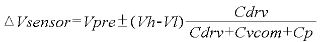
<수식2>
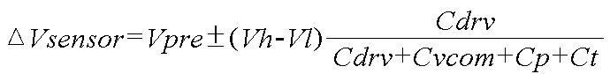
(여기서,  는 터치검출부에서 검출된 전압이며,Vh는 드라이빙 커패시터에 인가되는 하이 레벨 전압이며, Vl은 드라이빙 커패시터에 인가되는 로우 레벨 전압이며, Cdrv는 드라이빙 커패시턴스이며, Cvcom은 공통전극커패시턴스이며, Cp는 기생커패시턴스이며, Ct는 터치커패시턴스임.)
또 다른 실시예에 따르면, 상기 터치검출부(14)는 드라이빙 백(Driving Back)의 크기에 대응하여 상기 터치패드(10)에 대한 터치입력수단의 터치면적을 검출한다.
또 다른 실시예에 따르면, 상기 터치검출부(14)는 검출된 전압을 증폭하는 증폭기(18)를 포함한다.
또 다른 실시예에 따르면, 터치를 검출 중인 터치패드(10)와 연결된 센서신호선(22)의 좌우에 존재하며 터치 비검출중인 센서신호선(22)은 플로팅상태이다.
또 다른 실시예에 따르면, 터치를 검출 중인 터치패드(10)와 연결된 센서신호선(22)을 제외한 터치패드(10)는 플로팅상태이다.
또 다른 실시예에 따르면, 터치를 검출 중인 터치패드(10)와 연결된 센서신호선(22)의 좌우에 존재하며 터치 비검출중인 터치패드(10)는 터치검출부의 충전수단(12)이 턴 온(Turn on) 되기 이전에 플로팅 상태를 갖는다.
또 다른 실시예에 따르면, 터치를 검출 중인 터치패드(10)와 연결된 센서신호선(22)을 제외한 터치패드(10)는 터치검출부의 충전수단(12)이 턴 온(Turn on) 되기 전에 플로팅 상태를 갖는다.
또 다른 실시예에 따르면, 터치검출부(14)에 접속된 드라이빙 커패시터()에 드라이빙 전압이 인가된 후 터치검출부(14)에 접속된 터치패드(10)가 터치검출부(14)에서 분리된다.
또 다른 실시예에 따르면, 터치검출부에 접속된 드라이빙 커패시터에 드라이빙 전압이 인가된 후 1ns 내지 100us 이내에 터치검출부에 접속된 터치패드가 터치검출부(14)에서 분리된다.
또 다른 실시예에 따르면, 상기 터치검출부에서 분리된 터치패드는 터치검출부에서 터치 센싱이 완료된 후 터치검출부에 재 접속되거나 소정의 전압이 인가된다.
또 다른 실시예에 따르면, 상기 소정의 전압은 그라운드(GND) 또는 일정 크기의 DC 전압이다.
또 다른 실시예에 따르면, 터치검출부의 터치센싱 동작이 완료된 후, 플로팅된 터치 비검출 터치패드(10)에는 소정의 전압이 인가된다.
또 다른 실시예에 따르면, 상기 소정의 전압은 그라운드(GND) 또는 일정 크기의 DC 전압이다.
또 다른 실시예에 따르면, 터치패드(10)와 연결된 터치신호선이 TDI(Touch Drive IC)와의 연결부에 접속되는 구간의 저항이 -100% 내지 +100%에 포함되는 복수개의 터치패드가 존재한다.
또 다른 실시예에 따르면, 상기 복수개의 터치패드에 대하여, 상기 터치검출부에 접속된 터치패드의 분리시간은 동일하게 적용된다.
본 발명의 드라이빙 백(Driving Back) 현상을 이용한 터치 검출수단, 검출방법 및 터치스크린패널과, 그러한 터치스크린패널을 내장한 표시장치에 따르면, 표시장치의 공통전극이 소정 주파수로 교번하는 공통전압 레벨을 갖는 경우이거나, 표시장치의 공통전극이 DC 레벨이거나, 그렇지 않으면 표시장치의 공통전극이 규정되지 않은 불특정 주파수로 교번하는 경우에 있어서, 공통전압의 상태변화를 검출하고, 상태변화 시점을 회피하여 터치검출부에 연결된 드라이빙 커패시터를 통해 구동전압을 인가하고, 터치입력에 의해 부가된 터치커패시턴스에 의해 터치검출부에서 드라이빙 백(Driving Back)이 발생하는 것을 검출하여 터치신호를 획득함으로써, 노이즈, 커플링 현상이나 기타 요인에 의해 생성되는 기생커패시턴스 등에 의한 영향이 최소화되고, 신호의 오인식이 발생하지 않으며, 터치입력을 비교적 높은 전압레벨로 검출함으로써 터치입력수단의 단면이 작아도 신호의 포착이 용이하고 스타일러스 펜 입력이 가능하며, 드라이빙 백(Driving Back)의 크기에 따라 터치입력수단의 터치면적 점유율을 구함으로써 터치 해상도를 높이고 미세한 필기 및 드로잉이 가능하며, 액티브영역을 단일 레이어로 구성할 수 있어 제조공정이 간소화되고 수율이 양호한 효과가 있다.
도 1은 종래 터치스크린패널의 일예를 보인 사시도
도 2는 종래 터치스크린패널의 다른 예를 보인 평면구성도
도 3은 도 2의 터치스크린패널이 표시장치 위에 설치된 예를 보인 단면도
도 4는 도 3에서 터치커패시턴스를 검출하는 등가 회로도
도 5는 액정표시장치의 공통전압 파형을 예시한 파형도
도 6은 통상적인 3단자형 스위칭소자를 개념적으로 묘사한 도면
도 7은 터치입력을 검출하는 원리를 예시한 도면
도 8은 본 발명에 따른 터치검출수단의 기본적인 구조를 보인 회로도
도 9a 및 9b는 TDI의 내압과 프리차지 전압의 상관관계를 설명한 도면
도 10은 터치검출부의 구성에 관한 본 발명의 실시예를 도시한 도면
도 11은 터치검출회로부의 구성에 관한 본 발명의 또다른 실시예를 도시한 도면
도 12는 터치패드 구성의 일예를 보인 단면도
도 13은 터치패드 구성의 다른예를 보인 단면도
도 14a 및 도 14b는 면적을 이용한 제스쳐의 실시예를 도시한 도면
도 15a 내지 15c는 면적을 이용한 제스쳐의 또 다른 실시예를 도시한 도면
도 16은 터치신호를 검출하는 과정을 보인 파형도
도 17은 공통전압 검출회로에 관한 본 발명의 실시예
도 18은 공통전압 검출회로에서 검출된 공통전압의 파형도
도 19는 공통전압 검출회로에 관한 본 발명의 상세한 실시예를 도시한 도면
도 20은 공통전압 검출오류 발생 시 복구하는 방법에 관한 실시예를 도시한 도면
도 21은 공통전압 요소 추출을 위한 factory calibration을 위한 흐름도
도 22는 공통전압에 동기하여 터치신호를 검출하는 방법에 관한 본 발명의 실시예를 도시한 도면
도 23은 실제 검출된 공통전압의 예를 도시한 도면
도 24는 레지스터 설정에 따라 Vdrv의 크기가 변하는 실시예를 도시한 도면
도 25는 터치스크린패널의 실시예에 관한 본 발명의 실시예를 도시한 도면
도 26a 내지 도 26c는 터치패드의 다양한 구성에 관한 실시예를 도시한 도면
도 27은 공개특허중 도면5에 표시된 터치스크린패널이 실시예를 도시한 도면
도 28은 터치패드의 상하로 센서신호선을 배선하는 종래의 실시예를 도시한 도면
도 29는 본 발명에 사용되는 차동증폭기의 일 실시예를 도시한 도면
도 30은 증폭기 출력에 ADC 변환부가 접속된 실시예를 도시한 도면
도 31은 factory calibration 방법을 도시한 흐름도
도 32는 RTC를 시행 영역 설정을 위한 본 발명의 실시예를 도시한 도면
도 33은 종래 정전용량방식 터치신호 검출에 관한 일 실시예를 도시한 도면
도 34는 횡전계모드 LCD 기판의 TFT 구성에 관한 도면
도 35는 횡전계모드 LCD 기판의 백그라운드 구성에 관한 종래의 실시예를 도시한 도면
도 36은 횡전계모드 LCD 기판에 적용된 본 발명의 단면도
도 37은 횡전계모드 LCD 기판에 적용된 본 발명의 정면도.
도 38은 터치패드가 백그라운드로 사용되는 본 발명의 실시예를 도시한 도면
도 39는 센서신호선(22)의 레이아웃에 관한 본 발명의 실시예를 도시한 도면
도 40a 내지 40c는 터치검출부와 센서신호선 사이의 공간 충전부에 관한 본 발명의 실시예를 도시한 도면
도 41은 도전체에 의한 터치 검출오류의 일 실시예를 도시한 도면
도 42는 Non Sensing Pad의 open에 관한 본 발명의 실시예를 도시한 도면
도 43은 Sensing Pad의 open에 관한 본 발명의 실시예를 도시한 도면
도 44a 및 44b는 터치센서에서 검출되거나 연산한 data에 의해 터치좌표를 추출하는 본 발명의 실시예를 도시한 도면
도 45는 터치패드로 터치신호와 공통전압을 검출하는 본 발명의 실시예를 도시한 도면
도 46은 기능키 사용에 관한 실시예를 도시한 도면
도 47은 기능키 구현에 관한 본 발명의 실시예를 도시한 도면
도 48은 기능키에 적용되는 레지스터 설정에 관한 일 실시예를 도시한 도면
도 49는 기능키패드의 구조에 관한 본 발명의 실시예를 도시한 도면
도 50은 터치스크린패널의 에지부 구성에 관한 종래의 실시예를 도시한 도면
도 51은 터치스크린패널의 에지부 구성에 관한 본 발명의 실시예를 도시한 도면
도 52는 복수의 TDI가 사용된 본 발명의 실시예를 도시한 도면
도 53은 정전기를 방전시키기 위한 본 발명의 실시예를 도시한 도면
도 54는 터치스크린패널을 내장한 표시장치의 단면도
도 55는 터치스크린패널을 내장한 표시장치의 분해사시도
도 56은 터치그룹 결정에 관한 본 발명의 실시예를 도시한 도면
이하, 본 발명의 바람직한 실시예를 첨부된 도면 및 실시예를 참조하여 상세히 설명한다.
우선, 본 발명은 드라이빙 백(Driving Back) 현상을 이용한 터치 검출수단, 검출방법 및 터치스크린패널과, 그러한 터치스크린패널을 내장한 표시장치에 관한 것으로서, 종래의 터치 검출수단이 손가락 등의 접촉에 의한 커패시턴스의 크기를 검출하는 방식인 것과 달리, 부가된 드라이빙 커패시터(Driving Capacitor)에 교번하는 구동전압을 인가할 때, 터치커패시턴스의 크기 차이에 의해 발생하는 드라이빙 백(Driving Back) 현상을 검출하는 방식이다. 본 발명에 따른 터치 검출 시스템은 터치 미발생시 드라이빙 커패시터 및 공통전극 커패시턴스 및 기생커패시턴스로 인해 발생하는 드라이빙 백 현상에 의한 전압과, 터치 발생에 의해 터치커패시턴스가 부가될 때 드라이빙 백 현상에 의해 발생하는 전압의 크기를 비교하고, 두 전압의 크기 차이를 추출(Extraction)함으로써, 외부의 노이즈나 기생커패시턴스 등에 의한 영향이 최소화 되며, 보다 안정적으로 터치신호를 획득할 수 있다.
본 발명에서 언급되는 표시장치는 LCD, PDP, OLED 중 어느 하나이거나, 기타 화상을 표시하는 모든 수단을 의미한다.
위에 나열한 표시장치 중 LCD는 액정의 구동을 위해 공통전압(Vcom)을 필요로 한다. 일예로서, 휴대기기용 중소형 LCD에서는 소비전류를 감소시키기 위하여 공통전극의 공통전압이 하나 또는 복수의 게이트라인별로 교번하는 Line inversion 방식을 사용한다. 다른 예로서, 대형 LCD는 공통전극의 공통전압이 일정한 DC 레벨을 가지며 도트 인버젼(Dot Inversion) 구동방식을 사용한다. 또 다른 예로서, 횡전계 모드 LCD의 경우, 공통전극은 LCD TFT 기판의 일부영역에 형성되어 라인인버전이나 도트인버전 구동방식에 의해 화상이 표시된다. 이러한 횡전계모드 LCD의 경우, 백 그라운드(Back Ground)가 배면 ITO를 통해 외부로 노출된 칼라필터 전체에 공통으로 형성되며, ESD 차단을 위해 그라운드 신호와 접지시킨다.
본 발명에서는 위와 같이 공통전압(Vcom)이 인가되는 전극 이외에, 표시장치 내에서 공통으로 역할하는 모든 전극들을 공통전극이라 칭하기로 하며 표시장치의 공통전극에 인가되는 교번전압이나 DC 전압 또는 불특정 주파수로 교번하는 형태의 전압을 공통전압이라 칭하기로 한다.
본 발명은 손가락이나 이와 유사한 전기적 특성을 갖는 터치입력수단의 비접촉 터치입력을 검출한다. 여기서 비접촉 터치입력이라 함은 손가락 등의 터치입력수단이 기판에 의해 터치패드과 소정 거리 이격된 상태에서 터치입력을 하는 것을 의미한다. 터치입력수단이 기판의 외면에 대하여는 접촉될 수 있다. 하지만 이 경우에도 터치입력수단과 터치패드은 비접촉 상태를 유지한다. 따라서, 터치패드에 대한 손가락의 터치 행위는 접근이라는 용어로 표현될 수 있다. 한편, 기판의 외면에 대하여는 손가락이 접촉된 상태일 수 있으므로, 기판에 대한 손가락의 터치 행위는 접촉이라는 용어로 표현될 수 있다. 본 명세서에서 접근과 접촉은 위와 같은 의미로 통용된다.
또한, 이하에서 설명되는 ~부와 같은 구성들은, 특정기능을 수행하는 단위 기능 요소(Unit Function Element)들의 집합체로서, 예를 들면 어떤 신호의 증폭기는 단위 기능 요소이며 증폭기나 신호변환기들이 모인 집합체는 신호변환부로 명명할 수 있다. 또한, ~부는 더 큰 구성요소 또는 ~부에 포함되거나, 더 작은 구성요소들 및 ~부들을 포함할 수 있다. 또한, ~부는 자체적으로 독자적인 CPU를 가질 수도 있다.
이하의 도면에서 여러 층 및 영역을 명확하게 표현하기 위하여 두께나 영역을 확대하여 나타내었다. 명세서 전체를 통하여 유사한 부분에 대해서는 동일한 도면부호를 사용하였다. 층, 영역, 기판 등의 부분이 다른 부분 위에 또는 상면 있다고 할 때, 이는 다른 부분 바로 위에 있는 경우 뿐 아니라 그 중간에 또 다른 부분이 있는 경우도 포함한다. 반대로 어떤 부분이 다른 부분 바로 위에 있다고 할 때에는 중간에 다른 부분이 없는 것을 뜻한다.
또한, 본 명세서에 기재된 신호는 특별한 언급이 없는 한, 전압 또는 전류를 총칭한다.
또한, 본 명세서에서 커패시턴스는 물리적인 크기를 나타내며, 정전용량과 동일한 의미로 사용된다. 한편,커패시터는 물리적인 크기인 커패시턴스를 갖는 소자(Element)를 지칭한다. 커패시턴스는 설계된 값 및 공정에 의해 만들어 지기도 하며, 임의의 거리로 평행한 두개의 신호선 사이에 자연적으로 생성되는 것처럼 간접적으로 만들어 지기도 한다. 본 명세서에서는 직접 만들어진 커패시터나 간접적으로 형성된 커패시터 모두를 구분하지 않고 커패시터로 명명한다.
또한, 본 명세서에서신호(signal)를 인가(forcing)"한다는 의미는 이미 어떤 상태를 유지하고 있던 신호의 레벨(Level)이 바뀌거나, 플로팅(Floating) 상태에서 어떤 신호에 접속된다는 의미이다. 예를 들어, 스위칭소자의 온/오프 제어단자에 신호를 인가한다는 의미는, 기존의 로우(Low) 레벨 전압이 하이(Hi)레벨로 바뀐다는 의미로 사용되기도 하며, 아무런 신호도 없이 플로팅된 상태의 스위칭소자의 온/오프 제어단자에 스위칭소자를 턴 온 / 턴 오프를 하기 위한 어떤 전압을 인가한다는 의미로도 사용될 수 있다.
또한, 본 발명에서 드라이빙 백 (Driving back) 현상 또는 드라이빙 백 (Driving back)은 동일한 의미로 사용되며 "D/B"로 축약하여 사용한다.
또한 본 발명에서 터치드라이브IC(Touch Drive IC)는 TDI로 축약하여 사용한다.
또한 본 발명에서, 터치가 발생하지 않은 경우에 D/B에 의한 전압을 검출하고 또한 터치가 발생했을 때 D/B에 의한 전압을 검출하여 두 전압의 상관관계(Relationship)을 이용하여 터치여부 및 터치수단의 접촉면적을 판단하므로, D/B 현상에 의한 전압을 검출한다는 의미와 터치신호를 검출한다는 의미는 동일하게 사용된다.
도 6은 본 발명에서 충전수단의 한 예시로서 사용되는 스위칭 소자 중 3단자형 스위칭소자를 개념적으로 묘사한 것이다. 도 6을 참조하면, 3단자형 스위칭소자는 통상 온/오프 제어단자(Cont), 입력단자(In), 출력단자(Out)의 3개 단자를 구비한다. 온/오프 제어단자는 스위칭소자의 온/오프를 제어하는 단자로서, 이 단자에 소정 크기의 전압이나 전류를 인가하면 입력단자로 인가된 전압 또는 전류는 출력단자에 전압이나 전류형태로 출력된다.
본 발명에서 충전수단으로 언급되는 3단자형 스위칭소자는 예를 들어, 릴레이(Relay), CMOS(Complementary Metal Oxide Semiconductor) 스위치 또는 PMOS 또는 NMOS, BJT(Bipolar Junction Transistor), FET(Field Effect Transistor), MOSFET(Metal Oxide Semiconductor Field Effect Transistor), IGBT(Insulated Gate Bipolar Transistor), TFT(Thin Film Transistor), OPAMP이며, 이들끼리의 동종간 또는 이종간의 결합에 의해 형성될 수도 있다.
릴레이는 3단자형 소자 외에 4단자형 소자도 사용될 수 있다. 본 발명에 사용될 수 있는 충전수단으로는, 입출력 단자의 개수에 상관없이 입출력을 온/오프할 수 있는 제어단자를 갖고 있으며 온/오프 제어단자에 의해 입출력이 온/오프되는 모든 소자가 사용될 수 있다.
한편, 3단자형 스위칭소자의 일예로서 CMOS 스위치는 PMOS와 NMOS의 상호 조합에 의해 형성되며, 입출력 단자는 상호 연결되어 있으나, 온/오프 제어단자는 개별적으로 존재하여 동일한 제어신호에 같이 연결되거나 개별적인 제어신호에 별도로 연결되어 온/오프 상태가 결정된다. 릴레이(Relay)는 제어단자에 전류를 인가하면 입력단자에 인가된 전압이나 전류가 손실 없이 출력되는 소자이며, BJT는 베이스(Base)의 문턱값(Threshold Value)(Threshold voltage)보다 높은 전압을 베이스에 인가한 상태에서 베이스단자에 전류를 흘리면, 일정량 증폭된 전류가 콜렉터(Collector)에서 에미터(Emitter)로 흐르는 소자이다. 또한 TFT는 LCD나 AMOLED등의 표시장치를 구성하는 화소부에 사용되는 스위칭소자로서 제어단자인 게이트(Gate)단자, 입력단자인 소스(Source)단자 및 출력단자인 드레인(Drain)단자로 구성되며, 게이트단자로 드레인단자에 인가된 전압보다 문턱값(Threshold Value) 이상되는 전압을 가하면, 도통되면서 게이트단자에 인가된 전압의 크기에 종속되는 전류가 입력단자에서 출력단자로 흐르는 소자이다.
본 발명의 구체적인 실시예에 대하여 설명하기에 앞서, 도 7을 참조하여 본 발명에서 터치입력을 검출하는 원리에 대하여 간략하게 설명한다. 도 7의 예시에서, 터치패드(10)에 손가락(25) 또는 이와 유사한 도전성의 터치수단이 접근했을 때 터치패드(10)와 손가락(25)이 "d"의 간격으로 이격되며, "A"라는 대향면적을 갖는다고 가정하자. 그러면, 도 7의 우측 등가회로 및 수식에서 보이듯이, 손가락(25)과 터치패드(10) 사이에는 커패시턴스 "C"가 형성된다. 커패시턴스 "C"를 가지는 터치패드(10)의 신호입력선에 전압이나 전류의 신호를 공급하고 커패시턴스 C"의 크기를 가지는 커패시터에 전하량 "Q"의 크기를 갖는 전하가 축적될 때 커패시터는 V=Q/C라는 관계식으로 전하를 축적할 수 있다. 본 발명에서는 터치검출부와 접속된 센세패턴(10)에 커패시턴스 "C"의 크기와 상관관계를 가지는 드라이빙 백(Driving Back)이 발생할 때 이것을 이용하여 터치를 검출한다.
도 8은 본 발명에 따른 터치검출수단의 기본적인 구조를 보인 회로도이다. 이를 참조하면, 본 발명에 따라 특화된 터치검출수단은, 충전수단(12), 터치패드(10), 센서신호선(22), 드라이빙 커패시터(Cdrv), 공통전극커패시터(Cvcom) 및 터치검출부(14)로 구성된 기본적인 구조를 갖는다.
충전수단(12)은 터치패드(10)에 프리차지(Precharge) 신호를 공급하고, Cont"로 명명된 "온/오프 제어단자"에 인가된 턴 오프(Turn Off) 신호에 턴 오프되어 출력단(12-1)을 하이 임피던스로 만든다.
프리차지(Precharge) 신호는 터치신호 검출 이전에 충전수단(12)의 출력단(12-1)에 연결된 모든 커패시터에 DC 전압을 인가하여 이들 커패시터들을 충전하는 전압이다. 따라서 충전수단(12)은 온/오프 제어단자에 공급되는 제어신호에 따라 스위칭동작을 수행하는 스위칭소자이거나, 제어신호에 따라 신호를 공급하는 OPAMP 등의 선형소자이다.
도 8의 실시예와 같이 충전수단(12)으로 3단자형 스위칭소자가 사용될 경우, 온/오프 제어단자에 공급되는 제어신호와 입력단자에 공급되는 신호를 이용하여, 필요한 시점에 적절한 충전전압을 터치패드(10), 드라이빙 커패시터(Cdrv), 공통전극 커패시터(Cvcom)등 충전수단(12)의 출력부(12-1)에 접속된 모든 커패시터에 공급할 수 있다. 충전 전압은 영 볼트(Zero Volt)를 포함한 DC 전압 및 구형파나 삼각파, 또는 싸인파(Sine Wave)와 같이 교번하는 AC 전압이 사용될 수 있다.
이러한 충전전압은, 본 발명의 터치검출 시스템이 집적된 터치 드라이브 IC(Touch Drive IC, 이하 TDI)에서 사용되는 전압과 연관성을 갖는다. 이러한 연관성을 도 9a 및 도 9b를 예로 들어 설명하면 다음과 같다.
TDI의 내압이 5V로서, 5V이상의 전압이 TDI에 공급될 시 TDI가 파손된다고 가정하면, TDI 내부에서 동작하는 회로의 동작전압은 5V를 초과하면 안 된다. 도 9a 내지 도 9b의 실시예와 같이 후술하게 될 D/B에 의한 전위차가 3V라고 가정하자. 이때 도 9a과 같이 D/B이 발생하기 이전에 충전수단(12)의 출력부(12-1)의 전압이 3V라고 하면 D/B에 의한 충전수단의 출력부(12-1)의 전압은 6V이며 이는 TDI의 내압인 5V를 초과하므로 TDI(30)는 파손영역에 놓이게 된다.
이러한 문제점을 해결하기 위해 도 9b와 같이 충전수단이 턴 온 된 상태에서 충전수단의 입력부에 1V를 인가하여 충전수단의 출력부에 접속된 모든 커패시터에 1V를 충전하게 되면, 전술한 드라이빙 백에 의한 3V의 전위차가 발생하더라도 출력부(12-1)의 전위는 4V이므로 TDI(30)는 안전영역에서 동작하게 된다.
이와 같이, 본 발명의 일 실시예는 TDI의 내압에 기초하여 드라이빙 백 발생시의 최대 전압의 크기를 조절하는 충전 전압을 제어하는 기능을 구비할 수 있다.
도 10은 본 발명에 따른 터치검출부(14)의 구성에 관한 실시예이다. 도 10을 참조하면, 충전수단(12)의 출력부(12-1) 및 출력부(12-1)와 접속된 모든 커패시터들은 터치검출부(10)와 접속된다. 후술하게 될 D/B 현상은 충전수단(12)의 출력부(12-1)와 연결된 커패시터에서 발생하므로, D/B에 의해 발생한 전압은 터치검출부(14)의 Buffer(14-1)로 전달된다. Buffer(14-1) 입력단은 통상 하이 임피던스(High Impedance, 이하 Hi-z라 칭함)이므로, 충전수단의 출력부(12-1)가 Hi-z 상태가 되면 충전수단의 출력부(12-1)와 Buffer(14-1) 사이에 접속된 모든 커패시터들도 Hi-z 상태가 된다. 본 실시예에서는 충전수단의 출력부(12-1)가 Buffer(14-1)에 직접 접속되는 것을 예시하였으나, Buffer(14-1) 대신에 MOS의 gate나 TFT의 gate등 입력이 Hi-z 상태인 모든 소자의 단자에 접속될 수 있다. 충전수단의 출력부(12-1)와 터치검출부(14)를 Hi-z 상태로 만드는 이유는, 후술하게 될 D/B 현상이 Hi-z인 상태에서 검출해야 검출시간을 길게 할 수 있기 때문이다. 즉, Hi-z 상태에서는 고립된 전하의 방전경로가 없으므로 D/B에 의해 형성된 전압의 레벨이 최소한의 변형으로 오래 유지된다.
Buffer(14-1)에서 출력된 신호는 증폭기(14-2)로 입력된다. 증폭기(4-2)의 입력단이 Hi-z인 경우라면, 도 10의 P점(Point)은 증폭기(14-2)의 입력단에 바로 접속되어도 무방하다.
P점 신호의 크기(Level)가 낮아 증폭되어야 하는 경우, 다양한 증폭기를 사용하여 신호를 증폭할 수 있으나, 차동증폭기(Differential Amplifier)를 사용하는 것이 바람직하다. 왜냐하면, P점은 후술하게 될 프리차지전압(또는 충전전압)으로 충전되는데, 증폭과정에서 이러한 충전전압은 차동증폭기를 통해 제거되고, P점에서 D/B 현상에 의해 발생한 전압만을 증폭하는 것이 가능하기 때문이다.
차동증폭기를 사용할 때 충전전압 같은 DC offset을 제거하기 위해서는, 차동증폭기의 negative 단자에 DC 전압이 인가되어야 한다. 이러한 DC 전압을 인가하기 위하여 DAC(14-4)가 사용되거나 Ref 전압(14-5)이 사용되어야 하는데, Ref 전압은 기준전압(Voltage Reference)로서 일정 전위를 가진 DC 전압이며, 도 25에서 후술하게 될 전원부(47)에서 생성된다.
도 10에서는 하나의 터치패드(10)에 대응하여 하나의 ADC 만을 사용하는 것으로 도시하였으나, 도 10과 같은 터치 검출 회로가 복수개 사용되면 ADC도 복수개 사용할 수 있으며 ADC를 많이 사용할 수록 신호의 연산시간을 줄일 수 있는 장점이 있다.
도 10에 도시하지는 않았으나, 터치검출부(14)안에 표시된 여러 기능부 사이에는 필터(filter)가 사용될 수 있다. 예를 들어, Buffer(14-1)의 전단(Previous stage)에도 필터가 사용될 수 있으며, 증폭기(14-2)의 전단이나 증폭단(14-2)에서도 필터가 사용될 수 있다. 이러한 필터는 대역폭 로우패스 필터(Bandwidth Low Pass Filter)나 하이패스 필터(Bandwidth High Pass Filter) 또는 GCF(Grass Cut Filter), Ranking Filter, 쵸핑(Chopping)에 의한 평균필터(Average Filter)등 다양한 필터들이 사용될 수 있다.
터치패드(10)는 투명도전체나 메탈(Metal)로 형성된다. 터치패드(10)가 표시장치 위에 설치되어 투명도전체로 형성되는 경우, 투명도전체는 ITO(Indium Tin Oxide), ATO(Antimony Tin Oxide), CNT(Carbon Nano Tube), IZO(Indium Zinc Oxide) 등의 도전성 투명 물질 또는 이와 유사한 도전특성을 갖는 투명 물질로 형성된다. 만약, 터치패드(10)가 표시장치와 같이 사용되지 않는 터치 키보드, 냉장고나 모니터 등의 터치키로 응용될 경우 터치패드(10)는 메탈(metal) 등의 비투과 물질로 형성될 수도 있다.
터치패드(10)는 다양한 형태로 형상화(Patterning) 될 수 있다. 예컨대, 터치스크린패널(50)의 액티브영역에서 고립된 섬(island)들이 매트릭스 형태로 배열되는 도트 매트릭스 형태이거나, 선형의 패턴들이 터치스크린패널(50)을 종횡하도록 배열될 수 있다. 터치패드(10)의 형태에 대하여는 후술되는 실시예에서 상세하게 설명하기로 한다.
센서신호선(22)은 터치패드(10)에 손가락(25) 또는 이와 유사한 도전특성을 갖는 터치수단(예컨대, 터치펜 등과 같은)이 접근할 때 형성된 커패시터의 일극(Polarity)을 터치검출부(14)에 접속하는 신호선(Signal Line)으로서, 터치패드(10)와 마찬가지의 도전성 투명 물질로 형성될 수 있으며, 경우에 따라서는 메탈 등의 비투과 물질로 형성될 수도 있다. 센서신호선(22)의 구체적인 실시예도 후술되는 실시예에서 설명하기로 한다.
드라이빙 커패시터(Cdrv)는 본 발명에서 터치 검출을 위한 드라이빙전압을 인가하기 위한 구성으로서, 일단은 터치검출부(14)에 연결되며 타단으로는 드라이빙전압이 인가되며 드라이빙전압에 의한 D/B 현상이 발생하게 된다.
도 8에 도시한 바와 같이, 충전수단(12)의 출력부(12-1)는 터치검출부(14)에 접속된다. 그리고, 드라이빙 커패시터(Cdrv)의 일측은 충전수단(12)의 출력부(12-1)에 접속되며 드라이빙 커패시터(Cdrv)의 타단에는 검출신호가 인가된다. 검출신호는 서로 다른 복수개의 전위를 교번하는 전압으로서, 구형파, 사인파, 삼각파 등의 주기성 또는 비주기성 파형이며, 교번하는 드라이빙전압의 크기에 비례하는 D/B 전압이 터치검출부(14) 또는 터치패드(10)에서 유도되어 검출된다. 검출되는 D/B 전압은 터치검출부(14) 및 터치패드(10) 및 충전수단(12)의 출력부(12-1)의 교점에서 검출되므로, 본 명세서를 통틀어 터치패드(10)나 터치검출부(14) 또는 충전수단(12)의 출력부(12-1)에서 D/B 신호가 검출된다는 의미는 동일한 위치에서 D/B 신호가 검출된다는 의미이다.
도 8의 공통전극 커패시터(Cvcom)는 터치패드(10)가 표시장치의 공통전극과 대향할 때 형성되는 커패시턴스이며, 일측은 터치검출부(14)에 접속되고 타측에는 공통전압이 인가된다. 이때, 공통전압과 직접 접속되어 인가될 수도 있지만, 통상은 유리나 공기등의 매질을 통해 전자기적으로 유도되어 인가된다. 예를 들면, 도 12의 터치패드(10)는 손가락(25)과 같은 터치수단과 터치 정전용량(Ct)을 형성하며 또한 컬러필터(215)를 사이에 두고 공통전극 커패시터(Cvcom)을 형성한다.
도 11은 스위칭소자의 일 실시예로 MOS나 TFT 또는 FET가 사용되고, 터치검출부(14)에 ADC(Analog to Digial Converter)가 사용된 경우이다. ADC는 검출된 아날로그 신호를 디지털로 변환하는 기능을 하며, 본 실시예에서 검출된 터치신호를 디지털로 변환하여 도 25의 신호처리부(35)나 CPU(40)에 전달하는 기능을 수행한다.
도 11에 보이는 바와 같이, 인체의 손가락(25)이 터치패드(10)에 일정 간격으로 접근하면, 손가락(25)과 터치패드(10) 사이에는 "Ct"라고 하는 터치커패시턴스(Ct)가 형성된다. Ct는 도 7의 관계식에 의해 설정되는 값으로서, 터치수단과 터치패드(10)의 간격, 대향면적 등을 조절하는 것에 의해 자유롭게 조정될 수 있다. 예컨대, 터치패드(10)의 면적을 크게 구성하면 도 7의 관계식에 따라 Ct 역시 크게 형성된다. 반대로, 터치패드(10)의 면적을 작게 구성하는 것으로서 Ct는 작게 형성된다. 일실시예로, Ct는 수 fF(femto F) 내지 수십 uF(micro F)으로 설계될 수 있다.
도 11의 Cp는 기생커패시터로서, Ct처럼 수식에 의해 형성되거나 Cdrv와 같이 제조가능한 커패시터 이외의 커패시터 값들의 총 합이며, 터치검출부(14)에 일측이 접속되고 임의의 그라운드에 타측이 접속된 커패시터로 모델링 할 수 있다. 따라서 그라운드가 서로 다른 복수개의 기생커패시터(Cp)가 형성될 수 있으나, 본 명세서에서는 하나의 그라운드만을 가정하여 이에 연결된 하나의 기생커패시터만을 표시하였다. 이러한 기생커패시터(Cp)는 센서신호선(22)과 표시장치 사이에 발생하는 기생커패시터, 또는 터치패드(10)가 도 25와 같이 도트 매트릭스 형태로 복수개 설치되어, 이들과 연결된 센서신호선(22)이 상호 평행하게 배선될 때 센서신호선(22) 사이에 발생하는 기생커패시터, TDI가 터치패드(10)와 연결될 때 연결부에서 발생하는 기생커패시터, 또는 TDI 내부에서 센서신호선과 연결된 회로부가 주변 회로들과의 간섭에 의해 발생하는 기생커패시터 등 다양한 형태의 기생커패시터가 있다. 후술하게 될 <수식1>이나 <수식2>에 따르면, 이러한 기생커패시터들은 수식의 분모에 삽입되어 D/B 신호를 낮추는 역할을 하므로, 가급적 기생커패시터는 없을 수록 터치 검출에 유리하다.
다시 도11을 참조하면, 충전수단(12)의 입력단자에는 프리차지전압(Pre charge Voltage)인 Vpre가 인가되고, 온/오프 제어단자(cont)에 인가되는 제어전압(Vg)에 의해 스위칭소자가 턴 온(Turn on)될 때 프리차지전압(Vpre)은 출력부(12-1)를 통해 출력된다. 따라서 충전수단(12)의 출력부(12-1)에 접속된 모든 커패시터들은 프리차지전압(Vpre)으로 충전된다.
일실시예로 Vpre가 3V이며 Vg가 0V(Zero Volt)에서 10V로 변화될 때 스위칭소자가 턴 온이 된다고 한다면, 스위칭소자의 턴 온 이후 드라이빙 커패시터(Cdrv), 터치커패시터(Ct), 기생커패시터(Cp)가 접속된 터치검출부(14)의 전위는 3V이다. P점을 충전한 이후 스위칭소자의 제어전압(Vg)을 10V에서 0V로 하강시켜 스위칭소자를 턴 오프 시키면 터치검출부인 P점은 Hi-z가 되어 P점의 전하는 고립되며, 드라이빙 커패시터(Cdrv)에 교번하는 드라이빙전압을 인가하면, P점에서 검출되는 전압의 크기는 드라이빙전압의 크기에 비례하고 P점에 접속된 커패시터들의 크기와 상관관계를 가지는 드라이빙 백(Driving back) 현상이 발생한다.
이때, Cdrv, Cp 및 Cvcom을 고정된 값이라고 가정하고, 드라이빙 커패시터(Cdrv)에 인가되는 드라이빙전압의 크기도 일정하다고 가정하면, P점에서 D/B 현상에 의해 검출되는 전압의 크기는 터치커패시터(Ct)에 종속된다. 따라서, 터치검출부(14)에서 검출되는 전압은 터치커패시터(Ct)의 크기에 따라 변화되므로 이러한 드라이빙 백(Driving Back) 현상에 의한 드라이빙전압의 차이를 검출하면, 터치의 유무 및 터치패드(10)와 터치수단(25)의 대향면적(또는 터치면적)을 연산하는 것이 가능하며, 터치지점을 찾는 것도 가능하게 된다.
도 12는 본 발명에 따른 터치패드 구성의 일예를 보인 단면도이고, 도 13은 본 발명에 따른 터치패드 구성의 다른 예를 보인 단면도이다. 도 12는 터치패드(10)가 표시장치와 별체로 형성된 기판에 실장 되는 경우를 예시하며, 도 13은 터치패드(10)가 표시장치 내에 내장된 경우를 예시한다. 도 12 및 도 13을 참조하여 공통전극커패시터(Cvcom)의 형성관계를 설명하면 다음과 같다.
도 12에 도시된 바와 같이 표시장치(200)는 공통전극(220)을 갖는다. AMOLED나 PDP의 경우에는 화질을 표시하기 위해 기능이 부여된 공통전극을 갖지는 않으나, AMOLED의 TFT기판이나 PDP의 구동기판에 형성된 다양한 전위 및 이와 대향하는 터치패드(10) 사이에 도 11의 Cvcom이 형성되므로, AMOLED의 TFT기판이나 PDP의 구동기판에 형성된 다양한 전위로 이루어진 가상의 전위도 공통전극으로 명명하기로 한다.
표시장치(200)는 앞서 언급한 다양한 형태의 표시장치일 수 있으며, 공통전극(220)은 LCD의 Vcom 전극이거나, 기타 다른 유형의 전극일 수 있다. 도 12의 실시예는 표시장치들 중 LCD를 예시하였다.
도 12에 도시된 표시장치(200)는 하측의 TFT기판(205)과 상측의 칼라필터(215) 사이에 액정이 봉입되어 액정층(210)을 형성하는 구조를 갖는다. 액정의 봉입을 위하여 TFT기판(205)과 칼라필터(215)는 그 외곽부에서 실런트(230)에 의해 접합된다. 도시하지 않았지만, 액정패널의 상하로는 편광판이 부착되며, 그밖에도 BLU(Back Light Unit)와, BEF(Brightness Enhancement Film)를 구성하는 광학시트들이 BLU와 같이 설치될 수 있다.
표시장치(200)의 상부에는 도시한 바와 같이 터치스크린패널(50)이 설치된다. 도 12의 예시에서 터치스크린패널(50)은 그 외곽부에서 DAT(Double Adhesive Tape) 등과 같은 접착부재(57)를 매개로 표시장치(200)의 상부에 부착된다. 그리고 터치스크린패널(50)과 표시장치(200) 사이에는 에어갭(58)이 형성되거나 또는 접촉부재(58)로 충전된다. 접촉부재(58)는 투과성 실리콘이나 OCA(Optically Clear Adhesive)나 접착성 레진(Resin)등 터치스크린패널(50)과 표시장치(200)을 부착시키는 소재이다.
표시장치(200)의 공통전극(220)에는 화상표시를 위한 공통전압 레벨이 인가되며 공통전압은 DC이거나 일정 진폭을 소정의 주파수로 교번하는 전압니다. 예컨대, 라인반전을 하는 소형 LCD는 공통전극(220)의 공통전압이 도 5에서와 같이 교번하며, 도트반전을 하는 노트북이나 모니터/TV등의 LCD는 일정크기의 전압인 DC 레벨의 공통전압이 인가된다.
도시한 바와 같이, 터치패드(10)와 표시장치(200)의 공통전극(220) 사이에는 공통전극커패시터(Cvcom)가 형성된다. 만약 터치패드(10)에 어떤 프리차지신호를 인가하면, 공통전극커패시턴스(Cvcom)에는 프리차지 전압에 의해, 공통전압을 그라운드로 하는 프리차지 전압이 충전된다. 예컨대, 프리차지 시점에 공통전압이 5V이며 프리차지 전압이 3V이면 공통전극커패시터에는 5V를 기준으로 3V의 프리차지 전압이 충전된다. 이처럼 공통전극커패시턴스(Cvcom)의 일단은 공통전극(220)의 전위와 전기적으로 접지되어 있으므로, 공통전극(220)이 교번 전압인 경우 공통전극(220)에 인가되는 교번 전압에 의해 공통전극커패시턴스(Cvcom)의 타단인 터치패드(10)에서의 전위는 교번하며 이러한 교번 전위는 D/B 현상을 이용한 터치신호와 중복되면 터치신호 검출에 장애를 일으킬 수 있으므로, D/B 현상을 이용한 터치신호 검출 시에는 이러한 교번하는 공통전압의 rising edge 및 falling edge를 회피하여 검출하여야 한다.
한편, 도면 중 미설명 부호 24는 터치패드(10)을 보호하기 위한 보호층(24)이며 유리나 플라스틱 또는 비닐이나 천(cloth)등이 사용된다.
도 13은 터치패드 구성의 다른 예로서, 표시장치에 터치패드(10)가 내장된 경우의 실시예이다. 도 13을 참조하면, 터치스크린패널(50)은 표시장치의 일부인 칼라필터(215)의 상면에 형성될 수 있다. 도시한 바와 같이 칼라필터(215)의 하부에는 공통전극(220)이 형성되어 있으며 칼라필터의 상면에는 터치패드(10)가 패터닝(Patterning) 되어 있다. 도 13의 실시예에서 보호층(24)은 편광판(Polarizer)으로 대체된다.
도 13의 실시예에서도 공통전극(220)과 터치패드(10) 사이에는 공통전극커패시턴스(Cvcom)가 형성되며, 공통전극에 교번 전압이 인가되면 센서페턴(10)의 전위는 교번전압에 유도되어 교번하게 되고, 이러한 교번 전위에 의해 유도된 D/B 현상에 의한 전압은 드라이빙 커패시터(Cdrv)에 인가되는 교번 드라이빙전압에 의해 유도된 D/B 현상을 이용한 터치신호검출과 중복되면 터치신호에 영향을 미치므로, D/B 현상을 이용한 터치신호 검출시에는 이처럼 교번하는 공통전압의 rising edge 및 falling edge를 회피하여 검출하여야 한다.
다시 도 11을 참조하면, 충전수단(12)의 출력부(12-1)에는 터치패드(10)와 손가락(25)과 같은 도전체 사이에 형성된 터치커패시턴스(Ct) 및 Cdrv, Cvcom, 및 Cp가 연결된다. 따라서 충전수단(12)을 턴 온 시킨 상태에서 입력부(12-2)에 임의의 전압이나 전류 등의 프리차지 신호를 인가하면 Cdrv, Ct, Cvcom, 및 Cp가 프라차지 레벨로 충전되어 터치검출부(14) 입력단의 전위는 프리차지 레벨이 된다. 이후, 만약 충전수단(12)을 턴 오프 시키면 4개의 커패시터에 충전된 신호는 별도로 방전시키지 않는 한 프리차지(또는 충전) 신호 레벨을 유지하게 된다.
충전된 신호를 안정적으로 고립시키기 위해서, 충전수단(12)의 출력부(12-1)와 터치검출부(14)의 입력단은 Hi-z 상태이며, 바람직하게는 적어도 100Kohm 이상의 임피던스를 갖는다. 만약 4개의 커패시터에 충전된 신호를 방전시키면서 터치입력을 관찰하거나, 다른 수단으로 충전된 신호를 고립시키거나, 방전 개시 시점에서 신속하게 신호를 관찰한다면, 터치검출부(14)의 입력단이 반드시 Hi-z이어야 하는 것은 아니다.
터치검출부(14)는 터치패드(10)에서의 신호 레벨이 변동되는지 여부를 검출한다. 바람직하게는, 터치검출부(14)는 터치 미발생시(즉, Ct가 형성되지 않을 때의) D/B 현상에 의해 검출된 전압의 크기에 대비하여, 터치 발생시(즉, Ct가 형성될 때의) D/B 현상에 의해 검출된 전압의 크기 차이를 검출하여 터치신호를 획득한다. 터치검출부(14)는 다양한 소자 또는 회로구성을 가질 수 있다. 후술되는 실시예에서는 터치검출부(14)로서 스위칭소자 및 증폭기가 사용되는 예를 설명하겠으나, 터치검출부(14)의 구성은 그러한 실시예에 국한되지 않는다.
터치 미발생시 드라이빙 커패시터(Cdrv) 및 Cdrv의 일측에 인가되는 드라이빙전압에 의한 버퍼(14-1) 출력은 다음의 <수식1>에 의해 결정된다.
<수식1>

터치 발생시 터치검출부(14)에는 터치커패시턴스(Ct)가 병렬로 부가되므로, 터치검출부(14) 입력단에서 드라이빙 백(Driving Back)에 의해 검출된 전압은 다음의 <수식2>에 의해 결정된다.
<수식2>

위 <수식1> 및 <수식2>에서,  는 터치검출부(14)의 입력단에서 D/B에 의해 발생한 전압이며, Vpre는 프리차지 전압이며, Vh는 드라이빙 커패시터(Cdrv)에 인가되는 드라이빙전압의 하이 레벨 전압이며, Vl은 드라이빙 커패시터(Cdrv)에 인가되는 드라이빙전압의 로우 레벨 전압이며, Vcom은 공통전극커패시턴스이며, Cp는 기생커패시턴스이며, Ct는 터치커패시턴스이다.
터치검출부(14)는 위와 같은 <수식1> 또는 <수식2>에 의해 발생하는 전압을 검출하며, 이에 대하여 상세히 설명하면 다음과 같다.
먼저 <수식1>과 <수식2>를 인용하여 D/B 현상을 다시 정의하면 다음과 같다. D/B 현상이란, 드라이빙 커패시터와 접속된 적어도 하나 이상의 커패시터가 있으며 드라이빙 커패시터의 타측(도 11의 Vdrv 인가부)에 소정 크기의 전압을 교번하며 인가할 때, 커패시터가 공통으로 접속된 지점의 전위는 드라이빙 커패시터의 일측에 인가된 전압의 크기에 비례하며, 공통으로 접속된 커패시터들과 상관관계를 갖는다. 여기서 언급된 상관관계는, 공통으로 접속된 모든 커패시터의 커패시턴스 합(sum)이 분모에 위치하며 드라이빙 커패시턴스가 분자에 위치한다는 의미이다.
<수식1>과 <수식2>의 차이를 보면, <수식2>는 분모에 Ct가 존재한다. 터치커패시턴스 Ct는 터치패드(10)와 손가락같은 터치수단 사이에 형성되는 커패시터이므로, Ct의 크기인 커패시턴스는 터치의 유무에 따라서 또는, 터치수단과 터치패드(10)의 대향거리나 대향면적에 따라서 달라지게 되며, 이러한 Ct의 차이는 <수식1>과 <수식2>로 유도된 전압의 차이를 유발하므로, 이러한 전압차를 검출하면 터치여부나 터치면적 연산이 가능하다.
위 수식들에서 Vh 및 Vl은 드라이빙 커패시터(Cdrv)에 인가되는 드라이빙전압의 하이 레벨 및 로우 레벨이며, D/B 현상은 드라이빙전압이 하이에서 로우로 변화되거나 로우에서 하이로 변화되는 두가지의 경우 모두 발생한다. 만일 Vh=5V인 시점에서 Vl=2V인 지점까지 드라이빙전압이 변화하면 D/B은 -(Vh-Vl)인 -3V에 비례 할 것이며, Vl=2V에서 Vh=5V까지 변화하게 되면 D/B은 (Vh-Vl)인 3V에 비례하게 된다.
드라이빙전압이 로우에서 하이로 교번하는 순간, 드라이빙 커패시터에는 전하가 공급되며 드라이빙 커패시터에 공급된 전하는 드라이빙 커패시터와 병렬로 접속된 모든 커패시터에 공급되어 전위가 상승하므로 D/B에 의한 드라이빙전압은 다음과 같다.
<수식1-1>

또한 드라이빙전압이 하이에서 로우로 교번하는 순간, 드라이빙 커패시터 및 드라이빙 커패시터와 병렬접속된 커패시터들로 부터 전하를 방전시키므로 커패시터들의 전위는 하강하며 D/B에 의한 드라이빙전압은 다음과 같다.
<수식1-2>

이러한 방법은 <수식2>에도 동일하게 적용된다.
한편, Vh와 Vl은 쉽게 설정될 수 있는 값이며 전술한 TDI의 내압을 초과하지 않는 범위내에서 결정될 것이다. 예를 들어, Vpre=3V이며 커패시터들의 상관관계에 의한 값이 0.1이라고 가정하면, Vh=10V에서 Vl=0V로 변화 할때 D/B에 의한 드라이빙전압은, 2V가 될 것이다.
또한, Cvcom은 다음의 <수식3>으로부터 얻을 수 있다.
<수식3>

<수식3>에서은 터치패드(10)와 공통전극(220) 사이에 존재하는 매질들의 복합유전율이다. 도 12의 경우 터치패드(10)와 공통전극(220) 사이에는 유리, 공기층, 편광판 또한 편광판을 유리에 부착하기 위한 접착제가 존재하므로 이들의 복합유전율이 수식3의 이 된다. S1은 터치패드(10)와 공통전극(220)의 대향면적이므로 쉽게 구할 수 있다. 도 12의 예에서와 같이 공통전극(220)이 칼라필터(215)의 하면 전체에 걸쳐 형성된 경우, 대향면적 S1은 터치패드(10)의 면적에 의해 결정된다. 또한, D1은 터치패드(10)와 공통전극(220)간 거리이므로, 매질의 두께에 해당된다.
살펴 본 바와 같이 Cvcom은 쉽게 구할 수 있는 값인 동시에, 설정할 수 있는 값이다.
Ct는 다음의 <수식4>로부터 얻을 수 있다.
<수식4>

<수식4>에서 는 터치패드(10)와 손가락(25) 사이의 매질로부터 얻을 수 있으며 복수의 매질이 사용되면 이들의 복합유전율로 구할 수 있다. 만약, 도 12에서 터치스크린패널(50)의 상면에 강화 글래스를 부착한다면, 강화 글래스의 비유전율에 진공의 유전율을 곱한 값으로부터 유전율 를 얻을 수 있다. S2는 터치패드(10)와 손가락(25)의 대향면적에 해당한다. 만약 손가락(25)이 어떤 터치패드(10)를 모두 덮고 있다면 S2는 터치패드(10)의 면적에 해당한다. 만약 손가락(25)이 터치패드(10)의 일부를 덮고 있다면 S2는 터치패드(10)의 면적에서 손가락(25)과 대향하지 않은 면적만큼 줄어들 것이다. 또한, D2는 터치패드(10)와 손가락(25)간 거리이므로, 터치스크린패널(50) 상면에 올려진 보호층(24)의 두께에 해당할 것이다.
살펴 본 바와 같이 Ct 역시 쉽게 구할 수 있는 값인 동시에, 터치스크린패널(50) 상부에 올려지는 보호층(24) 또는 강화글래스 등의 재질 밑 두께를 이용하여 쉽게 설정할 수 있는 값이다.
<수식4>에 의하면 Ct는 손가락(25)과 터치패드(10)의 대향면적에 비례하므로, 이로부터 터치패드(10)에 대한 손가락(25)의 터치 점유율을 연산할 수 있다. 손가락(25)의 터치 점유율을 연산하는 방법은 다음과 같다. <수식1>과 <수식2>를 참조하면, 차이점은 터치 유무에 따른 터치커패시턴스(Ct)의 크기 차이이다. 만일, Vh, Vl, Vpre, Cdrv가 고정값이라고 가정하면 <수식1>과 <수식2>에서 Ct만을 추출할 수 있다. 즉 Ct=f( ,병렬접속된 커패시터들,Vh,Vl,Vpre)의 관계가 성립한다. <수식4>에서 e2와 D2를 고정값이라고 가정하면, 커패시턴스와 터치면적은 비례하게 된다. 따라서 추출된 Ct에 의해 면적연산을 하는 것이 가능하게 된다.
또한, <수식1>과 <수식2>를 이용하여 면적을 구할 때, <수식1>에 의해 발생한 D/B 전압과 <수식2>에서 발생한 D/B 전압이 모두 사용된다. <수식1>의 D/B 전압은 후술하게 될 factory calibration이나 Real Time Calibration에서 설정된 값이며 <수식2>보다 먼저 발생한 사건(event)이다. <수식2>에 의한 D/B 전압은 터치 검출시점에서 발생한 전압이므로 <수식1>에 의한 D/B 전압의 검출시점보다 이후의 시점이다. 본 발명의 터치 면적을 구하기 위해서는, factory calibration이나 Real Time Calibration 등과 같은 과거의 D/B 전압 및 터치가 발생한 시점의 D/B 전압을 모두 이용한다. 예를들어 면적을 구하는 수식의 어떤 항의 분모나 분자에는 <수식1>에 의해 도출된 전압이 포함되며, 또 다른 어떤 항의 분모나 분자에는 <수식2>에 의해 도출된 전압이 포함되며, 서로 다른 이들 항은 면적을 구하는 수식에 같이 포함된다.
손가락(25)과 터치패드(10)의 대향면적을 달리함에 따른 면적검출이 가능함에 따라서, 터치패드(10)에 대한 손가락의 접촉면적을 달리함에 따라 다양한 제스쳐(Gesture)를 실시 할 수 있다. 도 14a를 참조하면, 터치스크린패널(50)에는 손가락(25)이 접촉하고 있으며, 손가락(25)은 9개의 터치패드(10)과 대향하고 있다. 또한, 도 14b를 참조하면 손가락(25)은 15개의 터치패드와 대향하고 있다. 하나의 손가락을 올리거나 내리면서 접촉면적이 달라지는 것에 의해, 표시장치에 표시된 화면(예컨대, 풍경이나 사람 또는 키보드등..)을 접촉면적과 연동하여 크게하거나 작게하는 것이 가능하게 된다.
도 15a 내지 15c는 면적을 이용한 제스쳐의 또 다른 실시예이다. 미국 Apple사의 아이패드는 도 15a와 같이 4면이 BM(Black Matrix)로 되어 있으며, 이는 인체공학적으로 아이패드를 두손으로 잡고 영화등을 감상할 때 손가락이 위치하는 구간으로서 화면이 표시되지 않는 구간이다. 이러한 패드(Pad) 계열은 화면이 7인치 이상으로서 넓기 때문에 대부분 두손으로 잡고 화면이 표시되는 Active Area(이하 A/A)를 시청해야 하기 때문에 BM이 반드시 필요하게 된다. 그러나 이러한 BM은 BM이 적용된 기기의 화면크기를 넓게 하는 요인이 되므로 휴대성이 저하되는 문제가 있다.
도 15b 내지 도 15c는 면적을 이용한 제스처로 이러한 문제점을 해결하는 방안이다. 도 15b는, 도 15a와 같은 BM이 존재하지 않으며 수mm의 절대적인 화면의 BM 영역(예컨대, LCD의 gate signal line이나 source signal line이 지나가기 위한 통로)을 제외하고는 기기의 대부분은 A/A로 만들어 진다. 만일 기기를 책상에 세워서 보거나 무릎에 올려서 볼 때 처럼 기기를 손으로 잡지 않게 되면, 기기에는 도 15b와 같이 전체 화면이 표시된다.
그러나 손으로 기기를 잡고 화면의 일측에 손가락이 닿은 경우에는 화면에는, 화면과 접촉된 손가락의 면적과 상관관계를 갖는 BM이 표시된다. 이러한 BM은 도 15a와 같이 항상 존재하는 BM이 아니라 영상에 의한 BM이다. 즉, 손가락이 화면에 접촉해서 일정 면적 이상이 되면, 화면과 접촉된 손가락을 경계면으로 하여 테두리(BM)를 검정계열의 영상으로 표시할 수 있다. 이때 BM으로 표시된 영역에서는 touch에 의한 반응이 없어야 하므로, 검정이나 어두운 계열의 색으로 표시된 BM 영역에는 터치 아이콘과 같은 GUI(Graphic User Interface)가 포함되지 않으며, 포함되더라도 터치에 의한 반응이 없어야 한다. 또한 손가락을 화면의 안으로 더 깊숙히 들이밀거나 밖으로 빼는 경우에, BM은 손가락과 화면의 접촉면적에 연동해서 더 넓어지거나 좁아지거나 할 것이다. 만일 손가락(25)이 화면의 좌측이나 우측 또는 좌우측에 닿은 경우에 상하의 BM도 자동으로 생성되는 것이 바람직하며 A/A의 면적이 4:3이나 16:9와 같은 비율을 유지하는 것이 바람직하다.
또한 화면의 일측과 접촉한 손가락(25)의 면적이 사전에 설정된 임계값보다 작으면 이를 grip을 위한 제스처로 인식하지 않을 수 있으며, 사전에 설정된 임계값보다 크면 그때부터 BM을 생성하는 것이 바람직하다.
전술한 기술적 원리를 이용하여, 본 발명의 일 실시예에 따른 파지 면적과 위치에 기초하여 표시 장치의 이미지(image)가 표시되는 영역 가변시키는 휴대 전자 장치를 제공할 수 있다.
도 16은 도 11의 실시예에서 터치신호를 검출하는 과정을 보인 파형도이다. 이를 참조하여 드라이빙 백(Driving Back) 현상을 이용하여 터치신호를 검출하는 방법에 대하여 설명하면 다음과 같다.
앞에서 설명한 것처럼, 본 발명의 실시예에서 공통전압은 일정 주파수를 갖는 교번전압일수도 있으며 또는 교번하지 않는 DC 전압이거나 비주기적으로 교번하는 AC 전압일 수 있다. 도 16에 도시된 실시예의 영역1 내지 영역8 구간에서는 공통전압이 주기적으로 교번하며, 영역11내지 영역15 구간에서는 교번하지 않는 DC 전압을 가지는 공통전압을 예시하여, 본 발명이 공통전압의 형태와 무관하게 실시될 수 있음을 설명한다. 한편, 비주기적인 Vcom에 대하여도 rising edge와 falling edge를 센싱하여, 본 실시예의 주기적인 Vcom과 동일한 방법으로 실시예를 구성할 수 있으며 이는 후술하기로 한다.
본 실시예를 진행하기 위해서는 먼저 공통전압을 검출하여야 한다. 공통전압이 일정크기를 가지며 교번하는 경우, 드라이빙 백(Driving Back) 현상을 검출하는 구간에서 공통전압의 rising edge 및 falling edge 파형이 인가된다면, 공통전압 파형으로 인해 터치검출부(14)에서 검출되는 파형이 왜곡될 수 있다. 따라서 본 발명은, 공통전압의 rising 및 falling edge가 발생하는 시점을 회피하여 드라이빙 백(Driving Back) 현상을 검출한다. 그러나 또 다른 실시예로, 본 발명의 실시예와 같이 드라이빙 커패시터(Cdrv)의 일측에 드라이빙전압을 인가할 때 발생하는 드라이빙 백(Driving Back)과 공통전압의 rising edge 및 falling edge에서 발생하는 드라이빙 백(Driving Back) 현상을 같이 검출하여 터치 입력을 검출할 수도 있다.
만약 공통전압이 교번하지 않는 DC 레벨인 경우 공통전압의 파형에 종속되지 않는 드라이빙 백(Driving Back)의 검출이 가능하게 된다. 후술하게 될 TDI(30)는 공통전압이 교번하는 경우 공통전압의 rising edge와 falling edge를 센싱하고 이를 참조하는 모드와, 공통전압이 교번하지 않는 경우 공통전압을 참조하지 않는 모드를 설정하는 수단을 구비할 수 있다. 이러한 수단의 설정으로 인해, 공통전압이 교번하지 않는 경우, 공통전압을 검출하지 않고 공통전압에 터치검출 프로세스를 동기하지 않으므로 손쉽게 드라이빙 백(Driving Back) 현상을 검출하는 것이 가능하며, 공통전압을 검출하면, 공통전압이 교번하는 경우 교번되는 시점을 회피하여 Cdrv에 인가되는 드라이빙전압에 의한 드라이빙 백(Driving Back) 전압을 검출할 수 있으므로, 이러한 방법의 장점은 공통전압이 교번하는 표시장치이거나 교번하지 않는 표시장치이거나 어떠한 경우에도 터치에 의한 드라이빙 백(Driving Back)검출을 가능하게 하다.
이하, 설명하는 본 발명의 실시예는 공통 전압의 교번 특성에 기초하여 동적으로 공통 전압을 검출 및 동기하여 터치 검출을 수행하는 방법을 개시한다.
*공통전압이 교번하는 영역에서의 실시예
먼저, 공통전압의 파형을 검출하여 공통전압의 rising edge 또는 falling edge를 검출한 후, 일정시간(본 실시예서는 t1으로 명기) 이후에 충전수단(12)의 온/오프 제어부를 턴 온 하여 커패시터들을 충전(precharge) 시킨다. 도 11을 참조하면, 이때 충전되는 커패시터들은 Cdrv, Ct, Cvom, Cp이다. 충전전압인 Vpre는 항상 충전전압 레벨을 유지해도 되며, 또는 Vg가 턴 온 되기 직전에 충전전압 레벨을 유지하기 전 까지는 어떠한 전위를 유지해도 무방하다.
도 11을 참조하면, 충전전압인 Vpre는 충전수단(12)의 입력부(12-2)에 접속되고, 충전수단의 턴 온 상태에서 출력부(12-1)로 전달되어 커패시터들을 충전하게 된다. 이때 충전수단(12)의 입력부(12-2)와 출력부(12-1) 사이의 저항으로 인한 전압강하는 무시하였다.
충전전압인 Vg를 인가하는 영역은 어디에서도 가능하다. 예를 들어 영역는 공통전압이 교번하는 구간으로서 교번하는 공통전압에 의한 D/B에 의한 전압의 크기변화가 발생하는 영역이지만, 충전전압이 인가되고 있으므로 공통전압에 의한 전압변화는 발행하지 않는다. 커패시터들이 충전된 후 충전수단(12)의 온/오프 제어부를 턴 오프 하여 충전수단(12)의 출력부(12-1)가 Hi-z 상태가 되고 터치검출부(14)의 입력부도 버퍼등이 사용되어 Hi-z상태라고 한다면 커패시터들은 충전전압을 유지하게 된다. 이처럼 충전 및 충전전압을 유지하는 구간은 도 16에서 영역 ①,④,⑦이다. 영역 ①,④,⑦에서 충전수단(12)의 출력부(12-1) 및 터치검출부(14)의 입력단이 이상적인 Hi-z가 아님으로 인해 소정의 방전이 발생할 수 있으나 본 실시예에서는 이러한 방전을 무시하였다.
본 실시예에서는 드라이빙전압이 로우에서 하이로 변화되는 순간에 D/B에 의한 전압을 검출하는것을 예시하였으며 충전전압은 2V이다. 또한 Vdrv의 크기(Amplitude)는 10V 이며,  의 값(Calculated Value)은 0.2로 가정하였다. 따라서 D/B 현상이 발생하는 영역 ②,⑤,⑧의 전압은 <수식1-1>에 의해 4V가 된다. <수식1-1>은 터치가 발생하지 않은 경우의 D/B 현상에 의한 검출전압이며, <수식2>는 터치가 발생한 경우의 검출전압이다.
만일 영역⑦에서 터치가 발생하였다면 영역⑧의 전압은 <수식2>에 의해 달라져야 한다. 따라서 <수식2>의  의 값이 0.1이라고 한다면, 영역⑧의 전압은 3V가 되어야 한다. 전술한바와 같이, 터치검출부(14)는 터치가 안되었을 때의 전압인 4V를 기준으로 하여, 터치가 되었을 때의 전압인 3V를 검출하고 기준값인 4V와의 차이(Difference)를 연산하여 터치유무(Touched or Untouched)를 판단하고 터치면적(Touched Area)를 연산한다.
영역 ②,⑤,⑧과 같은 터치 검출영역에서 터치 검출에 소요되는 시간은 수십us에 불과하여 검출된 전압의 방전량이 미비하므로, 본 실시예에서는 영역 ②,⑤,⑧과 같이 D/B에 의한 전압을 검출하여 터치여부를 판단하는 영역에서의 방전은 무시하였다. 따라서 영역 ③ 및 ⑥과 같이 드라이빙전압이 0V로 복귀되는 구간에서도 D/B에 의한 전압은 <수식1-2>에 의해 2V가 된다.
한편, 영역⑧과 영역⑨의 경계부를 참조하면, 이 구간은 공통전압에 의해 D/B 현상이 발생하는 구간으로서, 공통전압이 하이에서 로우로 변경됨에 따라서 영역⑧에서 영역⑨로 변할때의 전압이 변경되고 있다. <수식1>이나 <수식2>를 참조하면, 공통접속된 커패시터의 일측에 인가되는 전압의 크기가 변경될 때, 커패시터의 공통접속부의 전위가 변경되는 것이 D/B 현상이므로, 도 11을 참조하면, 드라이빙 커패시터(Cdrv)에 교번하는 드라이빙전압이 인가될 때나, 공통전극커패시터(Cvcom)에 교번하는 공통전압이 인가되는 모든 경우에 P점(Point)에서 D/B에 위한 전위변동이 발생한다.
터치가 발생하고 Ct가 형성된 경우, 교번하는 공통전압에 의한 D/B에 의한 전압은 다음과 같이 표시된다.
<수식5>

위 <수식5>에서,  는 터치검출부(14)에서 D/B에 의한 드라이빙전압이며, Vpre는 공통전압의 교번에 의한 D/B 전압이 발생하기 직전에 공통으로 접속된 커패시터들의 전위이며, VcomH는 공통전극커패시터(Cvcom)에 인가되는 공통전압의 하이 레벨 전압이며, VcomL 는 공통전극커패시터(Cvcom)에 인가되는 공통전압의 로우 레벨 전압이며, Cdrv는 드라이빙 커패시턴스이며, Cvcom은 공통전극커패시턴스이며, Cp는 기생커패시턴스이고 Ct는 터치커패시턴스이다.
<수식5>에서 (VcomH-VcomL)가 10V이고  가 0.05이라고 가정하면, 영역⑧에서의 전압 즉 Vpre는 3V이므로 3V-10*0.05V=2.5V로서 영역⑨의 전압은 2.5V가 된다. 또한 영역(10)에서 드라이빙전압인 Vdrv에 의한 전압강하는 2V이므로 2.5V는 0.5V로 전위가 낮아지게 된다.
한편, <수식5>는 터치가 발생한 경우에 공통전압의 교번에 의한 전압검출식이며 터치가 발생하지 않은 경우에는 분모의 Ct가 없는 경우이므로 이는 <수식6>과 같이 표시된다.
<수식6>

위 <수식6>에서,  는 터치검출부(14)에서 D/B에 의한 드라이빙전압이며, Vpre는 공통전압의 교번에 의한 D/B 전압이 발생하기 직전에 공통으로 접속된 커패시터들의 전위이며, VcomH는 공통전극커패시터(Cvcom)에 인가되는 공통전압의 하이 레벨 전압이며, VcomL는 공통전극커패시터(Cvcom)에 인가되는 공통전압의 로우 레벨 전압이며, Cdrv는 드라이빙 커패시턴스이며, Cvcom은 공통전극커패시턴스이며, Cp는 기생커패시턴스이고 Ct는 터치커패시턴스이다.
한편, <수식5>와 <수식6>을 참조하면, 드라이빙 커패시터(Cdrv)에 교번하는 드라이빙전압을 인가하여 D/B에 의한 전압을 검출하는 것도 가능하지만, 공통전극 커패시터(Cvcom)에 표시장치의 교번하는 공통전압이 인가될 때, D/B 현상에 의해 발생하는 전압의 변화를 검출하여 터치를 검출하는 것도 가능하다. 이러한 실시예에 있어서, 검출되는 전압을 더 크게 하기 위해서 즉, 검출감도를 높이기 위해서는 <수식5>와 <수식6>의 분모에 있는 Cdrv항을 제거하는 것이 더 좋다. Cdrv는 TDI((30)의 내부에 형성시킬 수 있으므로, 만일, 공통전압의 교번에 의한 D/B 전압을 검출하기 위해서는 Cdrv를 제거하는 것이 가능하게 된다. Cdrv를 제거하기 위해서는 Cdrv의 일측에 CMOS나 TFT등의 스위칭소자를 접속하고 스위칭소자를 온/오프 하면 Cdrv가 터치검출부에 접속할지 안할지 여부를 결정하는 것이 가능하다.
Cdrv가 제거되고 공통전압의 교번에 의해 D/B에 의한 전압을 검출할 때의 연산식은 다음과 같다.
<수식7>

<수식8>

<수식7>은 터치가 안되었을때의 연산식이며 <수식8>은 터치가 되었을 때의 연산식이다.
<수식5>내지 <수식8>은 도 12와 같이 터치스크린패널(50)이 표시장치(200)의 상면에 설치되거나 도 13과 같이 터치스크린패널(50)이 표시장치의 칼라필터(color filter)나 TFT 기판에 직접 패터닝되는 모든 경우에 적용가능하다.
*공통전압이 교번하지 않는 영역에서의 실시예
영역(11)내지 영역(15)를 예로하여 공통전압이 교번하지 않는 경우의 실시예를 설명하면 다음과 같다.
도트반전(Dot Inversion)을 하는 LCD를 이용한 표시장치는 공통전극에 인가되는 공통전압이 DC 레벨이며, AMOLED 또는 PDP등은 공통전극이 없거나 교번하는 공통전압이 없는 표시장치이다. 이러한 경우의 실시예에 있어서, 도 12나 도 13과 같이 터치스크린패널(50)이 표시장치와 결합되면, 터치검출부(14)는 <수식5>나 <수식6>과 같이 공통전압에 의한 드라이빙전압 변동을 고려할 필요가 없으며, 공통전압의 rising edge나 falling edge를 회피하여 터치를 검출하기 위한 수단으로 공통전압을 검출해야 하는 복잡한 과정이 생략될 수 있다.
도 16의 영역 ⑪ 및 영역 ⑭는 충전수단(12)에 의해 충전전압인 Vpre로 충전되고 충전수단(12)이 턴 오프될 때 충전전압이 유지되는 구간이다. 또한 영역 ⑫ 및 영역 ⑮는 드라이빙전압인 Vdrv에 의해 D/B에 의한 전압이 형성되고 전압의 크기를 따져서 터치 여부를 확인하는 구간이다. 본 실시예에서는 터치가 발생하지 않았다고 가정해서 4V가 검출되고 있다. 영역 ⑬은 드라이빙전압이 하이에서 로우로 변경될 때 2V의 전압강하가 발생하여 전위가 2V로 유지 되는 구간이다.
DC 레벨의 공통전압이 공통전극에 인가되는 경우에도 표시장치의 스위칭소자나(예를 들어 LCD TFT기판의 TFT) 액정(Liquid Crystal)의 구동과정에서 발생한 노이즈로 인해 공통전극에는 교번하는 전압이 발생할 수 있다. 통상적으로 공통전극으로는 ITO(Indium Tin Oxide)가 사용되며 ITO의 면저항(Sheet Resistance)이 수백ohm 정도로서, 7인치나 10인치 등의 넓은 면적에 사용될 때에는 DC 레벨의 공통전압이 인가되는 인가부에서 멀리 떨어진 곳에서는 저항이 증가하여 공통전압인가부에서 멀리 떨어진 곳의 공통전압은 노이즈에 의해 크기가 변할 수 있다. 이러한 노이즈는 주기성인 노이즈도 있으며 비 주기성 노이즈도 있다. 이러한 노이즈는 <수식5>나 <수식6>에서 VcomH와 VcomL에 대응 될 수 있다. 즉 노이즈가 -1V에서 2V로 교번하는 경우라고 가정하면, VcomH는 2V이며 VcomL는 -1V가 된다.
이러한 노이즈의 교번전압이 크기가 작은 경우에는 <수식5>나 <수식6>에 의한 전압의 크기 변화가 작게 되어 드라이빙 커패시터(Cdrv) 구동에 의한 D/B 전압에 영향을 미치지 않지만, 노이즈의 교번전압이 크면 드라이빙 커패시터(Cdrv)의 구동에 의한 D/B 전압에 영향을 미치므로 이러한 노이즈를 회피하여 터치신호를 검출해야 한다. 따라서 이러한 노이즈는 공통전압과 동일하게 rising edge나 falling edge를 검출하여 그러한 edge 구간을 회피하여 터치 신호를 검출해야 한다.
도 16의 실시예에서 교번하는 공통전압이 있는 경우에는 공통전압에 동기하여 터치신호를 검출해야 하며, 터치좌표를 연산해서 이를 사용하는 세트(Set)의 CPU, 예컨대, 휴대폰의 CPU나 아이패드의 A4같은 중앙처리장치로 보고(Report)하는 report time은 공통전압의 교번주기에 동기하여 결정된다. 그러나 교번하는 공통전압이 없는 경우에는 공통전압에 동기하여 터치신호를 검출할 수 없으므로 검출주기를 설정하여 터치를 검출하여야 한다.
도 16에서 t10은 교번하는 공통전압이 없는 경우에 터치신호를 검출하기 위한 주기이다. 이러한 주기는 수 us부터 수 ms까지의 시간구간(Time Duration)을 가질 수 있으며 이러한 주기에 동기하여 set의 CPU로 터치신호를 보고한다.
한편, 터치 신호 검출구간인 영역②,⑤,⑧에서 터치신호 검출 시, 영역⑧과 영역⑨의 경계부에서와 같이 공통전압에 의한 신호의 왜곡이 발생하면, 터치검출부(14)는 이를 반영하여(Considering) 터치연산이 가능할 수 있겠으나, 교번하는 공통전압의 크기가 비연속적이나 크기를 예측할 수 없는 상황에서는 공통전압으로 인한 D/B 전압을 감안한 터치검출이 용이하지 않게 된다. 따라서 공통전압의 rising edge나 falling edge를 회피하여 공통전압이 평탄한 DC 레벨을 갖는 구간에서 터치를 검출하면 이러한 문제를 회피하는 것이 가능하다.
이와 같이, 본 발명의 실시예에 따르면, 공통 전압의 특성에 기초하여 공통 전압과 동기화를 수행함으로써 동적으로 터치 검출 타이밍을 결정하여 터치 검출을 수행할 수 있다. 이하, 공통 전압을 검출하는 실시예에 대해 상세히 설명한다.
도 17은 공통전압을 검출하는 공통전압검출회로의 실시예이다. 도 17을 참조하여 공통전압의 edge부를 검출하는 방안에 대해 설명하면 다음과 같다.
도 17은 도 12나 도 13에서, 터치패드(10)와 공통전극(220) 사이에 형성되는 공통전극 커패시터(Cvcom)가 공통전압 검출부(15)에 형성된 실시예이다.
앞에서 설명한 바와 같이, 도 12나 도 13의 터치패드(10)가 복수개 사용되어 터치스크린패널(50)을 형성하면, 센서신호선(22) 사이에서 기생커패시터인 Cp가 형성되며, TDI와 터치스크린패널이 조립되는 과정에서 Cp가 형성되기도 하므로 공통전압 검출회로에서 Cp를 고려해야 한다.
공통전압의 edge를 검출하기 위해서는 공통전극 커패시터(Cvcom)을 Hi-z로 만들어주는 것이 필요하며 이를 위하여 턴 오프시 Hi-z 상태를 만들어 줄 수 있는 충전수단(12) 및 입력이 Hi-z인 공통전압 검출부(15)가 필요하다. 공통전압 검출부(15)에는 상위기준전압(Upper Reference Level, 이하 URL) 및 하위기준전압(Lower Reference Level, 이하 LRL)이 공급되며, 이러한 기준전압은 TDI 내부에서 생성되거나 외부에서 TDI에 공급될 수 있다.
이러한 URL이나 LRL의 설정의 편리성을 위해, 또는 검출된 Vcom의 출력파형이 TDI의 동작내압의 범위내에 포함되도록 하기 위하여, Cvcom 및 Cvcom과 접속된 커패시터들도 적정한 DC 레벨로 충전을 해주는 것이 바람직하다.
도 18은 공통전압 검출회로에서 검출된 공통전압의 파형도이다. 도 18을 참조하면, 도 18 상단의 Real Vcom은 도 12나 도 13에서 공통전극(22)에 인가되고 있는 실제 Vcom이다. 본 실시예에서 Vcom이 0V에서 5V를 교번한다고 가정하고 충전전압인 Vpre_com를 2.5V라고 가정하면, 충전수단(12)이 턴 온 되어 있는 상태에서 충전전압인 2.5V는 Cvcom과 Cp에 충전되므로 P점에서의 전위 Vp는 2.5V이다.
공통전압 검출은 두단계로 진행된다. 도 18의 영역1은 아직 공통전압이 검출되지 않은 시점이다. 이는, 전원이 켜진 직후이거나 또는 공통전압을 검출하여 검출된 공통전압에 동기하여 이후의 공통전압을 검출하는 과정을 수행하는 도중 공통전압이 발생하지 않는 순간 등이다.
영역1처럼 아직 공통전압이 검출되지 않은 시점에서는, 우선 충전수단(12)을 턴 온하여 충전전압인 Vpre_com을 Cvcom 및 Cp에 인가하고 충전수단을 턴 오프하여 공통전압의 rising edge나 falling edge가 검출되기를 기다린다. 충전수단이 턴 오프되면 Cvcom이 Hi-z 상태이므로, 도 12나 도 13의 공통전극(220)에 rising edge나 falling edge의 전압이 인가되면 <수식7>에 의한 전압차이가 발생하게 된다.
<수식7>에서 검출된  를 2V라고 가정하면, 공통전압이 rising edge인 경우, 도 17의 P점에서의 전위는 4.5V이며 공통전압이 falling edge인 경우 P점에서의 전위는 0,5V가 된다. 따라서, 영역1에서와 같이 Real Vcom이 rising edge인 경우 검출된 Vcom은 4.5V가 된다.
<수식7>에서  값은 미리 예측가능한 값이므로
  도 어느정도는 예측이 가능하다.
  의 계산값이 약 2V정도로 예상된다고 가정하면, 2.5V의 Vpre_com에 의해
  는 4.5V와 0.5V를 스윙(Swing 또는 교번)하게 될 것이다. 이 경우, 검출된 공통전압이 충전전압인 2.5V보다 높게 검출되면 현재 공통전압이 rising edge 상태라고 판단 할 수 있으며, 2.5V보다 낮게 검출되면 falling edge상태라고 판단할 수 있다.
도 18을 참조하면 URL은 3V로 설정되었으며 LRL은 2V로 설정되었다. 도 18의 실시예에서 URL은 rising edge를 검출하는 기준전압으로서 URL보다 높은 전압은 rising edge라고 판단할 수 있다. 도 18의 실시예에서의 URL은 단지 일 실시예이며 2.5V보다 크고 4.5V보다 낮은 전압은 모두 URL로 설정될 수 있다. 한편 도 18의 실시예에서 LRL은 2V로 설정되었으며 LRL보다 낮게 검출된 공통전압은 falling edge로 판단하는 것이 가능하다. LRL도 2.5에서 0.5V사이의 전압이 임의로 설정될 수 있다.
<수식7>을 참조하면, 공통전압의 교번에 의해 검출된 D/B 전압은 충전전압의 크기에 좌우 되므로 URL 및 LRL을 설정하기 위해서는 반드시 충전전압의 크기를 참조해야 한다.
공통전압이 검출되고 나면, 이후의 공통전압 검출은 검출된 공통전압에 동기하여 시행되어야한다. 왜냐하면, 표시장치에서 교번하는 공통전압이 발생하는 경우 공통전압은 통상 주기적으로 하이와 로우를 반복하므로, 어떤 상태의 공통전압이 검출되면 반대 극성을 가지는 그 다음번의 공통전압이 언제 검출되는지 예측가능하게 된다. 예를 들어, 공통전압의 교번주기가 30us라고 한다면, rising edge이후 하이 상태를 유지하는 공통전압 검출이후 30us이후에 falling edge가 검출되고 로우 상태를 유지할것이라는 것이 예측가능하게 된다. 따라서, 검출된 공통전압의 상태, 즉, 하이 상태인지 로우 상태인지를 알게 되면 정해진 시간 이내에 다음에 검출된 공통전압의 상태를 예측할 수 있게 된다. 따라서, 정해진 시간 이내에 공통전압이 검출되지 않으면 이는 공통전압 검출계통에 이상이 있거나 공통전압이 발생하지 않는 경우이므로 적절한 예외처리를 진행하는 것이 가능하게 된다.
도 18의 영역2는 검출된 공통전압에 동기하여 다음의 공통전압을 검출하는 과정을 설명한다. 만일 영역2에서 도 17 충전수단(12)의 온/오프 제어단자에 인가되는 Vg_com이 계속 로우(Low) 상태라고 가정하면, 충전수단(12)의 출력부가 Hi-z 상태이므로 검출된 공통전압의 전위는 4.5V를 계속 유지 할 것이다.(단, 방전에 의한 전위변화는 무시하였음). 이러한 상태에서 충전수단(12)이 턴 온 되어(Vgcom_on은 턴 온 시간을 결정함) 충전전압인 Vpre_com이 Cvom 및 Cp에 공급되면, 충전시점부터 충전수단이 턴 오프 된 이후에도 계속 2.5V를 유지하게 된다. 공통전압이 검출된 이후 다음 공통전압을 검출하기 위한 충전전압이 인가되는 시간인 Wait_vgcom"은 임의로 설정될 수 있는 시간이며, 이를 설정하기 위한 registor를 이용하여 원하는 시간을 설정하는 것이 가능하다. 예를 들어, 공통전압의 주기가 30us라고 한다면, Wait_vgcom"은 30us이내에서 변경 가능한 시간으로서 1us, 5us, 10us등 자유자재로 설정하는 것이 가능하다.
이처럼 Wait_vgcom"을 원하는 위치에 설정하여 공통전압에 발생할 수 있는 노이즈를 제거하는 것이 가능하다. 예를 들어, 공통전압의 주기가 30us라고 가정하면, "Wait_vgcom"을 1us로 설정하고 충전수단(12)이 턴 온 되는 시간을 결정하는 Vgcom_on을 25us로 설정하면, 적어도 27us동안에는 도 17의 P점의 전위는 2.5V이고, 충전전압이 인가됨으로 인해 노이즈에 의한 전압의 흔들림이 발생하지 않으므로 노이즈로 인한 오작동의 확률을 많이 떨어뜨릴 수 있다.
도 18의 실시예에서 공통전압의 하이 구간과 로우 구간의 주기는 서로 다르다. 따라서 Wait_vgcom"은 공통전압이 하이인 구간과 로우인 구간에서 따로 설정될 수 있도록 하는 것이 바람직하다. 만일 레지스터를 이용하여 Wait_vgcom" 구간을 설정한다고 하면 Wait_vgcom_hi"는 공통전압이 하이인 구간에서 설정값이고 Wait_vgcom_lo"는 공통전압이 로우인 구간에서의 설정값이 될 것이다.
이와 같이, 본 발명의 실시예에 따르면, 하이 구간과 로우 구간의 길이가 상이한 공통 전압을 효율적으로 검출할 수 있다.
영역3은 공통전압이 falling edge 이후 로우 상태를 유지하는 구간이다. 영역2에서 공통전압을 검출하고Wait_vgcom" 이후 Cvcom을 충전하고 다음 공통전압을 검출하기 위해 기다리게 된다. 이때의 전위는 2.5V이며 공통전압의 falling edge에 의한 D/B 현상으로 검출된 공통전압의 전위는 0.5V가된다. 이는 LRL인 2V보다 낮은 전압이므로 공통전압 검출부(15)는 이를 검출하여 falling edge를 검출하였음을 출력하게 된다. 이는 도 18의 검출결과를 통해 출력되며 TDI(30)는 이 신호를 이용하여 후술하게 될 터치검출에 필요한 신호를 생성하거나 다음 공통전압을 검출하기 위한 신호를 생성하게 된다. 이러한 검출결과는 TDI의 외부로 출력될 수도 있다. 검출된 공통전압의 하이 또는 로우 레벨을 정확히 알기 위해서, 또는 하이 구간이나 로우 구간의 시간을 정확히 측정하기 위한 용도로 사용될 수 있다.
도 19는 공통전압 검출회로의 상세한 실시예이다. 도 19를 참고하면, 공통전압은 공통전압 검출회로에서 검출할 수도 있지만 TDI 외부에서 공급해 줄 수 있다. TDI(30)는 공통전압을 TDI내부에서 검출을 할지 외부의 공통전압을 사용할 지를 결정할 수 있는 수단을 갖는다. 이러한 수단의 설정에 의해 절환부(16)는 외부에서 인가되는 공통전압을 사용할 지, 공통전압검출부(15)에 의해 검출된 공통전압을 사용할지 결정한다.
공통전압 검출부(15)에는 비교기(19)가 사용된다. 비교기(19)는 공통전압의 rising edge를 검출하는 비교기(19a) 및 falling edge를 검출하는 비교기(19b)가 있다. 19a에는 URL이 기준전압으로 사용되며 19b에는 LRL이 기준전압으로 사용된다. Rising edge를 검출하는 비교기(19a)에서는 URL보다 크면 비교기의 출력은 하이나 로우를 출력하게 되며, falling edge를 검출하는 비교기(19b)에서는 검출된 공통전압이 LRL보다 낮으면 하이나 로우를 출력하게 된다.
한편, 도 12 내지 도 13, 도 19를 참조하면, 터치 검출터치패드(10)는 공통전압도 검출하면서 터치도 검출하게 되므로, 공통전압을 검출하는 순간에 터치 상태라고 가정하면, <수식7>을 이용한 공통전압 검출이 불가능하게 되고 <수식8>을 이용하여 공통전압을 검출해야 한다. <수식8>을 이용하면 분모에 Ct가 추가됨으로 인해 검출된 공통전압의 하이 및 로우의 크기가 Ct가 없을 때에 대비하여 달라지기는 하나 그 차이가 크지 않을 경우에는 URL이나 LRL의 레벨을 변경하여 공통전압을 검출하는 것이 가능하게 된다. 만일 Ct로 인해, 검출된 공통전압의 하이 구간 전압이나 로우 구간 전압이 변별력이 부족하여 사용이 어렵거나 노이즈가 유발되는 경우에는, 터치가 발생하지 않은 터치패드(10)를 사용하여 공통전압을 검출 할 수있다. 후술하겠지만, 터치스크린패널(50)에는 수십개 또는 수백개의 터치패드(10)가 사용된다. 따라서 멀티플렉서(이하 Mux)를 사용하여 여러개의 터치패드를 공통전압검출회로에 접속함으로 인해 터치가 발생하지 않은 터치패드를 선택하는 것이 가능하게 된다.
도 17이나 도 19의 공통전압 검출부(15)에서 P점과 연결된 입력부는 Hi-z이어야 한다. 이를 위해 P점에는 버퍼(Buffer)나 gate와의 접속 등 Hi-z 입력을 가지는 소자가 접속될 수 있다. 또한 ADC를 사용하여 공통전압레벨을 검출하고 이를 도시하지 않은 TDI 내부의 CPU나 TDI 외부의 CPU로 전송하여 사전에 설정된 URL이나 LRL과 비교하여 공통전압의 edge 및 레벨을 검출할 수도 있다. 또한 도시하지는 않았으나, 공통전압 검출기(15)에는 필터가 사용될 수 있으며 필터에는 LPF나 HPF 또는 ranking filter나 GCF가 사용될 수도 있다.
표시장치가 LCD인 경우 프레임 이미지(frame Image)의 백 포치(Back Poach)나 프런트 포치(Frone Poach) 구간에서는 공통전압이 발생하지 않거나 주기가 길어지거나 짧아지는 등의 변화가 발생할 수 있다. 또는, 공통전압 검출기(15)의 이상동작이나 공통전압에 중첩된 노이즈에 의해 공통전압을 검출하지 못하거나 검출오류가 발생할 수 있다. 이러한 문제점이 발생하더라도 터치 검출을 위한 터치검출 회로부의 작동 및 터치 검출은 계속되어야 하므로 공통전압 검출오류에 대한 대책이 필요하다.
*공통전압 검출오류에 대한 대책
1)Factory Calibration
Factory Calibration(이하 fac. cal)은 공장에서 출하될 시 안정적인 환경에서 공통전압을 검출하고 검출된 공통전압에 관한 요소(factor)들을 메모리에 저장하여, 공통전압이 검출되지 않을 시 메모리에 저장된 데이터를 이용하여 터치검출을 계속하는 방법이다. 공통전압에 관한 요소로는, 공통전압의 하이 구간의 지속시간(Duration), 로우 구간의 지속시간, 영상 frame의 back poach 및 front poach에서 공통전압의 하이 및 로우 구간의 각 duration 등이다. Factory calibration이 완료되고 공통전압의 여러 요소들이 메모리에 저장된 이후 공통전압을 검출하는 과정에서 공통전압의 불량 형태에 따른 예외처리 방법은 다음과 같다.
(1)공통전압 검출이 안되는 경우
전술한 바와 같이 공통전압이 검출된 이후 그 다음 공통전압이 출현 할 시간은 계산에 의해서 개략적으로 알 수도 있으며, TDI의 외부와 연결된 공통전압의 외부 모니터용 출력을 이용하여 정확한 시간을 측정할 수도 있다. 따라서, 예상되는 시간에 공통전압이 검출되지 않는다면 후술하게될 TDI의 CPU(40)이나 신호처리부(35)는 메모리에 저장된 공통전압 요소들 중 missing된 공통전압의 duration을 추출하고 이에 동기하여 터치신호를 검출한다.
예를 들어, 로우 구간의 공통전압은 검출되었으며 30us이후에 하이 구간의 공통전압이 검출되어야 한다. 이때 30us라고 하는 시간은 factory cal.과정에서 검출되어 메모리에 수납되어 있는 값이다. 따라서 30us동안 기다려도 공통전압의 rising edge가 검출되지 않으면 CPU(40)는 가상의 rising edge 시작점을 생성하고 여기에 동기하여 다음번 공통전압을 검출하기 위한 필요 신호를 생성하며, 또한 터치 검출에 필요한 신호를 생성한다. 터치 검출에 필요한 신호는 도 11의 실시예에서 언급된 충전수단(12)을 이용한 충전시간 및 충전시간 이후에 드라이빙전압을 인가하는 시간의 조정, 터치 검출을 시작하는 시간의 설정 등이며 이에 대해서는 후술하기로 한다.
2)검출된 공통전압의 오류 발생 시
도 20은 공통전압 검출오류 발생 시 이를 복구하는 방법에 관한 실시예이다. 도 20을 참조하면, 메모리에 저장된 값에 대비하여 검출된 공통전압1(Detected Vcom1)은 빨리 발생된 경우이며 검출된 공통전압2(Detected VCom2)는 늦게 발생된 경우이다. 검출오류를 복구하는 하나의 방법은, 메모리에 저장된 값을 기준으로 윈도우를 설정하는 것이다. 예를 들어 메모리에 저장된 공통전압의 하이구간의 duration이 30us인 경우 5us의 window를 설정한다고 하면 검출시간은 30 5us가 되어 25us부터 35us이내에 검출된 공통전압은 정상으로 간주되며 이를 벗어난 공통전압은 불량처리 된다. 이때의 윈도우는 임의대로 설정할 수 있으며 TDI(30)는 window를 설정할 수 있는 수단을 갖는다. 예컨대 윈도우는 register를 통하여 설정되거나 플레시 메모리등 비휘발성 메모리의 일정영역에 기입이 되어야 하단다.
검출된 공통전압1(detected Vcom1)의 경우와 같이 윈도우보다 일찍 검출된 공통전압은 노이즈로 간주되어 무시되며 윈도우의 마지막 시간인 35us까지도 공통전압이 검출되지 않으면 CPU는 메모리에 기입된 요소중 로우 레벨 공통전압의 duration을 리콜(Recall)하고 여기에 동기하여 다음 공통전압을 검출할 신호를 생성하고 터치를 검출하기 위한 신호도 생성한다. 예컨대, 로우 영역의 duration이 25us라고 가정하면, 5us는 이미 지났으므로 20us에 동기하여 필요한 신호들을 생성하게 된다. 또한 검출된 공통전압2(detected Vcom2)의 실시예와 같이 메모리에 기입된 30us 및 윈도우 영역인 5us를 더하여 35us동안 공통전압이 검출되지 않으면, CPU는 전술한 바와 같이 20us의 가상의 공통전압을 생성하고 여기에 동기하여 필요한 신호를 생성하게 된다.
전술한 구성과 같이 본 발명의 실시예는, Fac. Cal 과정에서 미리 저장된 공통 전압 정보 및 윈도우 정보를 이용하여 공통 전압의 미검출 또는 검출 오류시에 동적으로 대응하여 공통 전압 동기화를 수행한다.
2)실시간 Calibration(Real Time Calibration, 이하 RTC)
표시장치가 LCD인 경우 공통전압을 생성하는 것은 LCD Drive IC(이하 LDI)이다. LDI는 LCD의 TFT에 화소전압을 인가하며 TFT의 gate timing을 제어하는 역할을 하는 IC이다. LDI에서 공통전압을 생성하기 위해서는 오실레이터(Oscillator,이하 OSC)를 사용하며 이러한 OSC는 온도의 변화에 의해 OSC를 구성하는 저항과 커패시터의 값이 변하므로 OSC의 주기도 바뀌게 된다. 이러한 변화가 큰 경우에 fac. cal.에서 저장된 요소만을 참조하여 공통전압을 검출하게 되면, 이 값이 윈도우 영역 외부에 설정되는 경우 예외처리시 에러가 발생 할 수 있다. 이러한 문제점을 회피하기 위하여 실시간으로 검출된 공통전압의 요소들을 메모리에 저장하여 이를 예외처리시 사용하는 방법이 있으며 이를 RTC라고 한다.
또한 fac. cal.을 시행하지 않고 RTC에서 추출된 요소들을 메모리에 저장하여 이를 예외처리시 사용하는 방안도 있다.
fac. cal.이후 RTC를 위해서는 별도의 메모리 영역이 필요하며 예외처리를 위하여 fac. cal 요소를 사용할 지 RTC에서 검출된 요소를 사용할 지 결정하는 수단이 구비되어야 한다. RTC 요소를 사용하는 것이 합리적이기는 하나 RTC 요소에는 fac. cal. 요소보다 노이즈에 의한 검출에러가 발생할 확률이 높으므로 절대적인 기준으로서의 fac. cal 요소가 필요한 경우도 있기 때문에, RTC와 fac. cal 요소를 선택하는 수단이 필요한 것이다. 이러한 수단은 TDI의 내부에 설정된 레지스터를 변경하거나 비휘발성메모리에 저장하여 이를 참조하여 결정할 수 있다.
도 21은 공통전압 요소 추출을 위해 fac. cal을 하기위한 flow chart이다. 도 21을 참조하면, 공통전압 요소 추출을 위한 fac. cal.의 첫 단계는 공통전압을 검출여부를 결정하는 단계이다. 전술한 바와 같이 Dot inversion인 LCD의 경우 공통전압은 DC 레벨이므로 공통전압을 검출할 필요가 없다. 따라서 TDI 내부에는 공통전압을 검출할지 말지를 결정하는 수단을 구비해야 한다. 이러한 수단은 레지스터(Register)를 이용하거나 비휘발성 메모리를 이용할 수 있다.
만일 공통전압을 검출 하는 경우에는 도 16과 같은 신호를 생성하고 도 17이나 도 19의 실시예와 같은 공통전압 검출회로를 구성하여 공통 전압을 검출하는 단계를 수행한다.
공통 전압 검출이 완료되면, 다시 도 21을 참조하면, 공통전압 검출부(15)에서 검출된 공통전압 요소들은 메모리로 수납하는 단계를 수행한다.
만일 터치신호를 검출하고 검출된 신호를 연산하는데 필요한 절대적인 시간이 40us라고 가정할 때 공통전압의 duration이 40us이내면 터치 검출은 공통전압에 동기시켜 공통전압의 rising edge나 falling edge를 회피하여 터치 신호를 검출하는 것이 불가능하게 된다. 이처럼 공통전압의 duty가 터치 신호 연산에 필요한 시간보다 작은 경우에는, 복수의 공통전압의 duty를 사용하면 된다. 예를 들어 공통전압의 하이 및 로우구간의 duration이 각 30us이고 터치 신호 연산에 필요한 시간이 40us라고 가정하면, 터치 검출부(14)는 공통전압의 rising edge와 falling edge를 검출하여 하나의 신호만 출력을 하고 이에 동기하여 터치 신호를 연산할 수 있다. 또는 TDI(30)는 검출된 두개의 공통전압 신호 중 하나에 동기하여 터치 신호 연산에 필요한 신호들을 생성할 수도 있다.
공통전압의 duration이 너무 길어서 터치 신호 연산에 필요한 시간의 복수배가 되는 경우도 발생할 수 있다. 예컨대 공통전압의 duration은 100us이며 터치 연산에 필요한 시간은 40us인 경우이다. 이러한 경우에는 하나의 공통전압에서 복수회의 터치연산을 시행하여 set로 터치좌표를 보고하는 report time을 더욱 빨리 할 수 있고, 이는 touch의 반응속도를 빨리하는 수단이 된다. 이처럼 복수개의 공통전압에 한번의 터치신호를 연산할지 아니면, 한번의 공통전압 기간내에 복수회의 터치 신호를 연산할지를 결정하는 수단이 TDI(30)에 구비되어야 하며 이는 레지스터나 메모리로 구현될 수 있다.
전술한 구성에 의하여 공통 전압의 duration과 터치 연산 필요 시간에 기초하여 효율적인 터치 검출 연산의 타이밍을 결정할 수 있다.
공통전압의 rising edge나 falling edge시 유도되는 D/B에 의한 전압은 <수식7> 및 <수식8>로 표현되며, 이러한 신호는 <수식1>과 <수식2>로 표시되고 드라이빙 커패시터에 인가되는 드라이빙전압에 의해 검출된 전압에 영향을 미치므로 공통전압의 rising edge나 falling edge가 발생되는 시점을 회피하여 터치신호인 D/B 현상에 의한 전압을 검출해야 한다.
만일 <수식1>이나 <수식2>를 이용한 검출이 완료 된 상태에서 공통전압을 이용한 D/B 현상인 <수식7>이나 <수식8>에 의한 전압의 왜곡은, <수식7>이나 <수식8>에서" Vpre_com" 항(term)이 <수식1>이나 <수식2>에서 검출된 전압인  가 된다. 즉, 드라이빙 커패시터를 이용한 D/B 전압검출방법인 <수식1>이나 <수식2>에 따른 전압이 검출된 후 (아직 P점은 Hi-z 상태임), 공통전압에 의한 교번이 발생하면 <수식7>이나 <수식8>에 따른 전압이 검출되는 바, 이때 <수식7>이나 <수식8>의 Vpre_com"은 이미 <수식1> 이나 <수식2>에 의한 검출전압이 된다는 의미이다. 이러한 실시예는 도 16의 영역8과 영역9의 실시예에서 설명하였다. 따라서, 공통전압의 rising edge나 falling edge 또는 공통전압에서 발생하는 noise에 의한 터치신호의 왜곡을 방지하기 위해서는 공통전압에서 신호의 크기가 변하는 변곡점을 회피하여 터치신호를 검출하여야 한다.
도 22는 검출된 공통전압에 동기하여 터치신호를 검출하는 방법에 관한 실시예이다. 도 22를 참조하면, 검출된 공통전압은 도 17의 실시예의 공통전압 검출부(15)에서 검출된 공통전압이며, "Vg"는 도 11의 실시예에서 충전수단(12)의 온/오프 제어단자에 인가되는 전압으로서, 하이상태에서 충전수단(12)으로 사용된 스위칭소자는 턴 온 되며 로우 상태에서 충전수단(12)으로 사용된 스위칭소자는 턴 오프 된다. sel_pretime"은 Vg의 하이 시간을 결정한다. Vdrv"는 도 11의 드라이빙 커패시터(Cdrv)에 인가되는 드라이빙전압이며, Vg의 falling edge에 동기하여 Vdrv가 하이로 되는 시간을 "sel_drvdly"로 정의한다.
도 22에서 검출된 공통전압의 하이구간인 t1과 로우구간인 t2의 시간은 서로 다르게 표시되었으나, 서로 동일할 수도 있으며 t2가 t1보다 더 긴 시간일수 있다.
영역1은 공통전압의 rising edge에서 터치신호를 검출하는 영역이며 영역2는 공통전압의 falling edge에서 터치신호를 검출하는 영역이다. 영역1이나 영역2에서 검출된 공통전압의 edge부를 회피하여 터치를 검출하게 되며, 터치를 검출하기 위해 먼저 충전수단(12)을 턴 온하여 도 11의 P점에 접속된 모든 커패시터에 충전전압을 공급하여 커패시터들을 충전시킨다. 후술하겠지만, 터치스크린패널(50)에는 수십개에서 수백개의 터치패드(10)가 센서신호선(22)을 이용하여 TDI에 접속되므로 센서신호선(22)의 길이가 길어지면 저항이 증가하게 된다. 따라서, 터치스크린패널(50)에 위치하는 터치패드(50)의 위치별로 충전시간을 달리할 필요가 있다. 이로 인해, 충전수단(12)의 충전시간을 결정하는 도 22의 sel_pretime"은 가변적이어야 하며 TDI 내부에는 이를 가변하기 위한 수단을 갖는다. 예를 들어 sel_pretime"은 1ns부터 1000ms이내의 범위의 값을 선택할 수 있어야 하며 이는 TDI 내부의 register로 결정된다.
일 실시예로 01번 register에는 10us가 할당되어 있으며 0A번 register에는 100ms가 할당되어있을 수 있다. 이는 레지스터 할당에 관한 일 실시예이며 더 많은 레지스터에 다양한 충전시간이 일대일로 할당된다.
전술한 실시예에 따라 매트릭스 형태로 형성된 터치패드와 TDI(30)와의 거리에 기초하여 가변적으로 충전 시간을 결정할 수 있어, 정확한 터치 검출이 가능하게 된다.
영역1이나 영역2에서 충전전압을 인가할 때, 공통전압의 전압변환부인 rising edge 또는 falling edge를 회피하여 인가하는 것이 바람직하다. 왜냐하면, 도 22의 실시예에서 검출된 공통전압은 이상적인 경우를 가정하여 아무런 노이즈가 없는 경우이지만, 산업적인 용도로 실제로 공통전압을 검출하는 경우에는 전압변곡부에 노이즈가 인가되어 어느정도 지속되는 경우가 있으므로 이를 회피하기 위한 수단으로 공통전압이 검출된 후 소정의 시간 이후부터 충전전압을 인가하는 것이 바람직하다.
도 23은 실제로 검출된 공통전압의 예로서, rising edge 및 falling edge의 초반부에는 선형적이지 않으므로, 비선형구간에서 터치신호를 검출하게 되면 터치신호에 왜곡이 발생하게 된다. 따라서 이러한 비선형 영역을 회피하기 위하여 sen_hi_dly" 또는 sen_lo_dly"로 설정된 시간이 경과한 후에 충전전압을 인가하고 터치 신호를 검출한다. sen_hi_dly"는 URL 보다 높은 공통전압이 검출된 시점에 동기된 delay 시점이고 sen_lo_dly"는 LRL보다 낮은 공통전압이 검출된 시점에 동기된 delay 시점이다.
이때 충전전압을 턴 온 하는 시간은 공통전압의 비선형영역의 일부영역에서 이루어져도 무방하다. 왜냐하면, 공통전압의 비선형영역에서 충전이 이루어지면 공통전압의 교번에 의한 D/B 현상에 의한 전압의 흔들림이 발생하지 않으며 충전이 완료되는 시점에 공통전압의 선형영역이 출력되고 있으면 공통전압으로 인한 전압의 흔들림이 발생하지 않기 때문이다.
다시 도 23을 참조하면, 공통전압의 하이구간에서의 비선형구간과 로우 구간에서의 비선형구간의 duration이 서로 다르다. 이처럼 공통전압이 하이인 구간과 로우인 구간에서의 서로 다른 비선형 영역을 회피하기 위해서 하이구간을 회피하는 시간인 sen_hi_dly"와 로우구간을 회피하는 시간인 sen_lo_dly"의 설정을 각 각 달리할 필요가 있다. TDI(30)는 이 두 시간을 설정할 수 있는 수단을 가지며, 일 실시예로 이러한 수단은 TDI 내부의 레지스터로 결정될 수 있다.
다시 도 22를 참조하면, 영역2는 공통전압의 falling edge에 동기하여 터치신호를 검출하는 신호를 생성하는 영역이다. 공통전압이 하이에서 로우로 변할 때 이를 기점으로 일정시간 지연되고 있으며 이는 "sen_lo_dly"로 이루어 진다. 한편, 도 22의 Vdrv"는 충전수단(12)이 턴 온 되어 도 11의 P점의 전위를 충전전압으로 형성한 후 충전수단(12)이 턴 오프 되는 시점에 동기하여 로우에서 하이로 상태가 변하고 있다. 이러한 상태변화에 의해 <수식1>이나 <수식2>를 통해 터치신호를 검출할 수 있음은 전술한 바와 같다.
본 발명의 실시예에서는 Vdrv가 로우에서 하이로 변할 때 발생하는 전압의 변화를 검출하는것을 실시예로 하였으나 이는 일실시예일 뿐이며 하이에서 로우로 변경될 때에도 터치 신호를 검출할 수 있다. 또한 Vdrv의 레벨이 변경되는 동기 시점은 공통전압일수도 있으며 충전수단(12)을 턴 온하는 시점일수도 있다.
도 22에서, 충전이 완료된 후 Vdrv를 인가하는 시간이 길어지면, Vdrv의 입력을 기다리는 시간동안 노이즈가 입력되어 도 11의 P점의 전위를 변화시킬 가능성이 있다. 이를 회피하기 위하, 드라이빙 전압인 Vdrv를 신속히 인가하는 것이 필요하나, 충전수단(12)에 사용된 스위칭소자가 완전히 턴 오프된 이후에 Vdrv가 인가되어야 하므로, Vdrv를 인가하는 시간을 가변적으로(Variable)하여 테스트를 통해 적절한 시간을 찾을 수 있다. 따라서 TDI(30)는 Vdrv를 인가하는 시간을 가변할 수 있는 수단을 갖는다. 일 실시예로, Vdrv 인가 시간은 충전수단(12)의 온/오프 제어단자에 입력되는 제어전압인 Vg의 전압레벨 변화에 의해 충전수단이 턴 오프될 때, Vg 전압레벨이 변화되는 것에 동기하여 1ns 내지 100ms정도에서 선택될 수 있도록 한다. 이러한 수단의 실시예로 레지스터가 사용되며 레지스터의 처음 값은 1 ns의 시간을 가지며 마지막 값은 100ms를 갖게 될 것이다.
또한 전술한 바와 같이 Vdrv를 인가하는 시점은 Vg의 하이나 로우에 동기될 수도 있지만, 공통전압의 변환부일수도 있으며 TDI의 타이머나 인터럽트에 의해서도 Vdrv를 인가할 수 있다.
드라이빙 전압인 Vdrv가 인가되면 D/B에 의한 전압이 형성되고 이는 터치검출부(14)에서 검출된다. 이때, 전술한 바와 같이 터치스크린패널(50)의 위치별로 센서신호선(22)에 의한 저항값이 다르므로 Vdrv가 인가될 때 D/B에 의한 전압이 형성되는 시간은 센서신호선(22)에 의해 형성된 저항값에 따라 다르게 나타난다. 예를 들어, TDI와 가장 멀리 떨어진 터치패드(10)는 수백 Kohm의 저항값을 가지며 TDI와 인접한 터치패드(10)의 저항은 수십 Kohm 정도 될 것이다. 왜나햐면, 후술하겠지만, 터치패드(10)는 투명도전체인 ITO나 IZO, 또는 CNT등이 사용되는데 이들의 면저항(sheet resistance)이 수백 오옴 정도 되므로, 7인치급 표시장치에 사용되는 터치스크린패널(50)의 가장 먼거리인 9Cm 정도의 거리에 약 50um의 선폭으로 센서신호선(22)을 형성하면 계산에 의해 수백 Kohm의 저항값이 도출된다. 이처럼 터치패드(10)의 저항이나 센서신호선(22)에 형성된 커패시터등에 의해 D/B에 의한 전압의 변화가 완성되는 시점이 다르므로 Vdrv가 인가된 후 전압을 검출하는 시점은 가변적이어야 한다. 따라서 TDI에는 Vdrv인가 이후 전압을 검출하는 시간을 가변할 수 있는 수단을 갖는다.
도 22의 검출시작은 이러한 전압 검출 시점을 예시한 것이며 공통전압의 변곡부나 Vg에 동기되어 1ns부터 100ms 정도의 가변폭을 갖는다. 가변은 레지스터로 이루어 질 수 있으며 복수개의 레지스터에 복수개의 시간이 일대일로 매핑(Mapping)된다.
한편, <수식1>이나 <수식2>를 참조하면 D/B에 의한 검출전압은 (Vh-Vl)에 비례하는데, 이는 Vdrv의 전압 변동폭이다. 만일 Vdrv가 0V에서 5V로 변경될 때 대비 0V에서 2.5V로 변경될 때의 검출전압은 50% 수준으로 떨어지게 된다. 따라서 Vdrv의 전압진폭을 적절히 조정하면 D/B에 의한 검출전압의 크기를 조정하는 것이 가능하다. 이러한 작용은 TDI(30) 내부에 포함된 전원부나 TDI(30)외부에서 공급되는 전원에 의해 이루어 질 수 있다. 만일 TDI(30) 내부의 전원을 사용하는 경우에 있어서는 TDI에 포함된 레지스터 설정값을 변경함으로 인해 Vdrv의 크기가 변경된다.
도 24는 TDI에 포함된 레지스터의 설정에 따라 Vdrv의 크기가 변하는 실시예이다. 도 24를 참조하면, 레지스터 00h 번지를 선택하면 Vdrv의 전압은 2V가 되며 07h번지의 register address를 선택하면 Vdrv는 16V가 된다.
이와 같이, 전술한 일 실시예에 따른 터치 검출 장치는 드라이빙 전압(Vdrv)를 가변시켜, 터치 감도와 관련된 검출 전압의 크기를 조정하는 것이 가능하다.
도 25는 본 발명의 터치스크린패널의 일 실시예를 보인 구성도이다. 도 25는 도 10이나 도 11과 같은 터치 검출수단을 적용한 실시예로서, 터치패드(10)가 도트 매트릭스 형태로 배열된 예를 보인 것이다.
도 25의 하단에는 TDI(30)의 구성이 도시되어 있다. TDI(30)는 구동부(31)와, 터치검출부(14)와, 타이밍 제어부(33)와, 신호처리부(35)와, 메모리부(28)와, 공통전압 검출부(15)와 전원부(47)와 통신부(46)로 구성되며, 그 밖에 CPU(40)를 더 구비할 수 있다. CPU(40)는 연산기능를 가진 마이크로 프로세서이며 TDI(30)의 외부에 위치할 수도 있다.
터치스크린패널(50)에는 터치패드(10) 및 센서신호선(22)이 패터닝되어 형성된다. 터치패드(10)는 투명도전체인 ITO나 IZO 또는 CNT(Carbon Nano Tube)등으로 만들어 지며 사각형, 원형, 삼각형, Star형 또는 플렉탈 구성 등 형상에 제한이 없다. 터치패드(10)와 센서신호선(22)은 동일한 소자로 형성되며 터치패드(10)가 ITO로 형성되면 센서신호선(22)도 ITO로 형성된다. 이러한 방법은 한장의 마스크로 터치패드(10) 및 센서신호선(22)을 패터닝할 수 있게 하고, 한장의 마스크에 의해 하나의 layer (Single Layer)로 본 발명의 터치스크린패널(50)을 제조할 수 있게 한다.
Single layer를 사용하는 본 발명의 터치스크린패널(50)은, 터치패드(10)나 센서신호선(22)의 상측이나 하측으로 또 다른 터치패드(10)나 센서신호선(22)이 지나가지 않으므로, 터치스크린패널(50)의 두께를 감소시키며 투과율을 향상시키고 수율향상에 의해 원가를 절감하는 효과가 있다.
도 26a 내지 도 26c는 본 발명에 따른 터치패드(10)의 다양한 구성에 관한 실시예이다. 도 26a 내지 도 26c를 참조하면. 26a는 삼각형이 서로 마주보는 형태로 되어 있으며 26b는 화살표가 서로 정합되어 있으며 26c는 반달(Half Moon)이 서로 정합되어 있는 형상이다. 이러한 형상은 도 26a처럼 사선으로 형성된 복수의 터치패드가 대향하고 있을 때 터치패드인 10c와 10d의 면적 관계를 이용하여 터치좌표를 추출하는 것이 가능하다.
예를 들면, 터치수단이 10c와 10d로 이루어진 사각형의 중심부에 위치하면, 10c에서 얻어진 면적정보와 10d에서 얻어진 면적정보는 동일하므로 터치수단이 사각형의 중심부에 위치하고 있다는 것을 알 수 있다. 또한 터치수단이 10c 면적의 20%를 점유하고 10d 면적의 80%를 점유하면 사각형의 상단부에 위치한다는 것을 알 수 있으며 상단부로 부터 20%정도 하측에 위치한다는 것을 계산할 수 있다. 이처럼 26b와 26c과 같이, 인접한 복수개의 터치패드(10)에 터치수단이 접촉되는 경우 상호간의 면적비로 터치수단의 위치를 검출하는 것이 가능하다. 도 26에서 예시한 상호 연관성을 가지는 터치패드(10)의 조합은 일 실시예이며, 별모양에 의한 조합, 나뭇잎 모양에 의한 조합 등 다양한 형태로 구성할 수 있다.
도 27은 본 발명의 실시예와 대비되는 종래 기술로서, 한국 공개특허 10-2010-0021112의 도면 5에 도시된 터치스크린패널(50)의 실시예이다. 도 27의 실시예는 본 발명실시예인 도26a와 대별되는데, 도 27의 기술은 터치패드(도 27의 522,524,526,528, 도 26a의 10)의 좌우로 센서신호선(22)이 지나가지 않고 센서신호선(540)은 터치스크린패널의 상하로만 배선되어 있다. 이러한 기법은 터치패드(도 27의 522,524,526,528, 도 26a의 10) 좌우의 폭을 좁게 하여 정확한 터치좌표 검출을 가능하게 하나 터치패드의 갯수에 제한이 따르게 된다. 한편, 터치 검출 감도가 좋은 경우에는, 도 26a와 같이 터치패드(10)의 좌우로 센서신호선(22)이 배선되어 터치패드의 간격이 넓어져도 터치 신호의 검출이 가능하며 도 27의 실시예에 비해 더 많은 수의 터치패드를 설치할 수 있으므로 터치 좌표를 더욱 정밀하게 검출할 수 있다.
도 28은 종래기술과 대비되는 종래 기술의 실시예로서 터치패드(10)의 상하로 센서신호선(22)을 배선하는 기술이다. 도 28을 참조하면, 도 28의 센서신호선(22)은 터치패드(10)의 상하로 배치되며 좌측의 센서신호선(22)은 터치스크린패널의 좌측에 모두 집결되고 우측의 센서 신호선(22)는 터치스크린패널(50)의 우측에 모두 집결된다. 이러한 연결법은 터치스크린패널(50)의 좌우에 집적된 신호선이 많아지므로 터치스크린패널(50)의 좌우 영역이 넓어져서 제품의 상품성이 저하된다는 단점이 있다. 이에 반해 도 25와 같은 본 발명의 실시예는, 터치스크린패널(50)의 좌우에 센서신호선(22)이 집적되지 않으므로 터치스크린패널(50)의 좌우영역을 좁게 할수 있으므로 터치스크린패널(50)을 narrow bezel type으로 할 수 있으므로 상품성이 높아지는 장점이 있다.
한편, 도 28과 같은 기술은 제일 상단에 위치한 터치패드에서 발원되어 TDI(30)와 접속되는 배선의 길이는 상당히 길어지므로 저항이 증가하게 되어 터치패드(10)와 센서신호선(22)을 모두 ITO와 같은 투명 도전체로 형성하는 것은 불가능하다. 따라서, 터치스크린패널(50)의 좌우로 배치된 센서신호선(22)은 금속계열의 구리나 은(Ag)등으로 형성되며, 이는 터치패드(10)를 패터닝하는 process와는 별도의 추가 공정을 사용해야 한다는 것을 의미하므로 제조원가가 상승하고 수율이 저하된다는 문제가 있다.
다시 도 25를 참조하면, 구동부(31)에는 도 11의 실시예와 같이 충전수단(12) 및 드라이빙 커패시터(Cdrv)가 포함된다. 또한 도 17이나 도 19같은 공통전압검출회로가 존재한다. <수식1>이나 <수식2>를 참조하면 Cdrv의 크기에 의해 검출전압의 크기에 차이가 발생하므로 TDI 내부에는 Cdrv의 크기를 변경할 수 있는 수단을 구비해야 한다. Cdrv가 클수록 검출전압의 크기가 커지며 이는 검출감도가 좋은 것을 의미한다. 그러나 Cdrv가 너무 커지면 TDI의 부피가 증가하게 되고 이는 TDI의 가격상승을 유발하는 요인이 되므로 적절한 크기로 설계되어야 한다. Cdrv의 크기를 조절하기 위해 TDI 내부에는 이를 위한 레지스터가 설치된다. 레지스터는 복수개의 어드레스(Address)를 가지며 각 어드레스에는 서로 다른 Cdrv 값이 mapping 되어 있다. 선택된 레지스터의 값에 해당되는 Cdrv가 터치검출부(14)에 포함된 터치신호 검출회로에 연결된다.
도 25의 실시예에서 터치패드(10)는 5(가로) x 7(세로)인 35개로 구성되어 있으며 표시장치의 A/A의 상명에 위치할 때 A/A를 35개의 터치영역으로 나눈다. 이는 단지 일 실시예이며, 실제 터치스크린패널(50)에는 100개 이상의 터치패드(10)가 설치될 수 있다. TDI(30)의 구동부(31)에 이처럼 많은 터치패드(10)에 일대일로 대응되는 도 11과 같은 검출회로부(14)가 존재하게 되면 TDI의 면적이 넓어져서 가격 상승 요인이 된다. 따라서 구동부에는 소량의 검출회로부(14)를 설치하고, 시분할 방법으로 터치패드(10)를 멀티플렉싱하여 터치신호를 검출할 수 있다.
예를 들어, 구동부(31)에는 도 11에 표시된 검출회로부(14)가 하나 설치된다. 충전수단(12)과 검출회로부(14) 및 이와 접속된 커패시터들로 연결된 터치신호 검출회로에는 순차적으로 터치패드(10)가 하나씩 멀티플렉싱되어 접속된다. 즉, 터치신호 검출회로부는 하나지만 터치패드(10)는 35개이므로, 35개의 입력을 가지면서 35개의 입력 그 중에 하나를 선택하여 검출회로에 연결하는 멀티플렉서가 설계되어야 한다.
또 다른 실시예로, 구동부(31)에는 복수개의 터치신호 검출회로부(14)가 설치된다. 단, 복수개의 터치신호 검출회로부(14)는 터치패드(10)의 개수보다는 적은 수가 설치되며, 도 25가 실시예에서는 5개나 7개가 설치된다. 5개가 설치된 경우에는 가로방향으로 설치된 5개의 터치패드(10)에 일대일로 대응하여 동시에 5개의 터치패드(10)의 터치신호검출이 가능하므로, 7회의 스캔으로 35개의 모든 터치패드(10)의 터치신호 검출이 가능하다. 또한 7개의 검출회로부(14)가 사용되면, 세로방향으로 구획된 7개의 터치패드(10)를 1회의 스캔에 대해 터치신호 검출이 가능하므로 세로방향으로 5회의 스캔으로 35개 터치패드(10)의 신호검출이 가능하게 된다.
터치패드(10)는 터치신호를 검출하기 위해 사용되기도 하나 공통전압을 검출하기 위해 사용되기도 한다. 예를 들어 도 25에서 가로방향으로 6번째 라인의 첫번째 터치패드(사선처리)는, 첫번째 라인부터 5번째 라인까지 포함된 터치패드(10)에서 터치신호가 검출되고 있을 시, 아직 자신은 터치를 검출할 순번이 아니므로 공통전압 검출회로부에 접속되어 공통전압을 검출하게 된다. 만일 5번째 라인까지 터치 검출이 완료되어 자신이 터치를 검출할 순번이 되면, 공통전압 검출을 위한 터치패드(10)는 이미 터치검출이 완료된 터치패드(10)나 아직 터치검출이 시행되지 않고 있는 터치패드(10)가 사용된다. 신호처리부(35)는 구동부의 MUX를 제어하여 터치패드(10)가 도 11로 대별되는 터치검출회로에 접속될 지 아니면 도 17로 대별되는 공통전압 검출회로에 접속될지를 결정하고, 필요한 제어신호를 구동부(31)로 전송한다. 구동부(31)는 신호처리부(35)로 부터 전송받은 신호에 따라 터치패드(10)를 터치검출회로부나 공통전압 검출회로부로 접속한다. 이때, 공통전압 검출회로부는 하나 또는 복수개 사용되며 복수개의 공통전압 검출회로부에는 서로 다른 복수개의 터치패드(10)가 접속되어 공통전압을 검출하기 위해 사용된다.
터치패드(10)로부터 발원하여 TDI(30)에 접속되는 센서신호선(22)은 가급적 저항을 낮추는게 바람직하다. 이를 위해, 도 25에 도시한 바와 같이, 터치패드(10)의 5시방향 모서리에 센서신호선(22)을 연결하여 터치패드(10)와 TDI의 접속경로가 최단거리가 되게 할 수 있다. 터치패드(10)의 5시방향은 터치패드(10)와 TDI의 경로가 최소화 되는 경로이며, 도 25와 동일한 터치패드(10)의 구성에서 TDI(30)가 상측에 위치하면 센서신호선(22)은 터치패드(10)의 11시나 2시방향에 위치한 모서리부 근처에서 발원하여 TDI(30)와 연결될 것이다.
또한, 터치패드(10)가 TDI(30)와 멀리 떨어질수록 센서신호선(22)에 의한 저항이나 센서신호선(22)에서 검출되는 기생 커패시턴스는 커지므로, 거리가 멀수록 센서신호선(22)의 선폭을 넓게 하여 저항의 크기를 줄이고 센서신호선(22)과 센서신호선(22) 사이의 공간은 넓게 하여 Cp를 줄일 수 있다. 즉, 본 발명의 일 실시예에 따르면, 터치패드(10)와 TDI(30)와의 거리에 기초하여 센서 신호선(22)의 폭을 상이하게 설정하여, 터치 패드(10)의 위치에 따른 터치 검출의 열화를 방지할 수 있다.
터치검출부(14)는 전술한 바와 같이 D/B에 의한 전압을 검출하고 이를 증폭하며 ADC변환부(14-5, 또는 ADC로 명명)로 출력한다. 터치검출부(14)에 포함된 ADC(14-5)는 하나가 사용되기도 하며 복수개가 사용되기도 한다. 많은 ADC(14-5)가 사용될수록 검출된 아날로그양의 신호를 디지털로 환산하는 시간이 단축된다는 장점이 있다. 그러나 ADC(14-5)가 많아질수록 소비전류가 증가하고 TDI(30)의 면적이 증가하여 원가가 상승되는 요인이 되므로, set로의 report time을 고려하여 적절한 개수가 선택되어야 한다. 터치검출부(14) 내부에는 DAC(14-3)도 포함되어 있다. DAC(14-3)는 후술하게될 차동증폭기의 구성에서 차동증폭기에 인가되는 기준신호로 사용되며 각 터치패드(10)에서 검출된 전압을 보정(Calibration)하는 역할을 한다.
타이밍제어부(33)는 TDI에서 필요한 서로다른 복수개의 클럭(Clock)을 생성하는 역할을 한다. 예를 들어 CPU(40)을 동작시키기 위해서는 클럭이 필요하며, ADC를 동작시키거나 구동부(31)의 멀티플렉서를 순차적으로 동작시키기 위해서도 클럭이 필요하다. 이처럼 각 기능별로 필요한 클럭은 여러개의 종류가 있으며 타이밍제어부(33)는 이러한 복수개의 다양한 클럭을 생성하여 공급한다.
공통전압검출부(15)는 앞에서 설명하였으므로 상세한 설명을 생략한다.
신호처리부(35)는 터치검출부(14)에서 생성된 ADC 값을 CPU(40)로 전달하거나, 통신부(46)를 제어하여 ADC 값을 I2C나 SPI 신호선을 통해 TDI(30) 외부로 전송하거나, 터치검출부(35)나 구동부등 TDI(30) 내부의 모든 기능별 요소에서 필요로 하는 신호를 생성하여 공급한다. 기능별요소 또는 기능별 block은 도 25에 표시된 각 기능을 일컫는 말이다. 예컨대, 현재 TDI 내부에는 기능별 블럭이 9개 포함되어 있으며 CPU(40)은 그중의 하나이다. 신호처리부(35)는 터치검출부(14)에서 생성된 ADC 값을 메모리부(28)에 수납하기도 하며 필요한 연산을 시행하기도 한다. 예를 들어 신호처리부(35)는 터치검출부(14)에서 생성된 ADC 값을 참조하여 터치패드(10)와 접촉수단의 터치로 인한 터치면적을 연산할 수도 있으며, 또한 ADC 값이나 연산된 면적값을 이용하여 터치좌표를 연산할 수도 있다. 도 14b를 참조하면, 손가락(25)에 의해 15개의 터치패드(10)에서 터치가 감지되었고 각 터치패드(10)마다 손가락과의 대향면적이 발생한다. 이때 터치좌표는 15개로 이루어진 면적의 무게중심이므로 면적과 터치좌표는 서로 다른 개념이다.
메모리부(28)에는 Flash memory나 E2PROM 또는 SRAM 또는 DRAM으로 구성되어 있다. Flash memory나 E2PROM에는 factory cal.의 결과값이나 레지스터값 또는 CPU(40)을 동작시키는데 필요한 프로그램이 저장된다. 만일 도 25에서 5x7로 구성된 터치패드(10)들의 집합을 프레임(frame)이라고 정의하면, 하나의 frame에 포함된 터치패드(10)들의 검출전압 값이 포함된 메모리를 frame memory라고 할 수 있다. 프레임을 여러번 센싱해서 이들의 평균이나 필터를 써서 터치 신호를 검출하려고 하면 복수개의 frame memory가 필요하게 된다. 만일 10bit나 12bit 또는 14bit의 ADC를 사용하여 터치신호를 검출할 시, ADC의 분해능이 높아질수록 frame memory의 size가 증가하므로 처음 검출되어 첫번째 frame memory에 저장된 데이터를 기준으로 하여 증분(처음 값과 두번째 값과의 차이)만 저장하면 메모리 size를 줄이는데 도움이 될 것이다.
한편, 메모리부(28)에는 라인(Line) 메모리도 필요할 수 있다. 예컨대, 도 25의 실시예에서 가로방향으로 구획된 5개의 터치패드(10) 또는 세로방향의 7개의 터치패드(10)를 동시에 검출하는 경우 5개나 7개의 터치신호를 저장할 수 있는 line memory가 필요하다. 만일 라인을 복수회 스캔하여 검출된 터치데이터를 이용하여 평균을 취하거나 필터를 사용하려 할 시 복수개의 라인 메모리가 필요하게 된다. 이러한 라인 메모리는 프레임 메모리보다 용량이 작으므로 프레임 메모리를 사용하는 것보다 라인 메모리를 사용하는 것이 메모리 크기를 줄이는데 더 효율 적이다.
CPU(40)는 신호처리부(35)와 기능이 많이 겹친다. 따라서 CPU(40)는 TDI(30)에 포함되지 않거나 TDI(30) 외부에 위치할 수 있다. CPU(40)와 신호처리부(35)가 동시에 사용되면 하나는 사용되지 않을 수 있다.
CPU는 신호처리부(35)가 하는 대부분의 역할을 할 수 있으며, 터치좌표를 추출하거나 줌(zoom), 회전(rotation), 이동(move)등의 제스쳐를 시행하거나 여러가지 기능(Function)을 수행한다. 기능(function)은 palm rejection이나 도 15에서 설명한 스마트 그립(Smart grip)등이 있을 수 있다. 또한, 터치입력의 면적을 연산하여 주밍 신호를 생성하거나, 터치입력의 강도를 산출하거나, 키패드 같은 GUI 객체가 동시에 터치된 경우 사용자가 원하는(예를 들어, 면적이 많이 검출된) GUI 객체만을 유효한 입력으로 인식하는 등 다양한 형태로 데이터를 가공하여 TDI(30) 내부에서 사용하거나 통신선을 이용하여 외부로 전송할 수 있다.
CPU(40)를 통제하기 위한 프로그램은 메모리부(28)에 설치되며 수정사항이 발생할 시 새로운 프로그램으로 대체가능하다. 새로운 프로그램은 통신부(46)에 포함된 통신버스, 예를 들어 I2C나 SPI나 USB 등의 serial 통신이나 CPU Interface(이하 I/F)등의 parallel 통신을 이용하여 시행된다. CPU(40)는 라인 메모리나 프레임 메모리에 저장된 복수의 신호검출값들을 호출하여 평균을 구하거나 필터를 사용하여 안정된 값을 추출한다. 메모리에 저장된 값은 ADC 값이나 면적값이다.
통신부(46)는 TDI(30)외부로 필요한 정보를 출력하거나 TDI(30)외부에서 제공하는 정보를 TDI 내부로 입력하는 기능을 수행한다. 통신부에는 I2C나 SPI등의 serial 통신이나 CPU Interface등의 Parallel I/F가 사용된다.
도 10내지 도 11에 도시한 바와 같이, P점의 전압은 터치검출부(14)의 ADC 변환부(14-3)에서 ADC값으로 변환되며, ADC로 변환되기 이전에 증폭기(14-2)에서 증폭되는 것이 바람직하다.
증폭기로는 반전증폭기, 비반전증폭기, 차동증폭기, Instrument 증폭기 등 다양한 형태의 모든 증폭기가 사용될 수 있다. <수식1>과 <수식2>를 참조하면, 터치신호를 검출한다는 의미는 수식의 분모에 Ct가 추가 되었을 때의 <수식2>의 결과와 Ct가 없는 상태에서 계산된 <수식1>의 결과와의 차이를 검출한다는 의미이다. 예를 들어, <수식1>은 항상 일정한 값이며 이 값을 4V라고 가정하자. <수식2>에는 분모에 Ct가 포함되었으므로 4V보다 클 수는 없으며 항상 4V와 같거나 4V보다 낮다. 이러한 Ct의 차이에 의해 <수식1>과 <수식2>에서 발행하는 미소한 차이를 검출하는 데는 차동증폭기가 사용될 수 있으며, 도 29는 본 발명에 사용될 차동증폭기의 일 실시예이다. 도 29의 차동증폭기는 본 발명의 일 실시예이며 전술한 다양한 증폭기가 사용될 수 있음은 물론이다.
도 29를 참조하면, 차동증폭기에는 두개의 입력단자가 있으며 각 입력단자에는 Vp와 Vref가 입력되고 있다. Vp는 도 11의 P점의 전위이며 Vref는 기준전압이다. 차동증폭기는 저항이나 커패시터를 이용하여 증폭 게인(Gain, 이하 게인)을 설정할 수 있으며, 차동증폭기의 출력전압은 도 29의 우측에 보여지는 수식에 따라 결정된다. 도 29의 차동증폭기는 단지 하나의 소자만을 표시한 것은 아니며 기능적으로 차동증폭기임을 표시한다. 따라서 도 29로 표시된 차동증폭기 내부에는 복수개의 증폭기가 사용되어질 수 있으며 이러한 증폭기는 서로 직렬로 연결되거나 병렬로 연결되고, Vp나 Vref는 도 29의 차동증폭기 내부에 포함된 또 다른 증폭기의 입력단에 연결될 수 있다.
또한 도 29에는 도시하지 않았으나 다른 신호나 다른 기준전압(Vref)이 인가될 수도 있다. 또한 Gain은 하나의 증폭기에서 설정될 수도 있으며, 복수의 증폭기에서 설정될 수도 있다. 예를 들어, Gain이 12인 경우, Gain이 12인 증폭기를 한번 통과하면 Gain은 12로 설정이 되고 Gain이 4인 증폭기를 거친 신호가 Gain이 3인 증폭기를 통과해도 12의 Gain을 형성하는 것이 가능하다. 또한 Gain이 2인 증폭기를 두번 통과하고 Gain이 3인 증폭기를 한번 더 통과해도 전체 Gain은 12가 된다.
본 발명의 실시예에 따른 차동증폭기의 Gain은 다양한 배수의 Gain을 갖고 있는 것이 바람직하다. 왜냐하면, <수식1>이나 <수식2>에서 검출된 전압의 크기는 터치패드(10)의 면적이나 터치스크린패널(50)의 구조에 따라 다양하므로, 검출된 전압의 크기가 너무 작으면 이를 많이 증폭해줘야 하고 검출전압의 크기가 너무 크면 증폭량이 작아야 하기 때문이다. 따라서 TDI(30)는 Gain을 설정할 수 있는 수단을 갖는 것이 바람직하다. Gain 설정은 Register나 메모리부(28)에 설정할 수 있으며 설정된 값을 참조하여 회로를 변경하거나 회로 변경에 관한 제어를 실시하여 Gain 설정을 변경할 수 있다.
도 29의 Vp는 Buffer(14-1)를 통하여 차동증폭기에 연결되거나 직접 차동증폭기에 연결 된다.
Vref는 전원부(47)에서 생성된다. 도 29에서 양(Plus)의 극성을 출력하는 Vout의 경우에 차동증폭기의 입력단에 접속된 Vref와 Vp의 극성에 대비하여 차동증폭기의 입력단에 접속되는 Vref와 Vp의 극성을 반대로 접속하면 차동증폭기의 출력은 음(Minus)의 전압이 출력된다. 만일 TDI가 양의 전압만을 사용하는 경우라면, 차동증폭기의 출력이 음의 전압이 출력되어야 하는 경우 Vout에는 음의 출력이 생성되지 않으므로 검출오류가 발생하게 된다. 따라서, 검출오류가 발생하지 않는 조치가 필요하며 이는 후술하기로 한다.
도 29의 수식과 <수식1> 및 <수식2>를 참조하면, Vdrv가 로우에서 하이로 변하며 Cdrv에 인가되는 경우, <수식1>에서 검출된 전압의 크기는 <수식2>에서 검출된 전압보다 같거나 크다. 일 실시예로, <수식1>의 결과값이 4V이며 <수식2>의 결과값이 3.8V라고 가정하면 <수식1>과 <수식2>의 차이는 0.2V이다. 따라서 Vref를 4V로 설정하고 Gain을 10으로 설정하면, 도 29의 Vout은, Vp가 <수식1>을 따를 때,(즉, 터치가 안되었을 때는), Vout= {10*(4-4)}=0이 되어 0V가 출력되고, Vp가 <수식2>를 따를 때,(즉, 터치가 되었을 때는), Vout={10*(4-3.8)}=2V이다. 이처럼 Vref의 크기에 따라서 차동증폭기에서는 <수식1>과 <수식2> 차이만을 추출하는 것이 가능하게 된다. 이때 기준전압(Vref)는 <수식1>의 결과인 4V와 동일하거나 <수식1>의 결과를 기준으로 소정의 양만큼 크거나 작게 설정된다. 예를 들어, Vref는 <수식1>의 결과값보다 1V내외로 크거나 작은것이 바람직하다.
한편, 도 29의 차동증폭기에 사용되는 소자는 대부분 OPAMP이므로, OPAMP에 양(positive)의 극성을 가지는 단일전원(single power)을 사용하는 경우에는 그라운드의 전위는 0V(zero volt)가 제공된다. 이러한 환경에서 Vout이 0V인 경우에는 OPAMP가 rail-to-rail type이 아닌 경우에는 0V가 출력되어야 할때에 0V보다 높은 전압이 출력되어 신호 검출오류가 발생하게 된다. 이러한 문제점을 해결하기 위해 OPAMP에 사용되는 그라운드 전위는 0V보다 높은 전위가 사용되는 것이 바람직하다.
그라운드 전위는 일 실시예로, OPAMP Bias 전원의 1/2정도 되는 전압이 그라운드 전위로 형성되는 것이 바람직하다. 예를 들어 OPAMP에 5V의 전원이 Bias 전압으로 사용되는 경우 OPAMP의 그라운드 전위는 2.5V가 될 것이다. 이러한 환경에서 Vout이 그라운드 전위가 된다는 의미는 Vout의 출력이 2.5V임을 의미하며 이는 0V보다 높은 전압이므로 그라운드 전위를 출력하는 경우에도 신호가 정상적으로 출력된다.
Vref는 터치가 안되었을 때의 검출전압을 묘사하는 <수식1>에 의한 검출값 보다는 같거나 큰것이 바람직하다. 왜냐하면, 도 29의 우측 수식을 참조하면 Vref가 Vp보나 작으면 Vout은 음의 전압을 출력해야 하며, TDI(30)가 양의 전원만을 사용하는 경우에는 Vout에서는 음의 출력이 발생하지 않으므로 신호의 왜곡이 발생한다. Vref는 터치가 안되었을때 Vp에서 검출되는 전압보다 적어도 같거나 커야 하며, 터치패드(10)의 크기나 터치스크린패널(50)의 구조에 따라 Vref의 크기는 다양하므로 고정된 복수개의 전압을 사용하는 것보다 DAC를 사용하여 프로그램이나 레지스터에 의해 설정하도록 하이 바람직하다. 그러나 DAC를 사용하지 못하는 경우에는 복수개의 기준전압을 생성하여 차동증폭기에 연결하여 준다.
다양한 크기의 전압을 정밀하게 생성할 수 있는 DAC나 복수의 기준 전압을 차동증폭기에 사용하는 또 다른 이유는 다음과 같다. 도 25를 참조하면, 센서신호선(22)의 좌우에는 다른 센서신호선(22)이 있거나 터치패드(10)가 존재한다. 이러한 구조에서 센서신호선(22) 사이나 센서신호선(22)과 터치패드(10) 사이에는 도 7의 수식에 의한 커패시턴스가 형성이 되며, 수식에 의하면, 상호 대향하는 거리가 길수록 커패시턴스는 더 커진다. 또한 센서신호선(22)과 터치패드(10)가 상호 인접한 경우에는 센서신호선(22)에 인접한 터치패드(10)가 많을수록 커패시턴스는 더 커진다. 또한 센서신호선(22)이 TDI(30)와 접속되는 부위에서도 커패시턴스가 발생하며 이는 접속에 사용된 재료 및 공정조건 및 접속 면적 등에 따라 가변적이다. 또한 TDI(30) 내부에서도 센서신호선(22)은, 레이아웃(Layout) 과정에서 상하좌우에 배치되어 있는 신호선들과의 간섭에 의해 커패시턴스가 발생한다. 이러한 모든 커패시턴스들은 터치스크린패널(50) 제조 및 TDI(30) 제조과정에서 불가피,하게 발생하는 기생 커패시터들로서 <수식1>이나 <수식2>에서는 Cp로 묘사되어 있다.
이러한 기생 커패시터(Cp)는 센서신호선(22)이나 공정조건 또는 TDI(30) 내부의 layout 등에 의해 달라지므로, 결과적으로 도 25의 각각의 터치패드(10)에는 서로 다른 크기의 기생 커패시터가 존재한다고 모델링을 할 수 있다. 이러한 모델링에 의하면 <수식1>이나 <수식2> 또는 <수식7>이나 <수식8>로 묘사되는 검출전압은 각 터치패드(10)마다 서로 다르므로, 도 29의 연산식에 의해 출력되는 Vout은 각 터치패드(10)마다 서로 다르다.
전술한 바와 같이 터치신호를 검출한다는 의미는, <수식1>과 <수식2>에서 정의된 전압의 차이를 구하는 것인데, <수식1>과 <수식2>의 전압차이가 존재하는 분포영역이 넓어질수록 증폭기의 게인은 떨어지게 된다. 예를 들면, 이상적인(Ideal) 조건에서 <수식1>과 <수식2>의 전압차이가 0.2V이며 ADC와의 조합에 의해 2V까지 증폭할 수 있다고 가정할 때, 10배의 Gain을 설정할 수 있다. 그러나 <수식1>과 <수식2>의 전압차이가 작게는 0.1V부터 크게는 0.4V에 이르는 분포영역내에 존재한다고 가정하면, Gain은 0.4V를 기준으로 설정될 수 밖에 없으므로 5의 Gain을 가질 수 밖에 없다. 이로 인해 0.1V의 신호차를 갖는 터치패드(10)의 경우에는 증폭된 값이 0.5V 밖에 안되므로 감도(sensitivity)가 좋지 않게 된다. 따라서 증폭율을 높게 하기 위해서는, 도 29의 Vref를 조정하여 Vout의 분포영역을 좁게 설정하는 방법이 사용된다. 이를 달성하기 위한 쉬운 방법 중의 하나는, 터치가 안되었을 때에 도 29의 Vref를 조정하여 Vout의 출력전압이 그라운드 전위가 되도록 한다는 것이다. 만일 터치가 안 된 상태에서 Vout을 조사해보았을 때 Vout이 그라운드전압보다 높은 경우에는 Vref 전압을 낮추면 되고 그라운드전압보다 낮은 경우에는 Vref 전압을 높히면 된다. 이러한 과정을 보정 (또는 Calibration)이라고 한다.
도 30은 증폭기 출력부에 ADC 변환부가 접속된 실시예이다. 도 30을 참조하여 보정과정을 설명하면 다음과 같다.
우선, 터치가 되지 않은 상태에서 보정이 실시되어야 한다. 터치가 되지 않은 확실한 상태를 보장받을 수 있는 조건은, 본 발명의 터치스크린패널(50) 또는 그러한 터치스크린패널(50)이 적용된 제품이 생산자의 통제하에 있는 제조 또는 출하과정이다. 따라서, 아직 사용자에 의한 사용조건에 있지 않은 상태에서 보정하는 것을 공장에서의 보정 또는 "factory calibration", 또는 축약하여 fac, cal 이라고 칭하기로 한다. fac. cal은 터치가 되지 않은 상태에서 각 터치패드(10)의 고유한 Cp를 반영하여 도 30의 증폭기에서 출력되는 값이 일정한 값이 되도록 기준전압인 DAC 값을 찾는 과정이라고 정의할 수 있다. Cp는 모든 검출터치패드(10)마다 커패시턴스가 다르므로 DAC도 각 검출터치패드(10)마다 그 값이 달라지게 될것이다. 이처럼 매 검출패드마다 보정이 완료되어 서로 다른 DAC값을 갖게 되고, 터치신호를 검출하는 단계에서 각 터치터치패드(10)에 대응하는 증폭기에 같은 입력신호로 인가되어야 하므로, 메모리부(28)에 있는 비휘발성메모리 즉, Flash memory나 E2PROM등에 저장되어져야 하며 사용될 때마다 호출되어 진다. 보정과정에서기대값 또는 목표값은 보정이 완료된 후, 도 30의 ADC 변환기의 출력(또는 ADC 출력과 동일한 의미로 사용됨) 값이다. 예를 들어 기대값이 그라운드 전위인 0V일때 이상적인 경우의 ADC 출력은 0일 것이다. 또는 10bit의 분해능을 가진 ADC를 사용하는 경우, 증폭기(14-2)의 최대출력 전압이 5V로 사전에 정의된 경우, 만일 증폭기(14-2)의 출력전압이 2.5V라고 한다면, ADC 변환부(14-3)의 출력은 512 code가 될 것이다. 이러한 가정하에서 ADC 변환부의 출력값이 50 code는 훌륭한 목표값이 된다.
ADC변환부에서 출력되는 목표값이 0 code인 것은 바람직하지 않다. 왜냐하면, 최초에 보정을 시작하기 위해서는 도 30의 DAC는 임의의 값이 인가되어야 하는데, 만일 DAC가 Vp보다 낮게 인가되어 증폭기의 출력이 음수가 나와야 되는 조건에서도 ADC의 출력은 0code이기 때문에, 0 code의 출력은 진짜 0code인지 아니면 그 이하의 값인데도 0 code가 출력되는지를 분간하기가 어렵기 때문이다. 따라서 ADC 변환부에서 출력되어야 할 목표값은 0 code 보다는 다소 높게 설정되어야 한다. 예를 들어, 목표값은 ADC code로 0 이상 되는 값이어야 하며 50 또는 100이나 200 code는 좋은 목표값이 된다. 그러나 목표값이 너무 높게 설정되면 터치가 발생했을 때의 ADC code 변동폭이 좁아지므로 목표값은 낮게 잡을수록 좋다.
최초 fac. cal시 증폭기에 인가되는 DAC 값은, 보정이 되었을 때의 DAC 값의 근사치가 사용될 수 밖에 없다. 이러한 DAC의 근사값은 계산에 의해 구해질 수 있다. Vp가 DAC 값보다 큰 경우에 도 29의 수식을 참조하면, 증폭기(14-2)의 출력은 음의 값이 되어야 한다. 이러한 음의 값에 해당하는 ADC code도 음의 값이 출력되어야 하나 ADC가 음의 값을 출력하지 못하는 경우에는 가장 낮은 값인 0(zero)를 출력하게 된다. 이때 0(zero) 값이 실질적인 0(zero) 값인지 아니면 그 이하로도 값이 존재하는지를 확인하는 수단이 필요하다. 이러한 수단의 하나로 언더 플래그(Under Flag)"라고 하는 수단이 사용된다.
언더 플래그는 ADC 출력값이 0(zero)일때 발생하는 신호이다. 언더 플래그는 터치검출부(14)나 신호처리부(35) 또는 CPU(40)에서 발생된다. 언더 플래그(이하 UDF)가 발생하면 신호처리부(35)나 CPU(40)는 터치검출부(14)에 포함된 DAC의 여러개의 전압 중, 현재 인가된 DAC 전압보다 높은 전압을 추출하여 증폭기(14-2)에 접속시킨다. 그래도 UDF가 계속 발생하면 좀 더 높은 전압의 DAC 값을 인가하면 어느 시점에서는 UDF가 발생하지 않고 목표값이 출력된다.
목표값을 맞추기 위해 fAC. cal을 시행하는 과정을 설명하면 다음과 같다. 만일 목표값이 ADC code로 100이라고 가정하면, 최초에 인가되는 DAC에서 출력되는 전압값은 ADC code가 100이 출력될 수 있는 예상값이며 이는 증폭기 (14-2)에 인가된다. 최초 인가되는 전압값을 가진 DAC 출력을 DAC(init)라고 하면 DAC(init)에 의해 ADC의 출력은 목표값인 100 code보다 높거나 낮게 된다. 또는 UDF가 발생할 수도 있다. 만일 ADC에서 출력되는 code가 100 code보다 높으면 DAC(init)보다 더 낮은 전압의 DAC 출력이 증폭기에 인가되어야 하며, ADC에서 출력되는 code가 100 code보다 낮으면 DAC(init)보다 더 높은 전압의 DAC 출력이 증폭기에 인가되어야 한다. 새로운 DAC를 찾는 과정은 시행착오법을 거쳐 실시될 수도 있지만 이는 많은 시간을 필요로 하므로, 계산에 의하여 도출된 DAC 값을 1회성으로 인가하는 것이 보정시간을 단출할 수 있으므로 바람직하다.
도 29 및 도 30을 참조하면 최초의 DAC(init)에 의해 출력되는 보정 안된 상태의 ADC의 출력값인 ADC(init)는 <수식10>과 같이 정의되며, 보정된 DAC값인 DAC(cal)에 의해 목표값인 ADC(target)은 <수식11>과 같이 정의된다.
<수식10>
<수식11>
<수식10>과 <수식11>의 관계에 의해 DAC(cal)은

도 31은 fac. cal 시행을 위한 flow chart이다. 도 31을 참조하면. fac. cal의 최초단계인 F30a 단계에서는 임의의 DAC(init) 값을 증폭기에 인가하고 F30d 단계에서 DAC(cal)을 연산하기 위해, 목표값을 메모리로 부터 호출하고(F30b) 그리고 ADC(init)값을 확보한다(F30c). 연산을 통하여 확보된 DAC(cal)값은 메모리부(28)에 포함된 비휘발성 메모리에 저장되며(F30e), 이때 저장되는 값은 DAC(cal)의 출력값인 전압 또는 그러한 DAC(cal)을 생성하는 DAC(cal)의 입력code가 저장된다. 이후 도 25와 같은 터치스크린패널(50)의 터치패드(10)를 하나씩 또는 복수개씩 스캔하며 터치를 검출할 때, 임의의 터치패드(10)에 해당되는 고유한 DAC(cal) 값인 전압이 임의의 터치패드(10)에 의해 생성된 Vp와 같이 증폭기(14-2)에 인가된다.
fac. cal을 시행하는 과정도, 도 25의 터치스크린패널(50)에 형성된 터치패드(10)의 터치 검출을 위한 스캔방법을 따르는 것이 바람직하다. 즉, 터치패드(10)의 터치 검출을 위한 스캔방법이 하나의 터치패드(10)를 개별적으로 스캔하면 fac. cal도 한번에 하나의 터치패드(10)에 대해 시행되고 한번에 복수개의 터치패드(10)에 대해 터치검출을 fac. cal도 한번 시행시 동일개수의 터치패드(10)에 대해 시행된다. 왜냐하면, 보정과정에서 터치패드(10)를 스캔하는 방법을 달리하면, 터치검출과정에서 사용한 mux를 사용하지 못하고 다른 크기의 입력과 출력을 가지는 mux를 사용해야 하므로 회로 설계가 복잡해지고 TDI(30)의 부피가 증가하여 원가가 상승되고 신호를 처리하는 cpu(40)나 신호처리부(35)의 동작이 증가하여 복잡해지기 때문이다.
전술한 DAC를 이용한 fac. cal.을 통해 본 발명의 일 실시예에 따른 터치 검출 장치는 터치 패드(10)의 위치 및 기생 커패시턴스의 특성에 의해 발생하는 터치 검출 전압의 변동을 감소시켜 정확한 터치 검출을 제공한다.
fac. cal.이 완료된 후, 본 발명의 터치스크린패널(50)이 적용된 제품은 사용자에게 판매되어 다양한 사용환경에 노출된다. 예컨대, 온도의 변화도 발생하며 시간도 경과하게 된다. 이러한 환경변화에 대해 터치스크린패널(50)에 형성된 터치패드(10)나 TDI(30)도 특성이 변할 수 있다. 예를 들어, 온도의 변화에 대해 센서신호선(22)의 저항이 변화될 수 있으며, Cp 값도 변화될 수 있다. 또한 시간이 경과됨에 따라 터치패드(10)을 보호하기 위한 보호층(24)이 마모된다면, <수식3>의 d에 변화가 발생하므로 감도의 변화도 발생할 수 있다. 이러한 변화를 실시간으로 반영하여 터치면적이나 터치좌표를 추출하는 것을 실시간 보정(Real Time Calibration, 이하 RTC)이라고 한다.
터치 면적이나 터치 좌표를 연산하기 위해서는 많은 값들이 메모리부(28)에 저장된다. 예를 들어, 임의의 터치패드의 터치면적이나 터치좌표를 연산하기 위해 그 터치패드에서 <수식1>에 따라 검출된, 즉, 비터치(non touch)시의 전압은 ADC 변환부(14-3)에서 디지털로 변환되어 메모리에 저장되며, 충전전압인 Vpre도 메모리에 저장되며, Vdrv 및 Cdrv 값도 메모리에 저장된다. 왜냐하면, Vpre나 Vdrv 또는 Cdrv는 각 터치패드마다 서로 다른 크기로 인가될 수 있기 때문이다. 만일 어떤 터치패드(10)에서는 Cp가 너무 커서 터치감도가 떨어지는 경우, <수식1>이나 <수식2>에 의하면, Vdrv를 크게 하거나 Cdrv를 크게 해서 D/B에 의해 검출된 전압을 크게 하여 감도를 향상시킬 수 있다.
이러한 메모리에 기입된 값들을 보정하지 않고 실시간으로 사용하면 터치검출 시 오류가 발생할 수 있다. 예를 들어, 비터치시 검출된 전압은 <수식1>의 이론에 따라 실제로 검출된 값이다. 증폭기(14-2)에서 출력된 아날로그 전압은 ADC 변환부(14-3)에 디지털값으로 변환되고, <수식2>에 따라 터치 시 검출된 ADC 값과의 차(Difference)를 검출하여 터치면적이나 터치좌표가 추출 된다. 이때 <수식1>에 따른 비터치시의 전압이 메모리에 저장되었고, 이 값을 이용하여 실시간으로 검출된 <수식2>에 따른 전압과 차이를 검출한다고 할 때, 실시간으로 검출된 신호는 환경에 따른 변화를 모두 반영하고 있으나 메모리에 저장된 값은 fac. cal에 의해 공장 출하 시 저장된 값으로서 환경요인에 의한 변화된 특성을 반영하지 못하므로 검출오류가 발생할 수 있다. 따라서, 메모리에 저장된 값들도 RTC를 통해 변화된 특성을 반영하여 재 저장되어야 한다.
이를 위해, 보정된 값들을 저장하는 메모리부(28)의 memory 영역은 두개로 분리되는 것이 바람직하다. 만일 fac. cal이나 RTC외에 또 다른 보정이 필요한 경우에는 메모리 영역은 더 많이 분리되어야 한다.
우선, fac. cal과 RTC만을 고려할 시, 두개로 분리된 메모리 영역의 일측에는 fac. cal에서 검출되거나 연산된 값들이 저장되며, 메모리 영역의 또 다른 일측에는 RTC과정에서 검출되거나 연산과정에서 추출된 값들이 저장된다. 터치 검출과정에서 fac. cal data를 사용할 것인지 RTC data를 사용할 것인지를 결정하는 것도필요할 수도 있다. 왜냐하면, 노이즈가 많은 환경에서는 RTC를 통해 메모리에 저장된 data들은 노이즈 영향을 받은 값들일 확률이 많으므로 검출오차를 줄이기 위해 RTC data를 사용하는 것이 fac. cal을 통해 입수된 data를 사용하는 것보다 더 심각한 검출오류를 유발할 수 있기 때문이다. 이러한 노이즈의 크기를 CPU(40)나 신호처리부(35)가 검출할 수 있는 수단을 확보하고 있으면, 노이즈의 크기에 따라 fac. cal data를 사용할 지 RTC data를 사용할 지 결정하는 것이 가능하게 된다.
CPU(40)나 신호처리부(35)는 ADC 변환부(14-3)의 값을 이용하여 노이즈의 크기를 검출하는 것이 가능하다. 단일의 터치패드(10)나 종방향이나 횡방향의 그룹에 포함된 터치패드(10)들을 순차적으로 스캔하여 터치신호를 검출하는 경우, 통상은 한번만 D/B에 의한 전압을 검출하지 않고 복수회 검출하여 필터링(filtering)을 하여 원하는 데이터를 추출하게 된다. 이러한 기법은, 검출된 전압에 포함되어 있을 노이즈를 제거하고 좀 더 안정된 신호를 추출하기 위함이다. 만일, 임의의 터치패드(10)에 대해 100회를 스캔하고, 매 스캔시마다 검출된 값을 메모리에 저장하면, 100회 동안 검출된 신호의 대역폭(signal band)가 형성될 것이다. 예컨대, 대역폭은 2V~4V가 형성될 수도 있고 1V~5V가 형성될 수도 있다. 이 두가지 대역폭의 경우, 중심값은 동일하게 3V이지만 첫번째 대역폭은 2V(4V-2V)이며 두번째 대역폭은 4V(5V-1V)이다. 따라서 4V의 대역폭을 발생하는 터치 신호의 경우, 2V의 대역폭보다 노이즈가 더 크다고 예상할 수 있다. 이러한 기법을 이용하여, TDI(30)는 ADC 변환부(14-3)의 출력을 이용하여 노이즈의 크기를 확인 할 수 있으므로, TDI(30)는 노이즈의 크기에 따라 메모리에 저장된 fac. cal data를 사용할지 RTC data를 사용할 지 결정할 수 있다. 노이즈의 크기에 따라 메모리 data를 달리 취하는 것은 하나의 실시예이며, TDI(30)는 주어진 여러 조건에서 어떤 data를 사용할 지 결정할 수 있다. 이러한 결정수단은 TDI(30) 내부의 프로그램에 의해서 시행되기도 하며 레지스터에 의해 시행될 수도 있다.
RTC는 터치가 안된 상태에서 실시되는 것이 바람직하다. 예를 들어, 사용자가 본 발명의 터치스크린패널(50)이 사용된 휴대폰을 이용하여 통화나 기타 작업을 할 시, 통화나 기타 작업이 완료된 후 터치 입력이 없을 때 RTC가 시행되어야 한다. 보정의 기본 사상은, 터치가 안 되었을 때 ADC 값이 목표값이 되는 DAC를 찾고 찾은 값을 메모리에 저장하고 해당되는 터치패드(10)의 터치 신호 검출 시 DAC 값을 호출하여 사용하는 것이다. 따라서 터치가 되었을 때 보정을 하게 되면, 터치검출오류가 발생하게 된다.
RTC를 시행하기 위해서는 RTC를 진행 시점에서 터치가 되었는지 안 되었는지를 구별하는 것이 중요하므로 터치여부판단을 먼저 시행하는 것이 중요하다.
다음은 터치여부를 판단하는 일 실시예이다. RTC를 최초 시행하는 시점에서는 fac. cal data를 사용해야 한다. fac. cal data를 사용하여 검출된 ADC 값은, 10bit의 분해능인 경우 0~1023 code사이에 존재한다. CPU(40)나 신호처리부(35)는 ADC 값을 이용하여 터치면적을 연산할 수 있으며, 면적도 ADC와 마찬가지로 일정 범위내에 존재하게 된다. 따라서 추출된 ADC 값이나 연산된 면적은 터치패드(10)와 손가락(25)같은 터치수단과의 접촉면적에 따라 반응하여, 선형적 또는 비선형적으로 증가하거나 감소하게 된다.(본 명세서에서는 접촉면적이 넓어짐에 따라서 선형적으로 증가한다고 가정한다.) ADC값이나 면적이 터치면적에 비례하여 0~1023 code사이에서 선형적으로 증가하기 때문에 터치가 안 되었을 때의 ADC 값은 전술한 목표값이 되고 터치가 발생하여 접촉면적이 넓어질수록 ADC 값이나 면적값은 증가하게 된다. 이러한 상황에서 문턱값(Threshold Value)을 설정함으로써 터치여부를 판단하는 것이 가능하다. 만일 ADC 값이나 면적이 300이 넘었을 때 터치가 되었다고 판단하기로 하면 문턱값은 300으로 결정된다. 따라서 ADC 값이나 면적이 300 이상으로 검출되면 터치라고 판단할 수 있다. 터치 여부를 판단할 때 하나의 터치패드(10)에 대한 ADC나 면적값을 고려하기 보다도 복수개의 인접한 넓은 면적에 분포된 터치패드(10) 그룹을 참조하는 것이 더 편리하다. 손가락(25)같은 터치수단이 복수의 터치패드(10)에 접촉되면 가우시안 커브(Gaussian Curve)가 형성된다. TDI(30)는 정상적인 가우시안 커브가 검출되면 터치라고 판단하고, 가우시안 커브가 검출되지 않으면 비터치(Not Touch) 상태라고 판단할 수 있다. 만일 문턱값이 300 이하라도 가우시안 커브가 검출되어 미약한 터치가 발생하였다고 판단되면 RTC를 실시하지 않을 수도 있다.
RTC는 fac. cal과 동일한 과정으로 진행된다. 미리 입력된 목표값을 출력하기 위한 DAC(cal) 값을 추출하고 추출된 값을 메모리에 저장하며, 이는 각 터치패드(10)마다 고유의 값을 갖는다. 해당 터치패드(10)의 터치검출 순번이 되면 그 터치패드(10)에 해당하는 DAC 출력값이 증폭기에 연결된다.
TDI(30)는 fac. cal data를 사용하여 터치를 검출할지 RTC data를 사용하여 터치를 검출할지 결정하는 수단을 갖는다. 통상은 레지스터로 설정되며 메모리나 프로그램에 위치할 수도 있다. 레지스터로 설정되는 경우, 해당 bit가 하이 또는 로우로 설정됨에 따라서 RTC 또는 fac. cal data를 취한다. 해당 bit의 변경은 TDI(30) 내부에서 판단하여 자동으로 변경할 수도 있으며 사용자가 변경하는 것도 가능하다.
전술한 바에 따르면, 터치가 되었을 때에는 RTC가 시행되어서 안되지만, RTC 진행여부를 판단하기 위해, 검출된 ADC 값이나 면적값의 영역을 참조할 수 있다.
도 32는 RTC를 시행 영역설정에 관한 본 발명의 실시예이다. 도 32를 참조하면, 도 32 구형파의 고점은 <수식1>에 의해 검출되는 D/B에 의한 전압이다. 이 레벨은 터치가 안되었을 때의(No touch시의) 레벨이며, 터치가 되었을 때 Vdrv가 로우에서 하이로 변하는 순간의 전압을 Cdrv에 인가하면 <수식2>로 정의된 터치에 의한 검출 전압은 <수식1>에 의한 전압보다 낮게 형성되므로 도 32의 고점의 전압보다 하향 형성된다. 전술한 설명에서 문턱값에 의해 터치 여부를 판단한다고 하였으며 그 문턱값은 영역2와 영역3의 경계부에 설정된다.
한편, No touch시 레벨을 중심으로 영역1과 영역2가 설정되어 있다. 환경이나 시간이 경과함에 따라 Cp의 값이 작아지면 No touch시 레벨은 상향 조정될 것이다. 이와 같이 <수식1 또는 2>의분모나 분자에 포함된 값들의 크기변화에 따라서 No touch시 레벨은 상향 또는 하향 변경될 것이다.
도 32의 No touch시 레벨은 fac. cal의 결과에 의해 설정된 값으로서 시간이 경과함에 따라 변경된 값이라고 할 수 있으므로, 이를 기준으로 상하방으로 변하는 영역1과 영역2는 RTC 전에 fac. cal로 인한 목표값이 변한 값이라고 생각할 수 있다.
이때, 도 32의 영역1은 RTC가 불필요한 영역이다. 통상적으로 본 발명의 터치스크린패널(50)의 제조사양서나 출하성적서에는 터치 감도를 검사하는 항목이 있으며 터치감도는 오차범위와 같이 명기되어 있다. 따라서 영역1은 fac. cal의 결과값이 소정 변경되어 오차가 발생하더라고 터치감도에 영향을 미치지 않는 범위이다.
그러나, 영역2는 터치감도에 영향을 미치는 영역의 범위이며, 영역2에서는 RTC를 시행해야 한다. 앞서 설명한 바와 같이 ADC의 값이나 면적값은 터치의 크기에 따라 선형적 또는 비선형적으로 변하므로, 연산에 의해 영역1과 영역2를 구분하는 것이 가능하다. 영역2는 보정을 시행하지 않으면 터치면적 검출 시 오차가 발생하는 영역이며 오차범위가 출하성적서의 범위를 벗어나는 구간이다.
다음은 본 발명의 D/B 현상을 이용한 터치검출방법의 신호처리에 대해 설명하도록 한다.
도 33은 종래 기술에 따른 터치 검출 회로를 도시한 도면이다.
어느 종래 기술에 따른 정전용량방식 TDI(30)들은 터치 검출부에서 발생하는 검출신호가 미약하므로 이를 여러번 모으고(Integration) 모은 신호를 다시 증폭하여 터치검출에 사용한다. 도 33은 종래 정전용량방식의 터치신호 검출에 관한 일실시예로서 "QUANTUM"사의 QT60xx5B에 관한 Application Note R1.06의 Fig1-5에 도시된 QT60xx5B series의 "Basic Circuit Model에 관한 도면이다. 도 33 우측 하단의 Amp out부의 파형을 보면, "Xn"의 스위칭에 동기하여 Amp Out의 전압 레벨이 상승되고 있다. 즉, Xn의 스위칭이 이루어 질 때마다 Charge Integrator"에 접속된 Cs나 Ca에 전하가 축적되고, 축적되는 양이 많아질수록 라는 고전적인 수식에 의해 Cs나 Ca의 전압은 전하량 Q에 비례하여 점차 상승하게 된다. 이렇게 축적된 전하에 의한 전압은 아직도 전압 레벨이 낮으므로 증폭기인 Amp"에서 증폭되어 출력되며 이러한 신호가 도 33의 우측하단에 표시되어 있다. 이러한 종래의 터치신호 검출 방식은, 하나의 터치 신호를 검출하기 위하여 드라이빙 신호(Driving Signal)을 생성하는 X drive가 고속으로 복수회의 스위칭을 해야 하며, 검출의 정확도를 높이기 위해서는 스위칭 횟수가 많아야 하므로, X축 방향의 터치패드인 X electrode와 Y축 방향의 터치패드인 Y electrode"에 접속된 센서신호선(22)의 저항이 낮아야 한다. 왜냐하면, 센서신호선(22)의 저항이 커지면 센서신호선과 접속된 저항과의 작용에 의해 신호의 지연이 발생하기 때문에 고속 신호 검출이 불가능하기 때문이다.
종래의 방법에서는 이러한 저항의 값을 약 20Kohm 정도로 제한하고 있다. 이처럼 낮은 저항을 센서신호선(22)에 적용하기 위해서는 본 발명의 실시예와 같은 ITO나 CNT등과 같은 투명 도전물질에 의한 센서신호선(22)의 구성이 불가하고 금속계열의 구리나 은(Ag)등을 센서신호선으로 사용해야 한다. 구리나 은(Ag)과 같은 금속계열의 센서신호선(22)은 비투과성으로서 눈에 보이기 때문에 본 발명의 실시예인 도 25와 같이 표시장치의 액티브 에리어(Active Area)에 배선을 할 시 눈에 띄이는 문제로 인해 배선을 하지 못하고, A/A의 좌우 영역인 비가시영역(또는 Black Metrix 라고도 함. 이하 BM)에 설치되어야 한다. 이로 인해 터치스크린패널(50)이 적용된 제품의 베젤이 넓어지는 문제점을 유발하여 제품의 가치가 하락하는 문제가 있다. 또한 종래 제품의 또 다른 문제는, 신호를 확보하기 위해 드라이빙소자(X drive)는 고속의 스위칭을 해야 하므로 EMS 문제를 유발할 확률이 높다는 것이다.
또한, 라고 하는 수식에서 알 수 있듯이, 도 33과 같은 기존의 실시예에서 검출된 전압은 커패시터 C의 커패시턴스값인 Cs나 Ca의 변화량에 민감하다는 점이다. 따라서 이러한 문제를 보완하기 위하여 수시로 보정(Calibration)을 시행해야 한다는 문제점을 갖고 있다.
그러나 본 발명의 실시예인 도 11을 참조하면, 종래 방법이 복수회(Multi times)의 스위칭에 의한 신호검출인 것에 비해 본 발명은 1회(Single time)의 스위칭에 의해 신호가 검출된다. 왜냐하면, 본 발명의 터치스크린패널(50)은 매번 터치여부를 검출할 때마다 충전신호를 인가해야 하며, 이로 인해 도 11의 P점의 초기전압(드라이빙전압이 인가되기 전 충전전압)은 항상 충전전압의 전위레벨이 되어 복수회 검출이 불가하기 때문이다. 또한, <수식1>이나 <수식2>에서와 같이 Vdrv나 Cdrv 또는 Vh나 Vl의 크기를 이용하여 검출전압의 크기를 조정할 수 있으므로, 검출전압의 크기가 낮으면 이들의 크기를 조정하여 인위적으로 검출전압을 크게하는 것이 가능하기 때문이다.
따라서, 본 발명의 터치스크린 패널(50)의 터치 신호를 검출하기 위해서는 Vdrv를 인가하는 스위칭 속도가 느려도 되므로 터치패드(10)와 연결된 센서신호선(22)의 저항값이 높아도 된다.
만일 종래 방식이 100번의 스위칭에 의해 신호를 검출한다면, 본 발명에 따른 센서신호선(22)은, 기존의 실시예와 동일한 터치검출속도를 달성한다는 가정하에, 센서신호선(22)의 저항값이 100배 높아도 된다. 또한 한번의 스위칭만으로 터치를 검출하므로, EMS 문제도 종래의 방식에 비해 현저히 낮아지는 장점이 있다. 또한 <수식1>이나 <수식2>를 참조하면, 커패시터들이 분자와 분모에 존재하며 Cdrv의 값이 다른 커패시터들보다 현저히 큰 경우에는 Cdrv나 기타, Cdrv와 접속된 커패시터들의 값에 변화가 발생해도 P 점의 전위는 큰 변동이 없다는 점이다.
본 발명의 또 다른 장점은 도 11의 P점에 접속된 많은 커패시터들이 메모리 작용을 한다는 것이다. 예를 들어, D/B에 의한 전압검출이 완료된 후 센서신호선(22)를 Open하더라도 검출된 전압은 Cdrv나 Cvcom 또는 Cp에 저장되어 있으므로 터치신호연산에 지장이 없게된다. 후술하겠지만, 이러한 기능을 이용하여 노이즈에 영향을 받지 않는 터치신호 검출이 가능하게 된다.
전술한 본 발명의 일 실시예에 따르면, 실질적으로 싱글 타임에 터치 검출이 가능하므로 높은 주파수의 구동이 불필요하여 노이즈에 강하며, 높은 저항에서도 정확한 터치 검출이 가능하다.
도 34는 횡전계 모드인 LCD의 TFT기판 구성을 예시한 것으로서, 횡전계 모드인 IPS 모드(In Plane Swithing Mode)의 TFT기판 구성을 보여준다. 이러한 횡전계 모드의 LCD는 앞서 언급한 실시예와 달리 공통전극(220)이 LCD의 컬러필터(215)에 형성되지 않고 TFT기판(205)의 일부 면적에만 형성되어 있다. 도 34를 참조하여 횡전계 모드의 LCD에 대하여 간략하게 설명하면 다음과 같다.
도33에 도시된 바와 같이 TFT기판(205)에는 게이트라인(242) 및 데이터라인(244)이 종횡으로 배치되고, 게이트라인(242) 및 데이터라인(244)에 의해 구획된 영역은 화소(Pixel)를 형성한다. 화소 내에는 화상신호를 스위칭하는 TFT(250)가 설치된다. TFT(250)의 게이트전극(251)은 게이트라인(242)에 접속되어 주사신호를 인가받고, 소스전극(253)과 드레인전극(255)은 각각 데이터라인(244)과 화소전극라인(248)에 접속된다. 그리고 TFT(250)의 반도체층(257)이 화상신호를 액정층에 인가하기 위해 소스전극(253)과 드레인전극(255) 사이에 채널을 형성한다. 화소 내에는 도시한 바와 같이 화소전극라인(248)과 평행하게 공통전극라인(246)이 형성된다.
이와 같은 구성을 갖는 LCD는 TFT(250)가 작동하여 화소전극라인(248)에 화상신호를 인가하면, 공통전극라인(246)과 화소전극라인(248) 사이에 실질적으로 평행한 횡전계가 발생하고 액정분자는 평면상에서 움직이게 된다. 그런데, 도시한 바와 같이 공통전극라인(246)이 TFT기판(205)의 부분적인 영역에만 형성되어 있다. 따라서, 도 25와 같은 터치스크린패널(50)이 횡전계모드로 제작된 LCD의 상면에 위치하거나 또는 터치패드(10)가 LCD의 컬러필터(215)의 상면에 패터닝되면, 터치패드(10)와 공통전극라인(246) 사이에 형성되는 Cvcom의 커패시턴스는, 공통전극라인(246)이 TFT기판(205)의 전체 영역에 형성된 경우보다 작게 형성된다.
이러한 횡전계 모드의 LCD는 컬러필터(215) 전체에 형성된 공통전극이 없기 때문에 외부에서 인가되는 ESD에 취약하다. 따라서, 도 35와 같이 컬러필터(215)의 상면에 투명도전물질인 ITO나 ATO 또는 CNT등을 전면도포(Full Area Painting) 한 후 소정의 DC 전위에 접속시키는데, 통상은 0V의 그라운드 전위와 접속한다. 횡전계모드의 LCD에서 컬러필터(215)의 상면에 도포되어 그라운드 전위와 접속된 층(Layer)을 Back Ground"라고 명명(Naming)하기로 한다.
도 36내지 도 37을 참조하여 본 발명이 횡정계모드에서 사용될 수 있는 방법을 설명하면 다음과 같다.
도 36은 횡전계 모드 LCD 기판에 적용된 본 발명의 단면도이며 도 37은 횡전계 모드 LCD 기판에 적용된 본 발명의 정면도이다. 도 36내지 도 37은 LCD의 컬러필터(215)에 본 발명의 터치패드(10)가 패터닝된 경우(이후부터는 온셀터치(On Cell Touch라고 명명))의 실시예이다. 터치패드(10)는 LCD의 A/A(90)의 내부 또는 외부에도 설치된다. LCD 기판(200)의 에지부에는 화면이 표시되지 않는 비가시영역(92)이 있으며 이곳에도 본 발명의 터치패드(10)가 설치 될 수 있다. 또한 터치패드(10)들은 COF나 FPC와 같은 연성회로기판(96)을 이용하여 TDI(30)와 접속된다.
이러한 구성에서, 터치 신호 검출이 진행 중인 터치패드(10)를 제외한 나머지 터치패드(10)들은 그라운드에 접속되어야 한다. 여기서 그라운드는 0V 또는 소정의 전위를 가진 DC 전압이다.
도 38은 터치패드(10)가 Back ground로 사용되는 본 발명의 실시예이다. 도 38을 참조하면, 터치검출회로에는 터치패드(10)가 절환부(16)에 접속되었으며 이로 인해 터치패드(10)는 세가지의 상태를 갖게 된다. 첫번째 상태는, 터치패드(10)가 절환부에 접속되지 않은 floating 상태이며, 두번째 상태는 터치패드(10)가 절환부에 접속되어 절환부의 일측인 그라운드 전위에 접속되는 경우이며, 세번째 상태는 터치패드(10)가 절환부의 일측과 접속된 터치검출부(14)에 접속되는 경우이다.
이러한 구성에서 터치를 검출하는 터치패드(10a)를 제외한 나머지 터치패드(10b) 즉, 터치를 검출하지 않는 터치패드는 모두 그라운드에 접속된다. 이로 인해, 도 36 내지 도 37에 있는 터치를 검출중인 터치패드(10)를 제외한 모든 터치패드들은 그라운드 전위에 접속되므로 터치패드(10)는 Back ground 역할을 수행하는 것이 가능하다.
또한, 터치를 검출중인 터치패드(10)도 일정시간동안은 Vpre에 의한 충전전압이 인가되고 있으므로 충전수단(12)에 의한 방전경로가 형성되어 ESD등의 noise를 터치스크린패널(50)의 외부로 방전시킬수 있으므로 back ground 역할을 수행하는 것이 가능하다. 따라서, 터치를 검출중인 터치패드(10a)나 터치를 검출하지 않는 터치패드(10b) 모두가 back ground 역할을 수행 할 수 있다.
도37의 실시예에서는 터치를 검출중인 터치패드(10)가 하나인 경우를 예시하였으나 도 37의 가로방향의 모든 터치패드(10)그룹 또는 세로방향의 모든 터치패드(10) 그룹들이 동시에 터치를 검출하거나, 특정 영역에서 복수개의 터치패드(10) 그룹이 터치를 검출하거나 랜덤하게 터치를 검출하는 모든 방법이 가능하다. 이때에도 터치를 검출중인 터치패드(10)를 제외한 나머지 터치패드(10)들은 절환부에 의해 그라운드로 접속되어야 한다.
도 38의 실시예에서, 만일 터치신호를 검출중인 터치패드(10a)의 신호검출 동작이 완료되면 완료된 터치패드(10a)는 절환부의 동작에 의해 그라운드로 접속된다. 이후에는 정해진 순번에 따른 터치패드(10)가 그라운드와의 접속을 해제하고 터치신호검출부(14)에 새로이 접속되어 터치신호를 검출하게 된다. 도 38과 같은 검출회로가 복수개 사용되면, 도 37과 같이 종과 횡으로 터치패드(10)가 형성된 경우에, 종방향의 터치패드(10)나 횡방향의 터치패드(10)들을 순차적으로 스캔하며 터치를 검출하고 완료된 후 그라운드에 접속하면 되므로 개별 터치패드(10)를 스캔하는 것보다 더 빨리 터치신호를 검출하는 것이 가능하다.
다시 도 37을 참고하면, 터치패드(10)의 상하의 영역은 비어 있으므로 LCD로 ESD 등의 노이즈가 인가되어 빈 공간의 아래에 있는 표시장치의 액정에 전계를 형성시킬 수 있으며, 이로 인해 표시장치 화질의 오작동이 발생할 수 있다. 또한, 터치패드(10)의 좌우로 복수개의센서신호선(22)이 설치된 영역에도, 신호선의 좌우에는 공간이 존재하므로 이러한 공간을 통하여서 ESD와 같은 노이즈로 인한 화질이상이 발생할 수 있다.
도 39는 그러한 문제를 해결하기 위한 본 발명의 실시예로서, 센서신호선(22)의 layout에 관한 것이다.
LCD는 3개의 화소인 Red/Green/Blue로 구성된 도트(dot,275)로 구성되며, 본 발명에서는 Red나 Green이나 Blue의 개별 영역을 화소(Pixel, Picture element)라고 정의한다. 다시 도 39를 참조하면, 도 39의 터치패드 10g와 터치패드 10h 처럼그 사이에 센서신호선(22)이 없는 경우에는 터치패드 10g 및 10h 사이가 화소보다 좁아야 한다. 이로 인해 터치패드 10g 및 10h 사이의 좁은 영역에 노이즈가 인가되어도 상하에 있는 터치패드인 10g 및 10h에 접속되어 있는 그라운드 전위에 의해 외부로 방전되어 화소의 동작에 영향을 미치지 않게 된다.
또한, 센서신호선(22) 사이의 공간도 화소보다 좁아야 한다. 센서신호선 22a와 센서신호선 22b를 참조하면, 이 두 신호선 사이의 공간은 화소의 너비보다 좁으므로, 만일 ESD등의 노이즈가 인가되어도 화소의 영역에 배치되고 그라운드에 접속된 센서신호선(22)을 통하여 외부로 방전되므로 화소에서의 화질이상은 발생하지 않는다.
도 25나 도 37을 참조하면, 터치검출패턴(10)과 센서신호선(22) 사이에도 공간이 발생하며 TDI(30)에서 멀수록 이러한 공간의 면적은 넓게된다. 이러한 공간에는 터치패드(10) 형성에 사용한 ITO와 같은 투명도전물질이 도포(printing)되어 있지 않아 눈에 띄일수 있으므로 표시품질 불량을 유발할 수 있으며, ESD와 같은 노이즈에 의한 화질불량이 발생할 수 있다. 따라서 이러한 공간에도 시인성 향상이나 화질불량방지를 위한 대책이 필요하다.
도 40a 내지 40c는 터치패드(10)와 센서신호선(22)사이에 형성된 공간에 충전부(Filled Area or Additional Area)를 설치하여 상기와 같은 문제점을 해결하기 위한 방안이다. 도 40a 내지 40c를 참조하면, 이러한 빈 공간에는 공간충전부(11)로 채워진다. 공간충전부(11)는 터치패드(10)에 사용된 재료와 동일한 재료가 사용되며 fill처리(열린 공간없이 완전히 차있는 상태)가 되거나 또는 그물(mesh)구조로 형성될 수도 있다. 또한 공간충전부(11)는 도 40a와 같이 터치패드(10)에서 확장되기도 하고, 도 40b와 같이 센서신호선(22)과 연결되기도 하며, 도 40c와 같이 센서신호선(22)이나 터치패드(10)에 연결되지 않고 floating 상태를 유지할 수도 있다.
한편, 도 41과 같은 실시예에서, 물방울이나 땀 또는 금속등의 도전체(26)가 터치를 검출중인 터치패드(10a)와 그라운드전위에 연결된 터치패드(10b) 사이에 놓여 있다고 가정해보자. (이러한 도전체(26)는 터치패드(10)를 직접 접촉하고 있는 것은 아니며, 도12나 도 13처럼 보호층(24)의 상면에 놓여있다). 이는 도 41에 도시한 바와 같이, 터치를 검출중인 터치패드(10a)에 전하의 이동경로를 형성하여 Ct를 충전시킨다. 도 12나 도 13을 참조하면, 터치패드(10)와 보호층 사이에는 도 7의 수식에 의한 Ct가 형성되며 터치패드(10)와 도전체와의 접촉 면적에 따라 Ct의 커패시턴스의 크기가 결정된다. 도 41의 도전체(26)는 그라운드와 접속된 터치패드(10b)와도 터치가 된 상태이므로, 터치를 검출중인 터치패드(10a)의 터치커패시터인 Ct1의 일측은 그라운드와 접지된 터치패드(10b) 사이에 전하의 이동경로가 형성된다. 그라운드와 접속된 터치패드(10b)에도 터치커패시터인 Ct2가 형성되어 있으므로 Ct1의 일측은 Ct2를 통하여 그라운드로 접속되는 경로를 갖게 된다. 따라서 충전수단(12)을 통해 터치를 검출하기 위한 터치패드(10a)을 충전할 때 Ct1이 충전되므로 <수식2>에 의해 신체의 손가락(25)에 의한 터치가 아니어도 터치가 발생한 것처럼 인식된다.
이러한 문제점을 방지하기 위하여, 터치를 검출하지 않고 그라운드 전위에 연결된 터치패드(10b, 이하 Non Sensing Pad, NSP로 축약)는, 터치를 검출하고 있는 터치패드(10a,이하 Sensing Pad, SP로 축약)가 터치신호 검출 중 일 때는 접속된 그라운드 전위와의 연결을 해제하여 floating 상태를 유지한다.
전술한 본 발명의 구성에 의하여, 터치 패드는 그라운드 상태, floating 상태, 접속 상태의 3가지 상태를 가짐에 의해 횡전계 모드의 액정 표시 장치를 지원할 수 있으면서도 터치가 발생하지 않은 터치 패드에서 발생하는 오류를 방지할 수 있다. 만약, 표시 장치가 횡전계 모드가 아닌 경우에는 터치 패드는 그라운드 상태를 선택하지 않을 수도 있다.
도 42를 참조하여 상세히 설명하면 다음과 같다. 도 42는 도 22의 실시예에서 공통전압과 동기 되는 부분을 제외한 파형으로서, NSP의 오픈(Open 또는 개방)에 관한 본 발명의 실시예이다.
도 42의 영역1은, 터치검출부(14)와 접속된 커패시터들을 충전하고 D/B 현상에 의한 전압을 유도하는 구간이다. 도 41을 참조하면, 충전수단(12)에 의해 터치검출부(14)에 접속된 커패시터들을 충전할 때, 도전체(26)에 의해 Ct1이나 Ct2도 충전되므로, Ct1의 충전경로를 제거하기 위하여 NSP(10b)는 모두 floating되어 방전경로가 형성되지 않는다. CPU(40)나 신호처리부(35)는 절환부(16)을 제어하여 절환부(16)에 연결된 모든 NSP를 floating 상태로 유지한다. 도 42의 파형도에서 NSP 신호가 하이인 상태는 NSP가 오픈 또는 floating 상태임을 의미하며 로우는 절환부(16)를 통하여 그라운드로 접속되었음을 의미한다.
NSP(10a)는 터치를 검출하려는 터치패드(10a)에 형성된 터치커패시터인 Ct1이 충전되기 전에 open되는 것이 바람직하다. Open 시간은 충전이 시작되기 1ns 이전부터 100ms 이전에 이루어 지는 것이 바람직하다.
따라서, 도 42를 참조하면, NSP(10a)는 Vg에 의해 충전수단(12)이 턴 온 되기 이전에 open 되었다. NSP의 open은 충전중이라도 가능하다. TDI(30)는 NSP가 open 되는 시점을 설정할 수 있는 수단을 갖는다. 이는 레지스터나 메모리에 저장된 값이나 CPU(40)를 구동하는 프로그램에 의해 실행된다. 레지스터를 예로들면, 레지스터의 00h번지를 선택하면 1ns만에 NSP가 open 되고 0Fh를 선택하면 100ms가 선택될 수 있다.
영역1에서는 충전수단(12)에 의한 충전이 완료된 후, D/B 현상에 의한 전압이 형성되고 안정화도 완료된 구간이며, 이후 영역2에서 D/B에 의한 전압이 검출된다. 영역2에서 검출된 전압은 터치검출부(14) 내부의 도시되지 않는 Sample & Holder나 커패시터 같은 저장수단에 저장되는 sampling 과정을 거치게 된다. 영역3은 sampling 과정이 완료된 후, sampling 된 data가 증폭되거나 ADC 변환부(14-3)에서 디지털 값으로 변환되는 영역이다. 따라서, sampling이 완료된 영역3에서는 open되었던 NSP가 그라운드에 접지 되어도 무방한 영역이다. NSP와 그라운드와의 접지는 sampling이 완료된 영역2의 종료를 시점으로 1ns 부터 100ms 이내가 바람직하다.
한편, 공통전압을 검출중인 터치패드(10)도 NSP와 동일한 시점에 open 및 close(또는 절환부에 의해 그라운드와 연결)되어야 공통전압을 검출중인 터치패드(10)로 인한 전하의 이동경로가 차단되어 터치 오작동이 방지될 것이다.
TDI(30)는 오픈된 터치패드(10)의 close되는 시점을 결정할 수 있는 수단을 갖는다. 이는 레지스터나 메모리에 저장되거나, CPU(40)를 구동하는 프로그램에 의해 실행된다. 레지스터를 예로 들면, 레지스터의 00h번지를 선택하면 1ns만에 NSP가 open 되고 0Fh를 선택하면 100ms가 선택될 수 있다.
NSP(10b)가 open 되는 시간이 길어지면, 터치패드가 Back ground로서의 역할을 하는 시간이 짧아지므로, 전술한 바와 같이 이는 ESD 같은 노이즈에 의해 화질 불량을 유발할 가능성이 높아지게 된다. 따라서 NSP(10b)의 open시간을 줄이기 위한 방안이 필요하다.
도 41을 참조하면, 터치커패시턴드(Ct)에는 Cdrv, Cvcom, 및 Cp가 병렬접속되어 있다. 본 발명의 통상적인 실시예에 있어서, Ct에 비해 Cdrv나 Cvcom은 서너배(a couple of times)정도로 용량이 크다. 따라서, D/B에 의해 P점에서 Charge sharing이 완료된 후 터치커패시터(Ct)를 제거해도 P점의 전위는 큰 영향을 받지 않는다. 이러한 이유중의 하나는, 충전중일때를 제외하고는 P점이 Hi-z로 floating되어 있어서 방전경로가 없기 때문이다. Ct가 없어도 나머지 커패시터들이 메모리 역할을 하여 전하를 보존하고 있다는 사실은, Ct가 접속된 상태에서 Ct의 커패시턴스를 반영하여 <수식2>를 이용한 D/B에 의한 전압을 생성하고, 생성된 전압은 메모리 역할을 하는 커패시터에 저장이 되었으므로 Ct를 제거해도 터치신호 검출에 이상이 없다는 이론을 제공해 준다.
다시 도 41을 참조하면, 터치 검출에 사용된 터치패드(10a)인 SP(10a)가 open 되어도 도전체(26)에 의해 형성된 전하의 이동경로가 차단되므로, SP(10a)를 open하는 것도 물방울이나 금속과 같은 도전체(26)에 의한 터치 오작동을 방지하는 방법중의 하나이다.
도 43은 SP(10a)의 open에 관한 본 발명의 실시예이다. 도 43에서 SP(10a)를 제외한 모든 신호의 흐름이나 시간은 도 42와 동일하다.
도 43을 참조하면, 드라이빙 전압인 Vdrv에 의해 D/B에 의한 전압이 형성되고 P 점에 접속된 모든 커패시터들 간에 charge sharing이 완료 된 후, 영역1에서 SP(10a)는 open 된다. (SP가 하이 상태인 것은 SP가 open 된다는 의미이며, SP가 로우상태이면 SP(10a)는 그라운드와 접속상태이다.) SP가 open 되면 NSP(10a)는 그라운드와 다시 접속되며, 이는 SP open 이후 1ns 내지 100ms안에 이루어 진다.
SP(10a)가 open되는 시점은 Vg에 동기하거나 Vdrv나 도시되지 않은 공통전압에 동기될수도 있다. SP(10a)는 open 된 이후 영역2에서 sampling이 완료된 이후 영역3에서에서 그라운드에 접속되는 것이 바람직하다.
영역2에서 sampling이 완료된 후 1ns 내지 100ms이내에 그라운드에 접속된다.
만일 SP(10a)가 다음 센싱 순번에서도 계속 SP(10a)로 동작한다면 충전이 되기전에 P점에 접속되어야 한다. 도 43을 참조하면 NSP의 open 및 close time은 SP(10a)와 연동될 시 더 짧아지는 효과가 있으며 이는 터치패드(10)가 Back ground로서 동작하는데 큰 도움을 준다.
TDI(30)는 SP(10a)의 open 이나 close에 관한 시간을 제어하는 수단을 가지며 레지스터나 메모리나 프로그램에 의해 실시된다. 또한 SP(10a) open은 SP를 통해 유입되는 노이즈의 유입시간을 줄이는 역할을 하므로 P점에 영향을 미치는 노이즈를 약화시키는 역할도 한다.
도 37을 참조하면, Row1에 있는 터치패드(10)들은 Row7에 있는 터치패드(10)보다 TDI(30)에서 원거리에 있으므로 센서패턴(22)으로 형성되는 저항이 더 크며 기생커패시턴스인 Cp도 더 크다. 따라서 도 43에 도시된 SP(10a)를 open할 때 SP(10a)의 저항이나 커패시턴스를 고려하여 open 시간이 결정될수 있다. 왜냐하면, TDI(30)와 원거리에 있을 수록 터치패드(10)에 형성된 Ct와 접속된 센서신호선(22)의 저항이나 기생커패시턴스가 커지므로, Cdrv에 인가된 Vdrv에 의해 Ct에서의 D/B에 의한 전압의 변화 또는 charge sharing은 RC의 곱에 따른 factor에 의해 지연이 발생한다. 따라서 동일한 SP(10a) open time을 터치스크린패널(50)의 모든 터치패드(10)에 적용하면 TDI(30)와 가까운 터치패드(10)는 charge sharing이 완료된 후 신호 sampling을 하게 되어 별 문제가 없으나, TDI(30)에서 원거리에 있는 터치패드(10)는 아직 P점에 접속된 커패시터들간의 charge sharing이 완료되지 않은 상태에서 신호 sampling을 할 수도 있으므로 터치감도가 낮아지거나 터치좌표 검출 오류가 발생할 수도 있다.
이러한 문제점을 해결하기 위하여, 터치패드(10)의 위치별로 SP(10a)의 open time을 달리해주는 방안이 필요하다. 예를 들어, 도 37의 Row1은 TDI(30)에서 가장 멀어서 저항이나 기생커패시터의 크기가 제일 크므로, Row1인 R1의 터치패드(10)가 SP로 동작할 때의 open 시간을 조정할 수 있는 수단을 별도로 구비한다. 또한, R2 또는 R3등 모든 Row의 터치패드(10)를 open하는 시간을 row별로 별도로 설정하는 수단을 구비한다. 이러한 수단은 TDI 내부의 레지스터나 메모리나 프로그램에 의해 수행되며 상세한 수행방법은 전술한 바와 같다.
이와 같은 본 발명의 실시예에 따라, 터치 패드를 오픈하는 시간을 터치 패드의 위치에 따라 가변적으로 운용함으로써 외란이나 노이즈에 강인하며 정확한 터치 검출을 수행할 수 있다.
한편, R1과 R2가 같은 시간에 SP open이 될수 있으며 R1 및 R2 및 R3가 동시에 동일한 SP open time에 SP open이 될 수 있다. 이러럼 동일한 시간에 SP open을 하는 그룹에 포함되는 터치패드(10)의 개수는 설계자가 선택할 수 있으며, 저항이나 기생커패시터의 크기에 따라 동일 그룹에 포함될 터치패드(10)의 개수가 조정되어야 한다.
TDI(30)는 동일한 시간에 SP open을 하는 그룹에 포함될 터치패드(10)의 개수를 선택하는 수단을 갖는다. 레지스터가 이를 위해 사용되는 경우의 실시예를 참고하면, register의 0번지 선택하면 모든 row가 개별적인 SP open 시간을 가지면, 01번지를 선택하면 두개의 row가 동일 그룹에 포함되며, 일 실시예로 R1과 R2 또는 R3과 R4등 두개의 row가 동일 그룹에 포함된다. 또는 레지스터의 03번지를 선택하면 이는 5개의 row를 동일 그룹에 할당하여 동일한 SP open 시간에 R1 내지 R5의 row가 동작하게 된다.
동일한 시간에 SP open을 하는 그룹에 포함될 터치패드(10)의 저항은 가급적 같을수록 유리하다. 동일한 시간에 SP open을 하는 그룹에 포함된 터치패드(10)의 저항은 이내의 오차 범위에 존재하는 것이 바람직하다.
지금 까지의 실시예는 row를 예로 하여 설명하였으나 SP(10a) open 시간을 터치패드(10)별로 달리하는 기술사상은 row에 한정되지 않으며 Column 또는 random하게 터치패드(10)를 선택하는 경우에도 적용될 수 있다.
한편, 도 42나 도 43의 NSP(10b) 또는 SP(10a)에 관한 open time에 관한 실시예는 공통전압에 동기하여 터치 신호를 검출하는 경우의 실시예를 설명하였으나, 표시장치에서 공통전압이 발생하지 않는 경우에는 공통전압에 동기하지 않고 TDI(30) 내부에서 생성되거나 TDI(30) 외부에서 주어지는 신호에 동기하여 NSP(10b) 또는 SP(10a)에 관한 open time을 결정할 수 있다. TDI(30) 내부나 TDI(30) 외부에서 주어지는 open 또는 close에 과한 신호는, 타이머나 카운터(Counter)에 의해 주기별로 발생하는 트리거 신호이거나 인터럽트 등이다.
이러한 신호에 동기하여 충전수단(12)을 제어하는 Vg의 온/오프 시점이 결정되며, 도 42나 도 43에 있는 모든 신호의 동작 시점도 이러한 신호에 동기하여 결정된다.
본 발명의 터치스크린패널(50)의 실시예인 도 37에서, Row에 포함된 터치패드(10)의 그룹이나 Column에 포함된 터치패드(10)의 그룹으로 스캔하며 터치를 검출 하는 것이 가능하다.
예를 들어, Row를 기준으로 스캔하는 경우에는 Row인 R1에 포함된 모든 터치패드(10)는 동일한 시점에 모두 터치 신호가 검출되는 터치 검출회로에 접속되며, R1부터 시작하여 순차적으로 R7까지 스캔을 하고 매 스캔시마다 동일한 그룹내에 포함된 모든 터치패드(10)에 대한 터치 신호를 검출하게 된다.
또는, Column 방향으로 스캔을 하는 경우에는 Column 방향의 C1부터 스캔을 시작하여 C5에서 종료되며 다시 C1부터 시작하여 C5에서 종료되는 과정을 계속반복하며 매 스캔시마다 터치를 검출하게 된다.
예를 들어, Row 방향으로 스캔한다고 가정하면, R1을 스캔할 때에는 row인 R1에 포함된 모든 터치패드(10)는 터치검출동작을 시행하며, R1을 제외한 R2 내지 R7의 Row에 포함된 모든 터치패드(10)들은 그라운드 전위에 접속될 것이다.
Row R1에서는 복수회(Multi times) 터치검출 동작이 이루어지며, 매번 터치가 검출될 때마다 R1에 대응되는 Line memory에 그 값이 저장되며, 저장된 복수개의 line memory data를 이용하여 filtering을 거친 후, 터치 여부를 판단하거나 접촉면적을 연산하게 된다. Row R1이 완료된 후에는 R2에 대해서도 동일한 과정이 반복되며 Row R7까지 완료된 후 각 Row에서 추출된 ADC값이나 면적값같은 터치 data는 frame memory에 저장된다. CPU(40)나 신호처리부(35)는 Frame memory에 저장된 data에 기초하여 면적을 연산하거나 터치좌표를 추출(extract)하게 된다.
터치좌표는 손가락(25)과 같은 터치수단이 하나 또는 복수개의 터치패드(10)와 대향하여 형성되는 하나 또는 복수개의 터치패드(10)의 면적으로 형성되는 면적의 무게중심으로 정의할 수 있다. 따라서 하나의 터치패드(10)에서 추출된 ADC나 면적만을 고려하여 터치좌표를 연산하면 그 터치패드(10)의 중심부가 터치좌표로 추출된다. 실제로 터치패드(10) 내부에는 많은 위치 정보가 존재하므로 하나의 터치패드(10)로는 정밀한 위치를 추출하는 것이 불가능 하게 된다.
터치패드(10) 내부에 존재하는 다양한 위치를 검출하기 위해서는 적어도 두개 이상 되는 복수개의 터치패드(10)의 조합에 의해 터치좌표가 추출되어야 한다. 도 44a 및 44b는 터치패드(10)에서 검출된 ADC 또는 연산된(calculated) 면적의 상호 조합(Combination) 또는 관계(Relationship)에 의해 터치좌표를 추출하는 본 발명의 실시예이다.
도 44a를 참조하면, 손가락(25)은 터치패드(10) "A와 터치패드(10) B"에 각 각 50%의 면적 점유율을 갖고 있다. A와 B의 면적은 동일하며 100이라는 면적을 갖고 있다고 가정하면, 손가락(25)에 의한 터치면적의 합은 100이며 그중에서 A나 B의 점율율은 각 50이다. 따라서 무게중심은 A와 B의 중앙에 있다고 판단할 수 있다.
또한 도 44b를 참조하면, 손가락(25)에 의한 터치패드(10) "A"에서의 면적점유율은 60이며 터치패드(10) "B" 에서의 면적점유율은 40인 경우이다. A와 B에서의 면적점유율 합계는 100이며 A에서의 면적점유율은 60이므로 무게중심은 A의 좌측에서 40% 지점에 존재하며 이것이 터치좌표가 된다. 이처럼 상호인접한 터치패드(10)의 상호관계에 의해, 미세한 면적차이에 따른 터치좌표를 선형적으로 연산하는 것이 가능하게 된다.
도 44에서는 가로 방향으로 인접한 터치패드(10)를 실시예로하여 가로방향으로 움직이는 손가락(25)에 대한 터치좌표를 구하는 방법을 예로 들었으나, 터치패드(10)가 가로 및 세로방향으로 위치하고 손가락(25)이 가로 방향 및 세로 방향의 터치패드(10)를 모두 터치하고 있는 경우에는 2차원적으로 터치좌표를 추출하는 것이 가능하다.
본 발명은 면적을 추출하는 것이 가능하므로 터치좌표는 면적으로 추출되며, 바람직하게는 각 터치패드(10)에서 연산된 면적의 상호관계에 의해 터치좌표가 계산된다.
전술한 면적을 이용한 좌표 검출 구성에 의하여, 본 발명의 일 실시예에 따른 터치 검출 수단은 터치 패드 해상도보다 훨씬 높은 해상도로 터치 검출이 가능하다.
본 발명의 터치스크린패널(50)에 사용되는 TDI(30)는 100개나 500개 또는 천개가 넘는 터치패드(10)의 터치신호를 검출할 수 있도록 구성할 수 있다. 만일, 일천개의 터치패드(10)에서 터치신호를 검출(또는 센싱)하기 위해서는, TDI(30)에는 일천개의 pin이 일천개의 터치패드(10)와 일대일로 mapping 되어야 한다. 또는 TDI 외부에 멀티플렉서를 설치하고 멀티플렉서에 일천개의 터치패드(10)를 접속시킨 후, 멀티플렉서의 출력을 소량으로 하면, TDI의 Pin 수(number of Pins)는 감소하게 되나, 멀티플렉서를 별도로 써야 하므로 공정이 추가되고 원가가 상승되는 문제가 발생할 수 있다.
이러한 일천개의 터치패드(10)의 터치신호를 검출할 수 있는 TDI(30)를 이용하여, 화면의 크기가 작은 표시장치에 사용될 터치스크린패널(50)을 제조하기 위해서는 일천개의 터치패드에 대한 터치 검출 기능 중 일부분만이 사용되어야 한다.
이를 위해 도 37처럼 row외 column으로 구성된 본 발명의 터치스크린패널(50)의 실시예에 있어서, row와 column에 포함된 터치패드(10)의 동작영역을 설정하는 수단이 필요하다.
예를 들어, 도 37은 row x column이 7 x 5로 형성된 터치스크린패널(50)이며 이를 5 x 3으로 터치패드(10)의 개수를 제한하고자 한다면, row 방향의 7개 group의 터치패드(10)는 5개 그룹만이 선택되어야 하며 column 방향의 5개의 그룹 중 3개의 그룹만 선택되어야 한다.
TDI 내부에는 터치검출 동작을 할 수 있는 row 방향의 터치패드 그룹과 column 방향의 터치그룹 패드를 선택할 수 있는 수단이 있으며 그 수단의 일 실시예로 레지스터를 설명하면 다음과 같다.
우선 레지스터는 row 방향 그룹을 선택하는 레지스터과 column 방향 그룹을 선택하는 2종의 레지스터가 필요하다. row 방향 그룹을 선택하는 레지스터에도 다시 2종의 레지스터가 필요하며 각 각에는 터치검출을 시행할 그룹의 시작점 및 종점을 설정할 수 있는 수단이 구비되어야 한다. 예를 들어 Row 방향의 그룹을 설정하는 REG1과 REG2라고 하는 두개의 레지스터가 있다고 가정하자. REG1은 row 방향의 터치검출 시작점을 설정하는 레지스터이며 REG2는 종점을 결정하는 레지스터라고 하면 REG1에 기입되거나 선택된 R3에 의해 도 37의 row R3 부터 터치 검출을 위한 동작이 시행되고 R1부터 R2는 동작하지 않는다. 또한 REG2에 기입되거나 REG2에서 선택된 R7에 의해 R7까지만 터치 검출 동작이 시행되고 그 이후에 더 있을 수도 있는 R8 또는 R9등은 터치검출 동작을 시행하지 않는다. Column에 대해서도 동일한 방법으로 시행되며 시점과 종점을 설정할 수 있는 두개의 레지스터에 의해 C2부터 C4 또는 C1부터 C3등 다양하게 3개의 column 방향의 그룹을 선택하는 것이 가능하다.
TDI(30)가 검출 할 수 있는 전체 터치패드(10)에서 일부분의 터치패드에 대해서만 터치를 검출하는 동작은 두가지로 시행될 수 있다.
첫번째 방법은 터치검출 동작에 필요한 터치패드(10)만이 도 11과 같은 터치검출회로에 접속되며, 터치검출동작에서 제외된 터치패드(10)는 도 11의 터치검출회로에 접속되지 않는 것이다.
두번째는, TDI(30)가 검출할 수 있는 모든 터치패드를 터치검출회로에 접속하여 터치를 검출하되 결과값이 포함된 메모리에서 필요한 영역의 data를 추출하여 터치좌표 연산에 사용하는 것이다.
또는, 이러한 두가지 방법이 상호 조합되어 사용될 수 있다. 도 37을 인용하여 예를 들면, row 방향으로는 R3과 R7만 동작하고 R1과 R2는 터치 검출을 시행하지 않으며 column 방향으로는 C1 내지 C5가 모두 동작하되 메모리에 저장된 C1 내지 C3의 data만 이용하고 C4 내지 C5의 data는 무시한다. 또는 C1 내지 C3의 column에 대해서만 터치검출회로를 이용한 터치를 검출하고 C4 내지 C5는 터치를 검출하지 않으며 R1 내지 R7의 모든 row에 대해 터치를 검출하지만, 검출된 data가 저장된 메모리에서 R3 내지 R7의 영역만 참조하는 것이다.
앞에서 설명한 바와 같이 터치패드(10)는 터치를 검출하는 목적으로도 사용되지만, 공통전압을 검출하기 위한 목적으로도 사용된다.
도 45를 인용하여 설명하면 다음과 같다. 도 45는 터치패드(10)로 터치신호와 공통전압을 검출하는 본 발명의 실시예이다. 도 45를 참조하면, row 방향으로 15개의 터치패드(10)그룹과 column 방향으로 10개의 터치패드 그룹이 존재하여 150개의 터치패드(10)가 터치스크린패널(50)을 구성하고 있다. 표시장치(200)에서 공통전압이 사용되며 라인반전처럼 교번하는 공통전압이거나, 노이즈를 포함한 공통전압의 경우에는 공통전압에 동기하여 터치신호를 검출해야 하는 이유는 앞에서 설명한 바와 같다.
공통전압을 검출하기 위해서는, 공통전압 검출을 위해 도 17이나 도 19에서의 실시예와 같이 Cvcom을 형성하기 위한 수단이 필요한데, 본 발명에서는 이러한 수단을 별도로 설치하지 않고 터치패드(10)를 사용한다.
도 12 내지 도 13을 참조하면, 하나의 터치패드(10)에 터치커패시턴스인 Ct와 공통전극 커패시턴스인 Cvcom이 동시에 형성된다.
즉, 하나의 터치패드(10)의 상면에 손가락(10)이 위치하면, 신체를 그라운드로 하며 일측이 도 11의 P점에 연결된 터치커패시터(Ct)가 형성되고, 일측이 도 11의 P점에 접속되고 타측은 그 하면에 위치한 공통전극의 전위를 가지는 공통전극 커패시터인 Cvcom이 동시에 형성된다. 이는 터치패드(10)에 공통전극 커패시터인 Cvcom이 형성된다는 의미이므로 별도의 공통전압 검출용 수단이 없어도 공통전압을 검출할 수 있다는 의미이다.
터치패드(10)가 터치와 공통전압을 동시에 검출할 수 있으므로, 하나의 터치패드(10)로 도 11과 같은 터치검출회로에서 터치신호와 공통전압을 검출하는 것도 가능하다.
그러나 하나의 회로에서 터치신호와 공통전압을 검출하는 타이밍이 서로 다름에 기인하는 혼선이 발생할 수 있고, 터치신호 검출을 위한 드라이빙 전압(Vdrv)이나 공통전압이 상호 영향을 미쳐 검출된 신호의 왜곡이 발생할 수 있으므로, 가급적 터치검출용 터치패드(10)와 공통전압 검출용 터치패드(10)를 구분하는 것이 바람직하다.
또한 도 17이나 도 19를 참조하면, 공통전압의 검출감도를 좋게 하기 위해 Cdrv를 사용하지 않는 것이 바람직하므로, Cdrv가 포함된 터치검출회로와 Cdrv가 포함되지 않은 공통전압 검출회로도 분리하는 것이 바람직하다.
도 45를 참조하면, 3개의 row 그룹에 공통전압 검출을 위한 용도의 터치패드(10)가 있으며 이는 R9, R12, R15이다. 또한 하나의 그룹에는 5개의 터치패드(10)가 공통전압을 검출하도록 되어 있다.
이들 15개의 공통전압 검출용 터치패드(10)중의 하나만 선택적으로 공통전압 검출에 사용된다. 따라서, 공통전압 검출용으로 설정된 복수의 터치패드(10)중 하나를 공통전압 검출회로의 P점(도 17의 P점)에 접속시킬 멀티플렉서나 스위칭수단이 필요하다. 그러나 이는 도 45에 따른 일 실시예이며 복수개의 터치패드(10) 및 이에 대응하는 복수개의 공통전압 검출회로가 사용될 수도 있다.
도 45에서 터치 검출영역이 row x column으로 10 x 5로 설정되고 이로 인한 터치검출 영역이 R1~R10 및 C1~C5로 설정되면, 터치검출 영역에 포함된 공통전압 검출용 터치패드(10)만이 공통전압 검출에 사용되어 진다. 또한, 터치 검출영역 이외의 공통전압 검출용 터치패드는 공통전압을 검출하기 위한 용도로 사용되지 않는다. 이처럼 복수의 row와 복수의 column에 공통전압 검출용 터치패드(10)를 설정하여, TDI(30)의 터치영역 설정의 변경에 따라 공통전압 검출 패드의 검출위치를 달리 할 수 있다.
만일, 도 45의 전체 영역이 터치검출 영역이라고 가정하면, 하나의 row에 포함된 터치패드(10)에서만 공통전압을 검출하면 안 되고, 적어도 하나는 다른 row에 존재하여야 한다.
왜냐하면, R1부터 터치신호를 스캔하여 R15까지 스캔하는 실시예에 있어서, 처음에는 R9의 5가 기입된 터치패드가 공통전압을 검출한다고 가정할 때, R8을 스캔한 후 R9에서 터치를 검출할 때에는 R9의 5가 기입된 공통전압을 검출중인 터치패드(10)는 공통전압을 검출하지 못하고 터치를 검출해야 하므로 다른 터치패드가 공통전압을 검출해야 한다. 이러한 공통전압 검출용 터치패드는 R9에 존재하면 안되므로 R12나 R15중의 하나에서 선택되어야 한다. 만일 R15에서 13이 기입된 터치패드(10)가 이러한 역할을 한다고 가정하면 R9 스캔시에는 R15의 13이 기입된 터치패드에서 공통전압을 검출하며 R9의 스캔이 완료된 후 R15를 스캔하기 이전에 공통전압 검출패드는 R9나 R12의 다른 공통전압 검출용 터치패드(10)로 스위칭하면 된다.
전술한 바와 같이, 터치 검출을 위한 스캔 순서에 따라 공통전압 검출용 패드를 변경시킴으로써, 터치 패드를 이용한 실시간 공통 전압 검출을이 가능하다.
터치패드(10)가 도 13의 실시예와 같이 표시장치에 포함된 온 셀 touch인 경우, 횡전계모드의 LCD 표시장치의 경우 터치패드(10)는 Back ground로 사용 될 수 있음을 앞에서 설명하였다. 이러한 경우에 하나의 터치패드가 지속적으로 공통전압을 검출하면 표시장치의 화질이상을 유발할 수 있다. 즉, 도 45의 R9의 5로 기입된 터치패드(10)가 공통전압을 지속적으로 검출하고 자신이 터치를 검출할 순번에서만 다른 Row에 위치하는 터치패드에 공통전압 검출의 기능을 맡기는 경우, R9의 5가 기입된 터치패드(10)의 공통전압 검출을 위한 시간점유율은 다른 공통전압 검출용 터치패드(10)에 비해 높게 된다. 공통전압 검출을 위해서는 도 18의 실시예와 같이 공통전압 검출용 터치패드(10)에는 충전전압인 Vpre_com이 상당기간 인가되고 있으므로, 이러한 전압은 공통전압 검출용 터치패드(10) 하면에 LCD의 공통전극이나 드레인전극(255)에 형성된 전압과의 사이에 전계를 발생시켜 공통전압 검출용 터치패드(10) 하면의 액정이 전계에 의한 동작을 할 가능성이 있게된다. 이러한 전계에 액정이 반응하는 경우 그 부분이 전체적으로 검게되거나 그레이로 변하거나 하는 등의 화질문제를 유발할 수 있다.
이러한 문제를 해결하기 위한 방안으로, 공통전압 검출용 터치패드(10)는 순환(rotation)하여 사용된다.
예를 들어, 첫번째 공통전압을 검출할 때에는 도 45 R9의 1이 기입된 터치패드가 사용되었다고 가정하면, 두번째 공통전압을 검출하기 위해 R9의 2가 기입된 터치패드가 사용되고 그 다음 공통전압 검출을 위해서는 R9의 3이 기입된 터치패드(10)가 사용되는 것처럼, 공통전압검출용 터치패드(10)가 rotation 되어야 한다. 공통전압의 시간폭은 길어도 100us 이내이며 액정은 100us 정도의 시간에는 반응을 하지 못하므로 공통전압 검출패드의 rotation에 의해, 화질이상을 해결하는 것이 가능하다. 이러한 rotation은 동일한 row내에 포함된 공통전압 검출용 터치패드(10) 끼리의 조합이나 서로 다른 row 또는 column에 포함된 공통전압 검출용 터치패드(10)사이에서도 가능하다.
이처럼 공통전극 검출용 터치패드(10)가 rotation하는 경우, 공통전압을 검출중인 row가 터치를 검출하기 위한 순서가 되어 터치검출환경으로 변하게 되면 공통전압 검출용 터치패드의 rotation은 다른 row에 포함된 공통전압 검출용 터치패드(10)에서 이루어 진다.
지금까지의 실시예는 Row를 순차적으로 스캔하여 터치를 검출하는 경우의 실시예를 들었으나, 컬럼을 순차적으로 스캔하여 터치를 검출하는 경우에도 동일하게 rotation 기법은 사용될 수 있다.
어떤 휴대폰에는 기능키(Function Key)가 있어서 메뉴(Menu)의 홈(Home)으로 복귀하거나 메뉴의 후진(Backward) 또는 전진(Forward)등의 동작을 한다. 기능키 사용에 관한 종래의 실시예인 도 46을 참조하면, 휴대폰에 적용되는 터치스크린패널(50)에는 터치패드(10)와 기능키(20)가 설치되어 있다. 이러한 기능키(20)는 기계식으로 되어 있는 경우도 있으나 최근에는 터치를 이용한 기능키의 사용이 늘어나고 있다.
도 46에는 두개의 기능키가 있으며 터치패드(10)가 설치되어 있는 표시장치의 A/A 영역을 벗어난 영역에 설치되어 있다. "Home Key" 와 Back Key"로 명명할 수 있는 두개의 기능키는 터치검출에 사용되는 터치패드(10)와 다른 위치에서 사용되므로 터치패드(10)와는 다른 기능을 필요로 한다.
도 47은 기능키 구현에 관한 본 발명의 실시예이다. 도 47을 참조하면, TDI(30)는 입력부와 출력부로 구분된다. 입력부는 도시되지 않은 COF나 FPC등과 같은 연성회로기판(96)에서 주어지는 신호를 받거나, COF나 FPC로 신호를 줄 수 있다. 또한 TDI의 출력부는 터치스크린패널(50)과 접속되는 부분으로서 터치스크린패널(50)을 제외한 다른 곳에는 신호전달이 불가능한 영역이다.
기능키패드(20)는 TDI(30)의 출력부에 포함되어, 터치패드(10)와 같이 배선되어 표시장치의 A/A 상면을 통과할 수 있다. 터치패드(10) 사이를 통과한 기능키신호선(23a)은 TDI(30) 반대편에 있는 터치스크린패널(50)의 영역에서 기능키(20)와 접속된다. 한편, 또다른 기능키신호선(23b)은 TDI(30)의 출력부에서 발원되어 표시장치의 A/A 영역을 관통하지 않고, (도시되지 않은) 표시장치의 비가시영역(또는 베젤)을 통하여 TDI(30)의 반대편 터치스크린패널(50)으로 배선되고 기능키패드(20)와 연결된다.
또한, 기능키(20)는 TDI(30)의 입력부를 통해서 터치스크린패널(50)이 아닌 보호유리나 보호 플라스틱등에 접속될 수도 있다. 기능키는 on/off 기능만을 하므로 본 발명의 터치패드(10)가 기능키로 사용될 때에는 하나의 패드만 독립적으로 사용되어 on/off만을 검출한다. on/off 검출을 위한 문턱값(Threshold Value)(Threshold Voltage)은 터치패드(10)에 적용되는 문턱값(Threshold Value)과 다르게 사용될 수 있다.
기능키패드(20)도 fac. cal이나 RTC를 동일하게 시행하여 검출오차를 줄이는 것이 바람직하다. 기능키가 표시장치의 상면에 존재하지 않는 경우, 기능키는 공통전압에 동기하여 터치 신호를 검출할 필요는 없다.
기능키(20)는 터치패드(10)로도 사용가능하다. TDI(30) 내부에는,임의의 터치패드(10)를 터치검출용으로 사용할 것인지 기능키로 사용할 것인지를 결정하는 수단이 포함되어 있다. 만일, 도 47과 같이 row x col이 7 x 5 인 경우에, 5개의 기능키가 row의 터치패드로 흡수된다면 row x col은 8 x 5의 터치해상도를 가지는 터치스크린패널(50)이 된다. 이러한 기능은 TDI(30) 내부에 포함된 레지스터나 프로그램에 의해 변경된다. 레지스터에 의한 변경법을 예로 들면, 레지스터의 특정 bit를 하이나 로우로 설정함에 따라, 어떤 터치패드는 터치검출용패드나 기능키패드로 전환된다. 이를 위해 터치패드(10)의 특정영역은 사전에 이러한 두가지 기능을 할 수 있도록 정해져야 한다.
본 발명에서 사용되는 기능키는 터치검출용패드로도 사용할 수 있기 때문에 단순히 온/오프를 검출하는 기능키 외에도, 손가락(25)같은 터치수단의 선형적인 위치변화를 검출하는 기능키로도 사용될 수 있다. 이러한 기능키는 스크롤 기능이 필요한 기능키, 예를 들어 휴대폰의 일측에 부착되며 손가락을 위로 밀어올리면 볼륨이 증가하고 손가락을 내리면 볼륨이 감소하는 스크롤 기능을 하는 부위에 사용된다.
손가락(25)의 선형적인 위치변화에 대한 좌표를 선형적으로 검출하기 위해 하나의 기능키패드로는 이러한 기능을 수행할 수 없으며, 앞에서 설명한 바와 같이 복수개의 기능키패드가 상호 인접해야 하고 이들과의 상호 면적점유에 대한 관계 또는 상호 면적 참조를 통해서 선형적인 좌표검출을 수행할 수 있다. 이러한 기능은 터치패드(10)로 터치좌표를 검출하는 것과 차이가 없으며 단지, 터치검출 위치가 표시장치의 A/A의 상면이 아니라는 것만이 차이점이다.
따라서, 본 발명의 터치패드는 애플 아이팟의 스크롤휠처럼 선형적인 좌표의 변화를 추출하는 모든 용도에 사용하는 것이 가능하다.
터치패드(10)가 기능키패드(20)로 사용될 때에도 기능키패드(20)는 NSP(10b)나 SP(10a)의 open 또는 close에 대한 모든 기능을 수행하는 것이 바람직하다.
앞서 설명한 바와 같이, 기능키패드(20)는 터치패드(10)의 한 영역이라고 가정할 수 있으므로 도 47에서와 같이 5개의 기능키패드는 8번째 row로 정의할 수 있다. 따라서 8 x 5의 분해능을 가지는 터치스크린패널(50)으로 설정할 수 있으므로, NSP 또는 SP의 open이나 close에 대한 기능이나 시간 설정에 제약이 없다. 즉, 도 47의 첫번째 row가 터치패드(10)로 동작할 때에는, 기능키(20)를 포함한 터치스크린패널(50)의 모든 터치패드(10)는 그라운드로 접속되거나, 본 발명의 NSP open에 관한 규칙을 따를 수 있다.
또한, 기능키(20)에서 터치신호를 검출하는 순간에는 기능키(20)를 제외한 나머지 터치패드(10)들은 본 발명의 NSP open에 관한 기술사상을 적용하는 것이 가능하다. 결론적으로, 기능키(20 또는 기능키패드)의 NSP open이나 SP open에 관한 timing은 별도로 설정되는 것이 아니라 터치패드(10)들의 NSP나 SP open에 관한 시간과 동기되어 시행된다.
본 발명의 터치패드(10)가 기능키(20)로 사용될 때에는, 터치여부를 결정하는 문턱값(Threshold Value)이 별도로 설정되어야하며 ADC 또는 면적에 대한 문턱값이 동일하거나 서로다르게 설정될 수 있다.
왜냐하면, 기능키(20)는 그 목적상, 많이 눌려야 반응 하는 등 감도설정이 별도로 필요하기 때문이다.
만일, 기능키의 감도가 일반 터치처럼 민감하다면 순간적인 터치에도 반응이 발생하며 이러한 민감한 감도가 불필요한 경우도 있다. 따라서 기능키(20)에는 터치여부를 판단하는 문턱값(Threshold Value)이 별도로 설정되는 것이 바람직하다.
문턱값(Threshold Value)은 ADC 값을 기준으로 설정될 수도 있고 면적을 기준으로 설정될 수도 있다. 또한 기능키패드의 터치 검출을 위해서는 도 29의 gain도 별도로 설정하는 것이 바람직하다. 이로 인해 터치감도를 조정할 수 있기 때문이다.
도 48은 기능키(Function Key)에 적용되는 본 발명의 레지스터 설정에 관한 일 실시예이다. 도 48을 참조하면, 레지스터는 4bit로 되어 있으므로 16단계로 설정가능하다. 또한 문턱값은 ADC code를 기준으로 설정하였다. 만일, 레지스터의 00h번지를 선택하면 문턱값은 50이 되며 기능키패드(20)에서 검출된 ADC가 50 이상인 경우에 터치로 인식한다. 또한 09h를 선택하면 기능키패드(20)에서 터치로 인해 검출된 ADC code 값이 500 이상인 경우에 한해 touch로 인식한다. 이처럼 문턱값을 적절히 조정하여 기능키패드(20)에서의 터치감도를 조정하는 것이 가능하며, 이러한 방법은 터치패드(10)에서의 터치검출에도 동일하게 적용된다.
한편, 손가락(25)이 기능키를 완전히 덮어야 터치가 검출되면서도 감도가 낮아야 되는 응용예가 있다고 가정해보자. 이러한 경우에는 도 29의 수식에서 보여지듯이 Gain을 낮추거나 또는 터치검출에 관한 문턱값을 조정하여 해결할 수도 있다. 또는 기능키의 형상으로 감도를 조절할 수도 있다.
전술한 구성에 의하여, 본 발명의 일 실시예는 터치 패드와 동일한 구조를 갖되 기능키의 터치 검출 문턱값과 증폭기 게인을 조정하여 터치 패드와 상이한 입력 방식을 사용자에게 제공 가능하다.
도 49는 기능키패드의 형상으로 감도를 조절하는 본 발명의 실시예이다. 도 49를 참조하면 기능키패드(20) 내부에서 터치검출패턴은 그물구조로 되어있으며 패턴의 폭에 따라서 터치검출패턴의 면적점유율이 결정되어진다. 도 49에서는 그물구조를 예로 들었으나 형상에 한정되지 않으며 검출패턴이 기능키패턴의 일부영역을 점유하며 그러한 형상이 기능키패드 전체를 덮고 있으면 된다. 이러한 패턴의 장점은 Gain이나 문턱값이 높게 설정되어 있어도 기능키패드(20)에 터치수단이 많이 접촉되어야 터치검출이 가능하므로, 터치수단이 기능키패드(20)의 일부에 무의식적으로 터치됨에 의해 발생하는 원치 않는 터치에 의한 동작을 방지할 수 있다는 것이다.
전술한 구성에 의하여, 본 발명의 일 실시예는, 터치패드(10)의 구조를 일부 변경시킴으로써, 용이하게 터치 패드와 상이한 기능키로서의 입력 기능을 사용자에게 제공 가능하다.
터치패드(10)에서 터치좌표를 추출하기 위해서는 주변에 있는 터치패드(10)들과의 상호 관계를 규정하는 것이 필요하다. 이러한 관계는 손가락(25)이 복수개의 터치패드(10)를 터치하고 있을 때, 손가락(25)과 접촉된 복수개의 터치패드(10)들로 구성된 손가락(25)의 면적이며, 복수개의 터치패드(10)로 구성된 면적의 무게중심을 구하면 그 점이 터치좌표가 된다. 그러나 터치패드(10)의 마지막부분인 터치스크린패널(50)의 에지부에서는 주변 터치패드(10)가 없으므로 완전한 무게중심을 구하기가 쉽지 않다.
도 50은 터치스크린패널(50)의 에지(edge)부 구성에 관한 종래의 실시예이다. 도 50을 참조하면, 종래에는 표시장치의 A/A 내부에 터치패드(10)가 위치한다. 왜냐하면, 전술한 바와 같이 종래의 터치검출 방식은 터치스크린패널(50)으로 인한 좌우의 베젤폭이 넓기 때문에 표시장치의 A/A를 초과하는 터치패드(10)의 구성은 터치스크린패널(50)의 좌우 베젤폭을 더욱 넓게 하기 때문에 상품성이 더 떨어진다. 이로 인해, 터치패드(10)의 에지부에는 연결된 터치패드(10)가 없으므로 검출의 사각지대가 발생하게 된다.
도 51은 이러한 문제를 해결하는 본 발명의 실시예이다.
본 발명의 터치스크린패널(50)은 센서신호선(22)이 터치패드(10) 사이 즉, 표시장치 화면의 A/A 내에 배치되므로 터치스크린패널(50)의 좌우측 베젤에 설치되는 센서신호선(22)은 최소화된다.
따라서, 터치패드(50)가 화면의 A/A를 초과하여 설치되더라도 그로인한 터치스크린패널(50)의 베젤폭 증가는 유발되지 않는다. 도 51과 같이 표시장치 A/A의 외곽까지도 터치패드(50)를 확장하면 검출사각지대가 표시장치의 A/A 밖으로 밀려나므로 A/A 내부에서는 검출사각지대가 발생하지 않는다.
본 발명은 터치좌표 인식 및 손가락(25)같은 터치수단과 터치패드(10)와의 접촉면적을 인식한다. 도 14의 도면을 참조하면, 본 발명은 손가락(25)에 의한 터치패드(10)와의 대향면적 연산이 가능하므로, 복수개의 터치패드(10)에 대한 접촉면적을 모두 더하면 손가락이 터치스크린패널(50)과 접촉하고 있는 면적이 산출된다. 또한 면적의 무게중심을 구하면 터치좌표를 구하는 것도 가능하다. 따라서, 터치좌표를 2차원의 x축과 y축에 표시하고 면적정보가 터치좌표와 같이 표시된다면 이는 터치를 3차원으로 표시하는 것이 가능하게 된다.
만일 터치스크린패널(50)에 접촉되는 손가락(25)의 시간당 면적 변화율을 계산하면 손가락(25)에 의한 힘(Force)이나 압력(Pressure)를 검출하는 것도 가능하다. 이러한 연산을 수행하기 위하여 본 발명은 터치좌표를 set의 CPU로 전송할 때 시간정보 및 면적정보를 같이 전송하며, set의 CPU는 이러한 정보를 바탕으로 터치수단의 힘이나 압력을 연산한다. 또는 TDI 내부의 CPU(40)나 신호처리부(35)에서 터치수단에 의해 가해지는 힘이나 압력을 연산하여 set의 cpu로 전송한다.
이러한 면적검출은 다양한 용도로 사용될 수 있다. 예를 들어 글씨를 쓰는 경우 터치스크린패널(50)과 접촉된 필기구의 면적에 비례하여 글씨가 두꺼워지거나 좁아지기도 하며, 그림을 그릴때에 도전성 붓을 사용하면 실제와 동일한 그림을 그리는 것이 가능하게 된다. 또한 어떤 어플리케이션에서는 면적을 이용한 다층 layer command(Multi Layer Command)를 시행할 수 있다. MP3 player를 휴대폰에서 동작시키기 위해서는 1)여러개의 어플리케이션중 MP3 player를 선택하는 단계, 2)노래을 듣기 위해 play button을 터치하는 단계인 2 layer의 command가 일반적이다. 이러한 경우 본 발명의 면적을 이용한 다층구조명령은, MP3 player를 살짝 누르면 면적이 작으므로 Player가 선택만 되고 많이 누르면 접촉면적이 넓어지므로 Player 선택 및 play까지 같이 된다. 또는 피아노 어플리케이션의 경우 피아노 건반을 치는 강도에 따라 소리의 크기를 달리 할 수도 있다.
한편, 본 발명의 TDI(30)는 하나의 터치스크린패널(50)에 복수개가 사용될 수 있다. 터치스크린패널(50)이 넓은 경우에 하나의 TDI(30)로 터치스크린패널(50)에 터치패드(10)를 배치하면 터치패드(10)의 면적이 넓어지므로 터치좌표를 검출하기 위한 검출분해능이 저하될 수 있기 때문에 복수의 TDI(30)를 사용하여 터치패드(10)의 면적을 작게 하는 것이 바람직하다.
하나의 터치스크린패널(50)에 복수의 TDI(30)를 사용하기 위해서 터치스크린패널(50)에 형성된 터치패드(10)는 row 방향의 터치패드(10)와 column 방향의 터치패드(10)가 동일한 라인으로 구성되거나 동일한 간격으로 구성되어야 한다.
도 52는 복수의 TDI(30)가 사용된 본 발명의 실시예이다. 도 52를 참조하면, 하나의 터치스크린패널(50)에 복수의 TDI(30)가 사용되며 동일한 간격으로 터치패드(10)가 패터닝된다. 복수의 TDI(30) 사이에는 통신 및 신호선(29)이 있어서 복수의 IC 사이에 통신 및 필요한 신호가 전달된다. 통신 및 신호선(29)에는 복수개의 신호선이 사용되며, 이들은 시리얼통신을 위한 I2C나 SPI 신호선 또는 USB 신호선등이며, 후술하게 될 복수의 동기신호선이다. 복수의 TDI(30)중 하나에는 마스터 기능이 부여되며 나머지에는 슬레이브기능이 부여된다. TDI내부에는 마스터와 슬레이브 기능을 지정할 수 있는 수단이 포함된다.
마스터로 사용되는 TDI(30)는 슬레이브로 사용되는 TDI에 통신선 및 신호선(29)을 통하여 제어신호를 보내며 슬레이브의 기능을 통제한다. 또한, 도시되지는 않았지만, TDI(30)가 아닌 다른 CPU(40)가 TDI(30)와는 별개로 존재하며 통신선 및 신호선(29)을 통하여 복수의 TDI(30)를 제어한다. 이 경우, 각 TDI(30)에는 ID를 부여하여 구분하는 기능이 필요하며 TDI(30)는 ID를 설정하기 위한 Hardware pin이나 software 구성을 갖는다. Hardware 구성을 예로 들면, 복수의 ID pin이 하이나 로우신호를 접속한다.
이와 같은 구성에서, 물방울 같은 도전체의 접촉에 의한 오작동을 방지하기 위하여 터치스크린패널(50)에서 두개의 TDI(30)에 의해 통제되는 터치패드(10)는 하나의 TDI(30)에 통제되는것 처럼 동작되어야 한다. 예를 들어 Row를 스캔한다고 가정하면 R1부터 스캔을 시작하여 R2 및 R3를 거쳐 R7에서 종료되는 경우에, 마스터 TDI(30)나 외부의 CPU는 신호선이나 통신선(24)을 통하여 frame 동기신호를 보낸다. frame 동기신호에 의해 도 52 좌측의 R1과 우측의 R1은 동일시점에 스캔을 시작한다. R1의 스캔이 완료된 후 마스터 TDI나 외부의 CPU는 R2의 스캔을 시작하라는 신호를 주며, 이 신호에 동기하여 R2의 스캔이 동시에 실시된다. 이처럼 마스터 TDI나 외부의 CPU에 의해 인가되는 신호에 의해 프레임의 스캔 시작 시점 및 각 row의 스캔 시작점이 동기화 되므로 마치 하나의 TDI에 의해 동작하는것 처럼 되어, 물방울과 같은 도전체로 인한 오작동이 방지된다. 또한 NSP나 SP의 open에 관한 동작도, 복수의 TDI(30)끼리 동기되어 동작하므로 하나의 TDI(30)와 동일한 구현이 가능하다.
이와 같이, 복수의 TDI를 마스터-슬레이브로 동작시켜, 스캔 및 패드 오픈을 동기화시킴에 의하여 대화면의 터치 스크린 기능의 제공하는 것이 가능하다.
한편, 본 발명의 터치스크린패널(50)을 실제로 사용하는 과정에서 정전기(ESD)가 수시로 유입되며, 정전기가 터치패드(10)에 인가되면 도 11의 P점의 전위가 변경될 수 있으므로 이를 터치로 잘못 인식하는 경우가 발생한다.
도 12내지 도 13을 참조하면, 본 발명의 터치패드(10)는 유리같은 보호충(24)의 하면에 위치한다. 따라서 정전기는 보호층(24)에 인가된 후, 보호층(24)과 터치패드(10)의 접합부로 인입될 것이다. 따라서, 도 12내지 도 13과 같은 구성예에서 정전기는 터치스크린패널(50)의 에지부부터 인입되므로, 터치스크린패널(50)의 에지부에 정전기를 흡수할 수단을 설치하면 정전기는 터치스크린패널(50)의 내부로 침투하지 못할 것이다.
도 53은 정전기(ESD)를 제거하기 위한 본 발명의 실시예이다. 도 53을 참조하면 터치스크린패널(50)의 외곽부로 ESD흡수선(27)이 설치된다. ESD 흡수선(27)은 COF나 FPC같은 연성회로기판(96)에서 그라운드나 일정전위를 가지는 DC에 접속되거나, TDI(30)와 접속되어 TDI내부의 그라운드전위나 소정의 레벨을 가진 DC전위에 접속된다. 또한 ESD 흡수선(27)이 폐루프(Closed loop)를 형성하는 것은 바람직하지 않다. 안테나 효과에 의해 휴대폰등의 통화 수신감도에 영향을 미칠수 있기 때문이다. 이로 인해 ESD흡수선(27)은 적어도 두개의 지점에서 발원되어 상호 접속되지 않는다. 또한 도 53의 원형부에서와 같이 ESD 경로를 최소화하기 위해 최단거리로 교차(Overlap)되는것이 바람직하다.
ESD 흡수선(27)은 GND나 소정 DC 레벨에 접속되어 있기 때문에 터치스크린패널(50)의 에지부에서 인입된 ESD는 ESD흡수선(27)에서 흡수되어 터치스크린패널의 외부로 방전되므로 ESD에 의해 터치패드(10)는 안전하게 보호된다.
도 54 및 도 55는 터치스크린패널을 내장한 표시장치의 단면도 및 분해 사시도이다. 이를 참조하여 본 발명에 따른 터치스크린패널 및 그러한 터치스크린패널을 내장한 표시장치에 대하여 설명하면 다음과 같다.
도 54에 도시한 바와 같이, 표시장치(200)의 칼라필터(215) 상면에는 본 발명에 따른 터치스크린패널이 패터닝될 수 있다. (TFT기판의 하면에도 위치할 수 있으나 본 명세서에서는 이에 관한 설명은 생략하였다). 통상 LCD 칼라필터(215)의 하면에는 공통전극(220)이 형성된다. 다른 예로서, 도 34와 같은 횡전계 모드에서는 TFT기판(205)에 공통전극(220)이 형성된다. 도 34 또는 도 54와 같은 예에서, 칼라필터(215)의 상면에는 도시한 바와 같이 터치패드(10)가 패터닝되어 설치된다.
패터닝공정은 칼라필터(215)의 제조단계에서 시행될수도 있고 TFT기판(205)과 컬러필터기판(215)이 합체된 이후에 시행될 수도 있다. 최근에는 표시장치의 두께를 줄이기 위하여 두개의 기판이 합체된 이후에 두께를 줄일 목적으로 슬리밍(Sliming)공정이 진행되는 경우가 많으므로, 터치기판(10)의 패터닝 공정은 슬리밍 공정이 완료된 후에 진행되어야 터치기판(10)이 망실되지 않는다.
한편, 터치패드(10)를 보호하기 위해 강화글래스 등과 같은 보호패널(52)이 터치패드(10) 상부에 설치될 수 있다. 도 54의 실시예에서 보호패널(52)은 자외선 경화수지(98) 등과 같은 투명 점착수단에 의해 칼라필터(215)의 상면에 부착되기도 하면 보호패널의 에지부에서 DAT(Double Adhesive Tape)에 의해 부착되기도 한다.
LCD와 같은 표시장치에 형성된 본 발명의 터치스크린패널은, 표시장치가 LCD의 라인 인버전 구동방식 같이 공통전압이 교번되는 경우에는, 공통전압을 검출하고 이에 동기하여 터치신호를 검출한다. 또한 횡전계모드의 경우나 도트 인버전의 경우에 액정 구동과정에서 구동 노이즈(Operating Noise)가 발생하고 구동 노이즈가 터치신호에 영향을 미칠 때에는 구동 노이즈도 검출하고 검출된 구동노이즈에 동기하여 터치신호를 검출하는 것이 바람직하다.
도 54나 도 55에는 도시되지 않았으나 본 발명의 터치패드(10)의 상면에는 편광판이 부착된다.
도시된 예에서 TFT기판(205)에는 LCD의 화면표시를 위한 드라이브IC(60)가 COG 형태로 실장된다. 칼라필터(215)에는 터치신호 제어를 위한 TDI(30)가 COG 또는 COF 형태로 실장된다. 각각의 드라이브IC(30, 60)에서는 FPC나 COF같은 연성회로기판(96, 97)이 인출된다. 한편, 도 55와 같은 실시예에서는 TDI(30) 및 LCD 드라이브IC(60)가 단일의 IC로 통합될 수도 있다.
한편, 본 발명은 복수개의 터치를 검출하는 것이 가능하다. 도 25를 참조하면, 본 발명의 터치패드(10)는 각 각 독립된 위치에서 독립적인 좌표를 갖고 있다. 따라서, 각 터치패드(10)는 복수개의 터치입력에 대해 복수개의 터치검출이 가능하다. 만일 도 25에 표시된 35개의 터치패드(10) 상면에 도시되지 않은 손바닥이 35개의 터치패드(10)를 모두 덮는다고 가정하면 35개의 터치패드(10)는 모두 터치가 된 것을 검출하는 것이 가능하다.
본 발명의 터치패드(10)의 면적이 작다면, 터치패드(10)와 대향하는 손가락(25)같은 터치수단은 통상적으로 복수개의 터치패드(10)와 대향하게 될 것이다. 따라서 하나의 터치수단에 복수개의 터치패드(10)가 접촉되므로 복수개의 터치패드(10)로 구성된 그룹(group)에서 단일(single)의 터치좌표를 검출하는 것이 필요하다. 이러한 터치좌표는 터치가 이루어진 그룹의 무게중심이 된다.
도 56은 터치그룹 결정에 관한 본 발명의 실시예이다. 도 56을 참조하면, 도 56의 손가락 A"는 10개의 터치패드(10)를 터치하고 있으며 각 터치패드(10)에는 손가락과의 터치로 인해 추출된 면적의 상대값들이 표시되어 있다. 10개의 터치패드(10)중 두번째 줄 (2nd row)를 보면, 9와 7의 면적다음에는 0의 면적이다. 따라서, 7까지만 터치가 발생하였고 그 이후부터는 터치가 발생하지 않았다는 것을 알 수 있으며 7과 0이 터치의 경계부가 된다.
이처럼 터치가 발생하면 면적이 추출되며 터치가 발생하지 않으면 면적이 검출되지 않으므로 ,이 둘의 경계부를 식별하는 것이 가능하여 경계부의 조합에 의해, 하나의 손가락에 의한 터치가 발생한 영역을 구분하는 것이 가능하다. 이러한 터치영역안에 포함된 터치패드(10)들의 면적을 하나의 손가락에 의해 터치가 발생한 그룹(group)으로 묶는(grouping) 과정을 통해, 복수개의 터치패드(10)가 마치 하나의 터치패드처럼 인식하는 것이 가능하게 되며 하나의 그룹의 무게중심을 구하면 이것이 그룹의 터치좌표가 된다.
도 56의 손가락 B" 그룹은 도 56의 "손가락 A" 그룹과 상호 연관성을 가지지 않는 별도의 그룹이므로 손가락 B"의 grouping을 통해 손가락 B" 그룹의 무게중심인 터치좌표를 추출하는 것도 가능하며, "손가락 A" 그룹과 손가락 B" 그룹의 터치좌표를 동시에 추출하는 것이 가능하므로 본 발명은 복수의 터치를 동시에 검출하는 멀티터치(Multi Touch) 검출이 가능하다.
이와같이 본 발명의 터치스크린패널을 내장한 표시장치는, 종래의 방식처럼 필름이나 글래스에 터치패드(10)를 형성하고 이러한 필름이나 글래스를 표시장치에 부착하는것에 비해 공정이 단순하므로 수율이 향상되고 필름을 사용하지 않으므로 두께가 얇아지며 투과율이 상승된다는 장점이 있다. 또한 대량생산에 적합한 LCD 공정을 사용하여 LCD 상면에 본 발명의 터치스크린패널을 제조하면 낮은 비용 및 높은 수율로 제품을 생산하는 것이 가능하다.
이와 같이 본 발명은 전술한 실시예 및 첨부된 도면에 의해 한정되는 것이 아니고, 본 발명의 기술적 사상을 벗어나지 않는 범위 내에서 여러 가지 치환, 변형 및 변경이 가능하다는 것이, 본 발명의 기술분야에서 통상의 지식을 가진 자에게 있어 명백할 것이다.
Claims (54)
- 표시장치의 상면에 부가되며 신체의 손가락 또는 이와 유사한 도전체와 같은 터치입력수단의 접근에 의해 터치커패시턴스(Ct)가 발생하는 것을 감지하는 터치 검출수단에 있어서,상기 터치입력수단과의 사이에서 터치커패시턴스(Ct)를 형성하는 터치패드;상기 터치패드에 일측이 연결되고 타측으로는 터치 검출을 위한 드라이빙(Driving) 전압이 인가되는 드라이빙 커패시터(Cdrv);상기 표시장치에서 발생하는 공통전압을 검출하는 검출부;상기 공통전압에 동기하여 드라이빙 전압을 생성하는 드라이빙전압 생성부; 및상기 터치패드에 연결되며, 상기 터치입력수단의 터치 유무에 따라 상기 드라이빙 커패시터(Cdrv)에 상기 터치커패시턴스(Ct)가 부가될 때 드라이빙 백(Driving Back) 현상을 이용하여 터치신호를 검출하는 터치검출부;를 포함하는 터치 검출수단.
- 표시장치에 설치되며 신체의 손가락 또는 이와 유사한 도전체와 같은 터치입력수단의 접근에 의해 터치커패시턴스(Ct)가 발생하는 것을 감지하는 터치 검출수단에 있어서,상기 터치입력수단과의 사이에서 터치커패시턴스(Ct)를 형성하는 터치패드;상기 터치패드에 일측이 연결되고 타측으로는 터치 검출을 위한 드라이빙(Driving) 전압이 인가되는 드라이빙 커패시터(Cdrv);상기 표시장치에서 발생하는 공통전압을 검출하는 공통전압검출부; 상기 공통전압에 동기하여 드라이빙 전압을 생성하는 드라이빙전압 생성부; 및상기 터치패드에 연결되며, 상기 터치입력수단의 터치 유무에 따라 상기 드라이빙 커패시터(Cdrv)에 상기 터치커패시턴스(Ct)가 부가될 때 드라이빙 백(Driving Back) 현상을 이용하여 터치신호를 검출하는 터치검출부;를 포함하는 터치 검출수단.
- 제 2항에 있어서,상기 터치패드는 표시장치의 공통전극과의 사이에서 공통전극커패시턴스(Cvcom)가 형성된 것을 특징으로 하는 터치 검출수단.
- 제 2항에 있어서,상기 공통전압 검출부에는 드라이빙 커패시터(Cdrv)가 미접속된 것을 특징으로 하는 터치 검출수단.
- 제 2항에 있어서,상기 터치패드는 터치검출부 또는 공통전압 검출부에 접속되는 것을 특징으로 하는 터치 검출수단.
- 제 2항에 있어서,상기 공통전압 검출부에 접속된 터치패드에 프리차지 전압을 인가하기 위한 충전수단이 접속되는 것을 특징으로 하는 터치 검출수단.
- 제 2항에 있어서,상기 충전수단은 스위칭소자이며 상기 공통전압 검출 시 상기 공통전압 검출부에 접속된 터치패드와 연결된 스위칭소자의 출력부는 하이 임피던스 상태인 것을 특징으로 하는 터치 검출수단.
- 제 2항에 있어서,상기 공통전압 검출부 입력은 하이 임피던스 상태인 것을 특징으로 하는 터치 검출수단.
- 제 2항에 있어서,상기 공통전압 검출부에서 출력된 신호는 비교기에 입력되어 상기 공통전압이 하이(Hi) 상태인지 로우(Low) 상태인지를 검출하는 것을 특징으로 하는 터치 검출수단.
- 제 2항에 있어서,상기 비교기에는 공통전압의 하이 상태를 검출하기 위한 상위 기준전압 또는/그리고 공통전압의 로우 상태를 검출하기 위한 하위기준전압이 비교전압으로 입력되는 것을 특징으로 하는 터치 검출수단.
- 제 2항에 있어서,상기 공통전압 검출부의 충전수단은 소정의 시간동안 오프상태를 유지하며, 오프상태에서 공통전압을 검출하는 것을 특징으로 하는 터치 검출수단.
- 제 2항에 있어서,상기 공통전압 검출부(15)의 충전수단(12)은 공통전압에 동기하여 온/오프를 시행하는 것을 특징으로 하는 터치 검출수단.
- 제 2항에 있어서,상기 공통전압 검출부(15)에 접속된 터치패드(10)는 적어도 하나 이상의 터치패드(10)가 순차적으로 사용된 것을 특징으로 하는 터치 검출수단.
- 제 2항에 있어서,상기 공통전압 검출부에 접속된 터치패드가 터치검출부에 접속되는 경우, 다른 터치패드가 공통전압 검출부에 접속되어 공통전압을 검출하는 것을 특징으로 하는 터치 검출수단.
- 제 2항에 있어서,상기 공통전압 검출부의 신호는 TDI의 외부로 출력되는 수단을 갖는 것을 특징으로 하는 터치 검출수단.
- 제 2항에 있어서,상기 공통전압 검출부의 신호를 TDI의 외부로의 출력 여부를 결정하는 수단이 더 구비된 것을 특징으로 하는 터치 검출수단.
- 제 2항에 있어서,상기 공통전압의 상승부(Rising edge) 또는 하강부(Falling edge)에 동기하여 드라이빙 커패시터(Vdrv)의 일측에 드라이빙 전압이 인가되는 것을 특징으로 하는 터치 검출수단.
- 제 2항에 있어서,상기 터치검출부의 충전수단은 스위칭소자인 것을 특징으로 하는 터치 검출수단.
- 제 2항에 있어서,상기 터치검출의 충전수단은 공통전압에 동기하여 온/오프를 시행하는 것을 특징으로 하는 터치 검출수단.
- 제 2항에 있어서,상기 충전수단의 충전시간을 설정하는 수단이 더 구비된 것을 특징으로 하는 터치 검출수단.
- 제 2항에 있어서,상기 드라이빙전압은 공통전압 또는 상기 충전시간에 동기하여 드라이빙 커패시터(Cdrv)의 일측에 인가되는 것을 특징으로 하는 터치 검출수단.
- 제 2항에 있어서,상기 드라이빙전압 인가 후 소정시간 이후에 터치 신호를 검출하는 것을 특징으로 하는 터치 검출수단.
- 제 2항에 있어서,상기 드라이빙전압 인가 후 터치신호를 검출하는 시작시점을 결정할 수 있는 수단이 더 구비된 것을 특징으로 하는 터치 검출수단.
- 신체의 손가락 또는 이와 유사한 도전체와 같은 터치입력수단의 접근에 의해 터치커패시턴스(Ct)가 발생하는 것을 감지하는 터치 검출수단에 있어서,상기 터치입력수단과의 사이에서 터치커패시턴스(Ct)를 형성하는 터치패드;상기 터치패드에 일측이 연결되고 타측으로는 터치 검출을 위한 드라이빙(Driving) 전압이 인가되는 드라이빙 커패시터(Cdrv);설정된 값에 따라 주기적으로 드라이빙 전압을 생성하는 드라이빙전압 생성부;및 상기 터치패드에 연결되며, 상기 터치입력수단의 터치 유무에 따라 상기 드라이빙 커패시터(Cdrv)에 상기 터치커패시턴스(Ct)가 부가될 때 드라이빙 백(Driving Back) 현상을 이용하여 터치신호를 검출하는 터치검출부;를 포함하는 터치 검출수단.
- 제 24항에 있어서,상기 터치검출부의 충전수단은 스위칭소자인 것을 특징으로 하는 터치 검출수단.
- 제 24항에 있어서,상기 터치검출부의 충전수단은 검출주기에 동기하여 온/오프를 시행하는것을 특징으로 하는 터치 검출수단.
- 제 24항에 있어서,상기 검출주기를 결정할 수 있는 수단이 더 구비된 것을 특징으로 하는 터치 검출수단.
- 제 24항에 있어서,상기 충전수단의 충전시간을 설정하는 수단이 더 구비된 것을 특징으로 하는 터치 검출수단.
- 제 24항에 있어서,상기 드라이빙전압은 상기 충전시간에 동기하여 드라이빙 커패시터(Cdrv)의 일측에 인가되는 것을 특징으로 하는 터치 검출수단.
- 제 24항에 있어서,상기 드라이빙전압 인가 후 소정시간 이후에 터치 신호를 검출하는 것을 특징으로 하는 터치 검출수단.
- 제 24항에 있어서,상기 드라이빙전압 인가 후 터치신호를 검출하는 시작시점을 결정하는 수단이 더 구비된 것을 특징으로 하는 터치 검출수단.
- 제 24항에 있어서,상기 드라이빙 커패시터(Cdrv)의 타측으로 인가되는 구동전압은 소정 주파수로 교번하는 교번전압인 것을 특징으로 하는 터치 검출수단.
- 제 24항에 있어서,상기 드라이빙 커패시터(Cdrv)의 크기를 가변할 수 있는 수단이 더 구비된 것을 특징으로 하는 터치 검출수단.
- 제 24항에 있어서,상기 터치검출부(14)에는 상기 드라이빙 커패시터(Cdrv)가 미접속된 것을 특징으로 하는 터치 검출수단.
- 제 24항에 있어서,상기 터치검출부(14)는 상기 드라이빙 커패시터(Cdrv)에 인가되는 구동전압의 상승구간(rising time) 및/또는 하강구간(falling time)에서 터치패드(10)에서의 드라이빙 백(Driving Back) 현상을 검출하는 것을 특징으로 하는 터치 검출수단.
- 제 24항에 있어서,상기 터치검출부(14)는 터치 미발생시 터치검출부에서 검출된 전압의 크기에 대비하여, 터치 발생에 의해 터치커패시턴스(Ct)가 부가될 때 터치검출부에서 검출된 전압의 크기의 차이를 유발하는 드라이빙 백(Driving Back)을 검출하여 터치신호를 검출하는 것을 특징으로 하는 터치 검출수단.
- 제 24항에 있어서,상기 터치 미발생시 터치검출부(14)에서 검출된 전압은 다음의 <수식1>에 의해 결정되고, 상기 터치커패시턴스(Ct)가 부가될 때 터치검출부에서 검출된 전압은 다음의 <수식2>에 의해 결정되며, 상기 드라이빙 백(Driving Back)은 <수식1>과 <수식2>의 차이에 의해 발생하는 것을 특징으로 하는 터치 검출수단.<수식1>
 <수식2>
<수식2> (여기서,는 터치검출부에서 검출된 전압이며,Vh는 드라이빙 커패시터에 인가되는 하이 레벨 전압이며, Vl은 드라이빙 커패시터에 인가되는 로우 레벨 전압이며, Cdrv는 드라이빙 커패시턴스이며, Cvcom은 공통전극커패시턴스이며, Cp는 기생커패시턴스이며, Ct는 터치커패시턴스임.)
- 제 24항에 있어서,상기 터치검출부(14)는 드라이빙 백(Driving Back)의 크기에 대응하여 상기 터치패드(10)에 대한 터치입력수단의 터치면적을 검출하는 것을 특징으로 하는 터치 검출수단.
- 제 24항에 있어서,상기 터치검출부(14)는 검출된 전압을 증폭하는 증폭기(18)가 더 구비된 것을 특징으로 하는 터치 검출수단.
- 제 24항에 있어서,터치를 검출 중인 터치패드(10)와 연결된 센서신호선(22)의 좌우에 존재하며 터치 비검출중인 센서신호선(22)은 플로팅상태인 것을 특징으로 하는 터치 검출수단.
- 제 24항에 있어서,터치를 검출 중인 터치패드(10)와 연결된 센서신호선(22)을 제외한 터치패드(10)는 플로팅상태인 것을 특징으로 하는 터치 검출수단.
- 제 24항에 있어서,터치를 검출 중인 터치패드(10)와 연결된 센서신호선(22)의 좌우에 존재하며 터치 비검출중인 터치패드(10)는 터치검출부의 충전수단이 턴 온(Turn on) 되기 이전에 플로팅 상태를 갖는 것을 특징으로 하는 터치 검출수단.
- 제 24항에 있어서,터치를 검출 중인 터치패드(10)와 연결된 센서신호선(22)을 제외한 다른 터치패드(10)는 터치검출부의 충전수단(12)이 턴 온(Turn on) 되기 전에 플로팅 상태를 갖는 것을 특징으로 하는 터치 검출수단.
- 제 24항에 있어서,터치검출부(14)에 접속된 드라이빙 커패시터()에 드라이빙 전압이 인가된 후 터치검출부(14)에 접속된 터치패드(10)가 터치검출부(14)에서 분리되는 것을 특징으로 하는 터치 검출수단.
- 제 24항에 있어서,터치검출부에 접속된 드라이빙 커패시터에 드라이빙 전압이 인가된 후 1ns 내지 100us 이내에 터치검출부에 접속된 터치패드가 터치검출부(14)에서 분리되는 것을 특징으로 하는 터치 검출수단.
- 제 24항에 있어서,상기 터치검출부에서 분리된 터치패드는 터치검출부에서 터치 센싱이 완료된 후 터치검출부에 재 접속되거나 소정의 전압이 인가되는 것을 특징으로 하는 터치 검출수단.
- 제 24항에 있어서,상기 소정의 전압은 그라운드(GND) 또는 일정 크기의 DC 전압인 것을 특징으로 하는 터치 검출수단.
- 제 24항에 있어서,터치검출부의 터치센싱 동작이 완료된 후, 플로팅된 터치 비검출 터치패드(10)에는 소정의 전압이 인가되는 것을 특징으로 하는 터치 검출수단.
- 제 24항에 있어서,상기 소정의 전압은 그라운드(GND) 또는 일정 크기의 DC 전압인 것을 특징으로 하는 터치 검출수단.
- 제 24항에 있어서,터치패드(10)와 연결된 터치신호선이 TDI(Touch Drive IC)와의 연결부에 접속되는 구간의 저항이 -100% 내지 +100%에 포함되는 복수개의 터치패드가 존재하는 것을 특징으로 하는 터치 검출수단.
- 제 50항에 있어서,상기 복수개의 터치패드에 대하여, 상기 터치검출부에 접속된 터치패드의 분리시간은 동일하게 적용되는 것을 특징으로 하는 터치 검출수단.
- 신체의 손가락 또는 이와 유사한 도전체와 같은 터치입력수단의 접근에 의해 터치커패시턴스(Ct)가 발생하는 것을 감지하며, 복수 개의 터치패드(10a,10b)가 LCD의 컬러필터(215) 상에 패터닝되어 각 터치패드(10a,10b)가 상기 LCD의 Back Ground의 역할을 수행하는 터치 검출수단에 있어서,상기 터치패드(10a,10b)에 일측이 연결되고 타측으로는 터치 검출을 위한 드라이빙(Driving) 전압이 인가되는 드라이빙 커패시터(Cdrv);상기 LCD에서 발생하는 공통전압을 검출하는 공통전압 검출부;상기 공통전압에 동기하여 드라이빙 전압을 생성하는 드라이빙전압 생성부;각 터치패드(10a,10b)에 연결되며, 상기 터치입력수단의 터치 유무에 따라 상기 드라이빙 커패시터(Cdrv)에 상기 터치커패시턴스(Ct)가 부가될 때 드라이빙 백(Driving Back) 현상을 이용하여 터치신호를 검출하는 터치검출부; 및각 터치패드(10a,10b)별로 연결되어, 각 터치패드(10a,10b)를 그라운드 전위 또는 상기 터치검출부에 선택적으로 접속시키는 절환부;를 포함하되,터치를 검출중인 터치패드(10a)를 제외한 나머지 터치패드(10b)는 상기 절환부에 의해 상기 그라운드 전위에 접속되면서 Back Ground의 역할을 수행하는 것을 특징으로 하는 터치 검출수단.
- 제 52항에 있어서,상기 Gound 전위는 0V 또는 소정의 전위를 갖는 DC 전압인 것을 특징으로 하는 터치 검출수단.
- 제 52항 또는 제 53항에 있어서,터치를 검출중인 터치패드(10a)는, 일정시간동안 Vpre에 의한 충전전압이 인가되면서 충전수단(12)에 의한 방전경로가 형성되어 ESD 등의 noise를 터치스크린 패널(50)의 외부로 방전시키면서 상기 Back Ground 역할을 수행하는 것을 특징으로 하는 터치 검출수단.
Priority Applications (5)
| Application Number | Priority Date | Filing Date | Title |
|---|---|---|---|
| US14/347,892 US9710114B2 (en) | 2011-09-29 | 2012-09-28 | Touch detection device, touch detection method and touch screen panel, using driving back phenomenon, and display device with built-in touch screen panel |
| US14/800,991 US9703438B2 (en) | 2011-09-29 | 2015-07-16 | Touch detection device, touch detection method and touch screen panel, using driving back phenomenon, and display device with built-in touch screen panel |
| US14/801,050 US9448679B2 (en) | 2011-09-29 | 2015-07-16 | Touch detection device, touch detection method and touch screen panel, using driving back phenomenon, and display device with built-in touch screen panel |
| US14/801,039 US9772731B2 (en) | 2011-09-29 | 2015-07-16 | Touch detection device, touch detection method and touch screen panel, using driving back phenomenon, and display device with built-in touch screen panel |
| US14/801,008 US9710119B2 (en) | 2011-09-29 | 2015-07-16 | Touch detection device, touch detection method and touch screen panel, using driving back phenomenon, and display device with built-in touch screen panel |
Applications Claiming Priority (2)
| Application Number | Priority Date | Filing Date | Title |
|---|---|---|---|
| KR20110098749 | 2011-09-29 | ||
| KR10-2011-0098749 | 2011-09-29 |
Related Child Applications (5)
| Application Number | Title | Priority Date | Filing Date |
|---|---|---|---|
| US14/347,892 A-371-Of-International US9710114B2 (en) | 2011-09-29 | 2012-09-28 | Touch detection device, touch detection method and touch screen panel, using driving back phenomenon, and display device with built-in touch screen panel |
| US14/801,050 Continuation US9448679B2 (en) | 2011-09-29 | 2015-07-16 | Touch detection device, touch detection method and touch screen panel, using driving back phenomenon, and display device with built-in touch screen panel |
| US14/800,991 Continuation US9703438B2 (en) | 2011-09-29 | 2015-07-16 | Touch detection device, touch detection method and touch screen panel, using driving back phenomenon, and display device with built-in touch screen panel |
| US14/801,039 Continuation US9772731B2 (en) | 2011-09-29 | 2015-07-16 | Touch detection device, touch detection method and touch screen panel, using driving back phenomenon, and display device with built-in touch screen panel |
| US14/801,008 Continuation US9710119B2 (en) | 2011-09-29 | 2015-07-16 | Touch detection device, touch detection method and touch screen panel, using driving back phenomenon, and display device with built-in touch screen panel |
Publications (3)
| Publication Number | Publication Date |
|---|---|
| WO2013048195A2 true WO2013048195A2 (ko) | 2013-04-04 |
| WO2013048195A9 WO2013048195A9 (ko) | 2013-05-23 |
| WO2013048195A3 WO2013048195A3 (ko) | 2013-07-11 |
Family
ID=47996653
Family Applications (1)
| Application Number | Title | Priority Date | Filing Date |
|---|---|---|---|
| PCT/KR2012/007940 WO2013048195A2 (ko) | 2011-09-29 | 2012-09-28 | 드라이빙 백 현상을 이용한 터치 검출수단, 검출방법 및 터치스크린패널과, 그러한 터치스크린패널을 내장한 표시장치 |
Country Status (3)
| Country | Link |
|---|---|
| US (5) | US9710114B2 (ko) |
| KR (6) | KR101848274B1 (ko) |
| WO (1) | WO2013048195A2 (ko) |
Cited By (5)
| Publication number | Priority date | Publication date | Assignee | Title |
|---|---|---|---|---|
| WO2015072722A1 (ko) * | 2013-11-12 | 2015-05-21 | 주식회사 센트론 | 기생 커패시턴스의 영향을 감소시키는 터치입력 감지방법 및 이를 위한 장치 |
| WO2015115873A1 (ko) * | 2014-02-03 | 2015-08-06 | 주식회사 센트론 | 저주파 노이즈를 제거하는 터치입력장치 |
| US20160062527A1 (en) * | 2014-08-28 | 2016-03-03 | Sung Ho Lee | Touch panel to minimize signal distortion and display apparatus including the same |
| EP2985683A4 (en) * | 2013-04-08 | 2016-12-28 | Sung Ho Lee | CAPACITIVE TOUCH SENSING MEANS, AND DETECTION METHOD |
| CN111771181A (zh) * | 2018-03-01 | 2020-10-13 | 微芯片技术股份有限公司 | 用于无接触手势检测以及悬停和触摸检测的方法和系统 |
Families Citing this family (81)
| Publication number | Priority date | Publication date | Assignee | Title |
|---|---|---|---|---|
| CN103279218A (zh) * | 2012-12-24 | 2013-09-04 | 李永贵 | 无边框平板 |
| KR102023436B1 (ko) * | 2013-01-30 | 2019-09-20 | 엘지디스플레이 주식회사 | 터치 전극을 포함하는 디스플레이 장치 |
| US9348453B2 (en) * | 2013-02-04 | 2016-05-24 | Nokia Technologies Oy | Touch sensing arrangement with first and second shield electrodes |
| JP2014174851A (ja) | 2013-03-11 | 2014-09-22 | Japan Display Inc | タッチセンサ装置、表示装置、及び電子機器 |
| KR101603961B1 (ko) * | 2013-04-29 | 2016-03-16 | 크루셜텍 (주) | 터치 검출 장치 |
| CN103294319A (zh) * | 2013-06-06 | 2013-09-11 | 敦泰科技有限公司 | 电容式触摸屏 |
| KR20150019352A (ko) * | 2013-08-13 | 2015-02-25 | 삼성전자주식회사 | 전자장치에서 그립상태를 인지하기 위한 방법 및 장치 |
| KR102178797B1 (ko) | 2013-10-04 | 2020-11-16 | 삼성디스플레이 주식회사 | 터치 센서를 포함하는 표시 장치 |
| KR102186393B1 (ko) * | 2014-01-02 | 2020-12-03 | 삼성전자주식회사 | 입력 처리 방법 및 그 전자 장치 |
| CN104850289B (zh) * | 2014-02-17 | 2018-01-09 | 新益先创科技股份有限公司 | 无线控制系统、触控感应电极整合模块、触控感应模块及其制造方法 |
| KR102381284B1 (ko) | 2014-04-08 | 2022-03-31 | 삼성디스플레이 주식회사 | 터치 센서를 포함하는 터치 패널 |
| KR102294702B1 (ko) * | 2014-06-03 | 2021-08-26 | 동우 화인켐 주식회사 | 터치 패널 |
| JP2015230400A (ja) * | 2014-06-05 | 2015-12-21 | 株式会社ジャパンディスプレイ | 表示装置 |
| KR101648571B1 (ko) * | 2014-07-16 | 2016-08-18 | 엘지디스플레이 주식회사 | 인 셀 터치 타입의 표시장치 |
| CN104199577B (zh) * | 2014-09-25 | 2017-02-15 | 深圳市华星光电技术有限公司 | 显示面板向触控面板提供同步信号的方法及电路 |
| KR102250847B1 (ko) | 2014-11-13 | 2021-05-13 | 삼성디스플레이 주식회사 | 터치 스크린 패널 일체형 표시장치 |
| TWI528259B (zh) * | 2014-12-05 | 2016-04-01 | 速博思股份有限公司 | 具專用獨立電源觸控電路之電子裝置 |
| KR101582940B1 (ko) | 2014-12-10 | 2016-01-07 | 주식회사 지2터치 | 터치 신호 검출 장치 및 터치 신호 검출 방법 |
| KR101619302B1 (ko) * | 2014-12-10 | 2016-05-18 | 주식회사 지2터치 | 터치 신호 검출 장치 및 터치 신호 검출 방법 |
| US20160188106A1 (en) * | 2014-12-29 | 2016-06-30 | Shenzhen China Star Optoelectronics Technology Co. Ltd. | Touch-sensitive panel and method of detecting touch location thereon |
| KR102382999B1 (ko) | 2015-01-08 | 2022-04-05 | 삼성디스플레이 주식회사 | 터치 센서를 포함하는 표시 장치 |
| KR102350084B1 (ko) | 2015-01-15 | 2022-01-11 | 삼성디스플레이 주식회사 | 터치 패널 및 이를 이용한 표시장치 |
| KR102291466B1 (ko) | 2015-01-20 | 2021-08-19 | 삼성디스플레이 주식회사 | 터치 스크린 패널 |
| KR102270037B1 (ko) * | 2015-02-02 | 2021-06-28 | 삼성디스플레이 주식회사 | 터치 스크린 패널 |
| KR101602842B1 (ko) * | 2015-03-05 | 2016-03-11 | 주식회사 지2터치 | 정전식 터치 신호 검출 장치 및 방법 |
| CN104765519B (zh) * | 2015-04-27 | 2018-09-04 | 京东方科技集团股份有限公司 | 触控检测电路及显示装置 |
| KR102371677B1 (ko) | 2015-04-30 | 2022-03-07 | 삼성디스플레이 주식회사 | 터치 표시 장치 및 그 구동 방법 |
| JP6575748B2 (ja) * | 2015-06-01 | 2019-09-18 | Tianma Japan株式会社 | 触覚提示装置及び触覚提示装置の駆動方法 |
| KR101746022B1 (ko) * | 2015-06-19 | 2017-06-12 | 주식회사 동부하이텍 | 터치 센서 및 이를 포함하는 표시 장치 |
| CN105320355B (zh) * | 2015-11-13 | 2019-02-12 | 业成光电(深圳)有限公司 | 触控显示装置 |
| KR102480270B1 (ko) * | 2015-12-11 | 2022-12-23 | 주식회사 지2터치 | 터치스크린 내장형 표시 장치 및 터치 검출 방법 |
| JP6416748B2 (ja) * | 2015-12-28 | 2018-10-31 | アルプス電気株式会社 | タッチセンサ |
| TWI584170B (zh) * | 2016-01-08 | 2017-05-21 | Egalax_Empia Tech Inc | Applies to the touch screen controller |
| CN105786251B (zh) * | 2016-02-26 | 2019-11-22 | 京东方科技集团股份有限公司 | 显示面板及其驱动方法和显示装置 |
| KR102515143B1 (ko) | 2016-03-04 | 2023-03-29 | 삼성디스플레이 주식회사 | 터치 표시 장치 및 이의 제조 방법 |
| US10234339B2 (en) * | 2016-06-02 | 2019-03-19 | Uneo Inc. | Force sensor with noise shielding layer |
| KR102555596B1 (ko) | 2016-06-21 | 2023-07-17 | 삼성디스플레이 주식회사 | 전자 장치 |
| KR102586280B1 (ko) | 2016-08-30 | 2023-10-10 | 삼성디스플레이 주식회사 | 터치 패널 및 이를 포함하는 표시 장치 |
| US10489004B2 (en) * | 2016-09-09 | 2019-11-26 | Sensel Inc. | System for detecting and characterizing inputs on a touch sensor |
| CN107908353B (zh) * | 2016-09-30 | 2020-12-18 | 禾瑞亚科技股份有限公司 | 电子系统、触控处理装置与其方法 |
| CN107894859B (zh) * | 2016-10-04 | 2021-02-19 | 禾瑞亚科技股份有限公司 | 触控处理装置、电子系统与其触控处理方法 |
| US10488997B2 (en) * | 2016-10-13 | 2019-11-26 | Japan Display Inc. | Display apparatus with touch detection function |
| US10394383B2 (en) * | 2016-10-31 | 2019-08-27 | Lg Display Co., Ltd. | Touch panel liquid crystal display device and method of driving the same |
| TWI594165B (zh) * | 2016-11-04 | 2017-08-01 | 友達光電股份有限公司 | 觸控裝置 |
| CN206193734U (zh) | 2016-11-24 | 2017-05-24 | 中华映管股份有限公司 | 触控感测装置 |
| KR101827173B1 (ko) | 2016-12-07 | 2018-02-07 | 현대자동차주식회사 | 입력기구 및 이를 포함하는 전자식 잠금장치, 전자식 잠금장치의 제어방법 |
| KR102215481B1 (ko) * | 2016-12-15 | 2021-02-15 | 주식회사 지2터치 | 터치 스크린을 구비한 표시 장치 |
| JP6734771B2 (ja) * | 2016-12-28 | 2020-08-05 | 株式会社ジャパンディスプレイ | 表示装置 |
| GB2559574B (en) * | 2017-02-09 | 2020-03-11 | Solomon Systech Ltd | Touch sensor |
| TWI634467B (zh) | 2017-02-22 | 2018-09-01 | 敦泰電子有限公司 | 觸控顯示整合驅動電路以及使用其之觸控顯示裝置 |
| TWI643115B (zh) * | 2017-02-22 | 2018-12-01 | 開曼群島商敦泰電子有限公司 | 觸控顯示整合驅動電路以及使用其之觸控顯示裝置 |
| KR102324839B1 (ko) | 2017-04-25 | 2021-11-12 | 삼성디스플레이 주식회사 | 터치 패널 및 이를 포함하는 터치 표시 장치 |
| KR102319159B1 (ko) * | 2017-06-22 | 2021-10-29 | 주식회사 지2터치 | 먹스와 센서 스위치를 구비한 터치 스크린 |
| US10386948B2 (en) | 2017-07-12 | 2019-08-20 | Microsoft Technology Licensing, Llc | Method for touch detection enhancement based on identifying a cover film on a touch-screen |
| GB2565841B (en) * | 2017-08-25 | 2019-10-23 | Solomon Systech Ltd | Touch screen |
| KR102637731B1 (ko) | 2017-12-26 | 2024-02-19 | 삼성전자주식회사 | 데이터 라인 구동 회로, 이를 포함하는 디스플레이 구동 회로 및 디스플레이 구동 방법 |
| KR102434845B1 (ko) | 2018-01-29 | 2022-08-24 | 삼성디스플레이 주식회사 | 터치 패널 및 이를 포함하는 표시 장치 |
| CN108279805B (zh) * | 2018-01-31 | 2022-03-25 | 北京小米移动软件有限公司 | 保护膜检测方法、装置及存储介质 |
| CN110277072B (zh) | 2018-03-15 | 2020-07-28 | 北京京东方光电科技有限公司 | 公共电极电压补偿方法、装置和触控显示模组 |
| JP2019174774A (ja) * | 2018-03-29 | 2019-10-10 | パナソニック液晶ディスプレイ株式会社 | 液晶表示装置 |
| US10528189B2 (en) * | 2018-04-09 | 2020-01-07 | Stmicroelectronics Design And Application S.R.O. | Evaluation of touch screen display capacitance using a touch screen controller |
| KR102072647B1 (ko) * | 2018-06-01 | 2020-02-03 | 주식회사 지2터치 | 접촉식 및 비접촉식 터치 검출이 가능한 터치패드 및 터치 패드를 이용한 터치 검출 방법 및 터치 패드를 포함하는 디스플레이 장치 |
| US10698546B1 (en) * | 2018-12-20 | 2020-06-30 | Qualcomm Incorporated | Detection of a protective cover film on a capacitive touch screen |
| US10866675B2 (en) * | 2019-01-29 | 2020-12-15 | Wuhan China Star Optoelectronics Semiconductor Display Technology Co., Ltd. | Force touch display device and force touch control method |
| KR20200142343A (ko) * | 2019-06-12 | 2020-12-22 | 주식회사 하이딥 | 터치 장치 및 이의 터치 검출 방법 |
| US11521967B2 (en) | 2019-06-28 | 2022-12-06 | Stmicroelectronics International N.V. | Multi-finger devices with reduced parasitic capacitance |
| WO2021044531A1 (ja) * | 2019-09-04 | 2021-03-11 | 三菱電機株式会社 | タッチパネル装置、タッチパネル制御方法、及びタッチパネル制御プログラム |
| US11301708B2 (en) | 2019-10-01 | 2022-04-12 | Novatek Microelectronics Corp. | Image sensing circuit and method |
| KR102308610B1 (ko) | 2020-03-05 | 2021-10-06 | 주식회사 지2터치 | 이물질 검출 기능을 갖는 터치 스크린 패널 및 방법 |
| US11360628B2 (en) * | 2020-06-23 | 2022-06-14 | Wuhan China Star Optoelectronics Semiconductor Display Technology Co., Ltd. | Self-capacitive touch substrate and display device |
| KR102504215B1 (ko) | 2020-11-16 | 2023-03-02 | 주식회사 지2터치 | 노이즈 저감을 통한 터치 신호 검출 방법 |
| US11967363B2 (en) | 2020-11-25 | 2024-04-23 | Ap Memory Technology Corporation | Display controller having a surge protection unit and display system thereof |
| CN112558816B (zh) * | 2020-12-25 | 2024-03-12 | 昆山龙腾光电股份有限公司 | 触控基板测试装置及触控基板测试方法 |
| US11520430B2 (en) * | 2021-01-29 | 2022-12-06 | Himax Technologies Limited | Touch signal processing method and related touch device |
| KR20220115707A (ko) * | 2021-02-09 | 2022-08-18 | 삼성디스플레이 주식회사 | 전자 장치 및 전자 장치 검사 방법 |
| KR102365146B1 (ko) * | 2021-02-13 | 2022-02-23 | 이성호 | 기생용량을 개조한 쉴딩용량을 이용하여 감도를 향상시키는 방법 |
| KR102365145B1 (ko) * | 2021-02-15 | 2022-02-23 | 이성호 | 복제시스템 구축 및 복제값 추출방법 |
| CN112860124B (zh) * | 2021-03-19 | 2022-11-04 | 京东方科技集团股份有限公司 | 触控显示驱动装置、方法及触控显示装置 |
| US11334187B1 (en) * | 2021-03-30 | 2022-05-17 | Himax Technologies Limited | Display and touch driver system |
| KR20220138506A (ko) | 2021-04-02 | 2022-10-13 | 삼성디스플레이 주식회사 | 표시 장치 및 이의 구동 방법 |
| US11620017B2 (en) * | 2021-05-20 | 2023-04-04 | Himax Technologies Limited | Touch controllers capable of reducing noise interference |
Citations (4)
| Publication number | Priority date | Publication date | Assignee | Title |
|---|---|---|---|---|
| KR101008441B1 (ko) * | 2010-04-16 | 2011-01-14 | 이성호 | 충전식 터치스크린 패널 |
| KR20110061637A (ko) * | 2008-09-26 | 2011-06-09 | 애플 인크. | 터치 패널에 대한 차동 센싱 |
| KR20110073894A (ko) * | 2009-12-24 | 2011-06-30 | 이성호 | 터치패널의 터치셀 구조, 그를 이용한 터치패널 및 터치입력 검출방법 |
| KR20110080254A (ko) * | 2010-01-05 | 2011-07-13 | 주식회사 지니틱스 | 터치센서의 커패시턴스 측정회로 및 커패시턴스 측정 방법 |
Family Cites Families (15)
| Publication number | Priority date | Publication date | Assignee | Title |
|---|---|---|---|---|
| GB0319910D0 (en) | 2003-08-23 | 2003-09-24 | Koninkl Philips Electronics Nv | Touch-input active matrix display device |
| JP4364609B2 (ja) | 2003-11-25 | 2009-11-18 | アルプス電気株式会社 | 容量検出回路及びそれを用いた指紋センサ |
| US7184031B2 (en) * | 2004-07-06 | 2007-02-27 | Sentelic Corporation | Method and controller for identifying a drag gesture |
| KR101085447B1 (ko) | 2004-12-31 | 2011-11-21 | 삼성전자주식회사 | 터치 위치 검출 장치 및 이의 터치 위치 검출 방법과,이를 구비한 터치 스크린 표시 장치 |
| US7590269B2 (en) | 2005-04-22 | 2009-09-15 | Microsoft Corporation | Integrated control for navigation, authentication, power on and rotation |
| US7932898B2 (en) * | 2005-09-20 | 2011-04-26 | Atmel Corporation | Touch sensitive screen |
| KR101350874B1 (ko) * | 2007-02-13 | 2014-01-13 | 삼성디스플레이 주식회사 | 표시 장치 및 그의 구동 방법 |
| US20100321621A1 (en) * | 2007-11-29 | 2010-12-23 | Ryo Kikuchi | Display device |
| JP4816668B2 (ja) | 2008-03-28 | 2011-11-16 | ソニー株式会社 | タッチセンサ付き表示装置 |
| KR101080181B1 (ko) | 2008-08-14 | 2011-11-07 | (주)멜파스 | 양방향 인접 전극을 포함하는 접촉 감지 패널, 및 접촉 감지 장치 |
| US20100108409A1 (en) | 2008-11-06 | 2010-05-06 | Jun Tanaka | Capacitive coupling type touch panel |
| TWI397736B (zh) | 2009-10-13 | 2013-06-01 | Au Optronics Corp | 主動元件陣列基板以及顯示裝置 |
| TWI395008B (zh) * | 2009-10-22 | 2013-05-01 | Au Optronics Corp | 觸控面板及觸控顯示器裝置 |
| TWI417624B (zh) * | 2009-11-19 | 2013-12-01 | Innolux Display Corp | 觸控顯示裝置 |
| KR101144724B1 (ko) | 2009-12-17 | 2012-05-24 | 이성호 | 터치패널의 터치셀 구조 |
-
2012
- 2012-09-28 WO PCT/KR2012/007940 patent/WO2013048195A2/ko active Application Filing
- 2012-09-28 US US14/347,892 patent/US9710114B2/en active Active
- 2012-09-28 KR KR1020120109309A patent/KR101848274B1/ko active IP Right Grant
-
2013
- 2013-03-28 KR KR1020130033541A patent/KR101886255B1/ko active IP Right Grant
-
2015
- 2015-07-16 US US14/801,008 patent/US9710119B2/en active Active
- 2015-07-16 US US14/800,991 patent/US9703438B2/en active Active
- 2015-07-16 US US14/801,050 patent/US9448679B2/en active Active
- 2015-07-16 US US14/801,039 patent/US9772731B2/en active Active
-
2016
- 2016-04-25 KR KR1020160050057A patent/KR101927147B1/ko active IP Right Grant
- 2016-04-25 KR KR1020160050089A patent/KR101963318B1/ko active IP Right Grant
- 2016-04-25 KR KR1020160050075A patent/KR101927146B1/ko active IP Right Grant
- 2016-04-25 KR KR1020160050097A patent/KR101963316B1/ko active IP Right Grant
Patent Citations (4)
| Publication number | Priority date | Publication date | Assignee | Title |
|---|---|---|---|---|
| KR20110061637A (ko) * | 2008-09-26 | 2011-06-09 | 애플 인크. | 터치 패널에 대한 차동 센싱 |
| KR20110073894A (ko) * | 2009-12-24 | 2011-06-30 | 이성호 | 터치패널의 터치셀 구조, 그를 이용한 터치패널 및 터치입력 검출방법 |
| KR20110080254A (ko) * | 2010-01-05 | 2011-07-13 | 주식회사 지니틱스 | 터치센서의 커패시턴스 측정회로 및 커패시턴스 측정 방법 |
| KR101008441B1 (ko) * | 2010-04-16 | 2011-01-14 | 이성호 | 충전식 터치스크린 패널 |
Cited By (8)
| Publication number | Priority date | Publication date | Assignee | Title |
|---|---|---|---|---|
| EP2985683A4 (en) * | 2013-04-08 | 2016-12-28 | Sung Ho Lee | CAPACITIVE TOUCH SENSING MEANS, AND DETECTION METHOD |
| WO2015072722A1 (ko) * | 2013-11-12 | 2015-05-21 | 주식회사 센트론 | 기생 커패시턴스의 영향을 감소시키는 터치입력 감지방법 및 이를 위한 장치 |
| CN105830002A (zh) * | 2013-11-12 | 2016-08-03 | 知觉科技株式会社 | 减少寄生电容影响的触摸输入感测方法及其装置 |
| WO2015115873A1 (ko) * | 2014-02-03 | 2015-08-06 | 주식회사 센트론 | 저주파 노이즈를 제거하는 터치입력장치 |
| US20160062527A1 (en) * | 2014-08-28 | 2016-03-03 | Sung Ho Lee | Touch panel to minimize signal distortion and display apparatus including the same |
| US9904388B2 (en) * | 2014-08-28 | 2018-02-27 | G2Touch Co., Ltd. | Touch panel to minimize signal distortion and display apparatus including the same |
| CN111771181A (zh) * | 2018-03-01 | 2020-10-13 | 微芯片技术股份有限公司 | 用于无接触手势检测以及悬停和触摸检测的方法和系统 |
| CN111771181B (zh) * | 2018-03-01 | 2024-05-31 | 微芯片技术股份有限公司 | 用于无接触手势检测以及悬停和触摸检测的方法和系统 |
Also Published As
| Publication number | Publication date |
|---|---|
| KR101963318B1 (ko) | 2019-03-28 |
| KR101963316B1 (ko) | 2019-03-28 |
| US20150324059A1 (en) | 2015-11-12 |
| US9703438B2 (en) | 2017-07-11 |
| KR101848274B1 (ko) | 2018-04-13 |
| US9710114B2 (en) | 2017-07-18 |
| US20150338962A1 (en) | 2015-11-26 |
| KR20160051709A (ko) | 2016-05-11 |
| KR101927146B1 (ko) | 2018-12-11 |
| WO2013048195A3 (ko) | 2013-07-11 |
| KR20130044267A (ko) | 2013-05-02 |
| KR20160052500A (ko) | 2016-05-12 |
| WO2013048195A9 (ko) | 2013-05-23 |
| US9710119B2 (en) | 2017-07-18 |
| US20150338963A1 (en) | 2015-11-26 |
| KR20130035243A (ko) | 2013-04-08 |
| KR20160052499A (ko) | 2016-05-12 |
| KR101886255B1 (ko) | 2018-08-08 |
| US9772731B2 (en) | 2017-09-26 |
| KR101927147B1 (ko) | 2018-12-11 |
| US20140232691A1 (en) | 2014-08-21 |
| KR20160051708A (ko) | 2016-05-11 |
| US9448679B2 (en) | 2016-09-20 |
| US20150338961A1 (en) | 2015-11-26 |
Similar Documents
| Publication | Publication Date | Title |
|---|---|---|
| WO2013048195A2 (ko) | 드라이빙 백 현상을 이용한 터치 검출수단, 검출방법 및 터치스크린패널과, 그러한 터치스크린패널을 내장한 표시장치 | |
| WO2014168399A1 (ko) | 정전식 터치 검출수단 및 검출방법 | |
| WO2012121517A2 (ko) | 전압변동을 이용한 정전식 터치 검출수단, 검출방법 및 터치스크린패널과, 그러한 정전식 터치스크린패널을 내장한 표시장치 | |
| WO2016140455A1 (ko) | 정전식 터치 신호 검출 장치 및 방법 | |
| WO2015072722A1 (ko) | 기생 커패시턴스의 영향을 감소시키는 터치입력 감지방법 및 이를 위한 장치 | |
| WO2017222346A1 (ko) | 복합 휴먼 인터페이스가 구비된 전자기기 | |
| WO2016140456A1 (ko) | 정전식 터치 신호 검출 장치 및 방법 | |
| WO2015199272A1 (ko) | 정전용량식 터치감지패널 및 이를 갖는 정전용량식 터치감지장치 | |
| WO2016114614A1 (en) | Stylus pen, touch panel, and coordinate indicating system having the same | |
| WO2011142610A2 (en) | Integrator circuit with inverting integrator and non-inverting integrator | |
| WO2018080006A1 (ko) | 복합 휴먼 인터페이스가 구비된 전자기기 및 그 제어 방법 | |
| WO2016093612A1 (en) | Band type sensor and wearable device having the same | |
| WO2012030183A2 (ko) | 레벨시프트를 이용한 정전식 터치 검출 장치, 검출 방법 및 이를 내장한 표시 장치 | |
| WO2017023091A1 (en) | Display apparatus and control method thereof | |
| WO2015030452A1 (ko) | 스타일러스 펜 및 터치 패널을 포함하는 이동 단말기 | |
| WO2013154293A1 (en) | Flexible display apparatus and operating method thereof | |
| WO2018034496A1 (ko) | 스타일러스 펜, 터치 센싱 시스템, 터치 센싱 콘트롤러 및 터치 센싱 방법 | |
| WO2016125962A1 (ko) | 스타일러스 펜 및 터치 패널을 포함하는 이동 단말기 및 그 제어방법 | |
| WO2016093525A1 (ko) | 터치 신호 검출 장치 및 터치 신호 검출 방법 | |
| WO2016036071A1 (ko) | 터치 스크린 패널, 전자 노트 및 휴대용 단말기 | |
| WO2021221320A1 (ko) | 터치 입력 장치 | |
| WO2019190025A1 (ko) | 복수 채널을 구성하는 압력 센서, 이를 포함하는 터치 입력 장치 및 이를 이용한 압력 검출 방법 | |
| WO2018124583A1 (ko) | 터치 입력 장치의 터치 압력 감도 보정 방법 및 컴퓨터 판독 가능한 기록 매체 | |
| WO2016093523A1 (ko) | 터치 신호 검출 장치 및 터치 신호 검출 방법 | |
| WO2019027283A1 (en) | ELECTRONIC APPARATUS COMPRISING A FORCE SENSOR AND METHOD FOR CONTROLLING ELECTRONIC APPARATUS THEREFOR |
Legal Events
| Date | Code | Title | Description |
|---|---|---|---|
| WWE | Wipo information: entry into national phase |
Ref document number: 14347892 Country of ref document: US |
|
| 122 | Ep: pct application non-entry in european phase |
Ref document number: 12836606 Country of ref document: EP Kind code of ref document: A2 |