WO2013047647A1 - 交流駆動静電チャック - Google Patents
交流駆動静電チャック Download PDFInfo
- Publication number
- WO2013047647A1 WO2013047647A1 PCT/JP2012/074866 JP2012074866W WO2013047647A1 WO 2013047647 A1 WO2013047647 A1 WO 2013047647A1 JP 2012074866 W JP2012074866 W JP 2012074866W WO 2013047647 A1 WO2013047647 A1 WO 2013047647A1
- Authority
- WO
- WIPO (PCT)
- Prior art keywords
- main surface
- electrostatic chuck
- electrode
- protrusion
- electrode elements
- Prior art date
Links
- 239000000758 substrate Substances 0.000 claims abstract description 146
- 230000002093 peripheral effect Effects 0.000 claims description 44
- 230000003068 static effect Effects 0.000 claims description 4
- 230000005611 electricity Effects 0.000 claims 3
- 238000006073 displacement reaction Methods 0.000 description 34
- 238000012986 modification Methods 0.000 description 30
- 230000004048 modification Effects 0.000 description 30
- 238000005259 measurement Methods 0.000 description 22
- 239000007789 gas Substances 0.000 description 15
- 238000004088 simulation Methods 0.000 description 15
- 238000010586 diagram Methods 0.000 description 13
- PNEYBMLMFCGWSK-UHFFFAOYSA-N aluminium oxide Inorganic materials [O-2].[O-2].[O-2].[Al+3].[Al+3] PNEYBMLMFCGWSK-UHFFFAOYSA-N 0.000 description 11
- 230000000052 comparative effect Effects 0.000 description 10
- 239000000463 material Substances 0.000 description 9
- 239000012212 insulator Substances 0.000 description 8
- 239000000919 ceramic Substances 0.000 description 7
- 150000001875 compounds Chemical class 0.000 description 7
- 229920000642 polymer Polymers 0.000 description 7
- 229920005989 resin Polymers 0.000 description 7
- 239000011347 resin Substances 0.000 description 7
- 239000004065 semiconductor Substances 0.000 description 6
- 235000012431 wafers Nutrition 0.000 description 6
- 238000012545 processing Methods 0.000 description 4
- 239000003463 adsorbent Substances 0.000 description 3
- PMHQVHHXPFUNSP-UHFFFAOYSA-M copper(1+);methylsulfanylmethane;bromide Chemical compound Br[Cu].CSC PMHQVHHXPFUNSP-UHFFFAOYSA-M 0.000 description 3
- 238000005520 cutting process Methods 0.000 description 3
- 238000009826 distribution Methods 0.000 description 3
- 238000005468 ion implantation Methods 0.000 description 3
- 238000000034 method Methods 0.000 description 3
- 239000002245 particle Substances 0.000 description 3
- 238000001179 sorption measurement Methods 0.000 description 3
- 238000002336 sorption--desorption measurement Methods 0.000 description 3
- RUDFQVOCFDJEEF-UHFFFAOYSA-N yttrium(III) oxide Inorganic materials [O-2].[O-2].[O-2].[Y+3].[Y+3] RUDFQVOCFDJEEF-UHFFFAOYSA-N 0.000 description 3
- XKRFYHLGVUSROY-UHFFFAOYSA-N Argon Chemical compound [Ar] XKRFYHLGVUSROY-UHFFFAOYSA-N 0.000 description 2
- RYGMFSIKBFXOCR-UHFFFAOYSA-N Copper Chemical compound [Cu] RYGMFSIKBFXOCR-UHFFFAOYSA-N 0.000 description 2
- PXHVJJICTQNCMI-UHFFFAOYSA-N Nickel Chemical compound [Ni] PXHVJJICTQNCMI-UHFFFAOYSA-N 0.000 description 2
- 239000004642 Polyimide Substances 0.000 description 2
- GWEVSGVZZGPLCZ-UHFFFAOYSA-N Titan oxide Chemical compound O=[Ti]=O GWEVSGVZZGPLCZ-UHFFFAOYSA-N 0.000 description 2
- RTAQQCXQSZGOHL-UHFFFAOYSA-N Titanium Chemical compound [Ti] RTAQQCXQSZGOHL-UHFFFAOYSA-N 0.000 description 2
- 239000000853 adhesive Substances 0.000 description 2
- 230000001070 adhesive effect Effects 0.000 description 2
- 238000005229 chemical vapour deposition Methods 0.000 description 2
- 229910052802 copper Inorganic materials 0.000 description 2
- 239000010949 copper Substances 0.000 description 2
- 238000010292 electrical insulation Methods 0.000 description 2
- 238000010304 firing Methods 0.000 description 2
- 229920001721 polyimide Polymers 0.000 description 2
- 230000004044 response Effects 0.000 description 2
- HBMJWWWQQXIZIP-UHFFFAOYSA-N silicon carbide Chemical compound [Si+]#[C-] HBMJWWWQQXIZIP-UHFFFAOYSA-N 0.000 description 2
- 229910010271 silicon carbide Inorganic materials 0.000 description 2
- 230000003746 surface roughness Effects 0.000 description 2
- 239000010936 titanium Substances 0.000 description 2
- 229910052719 titanium Inorganic materials 0.000 description 2
- OGIDPMRJRNCKJF-UHFFFAOYSA-N titanium oxide Inorganic materials [Ti]=O OGIDPMRJRNCKJF-UHFFFAOYSA-N 0.000 description 2
- 238000012546 transfer Methods 0.000 description 2
- WFKWXMTUELFFGS-UHFFFAOYSA-N tungsten Chemical compound [W] WFKWXMTUELFFGS-UHFFFAOYSA-N 0.000 description 2
- 229910052721 tungsten Inorganic materials 0.000 description 2
- 239000010937 tungsten Substances 0.000 description 2
- 229910018072 Al 2 O 3 Inorganic materials 0.000 description 1
- 229910000838 Al alloy Inorganic materials 0.000 description 1
- VYZAMTAEIAYCRO-UHFFFAOYSA-N Chromium Chemical compound [Cr] VYZAMTAEIAYCRO-UHFFFAOYSA-N 0.000 description 1
- 229910001260 Pt alloy Inorganic materials 0.000 description 1
- BQCADISMDOOEFD-UHFFFAOYSA-N Silver Chemical compound [Ag] BQCADISMDOOEFD-UHFFFAOYSA-N 0.000 description 1
- NRTOMJZYCJJWKI-UHFFFAOYSA-N Titanium nitride Chemical compound [Ti]#N NRTOMJZYCJJWKI-UHFFFAOYSA-N 0.000 description 1
- 229910052782 aluminium Inorganic materials 0.000 description 1
- XAGFODPZIPBFFR-UHFFFAOYSA-N aluminium Chemical compound [Al] XAGFODPZIPBFFR-UHFFFAOYSA-N 0.000 description 1
- 229910052786 argon Inorganic materials 0.000 description 1
- 238000004380 ashing Methods 0.000 description 1
- 229910010293 ceramic material Inorganic materials 0.000 description 1
- 229910052804 chromium Inorganic materials 0.000 description 1
- 239000011651 chromium Substances 0.000 description 1
- 238000011109 contamination Methods 0.000 description 1
- 239000000112 cooling gas Substances 0.000 description 1
- 239000000110 cooling liquid Substances 0.000 description 1
- 238000013461 design Methods 0.000 description 1
- 230000000694 effects Effects 0.000 description 1
- 230000008030 elimination Effects 0.000 description 1
- 238000003379 elimination reaction Methods 0.000 description 1
- 239000003822 epoxy resin Substances 0.000 description 1
- 238000005530 etching Methods 0.000 description 1
- 239000000945 filler Substances 0.000 description 1
- 239000011521 glass Substances 0.000 description 1
- PCHJSUWPFVWCPO-UHFFFAOYSA-N gold Chemical compound [Au] PCHJSUWPFVWCPO-UHFFFAOYSA-N 0.000 description 1
- 229910052737 gold Inorganic materials 0.000 description 1
- 239000010931 gold Substances 0.000 description 1
- JUWSSMXCCAMYGX-UHFFFAOYSA-N gold platinum Chemical compound [Pt].[Au] JUWSSMXCCAMYGX-UHFFFAOYSA-N 0.000 description 1
- 238000010438 heat treatment Methods 0.000 description 1
- 239000001307 helium Substances 0.000 description 1
- 229910052734 helium Inorganic materials 0.000 description 1
- SWQJXJOGLNCZEY-UHFFFAOYSA-N helium atom Chemical compound [He] SWQJXJOGLNCZEY-UHFFFAOYSA-N 0.000 description 1
- 229910010272 inorganic material Inorganic materials 0.000 description 1
- 239000011147 inorganic material Substances 0.000 description 1
- 238000007689 inspection Methods 0.000 description 1
- 238000009434 installation Methods 0.000 description 1
- 238000011835 investigation Methods 0.000 description 1
- 238000003475 lamination Methods 0.000 description 1
- 239000007788 liquid Substances 0.000 description 1
- 229910052751 metal Inorganic materials 0.000 description 1
- 239000002184 metal Substances 0.000 description 1
- 239000000203 mixture Substances 0.000 description 1
- 229910052759 nickel Inorganic materials 0.000 description 1
- 229920000647 polyepoxide Polymers 0.000 description 1
- 238000007639 printing Methods 0.000 description 1
- 230000004043 responsiveness Effects 0.000 description 1
- 238000007650 screen-printing Methods 0.000 description 1
- -1 silicon rubber Chemical class 0.000 description 1
- 229920002050 silicone resin Polymers 0.000 description 1
- 229920002379 silicone rubber Polymers 0.000 description 1
- 229910052709 silver Inorganic materials 0.000 description 1
- 239000004332 silver Substances 0.000 description 1
- 238000004544 sputter deposition Methods 0.000 description 1
- 238000010998 test method Methods 0.000 description 1
- MTPVUVINMAGMJL-UHFFFAOYSA-N trimethyl(1,1,2,2,2-pentafluoroethyl)silane Chemical compound C[Si](C)(C)C(F)(F)C(F)(F)F MTPVUVINMAGMJL-UHFFFAOYSA-N 0.000 description 1
Images


Classifications
-
- H—ELECTRICITY
- H01—ELECTRIC ELEMENTS
- H01L—SEMICONDUCTOR DEVICES NOT COVERED BY CLASS H10
- H01L21/00—Processes or apparatus adapted for the manufacture or treatment of semiconductor or solid state devices or of parts thereof
- H01L21/67—Apparatus specially adapted for handling semiconductor or electric solid state devices during manufacture or treatment thereof; Apparatus specially adapted for handling wafers during manufacture or treatment of semiconductor or electric solid state devices or components ; Apparatus not specifically provided for elsewhere
- H01L21/683—Apparatus specially adapted for handling semiconductor or electric solid state devices during manufacture or treatment thereof; Apparatus specially adapted for handling wafers during manufacture or treatment of semiconductor or electric solid state devices or components ; Apparatus not specifically provided for elsewhere for supporting or gripping
- H01L21/6831—Apparatus specially adapted for handling semiconductor or electric solid state devices during manufacture or treatment thereof; Apparatus specially adapted for handling wafers during manufacture or treatment of semiconductor or electric solid state devices or components ; Apparatus not specifically provided for elsewhere for supporting or gripping using electrostatic chucks
- H01L21/6833—Details of electrostatic chucks
-
- H—ELECTRICITY
- H01—ELECTRIC ELEMENTS
- H01L—SEMICONDUCTOR DEVICES NOT COVERED BY CLASS H10
- H01L21/00—Processes or apparatus adapted for the manufacture or treatment of semiconductor or solid state devices or of parts thereof
- H01L21/67—Apparatus specially adapted for handling semiconductor or electric solid state devices during manufacture or treatment thereof; Apparatus specially adapted for handling wafers during manufacture or treatment of semiconductor or electric solid state devices or components ; Apparatus not specifically provided for elsewhere
- H01L21/683—Apparatus specially adapted for handling semiconductor or electric solid state devices during manufacture or treatment thereof; Apparatus specially adapted for handling wafers during manufacture or treatment of semiconductor or electric solid state devices or components ; Apparatus not specifically provided for elsewhere for supporting or gripping
- H01L21/687—Apparatus specially adapted for handling semiconductor or electric solid state devices during manufacture or treatment thereof; Apparatus specially adapted for handling wafers during manufacture or treatment of semiconductor or electric solid state devices or components ; Apparatus not specifically provided for elsewhere for supporting or gripping using mechanical means, e.g. chucks, clamps or pinches
- H01L21/68714—Apparatus specially adapted for handling semiconductor or electric solid state devices during manufacture or treatment thereof; Apparatus specially adapted for handling wafers during manufacture or treatment of semiconductor or electric solid state devices or components ; Apparatus not specifically provided for elsewhere for supporting or gripping using mechanical means, e.g. chucks, clamps or pinches the wafers being placed on a susceptor, stage or support
- H01L21/6875—Apparatus specially adapted for handling semiconductor or electric solid state devices during manufacture or treatment thereof; Apparatus specially adapted for handling wafers during manufacture or treatment of semiconductor or electric solid state devices or components ; Apparatus not specifically provided for elsewhere for supporting or gripping using mechanical means, e.g. chucks, clamps or pinches the wafers being placed on a susceptor, stage or support characterised by a plurality of individual support members, e.g. support posts or protrusions
-
- H—ELECTRICITY
- H02—GENERATION; CONVERSION OR DISTRIBUTION OF ELECTRIC POWER
- H02N—ELECTRIC MACHINES NOT OTHERWISE PROVIDED FOR
- H02N13/00—Clutches or holding devices using electrostatic attraction, e.g. using Johnson-Rahbek effect
Definitions
- An aspect of the present invention generally relates to an AC driven electrostatic chuck.
- Electrostatic chucks are used as means for adsorbing and holding objects to be adsorbed (semiconductor wafers, glass substrates, etc.) in substrate processing equipment that performs etching, CVD (Chemical Vapor Deposition), sputtering, ion implantation, ashing, exposure, inspection, etc. ing.
- etching chemical Vapor Deposition
- CVD Chemical Vapor Deposition
- sputtering ion implantation
- ashing exposure, inspection, etc. ing.
- Patent Document 1 there is an electrostatic chuck device that does not require static elimination processing when the attracted substrate is detached by applying a multiphase AC voltage, and does not vibrate the attracted substrate.
- Patent Document 1 since an AC voltage is applied between the multiphase electrode and the attracted substrate, the voltage between any of the multiphase electrodes and the attracted substrate is There is a moment when it becomes zero. Accordingly, at the portion of the substrate to be attracted that is located on the electrode where the applied voltage is zero, the attracting force is locally zero. For this reason, as a result of the inventor's original study, it has been found that the substrate to be attracted may vibrate locally or the substrate to be attracted and the mounting surface of the electrostatic chuck device may be locally rubbed.
- the protrusion and the substrate to be attracted are locally rubbed, and a part of the protrusion may be locally damaged. There is.
- the present invention has been made based on the recognition of such a problem, and provides an AC driven electrostatic chuck capable of suppressing local damage to a part of the protrusion provided on the mounting surface side.
- the purpose is to do.
- a dielectric substrate having a protrusion formed on a main surface on the side on which the object to be adsorbed is placed, and a bottom surface formed around the protrusion, and the dielectric
- An electrode provided on a body substrate, and the electrode includes a plurality of electrode elements spaced apart from each other, and AC voltages having different phases can be applied to each of the plurality of electrode elements.
- the AC drive electrostatic chuck is characterized in that the protrusions are arranged on the main surface at predetermined intervals according to the shapes of the plurality of electrode elements.
- FIG. 1A to FIG. 1C are schematic cross-sectional views for illustrating an AC drive electrostatic chuck according to an embodiment of the present invention.
- FIG. 2A and FIG. 2B are schematic cross-sectional views for illustrating modifications of the AC-driven electrostatic chuck according to the present embodiment.
- FIG. 3 is a schematic plan view illustrating the electrode pattern of this embodiment.
- FIG. 4A and FIG. 4B are schematic plan views illustrating the positional relationship between the electrodes and the protrusions of this embodiment.
- FIG. 5 is a schematic plan view illustrating an electrode pattern of an AC driven electrostatic chuck according to a comparative example.
- FIG. 6B are schematic plan views illustrating the arrangement relationship between the electrodes and the protrusions of the AC-driven electrostatic chuck according to the comparative example.
- FIG. 7A and FIG. 7B are schematic plan views for explaining local damage of the protrusions.
- FIG. 8A to FIG. 8C are enlarged schematic views in which the protrusions are enlarged.
- FIG. 9 is an enlarged schematic view in which the protrusions of the DC drive electrostatic chuck are enlarged and viewed.
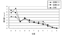
- FIG. 10 is a graph illustrating an example of a measurement result and a simulation result of the amount of displacement of the object to be adsorbed, which is implemented by the present inventor using the AC drive electrostatic chuck according to the present embodiment.
- FIG. 10 is a graph illustrating an example of a measurement result and a simulation result of the amount of displacement of the object to be adsorbed, which is implemented by the present inventor using the AC drive electrostatic chuck according to the present embodiment.
- FIG. 11 is a schematic plan view showing measurement positions and data positions in the measurement results and simulation results shown in FIG.
- FIG. 12 is a graph illustrating an example of a measurement result and a simulation result of the amount of displacement of the object to be adsorbed performed by the present inventor using the AC drive electrostatic chuck according to the comparative example.
- FIG. 13 is a schematic plan view showing measurement positions and data positions in the measurement results and simulation results shown in FIG.
- FIG. 14 is a schematic plan view illustrating another arrangement relationship between the electrodes and the protrusions of this embodiment.
- FIG. 15 is a schematic plan view illustrating still another arrangement relationship between the electrodes and the protrusions of this embodiment.
- FIG. 16 is a schematic plan view illustrating still another arrangement relationship between the electrodes and the protrusions of this embodiment.
- FIG. 17A and FIG. 17B are schematic plan views illustrating still another arrangement relationship between the electrodes and the protrusions of this embodiment.
- FIG. 18A and FIG. 18B are schematic plan views illustrating still another arrangement relationship between the electrodes and the protrusions of this embodiment.
- FIG. 19A and FIG. 19B are schematic plan views illustrating still another arrangement relationship between the electrodes and the protrusions of this embodiment.
- FIG. 20A and FIG. 20B are schematic plan views illustrating still another arrangement relationship between the electrodes and the protrusions of this embodiment.
- FIG. 21 is a schematic plan view illustrating still another arrangement relationship between the electrodes and the protrusions of this embodiment.
- FIG. 22A and FIG. 22B are schematic cross-sectional views in which the protrusions of this embodiment are selectively arranged.
- FIG. 23A and FIG. 23B are schematic cross-sectional views for explaining the diameter of the protrusion.
- FIG. 24 is a schematic plan view illustrating a modification of the electrode pattern of this embodiment.
- FIG. 25 is a schematic plan view illustrating another modification of the electrode pattern of this embodiment.
- FIG. 26 is a schematic plan view illustrating still another modified example of the electrode pattern of this embodiment.
- FIG. 27 is a schematic plan view illustrating still another modified example of the electrode pattern of this embodiment.
- FIG. 28 is a schematic plan view illustrating still another modified example of the electrode pattern of this embodiment.
- FIG. 29 is a schematic plan view illustrating still another modification of the electrode pattern of this embodiment.
- FIG. 30 is a schematic plan view illustrating still another modification of the electrode pattern of this embodiment.
- FIG. 24 is a schematic plan view illustrating a modification of the electrode pattern of this embodiment.
- FIG. 25 is a schematic plan view illustrating another modification of the electrode pattern of this embodiment.
- FIG. 26 is a schematic plan view
- FIG. 31 is a schematic plan view illustrating still another modified example of the electrode pattern of this embodiment.
- FIG. 32 is a schematic plan view illustrating still another modified example of the electrode pattern of the present embodiment.
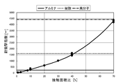
- FIG. 33 is a graph illustrating an example of the relationship between the electrode width and the impact resistance index.
- FIG. 34 is a graph illustrating an example of the relationship between the electrode interval and the impact resistance index.
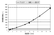
- FIG. 35 is a graph illustrating an example of the relationship between the protrusion pitch and the impact resistance index.
- FIG. 36 is a graph illustrating an example of the relationship between the contact area ratio and the impact resistance index.
- FIG. 37 is a graph illustrating an example of the relationship between the protrusion diameter and the impact resistance index.
- FIG. 38 is a graph illustrating an example of the relationship between the surface roughness of the top surface of the protrusion and the impact resistance index.
- a dielectric substrate having a protrusion formed on the main surface on the side where the object to be adsorbed is placed, and a bottom surface formed around the protrusion, and the dielectric substrate.
- the electrode includes a plurality of electrode elements spaced apart from each other, and AC voltages having different phases can be applied to each of the plurality of electrode elements, and the protrusions
- the unit is an AC driven electrostatic chuck that is arranged on the main surface at predetermined intervals according to the shapes of the plurality of electrode elements.
- the protrusions are arranged on the main surface of the dielectric substrate at predetermined intervals according to the shapes of the plurality of electrode elements, so that the displacement of the object to be attracted is made substantially uniform.
- the vibration can be controlled. Moreover, it can prevent that a part of projection part is damaged locally.
- the AC driven electrostatic chuck according to the first aspect, wherein the protrusions are present on a projection surface obtained by projecting the plurality of electrode elements onto the main surface.
- This AC driven electrostatic chuck can further suppress the vibration of the object to be adsorbed. Moreover, it can prevent that a part of projection part is damaged locally.
- the protrusion is present at a position that is not on a projection plane obtained by projecting the plurality of electrode elements onto the main surface. It is a chuck.
- This AC driven electrostatic chuck can further suppress the vibration of the object to be adsorbed. Moreover, it can prevent that a part of projection part is damaged locally.
- each of the plurality of electrode elements has a portion that extends, and the projection is a projection plane obtained by projecting the plurality of electrode elements onto the main surface.
- the AC driven electrostatic chuck is located above the center line extending in the extending direction of the portion.
- This AC driven electrostatic chuck can further suppress the vibration of the object to be adsorbed. Moreover, it can prevent that a part of projection part is damaged locally.
- the gap provided between the adjacent electrode elements of the plurality of electrode elements has an extending portion, and the protrusion is the gap.
- the AC driven electrostatic chuck is located on a projection plane obtained by projecting the projection on the main surface and not on a center line extending in the extending direction of the portion.
- This AC driven electrostatic chuck can further suppress the vibration of the object to be adsorbed. Moreover, it can prevent that a part of projection part is damaged locally.
- the plurality of protrusions are located symmetrically with respect to the center line on a projection plane obtained by projecting the plurality of electrode elements onto the main surface.
- This is an AC driven electrostatic chuck.
- This AC driven electrostatic chuck can further suppress the vibration of the object to be adsorbed. Moreover, it can prevent that a part of projection part is damaged locally.
- the plurality of protrusions are present at positions symmetrical with respect to the center line on a projection surface obtained by projecting the gap onto the main surface.
- the AC drive electrostatic chuck is characterized.
- This AC driven electrostatic chuck can further suppress the vibration of the object to be adsorbed. Moreover, it can prevent that a part of projection part is damaged locally.
- a gap provided between adjacent electrode elements of the plurality of electrode elements has an extending portion
- the plurality of protrusions are An AC-driven electrostatic chuck characterized in that the plurality of electrode elements are present on a projection surface obtained by projecting the plurality of electrode elements on the main surface at positions symmetrical with respect to a center line extending in the extending direction of the portion. is there.
- This AC driven electrostatic chuck can further suppress the vibration of the object to be adsorbed. Moreover, it can prevent that a part of projection part is damaged locally.
- each of the plurality of electrode elements has an extending portion, and the projection is a projection plane obtained by projecting the plurality of electrode elements onto the main surface.
- the AC driven electrostatic chuck is located on a center line extending in the extending direction of the portion.
- This AC driven electrostatic chuck can prevent local damage to a part of the protrusion.
- the gap provided between the adjacent electrode elements of the plurality of electrode elements has an extending portion, and the protrusion is the gap.
- the AC driven electrostatic chuck is located on a center line extending in the extending direction of the portion on a projection surface obtained by projecting the main surface onto the main surface.
- This AC driven electrostatic chuck can prevent local damage to a part of the protrusion.
- the interval between adjacent protrusions arranged at the center of the main surface is the interval between adjacent protrusions arranged at the outer peripheral portion of the main surface. It is an AC drive electrostatic chuck characterized by being narrower than that.
- the protrusions are denser in the central portion of the main surface of the dielectric substrate than in the outer peripheral portion of the main surface of the dielectric substrate. Therefore, it is possible to prevent a part of the protrusions arranged on the outer peripheral portion of the main surface of the dielectric substrate from being locally damaged.
- the distance between adjacent electrodes disposed in the central portion of the main surface is greater than the distance between adjacent electrodes disposed in the outer peripheral portion of the main surface.
- the electrodes are denser in the central portion of the main surface of the dielectric substrate than in the outer peripheral portion of the main surface of the dielectric substrate. Therefore, the protrusions are denser in the central portion of the main surface of the dielectric substrate than in the outer peripheral portion of the main surface of the dielectric substrate. Therefore, it is possible to prevent a part of the protrusions arranged on the outer peripheral portion of the main surface of the dielectric substrate from being locally damaged.
- the ratio of the area of the top surface of the protruding portion disposed in the central portion to the total area of the main surface when viewed perpendicular to the main surface Is an AC driven electrostatic chuck characterized in that the ratio is higher than the ratio of the area of the top surface of the protrusion disposed on the outer peripheral portion to the entire area of the main surface.
- the contact area of the protrusion disposed at the center of the main surface of the dielectric substrate with the object to be attracted is the protrusion disposed at the outer peripheral portion of the main surface of the dielectric substrate. It is wider than the contact area with the adsorbent. Therefore, it is possible to prevent a part of the protrusions arranged on the outer peripheral portion of the main surface of the dielectric substrate from being locally damaged.
- the diameter of the protrusion disposed on the outer peripheral portion of the main surface is the same as the diameter of the protrusion disposed on the central portion of the main surface.
- An AC-driven electrostatic chuck characterized in that it is larger than the diameter of the protrusion disposed at the center of the main surface.
- this AC driven electrostatic chuck when used in a substrate processing apparatus that performs ion implantation, a beam is irradiated, so that an object to be adsorbed such as a semiconductor wafer may thermally expand.
- an object to be adsorbed such as a semiconductor wafer may thermally expand.
- the protrusion disposed on the outer peripheral portion of the main surface of the dielectric substrate is more easily scraped than the protrusion disposed on the central portion of the main surface of the dielectric substrate.
- the diameter of the protrusion disposed on the outer peripheral portion of the main surface of the dielectric substrate is the same as the diameter of the protrusion disposed on the central portion of the main surface of the dielectric substrate, or the dielectric It is larger than the diameter of the protrusion part arrange
- the projection disposed on the outer peripheral portion of the main surface is disposed at a central portion of the main surface when viewed perpendicular to the main surface. Further, the AC driven electrostatic chuck is arranged at a position selectively moved in the outer circumferential direction with respect to the arrangement pattern of the protrusions.
- the protrusion disposed on the outer peripheral portion of the main surface is disposed at a central portion of the main surface when viewed perpendicular to the main surface. Further, the AC driven electrostatic chuck is arranged at a position selectively moved in the outer circumferential direction with respect to the arrangement pattern of the protrusions.
- the protrusion disposed on the second round from the outermost periphery when viewed perpendicular to the main surface is viewed perpendicular to the main surface.
- An AC-driven electrostatic chuck characterized in that it is arranged at a position that is selectively moved in the outer circumferential direction with respect to the arrangement pattern of the protrusions arranged at positions other than the second circumference from the outermost circumference.
- when the protrusion disposed on the second circumference from the outermost periphery when viewed perpendicular to the main surface is viewed perpendicular to the main surface.
- An AC-driven electrostatic chuck characterized in that it is arranged at a position that is selectively moved in the outer circumferential direction with respect to the arrangement pattern of the protrusions arranged at positions other than the second circumference from the outermost circumference.
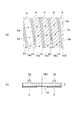
- FIG. 1A to FIG. 1C are schematic cross-sectional views for illustrating an AC drive electrostatic chuck according to an embodiment of the present invention.
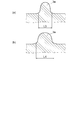
- FIG. 1A is a schematic cross-sectional view for illustrating an AC driven electrostatic chuck.
- FIG.1 (b) is an enlarged schematic diagram of the A section represented to Fig.1 (a).
- FIG.1 (c) is the graph which measured the B section represented to FIG.1 (b) using the contact-type roughness meter.
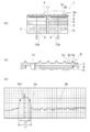
- the AC drive electrostatic chuck 1 includes a base 2, a dielectric substrate 3, and an electrode 4.
- An insulator layer 5 made of an inorganic material is formed on one main surface (surface on the electrode 4 side) of the base 2.
- the dielectric substrate 3 has a protrusion 3a formed on the main surface (mounting surface side) on which the object to be attracted is placed, and a bottom surface 3b formed around the protrusion 3a. is doing.
- the top surface of the projection 3a becomes a mounting surface when an object to be adsorbed such as a semiconductor wafer is mounted.
- the main surface of the dielectric substrate 3 provided with the electrode 4 and the main surface of the base 2 provided with the insulator layer 5 are bonded with an insulating adhesive. A material obtained by curing the insulating adhesive becomes the bonding layer 6.
- the AC driven electrostatic chuck 1 shown in FIG. 1A has a structure in which a dielectric substrate 3 and an insulator layer 5 are joined, which will be described later with reference to FIGS. 2A and 2B.
- the electrode may be built in the dielectric substrate.
- the “top surface” in the present specification will be described. As shown in FIG. 1C, the “top surface” in the specification of the present application refers to a portion that is within the range of the length L2 from the central axis of the protrusion 3a.
- L2 is 80% of the length L1 of the bottom of the protrusion 3a.
- the top surface 3a1 of the protrusion 3a has, for example, a curved surface.
- the outside of the top surface 3a1 may be a curved surface or a linear surface.
- the electrode 4 is connected to the power supply 10a and the power supply 10b by electric wires 9, respectively.
- the electric wire 9 is provided so that the base 2 may be penetrated, the electric wire 9 and the base 2 are insulated.
- An AC-driven electrostatic chuck 1 illustrated in FIGS. 1A to 1C is a so-called bipolar electrostatic chuck formed on a dielectric substrate 3 so that a positive electrode and a negative electrode are adjacent to each other. is there.
- the present invention is not limited to this, and the AC drive electrostatic chuck 1 according to the present embodiment may be a tripolar type or other multipolar type.
- the number, shape, and arrangement of the electrodes can be changed as appropriate. This will be described in detail later.
- a through hole 11 is provided so as to penetrate the AC driven electrostatic chuck 1.
- One end of the through hole 11 opens to the bottom surface portion 3b.
- the other end of the through hole 11 is connected to a gas supply unit (not shown) via a pressure control unit and a flow rate control unit (not shown).
- a gas supply means for cooling gas (not shown) supplies helium gas or argon gas.
- the space 3c provided by forming the bottom face part 3b becomes a passage of the supplied gas. The spaces 3c communicate with each other, and the supplied gas is distributed throughout.
- a ring-shaped protrusion may be disposed at a position for supporting the outer peripheral portion of the object to be adsorbed when the object to be adsorbed such as a semiconductor wafer is placed. Thereby, it can suppress that the gas mentioned above leaks.
- a ring-shaped protrusion may be provided around the through hole. Thereby, it can suppress that the gas mentioned above leaks.
- a radial or concentric gas distribution groove (concave groove) (not shown) communicating with the through hole 11 can be provided in the bottom surface portion 3b. If such a gas distribution groove is provided, the gas distribution speed can be increased.
- the base 2 is made of a metal having high thermal conductivity such as aluminum alloy or copper.
- a flow path 8 through which a cooling liquid or a heating liquid flows is provided inside the base 2.
- the flow path 8 does not necessarily need to be provided, it is preferable that it is provided from the viewpoint of temperature control of the object to be adsorbed.
- the insulator layer 5 provided on one main surface of the base 2 is formed of a polycrystalline material such as alumina (Al 2 O 3 ) or yttria (Y 2 O 3 ).
- the thermal conductivity of the insulator layer 5 is preferably higher than the thermal conductivity of the bonding layer 6.
- the thermal conductivity of the insulator layer 5 is more preferably 2 W / mK or more.
- the thermal conductivity of the bonding layer 6 is preferably higher.
- the thermal conductivity of the bonding layer 6 is preferably 1 W / mK or more, and more preferably 1.6 W / mK or more.
- Such thermal conductivity can be obtained, for example, by adding alumina or aluminum nitride as a filler to silicone or epoxy resin.
- thermal conductivity can also be adjusted with the ratio of addition.
- the thickness of the bonding layer 6 is preferably as thin as possible in consideration of heat transfer properties. On the other hand, considering the fact that the bonding layer 6 peels off due to the thermal shear stress resulting from the difference between the thermal expansion coefficient of the base 2 and the thermal expansion coefficient of the dielectric substrate 3, the thickness of the bonding layer 6 can be as much as possible. A thicker one is preferred. Therefore, the thickness of the bonding layer 6 is preferably 0.1 mm or more and 0.3 mm or less in consideration of these.
- the dielectric substrate 3 is preferably formed of a polycrystalline ceramic sintered body.
- the polycrystalline ceramic sintered body include a polycrystalline ceramic sintered body made of alumina, yttria, aluminum nitride, silicon carbide, or the like.
- the volume resistivity of the material of the dielectric substrate 3 is, for example, 10 8 ⁇ cm or more in the use temperature region of the electrostatic chuck (for example, room temperature (about 25 ° C.)).
- the volume resistivity in this specification is a value measured using the method shown in JIS standard (JIS C 2141: 1992 ceramic material test method for electrical insulation). The measurement in this case can be performed in the operating temperature range of the electrostatic chuck.
- Examples of the material of the electrode 4 include titanium oxide, titanium alone or a mixture of titanium and titanium oxide, titanium nitride, titanium carbide, tungsten, gold, silver, copper, aluminum, chromium, nickel, and a gold-platinum alloy. be able to.
- FIG. 2A and FIG. 2B are schematic cross-sectional views for illustrating modifications of the AC-driven electrostatic chuck according to the present embodiment.
- FIG. 2A is a schematic cross-sectional view for illustrating an AC driven electrostatic chuck.
- FIG. 2B is an enlarged schematic diagram of the F portion shown in FIG.
- the electrode 4 is embedded in the dielectric substrate 30. That is, the electrode 4 is built in the dielectric substrate 30.
- Such an AC drive electrostatic chuck 1a is manufactured using, for example, a green sheet printing lamination method.
- the electrode 4 is formed by screen printing a tungsten paste on a green sheet made of a polycrystalline ceramic molded body (for example, a polycrystalline alumina molded body). Thereafter, a plurality of green sheets are pressure-laminated so as to embed the electrode 4 to form a laminate before firing.
- Dielectric substrate 30 in which electrode 4 is embedded can be manufactured by cutting this laminated body into a desired shape and firing it in a desired atmosphere.
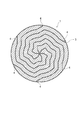
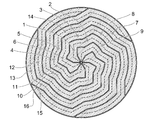
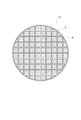
- FIG. 3 is a schematic plan view illustrating the electrode pattern of this embodiment.
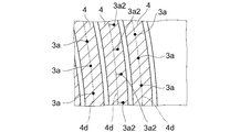
- FIGS. 4A and 4B are schematic plan views illustrating the positional relationship between the electrodes and the protrusions of this embodiment.
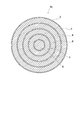
- FIG. 5 is a schematic plan view illustrating the electrode pattern of the AC-driven electrostatic chuck according to the comparative example.
- FIGS. 6A and 6B are schematic plan views illustrating the positional relationship between the electrodes and the protrusions of the AC drive electrostatic chuck according to the comparative example.
- 4A and 6A are schematic plan views showing an AC-driven electrostatic chuck when viewed perpendicularly to the main surface of the dielectric substrate 3.
- FIG. 4B is an enlarged schematic diagram of a C portion shown in FIG.
- FIG. 6B is an enlarged schematic diagram of the D portion shown in FIG.
- the AC drive electrostatic chuck 1 has a plurality of electrodes 4.
- the electrode 4 includes a plurality of electrode elements.
- Each of the plurality of electrode elements is spaced apart from each other. Therefore, as shown in FIG. 4B, there is a portion (gap) 14 where the electrodes 4 are not disposed between the adjacent electrodes 4.
- the plurality of electrode elements are arranged in a substantially spiral shape. AC voltages having different phases can be applied to each of the plurality of electrode elements.
- a 6-pole electrode 4 is provided in the AC drive electrostatic chuck 1 shown in FIGS. 3 and 4A. And the electrode 4 of every 2 poles of 6 poles makes a pair. That is, the six electrodes 4 form three pairs. Therefore, a three-phase AC voltage is applied to the electrode 4 having the pattern shown in FIGS. 3 and 4A. For example, when an arbitrary moment is observed, a positive polarity voltage is applied to the first pair of electrodes 4 (first phase electrodes). A negative polarity voltage is applied to the electrode 4 (second phase electrode) forming the second pair. No voltage is applied to the third pair of electrodes 4 (third phase electrodes). That is, the voltage applied to the third pair of electrodes 4 is zero. Such an application pattern of the three-phase AC voltage is switched over time.
- the electrode 4 when viewed in the direction perpendicular to the direction in which the electrode 4 extends is shown.
- the width (hereinafter referred to as “electrode width” for convenience of description) is wider than the electrode width of the electrode 4 of the AC driven electrostatic chuck 1 shown in FIGS. 3 and 4A.
- the electrode 4 includes a plurality of electrode elements as in the AC driven electrostatic chuck 1 described above with reference to FIGS. 3, 4A, and 4B. Each of the plurality of electrode elements is spaced apart from each other. Therefore, as shown in FIG. 6B, a gap 14 exists between the electrodes 4 adjacent to each other. AC voltages having different phases can be applied to each of the plurality of electrode elements.
- the protrusions 3a are substantially uniformly spaced at substantially equal intervals over the entire dielectric substrate 3.
- the protrusions 3a are arranged at substantially equal intervals without depending on the shape of the plurality of electrode elements or the pattern of the plurality of electrode elements. That is, the protrusions 3a are arranged at substantially equal intervals regardless of the shape of the plurality of electrode elements or the pattern of the plurality of electrode elements.
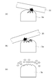
- FIG. 7A and FIG. 7B are schematic plan views for explaining local damage of the protrusions.
- FIGS. 8A to 8C are enlarged schematic views in which the protrusions are enlarged and viewed.
- FIG. 9 is an enlarged schematic view in which the protrusions of the DC drive electrostatic chuck are enlarged.
- FIG. 7A is a schematic plan view illustrating the case where the voltage applied to the second phase electrode 4b is zero.
- FIG. 7B is a schematic plan view illustrating the case where the voltage applied to the third phase electrode 4c is zero.
- the base 2 and the insulator layer 5 are omitted.
- Fig.8 (a) is an enlarged schematic diagram of the E section represented to Fig.7 (a).
- FIG. 8B is an enlarged schematic diagram of the G portion shown in FIG.
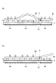
- the action of the object to be attracted in the DC drive electrostatic chuck will be described with reference to FIG.
- the DC drive electrostatic chuck when a DC voltage is applied to the electrodes, the attracted object 20 is attracted and held by the DC drive electrostatic chuck. At this time, the to-be-adsorbed object 20 contacts the protrusion 3a. Subsequently, when the DC voltage applied to the electrode is set to zero, the adsorption force acting on the object to be adsorbed 20 is released, and the object to be adsorbed 20 can be detached from the DC drive electrostatic chuck. Subsequently, the same operation is performed on the other objects to be adsorbed 20. Therefore, as shown by the arrows in FIG.
- an AC driven electrostatic chuck may be used to improve the adsorption / desorption response.
- FIG. 7A for example, at any moment when a voltage is applied to the first phase electrode 4a and the third phase electrode 4c and no voltage is applied to the second phase electrode 4b, the first phase The portion of the object to be attracted 20 positioned on the electrode 4a and the third phase electrode 4c is attracted and held by the AC driven electrostatic chuck 1 by an attracting force. At this time, the portion of the object to be adsorbed 20 located on the first phase electrode 4a and the third phase electrode 4c is in contact with the protruding portion 3a.
- the portion of the object to be adsorbed 20 positioned on the second phase electrode 4b Adsorption force does not work. Therefore, the portion of the object to be adsorbed 20 located on the second phase electrode 4b is lifted from the top surface (contact surface) of the protrusion 3a due to the influence of the supply gas, and is displaced in a direction away from the protrusion 3a. At this time, as shown in FIG. 8A, the protrusion 3 a and the object to be adsorbed 20 may be locally rubbed to damage the protrusion 3 a.
- the application pattern of the three-phase AC voltage is switched over time.
- FIG. 7B for example, at any moment when a voltage is applied to the first phase electrode 4a and the second phase electrode 4b and no voltage is applied to the third phase electrode 4c,
- the portion of the object to be attracted 20 positioned on the first phase electrode 4a and the second phase electrode 4b is attracted and held by the AC drive electrostatic chuck 1 by the attraction force.
- the portion of the object to be adsorbed 20 located on the first phase electrode 4a and the second phase electrode 4b is in contact with the protrusion 3a.
- the portion of the adsorbent 20 located on the third phase electrode 4c Adsorption force does not work. Therefore, the portion of the object to be adsorbed 20 located on the third phase electrode 4c is lifted from the top surface of the protrusion 3a and displaced in a direction away from the protrusion 3a.
- the protrusion 3a and the object to be adsorbed are different from the part where the protrusion 3a and the object to be adsorbed 20 described above with reference to FIG. 20 rubs locally. As a result, the protrusion 3a may be damaged at a place different from the place where the protrusion 3a described above with reference to FIG.
- the application pattern of the three-phase AC voltage is sequentially switched over time, and when the state described above with reference to FIG. 8A and the state described above with reference to FIG. May be partially damaged. Then, as shown in FIG. 8C, a part of the locally damaged protrusion 3a may be broken and particles may be generated. That is, if not only the collision between the object to be adsorbed 20 and the protrusion 3a but also the friction between the object to be adsorbed 20 and the protrusion 3a repeatedly, a part of the protrusion 3a may be locally damaged and damaged. is there.
- the protrusion 3a has a plurality of electrode element shapes or a plurality of electrode element patterns. Are arranged at predetermined intervals. “According to the shape of a plurality of electrode elements or the pattern of a plurality of electrode elements” means, for example, “reflecting the shape of a plurality of electrode elements or the pattern of a plurality of electrode elements”, “the shape of a plurality of electrode elements Or along the pattern of a plurality of electrode elements ”,“ follow the shape of a plurality of electrode elements or the pattern of a plurality of electrode elements ”,“ Match the shape of a plurality of electrode elements or the pattern of a plurality of electrode elements ” And “based on the shape of the plurality of electrode elements or the pattern of the plurality of electrode elements”. These will be described later with specific examples.
- the protrusion 3 a is present on a projection surface obtained by projecting a plurality of electrode elements onto the main surface of the dielectric substrate 3. Moreover, as illustrated in FIG. 4B, each of the plurality of electrode elements has an extending portion.
- the protrusion 3a has a center line 4d (hereinafter, for convenience of description) extending in a direction in which each portion of the plurality of electrode elements extends on a projection surface obtained by projecting the plurality of electrode elements onto the main surface of the dielectric substrate 3. On the electrode center line).
- the displacement amount of the to-be-adsorbed object 20 can further be suppressed.
- the distance between adjacent electrodes 4 arranged at the center of the main surface of the dielectric substrate 3. is narrower than the distance between adjacent electrodes 4 arranged on the outer peripheral portion of the main surface of the dielectric substrate 3.
- the electrode width of the electrode 4 disposed at the center of the main surface of the dielectric substrate 3 is narrower than the electrode width of the electrode 4 disposed at the outer peripheral portion of the main surface of the dielectric substrate 3. That is, the electrodes 4 are denser in the central portion of the main surface of the dielectric substrate 3 than in the outer peripheral portion of the main surface of the dielectric substrate 3.
- the interval between the adjacent protrusions 3 a arranged at the center of the main surface of the dielectric substrate 3 is the same as that of the main surface of the dielectric substrate 3. It is narrower than the interval between adjacent protrusions 3a arranged on the outer periphery. That is, the protrusions 3 a are denser in the central portion of the main surface of the dielectric substrate 3 than in the outer peripheral portion of the main surface of the dielectric substrate 3. Therefore, when viewed perpendicularly to the main surface of the dielectric substrate 3, the ratio of the area of the top surface of the protrusion 3a disposed at the center to the area of the entire main surface of the dielectric substrate 3 is the dielectric substrate.
- the contact area (top surface area) of the protrusion 3a arranged at the center of the main surface of the dielectric substrate 3 with the object to be adsorbed 20 is the dielectric substrate.
- 3 is wider than the contact area (the area of the top surface) of the protrusion 3a arranged on the outer peripheral portion of the main surface 3 with the object 20 to be adsorbed.
- the area of the top surface of the protrusion 3a is the ring-shaped protrusion. It includes the area of the top surface.
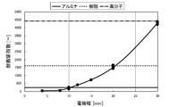
- FIG. 10 is a graph illustrating an example of a measurement result and a simulation result of the amount of displacement of the object to be adsorbed, which is implemented by the present inventor using the AC drive electrostatic chuck according to the present embodiment.
- FIG. 11 is a schematic plan view showing measurement positions and data positions in the measurement results and simulation results shown in FIG.
- FIG. 12 is a graph illustrating an example of a measurement result and a simulation result of the amount of displacement of the object to be adsorbed performed by the present inventor using the AC drive electrostatic chuck according to the comparative example.
- FIG. 13 is a schematic plan view showing measurement positions and data positions in the measurement results and simulation results shown in FIG.
- the horizontal axis of the graph shown in FIG. 12 represents the measurement position and the read data position.
- the vertical axis of the graph shown in FIG. 12 represents the amount of displacement of the object to be adsorbed 20.
- the pressure of the gas supplied to the space 3c was set to 20 Torr. .
- the measurement position and the read data position are as shown in FIG.
- the displacement amount of the adsorbed object 20 at the positions a and b among the positions a to k is larger than the displacement amounts at other positions.
- the amount of displacement of the attracted object 20 at the position a and the position b is about 6 micrometers ( ⁇ m) to 7 ⁇ m.
- the amount of displacement of the attracted object 20 at the position a and the position b is about 4 ⁇ m to 5 ⁇ m.
- the displacement amount of the adsorbed object 20 at the position j and the position k among the positions a to k is smaller than the displacement amount at the other positions.
- the position j and the position k are positions where the electrode width of the electrode 4 is narrower than other positions. Thereby, when the electrode width of the electrode 4 is made narrower, it can be seen that the amount of displacement of the adsorbent 20 can be made smaller.
- the horizontal axis of the graph shown in FIG. 10 represents the measurement position and the read data position.
- the vertical axis of the graph shown in FIG. 10 represents the amount of displacement of the object to be adsorbed 20.
- the amount of displacement of the adsorbed object 20 at all positions 1 to 16 was about 0.2 ⁇ m or less in both actual measurement and simulation. That is, it was found that the displacement amount of the object to be attracted 20 can be suppressed in the AC driven electrostatic chuck according to the present embodiment.
- FIG. 14 is a schematic plan view illustrating another arrangement relationship between the electrodes and the protrusions of this embodiment. Note that FIG. 14 corresponds to an enlarged schematic diagram of a C portion illustrated in FIG.
- the protrusion 3 a exists at a position that is not on the projection surface obtained by projecting the plurality of electrode elements onto the main surface of the dielectric substrate 3. That is, the protrusion 3 a exists on the gap 14 when the electrode 4 is projected onto the main surface of the dielectric substrate 3. Further, as illustrated in FIG. 14, the gap 14 has an extending portion.
- the protrusion 3 a has a center line 14 d (hereinafter referred to as “gap center line” for convenience of explanation) extending in a direction in which the portion of the gap 14 extends on the projection surface obtained by projecting the gap 14 onto the main surface of the dielectric substrate 3. Exist). Thereby, the displacement amount of the to-be-adsorbed object 20 can further be suppressed. Moreover, it is possible to prevent a part of the protrusion 3a from being locally damaged.
- FIG. 15 is a schematic plan view illustrating still another arrangement relationship between the electrodes and the protrusions of this embodiment. Note that FIG. 15 corresponds to an enlarged schematic diagram of a C portion illustrated in FIG.
- the protrusion 3 a exists on a projection surface obtained by projecting a plurality of electrode elements onto the main surface of the dielectric substrate 3.
- the protrusion 3 a is present at a position that is not on the center line 4 d of the electrode 4 on the projection surface obtained by projecting a plurality of electrode elements onto the main surface of the dielectric substrate 3.
- the protrusion 3 a is present at a position intermediate between the center line 4 d of the electrode 4 and the end 4 e of the electrode 4 on the projection surface obtained by projecting a plurality of electrode elements onto the main surface of the dielectric substrate 3.
- the position of the protrusion 3a is not limited to this.
- the protrusion 3 a is located on a projection plane obtained by projecting a plurality of electrode elements onto the main surface of the dielectric substrate 3 and not on the center line 4 d of the electrode 4, and is separated from the center line 4 d of the electrode 4 by a predetermined distance. It suffices if it exists at a certain position.
- the arrangement period of the protrusions 3 a exists at a position that is an integral multiple of the arrangement period of the pattern of the electrodes 4. Thereby, the displacement amount of the to-be-adsorbed object 20 can further be suppressed.
- FIG. 16 is a schematic plan view illustrating still another arrangement relationship between the electrodes and the protrusions of this embodiment. Note that FIG. 16 corresponds to an enlarged schematic diagram of a C portion illustrated in FIG.
- the protrusion 3 a is present at a position that is not on the projection surface obtained by projecting the plurality of electrode elements onto the main surface of the dielectric substrate 3.
- the protrusion 3 a is present at a position not on the center line 14 d of the gap 14 on the projection surface obtained by projecting the gap 14 onto the main surface of the dielectric substrate 3.
- the protrusion 3 a is present at an intermediate position between the center line 14 d of the gap 14 and the end 14 e of the gap 14 on the projection surface obtained by projecting the gap 14 onto the main surface of the dielectric substrate 3.
- the position of the protrusion 3a is not limited to this.
- the protrusion 3a is located on a projection plane obtained by projecting the gap 14 onto the main surface of the dielectric substrate 3 and not on the center line 14d of the gap 14 and a position separated from the center line 14d of the gap 14 by a predetermined distance. It only has to exist. In other words, it suffices if the arrangement period of the protrusions 3 a exists at a position that is an integral multiple of the arrangement period of the pattern of the gap 14. Thereby, the displacement amount of the to-be-adsorbed object 20 can further be suppressed.
- FIG. 17A and FIG. 17B are schematic plan views illustrating still another arrangement relationship between the electrodes and the protrusions of this embodiment. Note that FIG. 17A corresponds to an enlarged schematic diagram of a C portion illustrated in FIG. FIG. 17B is a schematic cross-sectional view taken along the cutting plane AA shown in FIG.
- the plurality of protrusions 3a are present on a projection surface obtained by projecting a plurality of electrode elements onto the main surface of the dielectric substrate 3.
- FIG. The plurality of protrusions 3 a are present at positions that are not on the center line 4 d of the electrode 4 on the projection surface obtained by projecting the plurality of electrode elements onto the main surface of the dielectric substrate 3.
- the plurality of protrusions 3 a are present at positions symmetrical with respect to the center line 4 d of the electrode 4 on the projection surface obtained by projecting the plurality of electrode elements onto the main surface of the dielectric substrate 3.
- the positions of the plurality of protrusions 3a are not limited to the positions shown in FIGS. 17A and 17B (for example, the position of the end 4e of the electrode 4).
- the plurality of protrusions 3 a are located symmetrically with respect to the center line 4 d of the electrode 4 on the projection surface obtained by projecting the plurality of electrode elements onto the main surface of the dielectric substrate 3, Instead of the position of the end 4 e, it may exist at a position intermediate between the center line 4 d of the electrode 4 and the end 4 e of the electrode 4. Thereby, the displacement amount of the to-be-adsorbed object 20 can further be suppressed.
- FIG. 18A and FIG. 18B are schematic plan views illustrating still another arrangement relationship between the electrodes and the protrusions of this embodiment. Note that FIG. 18A corresponds to an enlarged schematic view of a C portion illustrated in FIG. FIG. 18B is a schematic cross-sectional view taken along the cutting plane BB shown in FIG.
- the plurality of protrusions 3a are present on a projection surface obtained by projecting a plurality of electrode elements onto the main surface of the dielectric substrate 3.
- the plurality of protrusions 3 a are present at positions symmetrical with respect to the center line 14 d of the gap 14 on the projection surface obtained by projecting the plurality of electrode elements onto the main surface of the dielectric substrate 3.
- the positions of the plurality of protrusions 3a are not limited to the positions shown in FIGS. 18A and 18B (for example, the position of the center line 4d of the electrode 4). Thereby, the displacement amount of the to-be-adsorbed object 20 can further be suppressed.
- FIG. 19A and FIG. 19B are schematic plan views illustrating still another arrangement relationship between the electrodes and the protrusions of this embodiment. Note that FIG. 19A corresponds to an enlarged schematic diagram of a C portion illustrated in FIG. FIG. 19B is a schematic cross-sectional view taken along the section CC shown in FIG.
- the plurality of protrusions 3a exist at positions that are not on the projection surface obtained by projecting the plurality of electrode elements onto the main surface of the dielectric substrate 3. In the arrangement relationship shown in FIG.
- the plurality of protrusions 3 a are present at positions symmetrical with respect to the center line 14 d of the gap 14 on the projection surface obtained by projecting the gap 14 onto the main surface of the dielectric substrate 3.
- the positions of the plurality of protrusions 3a are not limited to the middle position between the center line 14d of the gap 14 and the end 14e of the gap 14 (see FIG. 16). Thereby, the displacement amount of the to-be-adsorbed object 20 can further be suppressed.
- the protrusions 3a having the arrangement relationship described above with reference to FIGS. 18 (a) and 18 (b) and the protrusions 3a having the arrangement relationship described above with reference to FIGS. 19 (a) and 19 (b) are: It may be mixed. That is, the plurality of protrusions 3 a are formed on the gap 14 on the projection surface obtained by projecting the plurality of electrode elements on the principal surface of the dielectric substrate 3 and on the projection surface obtained by projecting the gap 14 on the principal surface of the dielectric substrate 3. It may exist in a symmetrical position with respect to the center line 14d.
- FIG. 20A and FIG. 20B are schematic plan views illustrating still another arrangement relationship between the electrodes and the protrusions of this embodiment. Note that FIG. 20A corresponds to an enlarged schematic diagram of a C portion illustrated in FIG. FIG. 20B is a schematic cross-sectional view taken along the section line DD shown in FIG.
- the plurality of protrusions 3a are present on a projection surface obtained by projecting a plurality of electrode elements onto the main surface of the dielectric substrate 3. In the arrangement relationship shown in FIG.
- the plurality of protrusions 3a are formed on the projection surface obtained by projecting the plurality of electrode elements onto the main surface of the dielectric substrate 3, and the plurality of electrodes 4 (five electrodes in FIGS. 20A and 20B). 4) is located symmetrically with respect to the center line 4d of one of the electrodes 4.
- the plurality of protrusions 3 a may not necessarily exist on the projection surface obtained by projecting the plurality of electrode elements onto the main surface of the dielectric substrate 3. That is, if the plurality of protrusions 3 a are present at symmetrical positions with respect to the center line 4 d of one of the plurality of electrodes 4, the plurality of electrode elements are projected onto the main surface of the dielectric substrate 3. It may be present on the gap 14 at the time. Thereby, the displacement amount of the to-be-adsorbed object 20 can further be suppressed.
- FIG. 21 is a schematic plan view illustrating still another arrangement relationship between the electrodes and the protrusions of this embodiment.
- FIGS. 22A and 22B are schematic cross-sectional views in which the protrusions of this embodiment are selectively arranged. Note that FIG. 21 corresponds to an enlarged schematic diagram of a C portion illustrated in FIG.
- FIG. 22A is a schematic cross-sectional view illustrating a case where the protruding portion exists on the center line 4 d of the electrode 4.
- FIG. 22B is a schematic cross-sectional view illustrating a case where the protrusions arranged on the second circumference from the outermost circumference are arranged at positions selectively moved in the outer circumference direction from the center line 4 d of the electrode 4. .
- the protrusion 3 a that has received relatively large damage is the protrusion 3 a that is disposed on the second periphery from the outermost periphery when viewed perpendicular to the main surface of the dielectric substrate 3. It was found that it is contained in a relatively large amount. Further, as described above with reference to FIGS. 7 (a) to 8 (c), when the application pattern of the three-phase AC voltage is switched over time, the object 20 to be adsorbed locally from the protrusion 3a. It vibrates such as floating or coming into contact with the protrusion 3a. As a result of the study by the present inventor, it was found that the amount of displacement of the object to be adsorbed 20 is larger in the outer peripheral portion when viewed perpendicularly to the main surface of the dielectric substrate 3.
- the protrusion 3 a exists on the center line 4 d of the electrode 4 on the projection surface obtained by projecting a plurality of electrode elements onto the main surface of the dielectric substrate 3.
- the first phase electrode 4 a shown in FIG. 22A is assumed to be the electrode 4 arranged on the outermost periphery when viewed perpendicularly to the main surface of the dielectric substrate 3.
- the AC-driven electrostatic chuck shown in FIG. 22A shows the AC-driven electrostatic chuck shown in FIG.
- a plurality of electrode elements are arranged on the projection surface obtained by projecting the principal surface of the dielectric substrate 3 except for the second round from the outermost circumference.
- the projected portion 3 a is present on the center line 4 d of the electrode 4.
- the protrusion 3 a arranged in the second round from the outermost circumference is arranged at a position selectively moved in the outer circumferential direction from the center line 4 d of the electrode 4.
- the first phase electrode 4 a shown in FIG. 22B is assumed to be the electrode 4 arranged on the outermost periphery when viewed perpendicularly to the main surface of the dielectric substrate 3.
- FIG. 22A and FIG. As indicated by the broken line, the object to be adsorbed 20 starts from the protruding portion 3a on the electrode 4 (second phase electrode 4b in FIGS. 22A and 22B) from the outermost circumference to the second circumference. Deform.
- the protruding portion 3a arranged on the second circumference from the outermost circumference is closer to the outer circumference than the center line 4d of the electrode 4 (second phase electrode 4b).
- the displacement amount h2 of the object to be adsorbed 20 shown in FIG. 22B is smaller than the displacement amount h1 of the object to be adsorbed 20 shown in FIG. . Therefore, in order to reduce the displacement amount of the outer peripheral part of the to-be-adsorbed object 20, it is more preferable that the protrusion part 3a arrange
- the protrusions 3a in the vicinity of the outer peripheral portion of the main surface of the dielectric substrate 3 selectively move in the outer peripheral direction with respect to the arrangement pattern of the other protrusions 3a. It is arranged at the position.
- the protrusion 3 a arranged on the other side of the outermost circumference other than the second circumference when viewed perpendicular to the main surface of the dielectric substrate 3 exists on the center line 4 d of the electrode 4.
- the protrusion 3 a 2 disposed on the second circumference from the outermost circumference is at a position selectively moved in the outer circumference direction from the center line 4 d of the electrode 4.
- the object to be adsorbed 20 positioned on the protrusion 3a2 disposed on the second circumference from the outermost circumference when viewed perpendicular to the main surface of the dielectric substrate 3 is obtained. It was found that the displacement of this part can be suppressed. Therefore, it is possible to reduce the singular points where the protrusions 3a and 3a2 are partly damaged locally.
- FIG. 23 (a) and FIG. 23 (b) are schematic cross-sectional views for explaining the diameter of the protrusion.
- FIG. 23 (a) is a schematic cross-sectional view showing a protrusion disposed at the center of the main surface of the dielectric substrate.
- FIG. 23B is a schematic cross-sectional view showing protrusions arranged on the outer peripheral portion of the main surface of the dielectric substrate.
- the object 20 such as a semiconductor wafer may thermally expand because the beam is irradiated.
- the protrusion 3 a disposed on the outer peripheral portion of the main surface of the dielectric substrate 3 is disposed at the center of the main surface of the dielectric substrate 3. It turned out that it is easy to cut rather than the protrusion part 3a.
- the diameter L4 is larger than the diameter L3 of the protrusion 3a arranged at the center of the main surface of the dielectric substrate 3.
- the diameter L4 of the protrusion 3a disposed on the outer peripheral portion of the main surface of the dielectric substrate 3 is substantially the same as the diameter L3 of the protrusion 3a disposed on the central portion of the main surface of the dielectric substrate 3. That is, the diameter of the protrusion 3 a is substantially the same over the entire main surface of the dielectric substrate 3.
- the diameter of the protrusion 3a is a circle equivalent diameter.
- the “equivalent circle diameter” means a circle having the same area as the area of the target planar shape, and means the diameter of the circle.
- the equivalent circle diameter is the diameter of a circle having the same area as the area of the polygon. means.
- FIG. 24 is a schematic plan view illustrating a modification of the electrode pattern of this embodiment.
- FIG. 24 is a schematic plan view showing an AC-driven electrostatic chuck as viewed perpendicularly to the main surface of the dielectric substrate 3. The same applies to the modifications described later with reference to FIGS.
- the electrode 4 of the AC drive electrostatic chuck 1c according to this modification has a fan shape. And the electrode 4 which exhibits a fan shape is arrange
- FIG. 25 is a schematic plan view illustrating another modification of the electrode pattern of this embodiment.
- the electrode 4 of the AC drive electrostatic chuck 1d according to this modification has a triangular shape.
- the electrode 4 disposed on the outer peripheral portion of the main surface of the dielectric substrate 3 is not a triangle, but has a shape in which one side of the triangle follows the shape of the outer periphery of the dielectric substrate 3.
- the electrodes 4 are arranged substantially uniformly over the entire main surface of the dielectric substrate 3.
- FIG. 26 is a schematic plan view illustrating still another modified example of the electrode pattern of this embodiment.
- the electrode 4 of the AC drive electrostatic chuck 1e according to this modification has a quadrangular shape.
- the electrode 4 disposed on the outer peripheral portion of the main surface of the dielectric substrate 3 is not a quadrangle, but has a shape in which one side of the quadrangle or the triangle follows the shape of the outer periphery of the dielectric substrate 3.
- the electrodes 4 are arranged substantially uniformly over the entire main surface of the dielectric substrate 3.
- FIG. 27 is a schematic plan view illustrating still another modified example of the electrode pattern of this embodiment.
- the electrode 4 of the AC-driven electrostatic chuck 1f according to this modification has a partial fan shape.
- a plurality of electrodes 4 in the sector 4f represented by a two-dot chain line form one group.
- the sectors 4f formed by a plurality of electrodes 4 are arranged substantially uniformly in the circumferential direction.
- FIG. 28 is a schematic plan view illustrating still another modified example of the electrode pattern of this embodiment.
- the electrode 4 of the AC driven electrostatic chuck 1g according to the present modification has a hexagonal shape.
- the electrodes 4 are arranged in a honeycomb shape, for example, over the entire main surface of the dielectric substrate 3.
- FIG. 29 is a schematic plan view illustrating still another modification of the electrode pattern of this embodiment.
- the electrode 4 of the AC drive electrostatic chuck 1h according to the present modification includes a plurality of electrode elements.
- the plurality of electrode elements are arranged in a substantially spiral shape.
- a 6-pole electrode 4 is provided in the AC driven electrostatic chuck 1h according to this modification.
- the electrode 4 of every 2 poles of 6 poles makes a pair. That is, the six electrodes 4 form three pairs. Therefore, a three-phase AC voltage is applied to the electrode 4 of the AC driven electrostatic chuck 1h according to this modification.
- FIG. 30 is a schematic plan view illustrating still another modification of the electrode pattern of this embodiment.
- the electrode 4 of the AC drive electrostatic chuck 1i according to the present modification includes a plurality of electrode elements.
- the plurality of electrode elements are arranged substantially concentrically.
- a 6-pole electrode 4 is provided in the AC drive electrostatic chuck 1 i according to this modification.
- the electrode 4 of every 2 poles of 6 poles makes a pair. That is, the six electrodes 4 form three pairs. Therefore, a three-phase AC voltage is applied to the electrode 4 of the AC driven electrostatic chuck 1i according to this modification.
- FIG. 31 is a schematic plan view illustrating still another modified example of the electrode pattern of this embodiment.
- the electrode 4 of the alternating current drive electrostatic chuck 1j according to this modification has a comb shape.
- a 6-pole electrode 4 is provided in the AC drive electrostatic chuck 1j according to this modification.
- the electrode 4 of every 2 poles of 6 poles makes a pair.
- the electrode 4 which makes a pair is arrange
- the six electrodes 4 form three pairs. Therefore, a three-phase AC voltage is applied to the electrode 4 of the AC driven electrostatic chuck 1i according to this modification.
- FIG. 32 is a schematic plan view illustrating still another modified example of the electrode pattern of the present embodiment.
- the electrode 4 of the AC drive electrostatic chuck 1k according to the present modification includes a plurality of electrode elements. The plurality of electrode elements are arranged concentrically. In the AC driven electrostatic chuck 1k according to this modification, a five-pole electrode 4 is provided.
- FIG. 33 is a graph illustrating an example of the relationship between the electrode width and the impact resistance index.
- the horizontal axis shown in FIG. 33 represents the electrode width of the electrode 4.
- the vertical axis shown in FIG. 33 represents the impact resistance index of the dielectric substrate 3.
- impact resistance index is defined as “tensile strength (tensile strength) / impact stress (impact value)”.
- the object 20 is locally displaced or vibrated by the application pattern of the AC voltage. Thereby, the projection part 3a may be damaged.
- the degree to which the protrusion 3a is damaged depends on, for example, the material of the dielectric substrate 3.
- the dielectric substrate 3 is formed of, for example, a polycrystalline ceramic sintered body.
- the polycrystalline ceramic sintered body include a polycrystalline ceramic sintered body made of alumina, yttria, aluminum nitride, silicon carbide, or the like.
- the material of the dielectric substrate 3 is not limited thereto, and may be a polymer compound such as silicon rubber, or a resin such as polyimide (PI). Therefore, the present inventor has defined the above-described impact resistance index in order to unify and express the numerical values specific to the material of the dielectric substrate 3.
- the impact on the dielectric substrate 3 is preferably smaller. Therefore, the lower impact resistance index is preferable.
- the electrode width of the electrode 4 is preferably about 30 mm or less in consideration of the impact resistance index of the polymer compound. In consideration of the impact resistance index of the resin, the electrode width of the electrode 4 is preferably about 20 mm or less. In view of the impact resistance index of alumina, the electrode width of the electrode 4 is more preferably about 10 mm or less. According to these, it is possible to prevent a part of the protrusion 3a from being locally damaged.
- FIG. 34 is a graph illustrating an example of the relationship between the electrode interval and the impact resistance index.
- the horizontal axis shown in FIG. 34 represents the interval between adjacent electrodes 4.
- the interval between adjacent electrodes 4 is the width of the gap 14 when viewed in the direction perpendicular to the direction in which the gap 14 extends.
- the vertical axis shown in FIG. 34 represents the impact resistance index of the dielectric substrate 3. The impact resistance index is as described above with reference to FIG.
- the interval between the adjacent electrodes 4 is preferably about 10 mm or less. Further, considering the impact resistance index of the resin, the interval between adjacent electrodes 4 is more preferably about 6 mm or less. In consideration of the impact resistance index of alumina, the distance between adjacent electrodes 4 is more preferably about 2 mm or less. According to these, it is possible to prevent a part of the protrusion 3a from being locally damaged.
- FIG. 35 is a graph illustrating an example of the relationship between the protrusion pitch and the impact resistance index.
- the horizontal axis shown in FIG. 35 represents the distance (dot pitch) between the centers of adjacent protrusions 3a.
- the vertical axis shown in FIG. 35 represents the impact resistance index of the dielectric substrate 3. The impact resistance index is as described above with reference to FIG.
- the distance between the centers of the adjacent protrusions 3a is preferably about 30 mm or less.
- the distance between the centers of the adjacent protrusions 3a is more preferably about 20 mm or less.
- the thickness is more preferably about 10 mm or less. According to these, it is possible to prevent a part of the protrusion 3a from being locally damaged.
- FIG. 36 is a graph illustrating an example of the relationship between the contact area ratio and the impact resistance index.
- the horizontal axis shown in FIG. 36 represents the ratio of the area of the top surface of the protrusion 3a to the area of the entire main surface of the dielectric substrate 3 (contact area ratio) when viewed perpendicular to the main surface of the dielectric substrate 3. Represents.
- the area of the top surface of the protrusion 3a is the ring-shaped protrusion. It includes the area of the top surface.
- the vertical axis shown in FIG. 36 represents the impact resistance index of the dielectric substrate 3. The impact resistance index is as described above with reference to FIG.
- the contact area ratio is preferably about 70 percent (%) or less. In consideration of the impact resistance index of the resin, the contact area ratio is more preferably about 50% or less. In view of the impact resistance index of alumina, the contact area ratio is more preferably about 10% or less. According to these, it is possible to prevent a part of the protrusion 3a from being locally damaged.
- FIG. 37 is a graph illustrating an example of the relationship between the protrusion diameter and the impact resistance index.
- the horizontal axis shown in FIG. 37 represents the diameter of the protrusion 3a.
- the vertical axis shown in FIG. 37 represents the impact resistance index of the dielectric substrate 3. The impact resistance index is as described above with reference to FIG.
- the diameter of the protruding portion 3a refers to a circle-equivalent diameter.
- the “equivalent circle diameter” is as described above with reference to FIGS. 23 (a) and 23 (b).
- the diameter of the protrusion 3a is preferably about ⁇ 20 mm or less.
- the diameter of the protrusion 3a is more preferably about ⁇ 10 mm or less.
- the diameter of the protrusion 3a is more preferably about ⁇ 2 mm or less. According to these, it is possible to prevent a part of the protrusion 3a from being locally damaged.
- FIG. 38 is a graph illustrating an example of the relationship between the surface roughness of the top surface of the protrusion and the impact resistance index.
- the horizontal axis shown in FIG. 38 represents the arithmetic average roughness Ra of the top surface of the protrusion 3a.
- the top surface of the protrusion 3a is the top of the ring-shaped protrusion. Including the surface.
- the vertical axis shown in FIG. 38 represents the impact resistance index of the dielectric substrate 3. The impact resistance index is as described above with reference to FIG.
- the arithmetic average roughness Ra of the top surface of the protrusion 3a is preferably about 1 ⁇ m or less.
- the arithmetic average roughness Ra of the top surface of the protrusion 3a is more preferably about 0.7 ⁇ m or less.
- the arithmetic average roughness Ra of the top surface of the protrusion 3a is more preferably about 0.3 ⁇ m or less. According to these, it is possible to prevent a part of the protrusion 3a from being locally damaged.
- the present invention has been described above. However, the present invention is not limited to these descriptions. As long as the features of the present invention are provided, those skilled in the art appropriately modified the design of the above-described embodiments are also included in the scope of the present invention.
- the shape, dimensions, material, arrangement, etc. of each element included in the AC drive electrostatic chuck 1 and the like and the installation form of the protrusions 3a and the electrodes 4 are not limited to those illustrated, but may be changed as appropriate. it can.
- examples of the waveform of the AC voltage applied to the electrode 4 include a sine wave and a rectangular wave, but are not limited thereto.
- the effective value, amplitude, and phase of the AC voltage applied to the electrode 4 are not particularly limited.
- Examples of the frequency of the AC voltage applied to the electrode 4 include about 0.1 hertz (Hz) to about 500 Hz, but are not limited thereto.
- Hz hertz
- each element with which each embodiment mentioned above is provided can be combined as long as technically possible, and the combination of these is also included in the scope of the present invention as long as it includes the features of the present invention.
- an AC driven electrostatic chuck capable of suppressing local damage to a part of the protrusion provided on the mounting surface side.
Landscapes
- Engineering & Computer Science (AREA)
- Physics & Mathematics (AREA)
- Condensed Matter Physics & Semiconductors (AREA)
- General Physics & Mathematics (AREA)
- Manufacturing & Machinery (AREA)
- Computer Hardware Design (AREA)
- Microelectronics & Electronic Packaging (AREA)
- Power Engineering (AREA)
- Container, Conveyance, Adherence, Positioning, Of Wafer (AREA)
- Jigs For Machine Tools (AREA)
Priority Applications (3)
| Application Number | Priority Date | Filing Date | Title |
|---|---|---|---|
| CN201280046775.1A CN103890927A (zh) | 2011-09-30 | 2012-09-27 | 交流驱动静电吸盘 |
| KR1020147006021A KR101429593B1 (ko) | 2011-09-30 | 2012-09-27 | 교류구동 정전 척 |
| US14/344,736 US9093488B2 (en) | 2011-09-30 | 2012-09-27 | AC-driven electrostatic chuck |
Applications Claiming Priority (4)
| Application Number | Priority Date | Filing Date | Title |
|---|---|---|---|
| JP2011217622 | 2011-09-30 | ||
| JP2011-217622 | 2011-09-30 | ||
| JP2012-207606 | 2012-09-20 | ||
| JP2012207606A JP5505667B2 (ja) | 2011-09-30 | 2012-09-20 | 交流駆動静電チャック |
Publications (1)
| Publication Number | Publication Date |
|---|---|
| WO2013047647A1 true WO2013047647A1 (ja) | 2013-04-04 |
Family
ID=47995675
Family Applications (1)
| Application Number | Title | Priority Date | Filing Date |
|---|---|---|---|
| PCT/JP2012/074866 WO2013047647A1 (ja) | 2011-09-30 | 2012-09-27 | 交流駆動静電チャック |
Country Status (6)
Cited By (1)
| Publication number | Priority date | Publication date | Assignee | Title |
|---|---|---|---|---|
| JPWO2016159342A1 (ja) * | 2015-04-02 | 2018-01-11 | 株式会社アルバック | 吸着装置、吸着装置の製造方法、及び真空処理装置 |
Families Citing this family (22)
| Publication number | Priority date | Publication date | Assignee | Title |
|---|---|---|---|---|
| JP6224428B2 (ja) | 2013-11-19 | 2017-11-01 | 東京エレクトロン株式会社 | 載置台にフォーカスリングを吸着する方法 |
| US9633885B2 (en) * | 2014-02-12 | 2017-04-25 | Axcelis Technologies, Inc. | Variable electrode pattern for versatile electrostatic clamp operation |
| JP6469985B2 (ja) * | 2014-07-28 | 2019-02-13 | 株式会社日立ハイテクノロジーズ | プラズマ処理装置 |
| KR102174964B1 (ko) * | 2014-09-30 | 2020-11-05 | 스미토모 오사카 세멘토 가부시키가이샤 | 정전 척 장치 |
| CN107636820B (zh) * | 2015-06-04 | 2022-01-07 | 应用材料公司 | 透明静电载具 |
| KR102203402B1 (ko) * | 2016-02-10 | 2021-01-15 | 엔테그리스, 아이엔씨. | 입자 성능이 개선된 웨이퍼 접촉 표면 돌출 프로파일 |
| CN105575872B (zh) * | 2016-02-26 | 2019-05-03 | 上海华力微电子有限公司 | 改善静电吸附盘树脂保护环损伤的结构及方法 |
| US11289355B2 (en) | 2017-06-02 | 2022-03-29 | Lam Research Corporation | Electrostatic chuck for use in semiconductor processing |
| CN110861113A (zh) * | 2018-08-28 | 2020-03-06 | 吸力奇迹(北京)科技有限公司 | 静电吸附装置及其制备方法 |
| KR102048161B1 (ko) * | 2018-12-17 | 2019-11-22 | 엄홍국 | 정전척용 플레이트 및 이의 제조방법 |
| KR102048162B1 (ko) * | 2018-12-17 | 2019-12-02 | 엄홍국 | 정전척 |
| US11145532B2 (en) * | 2018-12-21 | 2021-10-12 | Toto Ltd. | Electrostatic chuck |
| CN113574652B (zh) * | 2019-03-18 | 2023-09-01 | 日本碍子株式会社 | 静电卡盘 |
| KR102705400B1 (ko) * | 2019-08-07 | 2024-09-12 | 주식회사 엘지에너지솔루션 | 자동차용 언더 바디 |
| CN114586139A (zh) | 2019-10-29 | 2022-06-03 | Asml控股股份有限公司 | 光刻设备和静电夹具设计 |
| JP7610345B2 (ja) * | 2019-10-30 | 2025-01-08 | 日本碍子株式会社 | 複合焼結体および複合焼結体の製造方法 |
| KR20210089375A (ko) * | 2020-01-08 | 2021-07-16 | 주식회사 미코세라믹스 | 정전척 |
| JP2022048089A (ja) * | 2020-09-14 | 2022-03-25 | 東京エレクトロン株式会社 | 載置台、基板処理装置及び吸着方法 |
| USD1067394S1 (en) * | 2020-09-30 | 2025-03-18 | Toto Ltd. | Toilet seat |
| CN112234015B (zh) | 2020-10-12 | 2022-05-13 | 烟台睿瓷新材料技术有限公司 | 一种同心圆结构的静电吸盘电极图形结构 |
| US11417557B2 (en) * | 2020-12-15 | 2022-08-16 | Entegris, Inc. | Spiraling polyphase electrodes for electrostatic chuck |
| JP2023130043A (ja) | 2022-03-07 | 2023-09-20 | 東京エレクトロン株式会社 | 載置台及び基板処理装置 |
Citations (8)
| Publication number | Priority date | Publication date | Assignee | Title |
|---|---|---|---|---|
| JPH01313954A (ja) * | 1988-06-14 | 1989-12-19 | Fujitsu Ltd | 静電チャック |
| JPH03292753A (ja) * | 1990-04-10 | 1991-12-24 | Toto Ltd | 静電チャック |
| JPH11504760A (ja) * | 1994-10-17 | 1999-04-27 | バリアン・アソシエイツ・インコーポレイテッド | 真空中における被処理体の温度制御のための装置及び方法 |
| JPH11233600A (ja) * | 1997-12-08 | 1999-08-27 | Ulvac Corp | 静電吸着装置、及びその静電吸着装置を用いた真空処理装置 |
| JP2002124367A (ja) * | 2000-10-19 | 2002-04-26 | Ngk Insulators Ltd | セラミックヒーター |
| JP2003332412A (ja) * | 2002-03-04 | 2003-11-21 | Hitachi High-Technologies Corp | 静電チャック装置及びその装置を用いた基板の処理方法 |
| JP2004022889A (ja) * | 2002-06-18 | 2004-01-22 | Anelva Corp | 静電吸着装置 |
| JP2006013302A (ja) * | 2004-06-29 | 2006-01-12 | Ngk Insulators Ltd | 基板載置装置及び基板温度調整方法 |
Family Cites Families (11)
| Publication number | Priority date | Publication date | Assignee | Title |
|---|---|---|---|---|
| US6538873B1 (en) * | 1999-11-02 | 2003-03-25 | Varian Semiconductor Equipment Associates, Inc. | Active electrostatic seal and electrostatic vacuum pump |
| US6760213B2 (en) | 2002-03-04 | 2004-07-06 | Hitachi High-Technologies Corporation | Electrostatic chuck and method of treating substrate using electrostatic chuck |
| KR100511854B1 (ko) | 2002-06-18 | 2005-09-02 | 아네르바 가부시키가이샤 | 정전 흡착 장치 |
| US7357115B2 (en) * | 2003-03-31 | 2008-04-15 | Lam Research Corporation | Wafer clamping apparatus and method for operating the same |
| US7151658B2 (en) * | 2003-04-22 | 2006-12-19 | Axcelis Technologies, Inc. | High-performance electrostatic clamp comprising a resistive layer, micro-grooves, and dielectric layer |
| US7352554B2 (en) * | 2004-06-30 | 2008-04-01 | Axcelis Technologies, Inc. | Method for fabricating a Johnsen-Rahbek electrostatic wafer clamp |
| US7126091B1 (en) * | 2005-03-23 | 2006-10-24 | Eclipse Energy Systems, Inc. | Workpiece holder for vacuum processing |
| JP4929150B2 (ja) * | 2007-12-27 | 2012-05-09 | 新光電気工業株式会社 | 静電チャック及び基板温調固定装置 |
| EP2306505A4 (en) * | 2008-07-08 | 2011-09-14 | Creative Tech Corp | BIPOLAR ELECTROSTATIC CHUCK |
| TWI467691B (zh) | 2008-10-15 | 2015-01-01 | Creative Tech Corp | Electrostatic chuck and its manufacturing method |
| US8004817B2 (en) * | 2009-06-18 | 2011-08-23 | Varian Semiconductor Equipment Associates, Inc. | Method of platen fabrication to allow electrode pattern and gas cooling optimization |
-
2012
- 2012-09-20 JP JP2012207606A patent/JP5505667B2/ja not_active Expired - Fee Related
- 2012-09-26 TW TW101135221A patent/TW201316448A/zh unknown
- 2012-09-27 WO PCT/JP2012/074866 patent/WO2013047647A1/ja active Application Filing
- 2012-09-27 KR KR1020147006021A patent/KR101429593B1/ko not_active Expired - Fee Related
- 2012-09-27 US US14/344,736 patent/US9093488B2/en not_active Expired - Fee Related
- 2012-09-27 CN CN201280046775.1A patent/CN103890927A/zh active Pending
Patent Citations (8)
| Publication number | Priority date | Publication date | Assignee | Title |
|---|---|---|---|---|
| JPH01313954A (ja) * | 1988-06-14 | 1989-12-19 | Fujitsu Ltd | 静電チャック |
| JPH03292753A (ja) * | 1990-04-10 | 1991-12-24 | Toto Ltd | 静電チャック |
| JPH11504760A (ja) * | 1994-10-17 | 1999-04-27 | バリアン・アソシエイツ・インコーポレイテッド | 真空中における被処理体の温度制御のための装置及び方法 |
| JPH11233600A (ja) * | 1997-12-08 | 1999-08-27 | Ulvac Corp | 静電吸着装置、及びその静電吸着装置を用いた真空処理装置 |
| JP2002124367A (ja) * | 2000-10-19 | 2002-04-26 | Ngk Insulators Ltd | セラミックヒーター |
| JP2003332412A (ja) * | 2002-03-04 | 2003-11-21 | Hitachi High-Technologies Corp | 静電チャック装置及びその装置を用いた基板の処理方法 |
| JP2004022889A (ja) * | 2002-06-18 | 2004-01-22 | Anelva Corp | 静電吸着装置 |
| JP2006013302A (ja) * | 2004-06-29 | 2006-01-12 | Ngk Insulators Ltd | 基板載置装置及び基板温度調整方法 |
Cited By (1)
| Publication number | Priority date | Publication date | Assignee | Title |
|---|---|---|---|---|
| JPWO2016159342A1 (ja) * | 2015-04-02 | 2018-01-11 | 株式会社アルバック | 吸着装置、吸着装置の製造方法、及び真空処理装置 |
Also Published As
| Publication number | Publication date |
|---|---|
| JP5505667B2 (ja) | 2014-05-28 |
| TW201316448A (zh) | 2013-04-16 |
| KR101429593B1 (ko) | 2014-08-12 |
| US9093488B2 (en) | 2015-07-28 |
| CN103890927A (zh) | 2014-06-25 |
| JP2013084935A (ja) | 2013-05-09 |
| KR20140050709A (ko) | 2014-04-29 |
| US20140340813A1 (en) | 2014-11-20 |
Similar Documents
| Publication | Publication Date | Title |
|---|---|---|
| JP5505667B2 (ja) | 交流駆動静電チャック | |
| CN111108589B (zh) | 静电卡盘装置 | |
| CN104952779B (zh) | 静电吸盘 | |
| TWI246873B (en) | Plasma processing device | |
| KR20230132401A (ko) | 정전척 어셈블리 | |
| TWI635553B (zh) | 電漿處理裝置 | |
| WO2000072376A1 (fr) | Mandrin electrostatique et dispositif de traitement | |
| WO2019131115A1 (ja) | 静電チャック装置 | |
| WO2019065233A1 (ja) | 静電チャック装置 | |
| JP2005223185A (ja) | 静電チャックとその製造方法 | |
| JP2017201669A (ja) | 加熱部材及び静電チャック | |
| JP6489195B1 (ja) | 静電チャック装置 | |
| KR101109743B1 (ko) | 대면적 조합형 정전척 및 그 제조방법 | |
| CN114709158A (zh) | 静电吸盘和基板固定装置 | |
| JP6901547B2 (ja) | 半導体製造用部品 | |
| KR20100137679A (ko) | 글라스 정전척 및 그 제조방법 | |
| JP2017168649A (ja) | 半導体製造用部品 | |
| JP2006157032A (ja) | 静電チャック、静電吸着方法、加熱冷却処理装置、静電吸着処理装置 | |
| JP2006253703A (ja) | 静電チャック及び絶縁性基板静電吸着処理方法 | |
| JP2019012847A (ja) | 半導体製造用部品 | |
| TW202126107A (zh) | 加熱裝置 | |
| KR20210089779A (ko) | 정전 척 | |
| JP7655410B1 (ja) | 静電チャック | |
| JP7252378B2 (ja) | 試料保持具 | |
| JPH118291A (ja) | 静電吸着装置 |
Legal Events
| Date | Code | Title | Description |
|---|---|---|---|
| 121 | Ep: the epo has been informed by wipo that ep was designated in this application |
Ref document number: 12835704 Country of ref document: EP Kind code of ref document: A1 |
|
| ENP | Entry into the national phase |
Ref document number: 20147006021 Country of ref document: KR Kind code of ref document: A |
|
| WWE | Wipo information: entry into national phase |
Ref document number: 14344736 Country of ref document: US |
|
| NENP | Non-entry into the national phase |
Ref country code: DE |
|
| 122 | Ep: pct application non-entry in european phase |
Ref document number: 12835704 Country of ref document: EP Kind code of ref document: A1 |