WO2013047197A1 - 透明導電性塗布膜、透明導電性インク、及びそれらを用いたタッチパネル - Google Patents
透明導電性塗布膜、透明導電性インク、及びそれらを用いたタッチパネル Download PDFInfo
- Publication number
- WO2013047197A1 WO2013047197A1 PCT/JP2012/073263 JP2012073263W WO2013047197A1 WO 2013047197 A1 WO2013047197 A1 WO 2013047197A1 JP 2012073263 W JP2012073263 W JP 2012073263W WO 2013047197 A1 WO2013047197 A1 WO 2013047197A1
- Authority
- WO
- WIPO (PCT)
- Prior art keywords
- transparent conductive
- coating film
- less
- conductive coating
- metal
- Prior art date
Links
Images

Classifications
-
- H—ELECTRICITY
- H01—ELECTRIC ELEMENTS
- H01B—CABLES; CONDUCTORS; INSULATORS; SELECTION OF MATERIALS FOR THEIR CONDUCTIVE, INSULATING OR DIELECTRIC PROPERTIES
- H01B5/00—Non-insulated conductors or conductive bodies characterised by their form
- H01B5/14—Non-insulated conductors or conductive bodies characterised by their form comprising conductive layers or films on insulating-supports
-
- C—CHEMISTRY; METALLURGY
- C09—DYES; PAINTS; POLISHES; NATURAL RESINS; ADHESIVES; COMPOSITIONS NOT OTHERWISE PROVIDED FOR; APPLICATIONS OF MATERIALS NOT OTHERWISE PROVIDED FOR
- C09D—COATING COMPOSITIONS, e.g. PAINTS, VARNISHES OR LACQUERS; FILLING PASTES; CHEMICAL PAINT OR INK REMOVERS; INKS; CORRECTING FLUIDS; WOODSTAINS; PASTES OR SOLIDS FOR COLOURING OR PRINTING; USE OF MATERIALS THEREFOR
- C09D7/00—Features of coating compositions, not provided for in group C09D5/00; Processes for incorporating ingredients in coating compositions
- C09D7/40—Additives
- C09D7/60—Additives non-macromolecular
- C09D7/61—Additives non-macromolecular inorganic
-
- B—PERFORMING OPERATIONS; TRANSPORTING
- B29—WORKING OF PLASTICS; WORKING OF SUBSTANCES IN A PLASTIC STATE IN GENERAL
- B29C—SHAPING OR JOINING OF PLASTICS; SHAPING OF MATERIAL IN A PLASTIC STATE, NOT OTHERWISE PROVIDED FOR; AFTER-TREATMENT OF THE SHAPED PRODUCTS, e.g. REPAIRING
- B29C59/00—Surface shaping of articles, e.g. embossing; Apparatus therefor
- B29C59/02—Surface shaping of articles, e.g. embossing; Apparatus therefor by mechanical means, e.g. pressing
-
- C—CHEMISTRY; METALLURGY
- C09—DYES; PAINTS; POLISHES; NATURAL RESINS; ADHESIVES; COMPOSITIONS NOT OTHERWISE PROVIDED FOR; APPLICATIONS OF MATERIALS NOT OTHERWISE PROVIDED FOR
- C09D—COATING COMPOSITIONS, e.g. PAINTS, VARNISHES OR LACQUERS; FILLING PASTES; CHEMICAL PAINT OR INK REMOVERS; INKS; CORRECTING FLUIDS; WOODSTAINS; PASTES OR SOLIDS FOR COLOURING OR PRINTING; USE OF MATERIALS THEREFOR
- C09D11/00—Inks
- C09D11/02—Printing inks
- C09D11/03—Printing inks characterised by features other than the chemical nature of the binder
- C09D11/037—Printing inks characterised by features other than the chemical nature of the binder characterised by the pigment
-
- C—CHEMISTRY; METALLURGY
- C09—DYES; PAINTS; POLISHES; NATURAL RESINS; ADHESIVES; COMPOSITIONS NOT OTHERWISE PROVIDED FOR; APPLICATIONS OF MATERIALS NOT OTHERWISE PROVIDED FOR
- C09D—COATING COMPOSITIONS, e.g. PAINTS, VARNISHES OR LACQUERS; FILLING PASTES; CHEMICAL PAINT OR INK REMOVERS; INKS; CORRECTING FLUIDS; WOODSTAINS; PASTES OR SOLIDS FOR COLOURING OR PRINTING; USE OF MATERIALS THEREFOR
- C09D11/00—Inks
- C09D11/52—Electrically conductive inks
-
- C—CHEMISTRY; METALLURGY
- C09—DYES; PAINTS; POLISHES; NATURAL RESINS; ADHESIVES; COMPOSITIONS NOT OTHERWISE PROVIDED FOR; APPLICATIONS OF MATERIALS NOT OTHERWISE PROVIDED FOR
- C09D—COATING COMPOSITIONS, e.g. PAINTS, VARNISHES OR LACQUERS; FILLING PASTES; CHEMICAL PAINT OR INK REMOVERS; INKS; CORRECTING FLUIDS; WOODSTAINS; PASTES OR SOLIDS FOR COLOURING OR PRINTING; USE OF MATERIALS THEREFOR
- C09D5/00—Coating compositions, e.g. paints, varnishes or lacquers, characterised by their physical nature or the effects produced; Filling pastes
- C09D5/24—Electrically-conducting paints
-
- C—CHEMISTRY; METALLURGY
- C09—DYES; PAINTS; POLISHES; NATURAL RESINS; ADHESIVES; COMPOSITIONS NOT OTHERWISE PROVIDED FOR; APPLICATIONS OF MATERIALS NOT OTHERWISE PROVIDED FOR
- C09D—COATING COMPOSITIONS, e.g. PAINTS, VARNISHES OR LACQUERS; FILLING PASTES; CHEMICAL PAINT OR INK REMOVERS; INKS; CORRECTING FLUIDS; WOODSTAINS; PASTES OR SOLIDS FOR COLOURING OR PRINTING; USE OF MATERIALS THEREFOR
- C09D7/00—Features of coating compositions, not provided for in group C09D5/00; Processes for incorporating ingredients in coating compositions
- C09D7/40—Additives
- C09D7/66—Additives characterised by particle size
- C09D7/67—Particle size smaller than 100 nm
-
- C—CHEMISTRY; METALLURGY
- C09—DYES; PAINTS; POLISHES; NATURAL RESINS; ADHESIVES; COMPOSITIONS NOT OTHERWISE PROVIDED FOR; APPLICATIONS OF MATERIALS NOT OTHERWISE PROVIDED FOR
- C09D—COATING COMPOSITIONS, e.g. PAINTS, VARNISHES OR LACQUERS; FILLING PASTES; CHEMICAL PAINT OR INK REMOVERS; INKS; CORRECTING FLUIDS; WOODSTAINS; PASTES OR SOLIDS FOR COLOURING OR PRINTING; USE OF MATERIALS THEREFOR
- C09D7/00—Features of coating compositions, not provided for in group C09D5/00; Processes for incorporating ingredients in coating compositions
- C09D7/40—Additives
- C09D7/70—Additives characterised by shape, e.g. fibres, flakes or microspheres
-
- G—PHYSICS
- G06—COMPUTING; CALCULATING OR COUNTING
- G06F—ELECTRIC DIGITAL DATA PROCESSING
- G06F3/00—Input arrangements for transferring data to be processed into a form capable of being handled by the computer; Output arrangements for transferring data from processing unit to output unit, e.g. interface arrangements
- G06F3/01—Input arrangements or combined input and output arrangements for interaction between user and computer
- G06F3/03—Arrangements for converting the position or the displacement of a member into a coded form
- G06F3/041—Digitisers, e.g. for touch screens or touch pads, characterised by the transducing means
-
- H—ELECTRICITY
- H01—ELECTRIC ELEMENTS
- H01B—CABLES; CONDUCTORS; INSULATORS; SELECTION OF MATERIALS FOR THEIR CONDUCTIVE, INSULATING OR DIELECTRIC PROPERTIES
- H01B1/00—Conductors or conductive bodies characterised by the conductive materials; Selection of materials as conductors
- H01B1/02—Conductors or conductive bodies characterised by the conductive materials; Selection of materials as conductors mainly consisting of metals or alloys
-
- H—ELECTRICITY
- H01—ELECTRIC ELEMENTS
- H01B—CABLES; CONDUCTORS; INSULATORS; SELECTION OF MATERIALS FOR THEIR CONDUCTIVE, INSULATING OR DIELECTRIC PROPERTIES
- H01B13/00—Apparatus or processes specially adapted for manufacturing conductors or cables
-
- B—PERFORMING OPERATIONS; TRANSPORTING
- B82—NANOTECHNOLOGY
- B82Y—SPECIFIC USES OR APPLICATIONS OF NANOSTRUCTURES; MEASUREMENT OR ANALYSIS OF NANOSTRUCTURES; MANUFACTURE OR TREATMENT OF NANOSTRUCTURES
- B82Y30/00—Nanotechnology for materials or surface science, e.g. nanocomposites
-
- C—CHEMISTRY; METALLURGY
- C08—ORGANIC MACROMOLECULAR COMPOUNDS; THEIR PREPARATION OR CHEMICAL WORKING-UP; COMPOSITIONS BASED THEREON
- C08K—Use of inorganic or non-macromolecular organic substances as compounding ingredients
- C08K7/00—Use of ingredients characterised by shape
- C08K7/02—Fibres or whiskers
- C08K7/04—Fibres or whiskers inorganic
- C08K7/06—Elements
-
- Y—GENERAL TAGGING OF NEW TECHNOLOGICAL DEVELOPMENTS; GENERAL TAGGING OF CROSS-SECTIONAL TECHNOLOGIES SPANNING OVER SEVERAL SECTIONS OF THE IPC; TECHNICAL SUBJECTS COVERED BY FORMER USPC CROSS-REFERENCE ART COLLECTIONS [XRACs] AND DIGESTS
- Y10—TECHNICAL SUBJECTS COVERED BY FORMER USPC
- Y10T—TECHNICAL SUBJECTS COVERED BY FORMER US CLASSIFICATION
- Y10T428/00—Stock material or miscellaneous articles
- Y10T428/12—All metal or with adjacent metals
- Y10T428/12424—Mass of only fibers
Definitions
- the present invention relates to a transparent conductive coating film, a transparent conductive ink, and a touch panel using them, and more particularly to a transparent conductive coating film containing at least metal nanowires and a transparent conductive ink.
- Metal nanowire is a metal that is easy to bend, and its shape is thin from several nanometers to several hundred nanometers, its aspect ratio (fiber length / thickness) is high, and stress tends to concentrate. It is known to have a banana-like loose curvature as a whole, and to have local bending.
- Patent Document 1 shows that in addition to the branched nanowires, there is a wire with low rigidity and curved or bent.
- the metal nanowire has a high specific surface area, it is easy to cause aggregation, and it is difficult to disperse without causing aggregation.
- powerful dispersion such as milling and ultrasonic waves can be performed in the presence of a dispersant, but in metal nanowires, strong dispersion is applied to the wire when dispersion is applied with strong energy, There is a problem that the wire is bent.
- Patent Document 2 relates to carbon nanofibers.
- carbon nanofibers with less branching and bending are obtained by performing pressure treatment and kneading in an elastomer. It is disclosed that it can be obtained.
- Patent Document 2 carbon nanofibers with less branching and bending can be obtained, but metal nanowires have low strength, so shearing during desalting and dispersion treatment steps in metal nanowire dispersion preparation.
- stress is applied to the wire by the pressure treatment after the coating film is formed, so that a lot of bending occurs.
- a metal nanowire with low rigidity will bend and bend due to its material and shape characteristics. It has been found that it is more difficult to obtain a transparent conductive film having both surface resistance and haze value as the number of bent wires increases. Furthermore, the tendency is more remarkable as the wire diameter is thinner.
- the transparent conductive coating film using metal nanowires is difficult to increase the transmittance or decrease the haze value while maintaining high conductivity because there are metal nanowires that are opaque fine particles. There was a problem that there was. Although it can be expected that the haze value can be lowered by reducing the wire diameter, it is difficult to achieve both high conductivity and low haze because the bent wire ratio increases as the wire diameter decreases.
- the present invention has been made for such a newly found problem, and maintains a high conductivity while maintaining a high transmittance and a transparent conductive coating film capable of lowering the haze value.
- An object is to provide ink and a touch panel using the ink.
- the present invention provides a transparent conductive coating film containing at least metal nanowires, wherein the ratio of the bent wires among the metal nanowires is 10% or less, and the surface resistance is 150 ⁇ / ⁇ .
- the haze value is 1.0% or less.
- the present invention provides a transparent conductive ink containing at least metal nanowires, wherein the ratio of the bent wires among the metal nanowires is 10% or less, and the conductivity is low. It is 1 mS / cm or less.
- the transmittance can be increased and the haze value can be lowered while maintaining high conductivity.
- the “bent wire” is not a naturally bent wire, but one or a plurality of portions of one wire are deformed particles having a different curvature from other portions of the wire.
- a circumscribed circle is assumed for a portion deformed with a curvature different from that of the other portion, and a wire whose radius (curvature radius) is smaller than 150 nm is defined as a bent wire.
- the portion having the smallest curvature radius is defined as the curvature radius.
- the ratio of the bent wire is preferably 2.5% or less.
- a transparent conductive coating film having a transmittance of 92% or more can be provided.
- the transparent conductive coating film of this invention can provide the transparent conductive coating film whose haze value is 0.6% or less.
- the metal nanowires preferably have an aspect ratio of 20 or more on a number average basis. And in the transparent conductive coating film of this invention, it is preferable that the major axis diameter of metal nanowire is 1 micrometer or more on a number average. In the transparent conductive coating film of the present invention, the minor axis diameter of the metal nanowires is preferably 50 nm or less, more preferably 30 nm or less, and further preferably 20 nm or less.
- the present invention is particularly effective when the metal nanowire is a thin metal nanowire as described above.
- the ratio of the bent wire is 2.5% or less, high conductivity, high transmittance, and low haze can be achieved at a level that cannot be achieved with a thick wire. Can maintain its superiority in terms of transmittance and haze, but if a wire bent more than 10% is included, it will be equal to or less than a thick wire without bending, and the bent wire ratio will be 10% or less. Is necessary, and 2.5% or less is preferable.
- the Br content in the transparent conductive ink is preferably 5000 ppm or less per the solid content of the metal nanowires in the ink.
- purification process in metal nanowire dispersion liquid preparation is an ultrafiltration system
- the liquid feeding pump used by ultrafiltration is any one of a tube pump, a mono pump, a diaphragm pump, and a rotary pump.
- the transmittance can be increased and the haze value can be lowered while maintaining high conductivity, so that it can be suitably used for a touch panel.
- the transparent conductive coating film and the transparent conductive ink according to the present invention capable of increasing the transmittance or lowering the haze value while maintaining high conductivity, transparent A conductive ink can be provided.
- the ratio of the bent wires among the metal nanowires is 10% or less. is there.
- the ratio of the bent wire is 2.5% or less.
- the “bending wire 10” means a particle having a small radius of curvature of the outer circumscribing 12 of the wire. Specifically, it is characterized in that the number of wires bent with a circumscribed radius of curvature R smaller than 150 nm is as small as 10% or less. When the curvature is bent while continuously changing, the portion having the smallest curvature radius is defined as the curvature radius.
- the bent wire can be measured by ordinary means such as transmission electron microscope (TEM) observation in ink, scanning electron microscope (SEM) observation in the coating film, etc., but the bent wire is in the process until application Since they tend to be entangled or aggregated and often exist in a solid state, an accurate ratio cannot be obtained only by observing particles in a TEM or SEM photograph of only the dispersed region. Even when few TEM and SEM photographs are observed and there are almost no bent particles, there is a high proportion of bent particles in the aggregate of rare particles. Therefore, it is necessary to observe many particles for all the particles including the aggregated region. Therefore, the exact ratio of bent particles can be determined by observing the presence or absence of bending of 10,000 or more particles and counting the ratio of bent particles / total particles.
- TEM transmission electron microscope
- SEM scanning electron microscope
- the transparent conductive ink and transparent conductive coating film of the present invention are manufactured by the manufacturing method described below.
- the metal nanowire dispersion liquid contains metal nanowires and contains a solvent, a dispersant, and, if necessary, other components, and is also called conductive ink.
- the metal nanowire means a particle having a minor axis diameter (diameter) of 50 nm or less and an average major axis diameter (length) of 1 ⁇ m or more.
- the metal nanowire is a thin metal nanowire, it tends to be bent, and the present invention is particularly effective.
- the average minor axis diameter of the metal nanowire is preferably 50 nm or less, more preferably 30 nm or less, and further preferably 20 nm or less.
- the short axis diameter is preferably 5 nm or more because it can provide oxidation resistance.
- the average major axis diameter of the metal nanowire is preferably 1 ⁇ m or more, and more preferably 5 ⁇ m or more.
- the long axis diameter of metal nanowire shall be 1 mm or less, since it can become difficult to produce an aggregate in a manufacture process, it is preferable.
- the average major axis diameter is 1 ⁇ m or more because the wires easily form a network and the conductivity is easily increased.
- the average minor axis diameter and the average major axis diameter of the metal nanowire can be obtained by observing a TEM image or an optical microscope image using, for example, a transmission electron microscope (TEM) and an optical microscope,
- TEM transmission electron microscope
- the short axis diameter and the long axis diameter of the metal nanowire are determined from the average value of 300 metal nanowires observed with a transmission electron microscope (TEM).
- metal nanowires having a minor axis diameter of 50 nm or less and a major axis diameter of 1 ⁇ m or more are contained in the total amount of metal in an amount of 50% by mass or more, preferably 60% by mass or more. 75 mass% or more is more preferable.
- the appropriate wire formation rate is obtained by filtering the silver nanowire aqueous dispersion to separate the silver nanowire and other particles, and an ICP emission spectrometer By measuring the amount of silver (Ag) remaining on the filter paper and the amount of Ag transmitted through the filter paper, respectively, an appropriate wire formation rate can be obtained.
- TEM transmission electron microscope
- the filter paper has a short axis diameter of 50 nm or less in a TEM image, and the longest axis of particles other than metal nanowires having a long axis diameter of 1 ⁇ m or more is measured. It is preferable to use one having a diameter of 1/2 or less of the shortest length of the long axis.
- the coefficient of variation of the minor axis diameter (diameter) of the metal nanowire of the present invention is preferably 40% or less, more preferably 35% or less, and even more preferably 30% or less.
- the voltage may be concentrated on the short axis diameter of the wire, or the durability may deteriorate.
- the coefficient of variation of the short axis diameter of the metal nanowire is obtained, for example, by measuring the short axis diameter of 300 nanowires from a transmission electron microscope (TEM) image and calculating the standard deviation and average value thereof.
- TEM transmission electron microscope
- the shape of the metal nanowire of the present invention for example, a columnar shape, a rectangular parallelepiped shape, a columnar shape having a polygonal cross section, and the like, a columnar shape or A cross-sectional shape with rounded corners is preferable.
- the cross-sectional shape of the metal nanowire can be examined by applying a metal nanowire aqueous dispersion on a substrate, drying, and observing the cross section of the film with a transmission electron microscope (TEM).
- TEM transmission electron microscope
- metal in the said metal nanowire Any metal may be used, 2 or more types of metals may be used in combination other than 1 type of metal, and it can also be used as an alloy. . Among these, those formed from metals or metal compounds are preferable, and those formed from metals are more preferable.
- the metal examples include copper, silver, gold, platinum, palladium, nickel, tin, cobalt, rhodium, iridium, iron, ruthenium, osmium, manganese, molybdenum, tungsten, niobium, tantel, titanium, bismuth, antimony, lead, or These alloys are mentioned.
- copper, silver, gold, platinum, palladium, nickel, tin, cobalt, rhodium, iridium or alloys thereof are preferable, palladium, copper, silver, gold, platinum, tin and alloys thereof are more preferable, silver Or the alloy containing silver is especially preferable.
- the content of the metal nanowire in the metal nanowire dispersion liquid is preferably 0.1% by mass to 99% by mass, and more preferably 0.3% by mass to 95% by mass.
- the method for producing metal nanowires of (2) includes a step of adding and heating a metal complex solution in an aqueous solvent containing at least a halogen compound and a reducing agent, and preferably a desalting treatment step. Other steps are included as necessary.
- a silver complex is especially preferable.
- the ligand of the silver complex include NO 3 ⁇ , CN ⁇ , SCN ⁇ , SO 3 2 ⁇ , thiourea, and ammonia. You can refer to “The Theory of the Photographic Process 4th Edition” by Macmillan Publishing, THJames. Among these, silver nitrate and silver ammonia complex are particularly preferable.
- the metal complex after the dispersant and the halogen compound. Probably because the wire core can be formed with high probability, there is an effect of increasing the proportion of the metal nanowire having an appropriate minor axis diameter or major axis diameter in the present invention.
- the solvent is preferably a hydrophilic solvent.
- the hydrophilic solvent include water, alcohols such as methanol, ethanol, propanol, isopropanol and butanol; ethers such as dioxane and tetrahydrofuran; ketones such as acetone; And cyclic ethers such as dioxane.
- the heating temperature is preferably 150 ° C or lower, more preferably 20 ° C or higher and 130 ° C or lower, further preferably 30 ° C or higher and 100 ° C or lower, and particularly preferably 40 ° C or higher and 90 ° C or lower. If necessary, the temperature may be changed during the grain formation process, and changing the temperature during the process may have the effect of controlling nucleation, suppressing renucleation, and improving monodispersity by promoting selective growth. .
- the heating temperature be 150 ° C. or lower because the corners of the cross section of the nanowire can be rounded and the transmittance in coating film evaluation can be easily increased. Further, it is preferable to set the heating temperature to 20 ° C. or higher because the length of the wire can be adjusted to an appropriate range and the dispersion stability can be improved.
- borohydride metal salts such as sodium borohydride and potassium borohydride
- Lithium aluminum hydride, hydrogen Aluminum hydride salts such as potassium aluminum hydride, cesium aluminum hydride, aluminum beryllium hydride, magnesium aluminum hydride, calcium aluminum hydride
- alkanolamines such as diethylaminoethanol, ethanolamine, propanolamine, triethanolamine, dimethylaminopropanol
- propylamine Aliphatic amines such as tilamine, dipropyleneamine, ethylenediamine and triethylene
- the timing of addition of the reducing agent may be before or after the addition of the dispersant, and may be before or after the addition of the halogen compound.
- the halogen compound is not particularly limited as long as it is a compound containing bromine, chlorine, or iodine, and can be appropriately selected according to the purpose.
- sodium bromide, sodium chloride, sodium iodide, potassium bromide sodium bromide
- alkali halides such as potassium chloride and potassium iodide and substances that can also be used as the following dispersants are preferable.
- the timing of adding the halogen compound may be before or after the addition of the dispersant, and may be before or after the addition of the reducing agent.
- Some halogen compound species may function as a dispersant, but can be preferably used in the same manner.
- metal halide fine particles may be used, or both a halogen compound and metal halide fine particles may be used.
- Halogen compounds or metal halide fine particles are preferably used because some fine particles function as a dispersant.
- the halogen compound having the function of a dispersant include hexadecyltrimethylammonium bromide (HTAB) containing an amino group and a bromide ion and hexadecyltrimethylammonium chloride (HTAC) containing a chloride ion.
- HTAB hexadecyltrimethylammonium bromide
- HTAC hexadecyltrimethylammonium chloride
- the metal nanowire it is preferable to add a dispersant.
- the shape of the metal nanowire obtained by the kind of dispersing agent to be used can be changed.
- the step of adding the dispersant may be added before preparing the particles and may be added in the presence of the dispersed polymer, or may be added for controlling the dispersion state after adjusting the particles.
- the addition of the dispersing agent is divided into two or more steps, the amount needs to be changed according to the required length of the wire. This is considered to be due to the length of the wire by controlling the amount of core metal particles.
- the dispersant is not particularly limited and may be appropriately selected depending on the intended purpose.
- examples thereof include ionic surfactants such as quaternary alkyl ammonium salts; amino group-containing compounds, thiol group-containing compounds, and sulfide group-containing compounds.
- examples thereof include compounds, amino acids or derivatives thereof, peptide compounds, polysaccharides, natural polymers derived from polysaccharides, synthetic polymers, and polymers such as gels derived therefrom.
- quaternary alkyl ammonium salts are particularly preferable because they can be easily washed during immersion.
- quaternary alkylammonium salt examples include hexadecyltrimethylammonium bromide (HTAB), hexadecyltrimethylammonium chloride, stearyltrimethylammonium bromide (STAB), stearyltrimethylammonium chloride, tetradecyltrimethylammonium bromide, tetradecyltrimethylammonium chloride. , Dilauryldimethylammonium bromide, dilauryldimethylammonium chloride and the like. These may be used individually by 1 type and may use 2 or more types together. Among these, hexadecyltrimethylammonium bromide (HTAB) is particularly preferable.
- HTAB hexadecyltrimethylammonium bromide
- polymers examples include protective colloidal polymers such as gelatin, polyvinyl alcohol, methylcellulose, hydroxypropyl cellulose, polyalkyleneamine, partial alkyl esters of polyacrylic acid, polyvinylpyrrolidone (PVP), and polyvinylpyrrolidone copolymers. , Etc.
- protective colloidal polymers such as gelatin, polyvinyl alcohol, methylcellulose, hydroxypropyl cellulose, polyalkyleneamine, partial alkyl esters of polyacrylic acid, polyvinylpyrrolidone (PVP), and polyvinylpyrrolidone copolymers. , Etc.
- a dispersion solvent in the metal nanowire dispersion liquid water is mainly used, and an organic solvent miscible with water can be used in a proportion of 80% by volume or less.
- an alcohol compound having a boiling point of 50 ° C. to 250 ° C., more preferably 55 ° C. to 200 ° C. is suitably used. By using such an alcohol compound in combination, it is possible to improve the coating in the coating process and reduce the drying load.
- the alcohol compound is not particularly limited and may be appropriately selected depending on the intended purpose.
- the desalting treatment can be performed by techniques such as ultrafiltration, dialysis, gel filtration, decantation, and centrifugation after forming metal nanowires.
- the metal wire is easily stressed and easily bent.
- the bending of the wire can occur at any stage in the process after the growth process of the wire, but often occurs particularly in the desalting and dispersing processes of the wire. This is presumably because stress is applied to the wire in each step, particularly in the desalting and dispersing steps.
- the ratio of the bent wire among the metal nanowires is 10% or less, preferably the bent wire.
- Inorganic ions such as alkali metal ions, alkaline earth metal ions and halide ions in the metal nanowire dispersion are determined by the desalting treatment and the dispersion treatment, but the desalting is insufficient. Since the inorganic ions remaining in the dispersion liquid may cause deterioration in durability when the conductive member is produced, it is preferable that the inorganic ions are not contained as much as possible.
- the electrical conductivity of the metal nanowire dispersion is determined by the desalting treatment and the dispersion treatment, but when the desalting is insufficient, the salt remaining in the dispersion creates a conductive member.
- the electrical conductivity of the metal nanowire dispersion liquid is preferably 1 mS / cm or less, and more preferably 0.3 mS / cm or less because it may cause deterioration of durability.
- the viscosity of the metal nanowire dispersion at 20 ° C. is preferably 0.5 mPa ⁇ s to 100 mPa ⁇ s, more preferably 1 mPa ⁇ s to 50 mPa ⁇ s.
- a binder various additives, for example, a surfactant, a polymerizable compound, an antioxidant, an anti-sulfurizing agent, a corrosion inhibitor, a viscosity modifier, an antiseptic, etc., if necessary Can be contained.
- a surfactant for example, a surfactant, a polymerizable compound, an antioxidant, an anti-sulfurizing agent, a corrosion inhibitor, a viscosity modifier, an antiseptic, etc., if necessary Can be contained.
- the binder is not particularly limited and may be appropriately selected depending on the intended purpose.
- a sol-gel hardened product gelatin, a gelatin derivative, gazein, agar, starch, polyvinyl alcohol, a polyacrylic acid copolymer, carboxymethyl cellulose, Hydroxyethyl cellulose, polyvinyl pyrrolidone, dextran, etc. are mentioned. These may be used individually by 1 type and may use 2 or more types together.
- the content of the binder in the metal nanowire dispersion liquid is not particularly limited and may be appropriately selected depending on the intended purpose, but is preferably 0.01 parts by mass to 10 parts by mass with respect to 1 part by mass of silver. 0.1 to 5 parts by mass is more preferable.
- the corrosion inhibitor is not particularly limited and may be appropriately selected depending on the intended purpose, and azoles are preferred.
- the azoles include benzotriazole, tolyltriazole, mercaptobenzothiazole, mercaptobenzotriazole, mercaptobenzotetrazole, (2-benzothiazolylthio) acetic acid, 3- (2-benzothiazolylthio) propionic acid, and these And at least one selected from alkali metal salts, ammonium salts, and amine salts.
- coats the said metal nanowire dispersion liquid there is no restriction
- a pretreatment such as chemical treatment such as a silane coupling agent, plasma treatment, ion plat
- the metal nanowire-containing film production step is a step of producing a metal nanowire-containing film containing metal nanowires and a dispersant.
- the production of the metal nanowire-containing film is preferably performed by applying a metal nanowire dispersion liquid containing metal nanowires and a dispersing agent on a substrate and drying it.
- Examples of the method for applying the metal nanowire dispersion include spin coating, casting, roll coating, flow coating, printing, dip coating, casting film formation, bar coating, gravure printing, and die coating. Law.
- the purification step in the preparation of the metal nanowire dispersion is an ultrafiltration system, and the liquid feed pump used for ultrafiltration is preferably a tube pump, a mono pump, a diaphragm pump, or a rotary pump.
- the ultrafiltration device includes at least a tank in which a metal nanowire coarse dispersion to be purified is stored, a filter that separates the metal nanowire coarse dispersion in the tank into a filtrate and a concentrated liquid, and a metal in the tank. And a pump for feeding the nanowire coarse dispersion. Further, a heat exchanger may be provided for controlling the temperature of the liquid circulating in the apparatus. Furthermore, in order to grasp the filtration conditions more accurately, a pressure gauge may be provided on the upstream side of the filter and between the filter and the heat exchanger, respectively.
- the material of the filter is not particularly limited, and a hollow fiber membrane of a polymer member selected from cellulose, polyether sulfonic acid, PTFE and the like can be used, and a porous ceramic A membrane can also be used.
- the pore size of the filter can be freely selected without particular limitation as long as the salt can be washed, and is more preferably a size that can also remove a low molecular dispersant during the synthesis of metal nanowires. It is more preferable if it is a size that can remove the surplus of the added polymer dispersant, it is possible to remove by-product particles (hereinafter referred to as noise particles) other than the wire shape generated in the metal nanowire synthesis step. It is more preferable if the size is possible. Specifically, the pore size is preferably 40 angstroms or more, more preferably 100 angstroms or more, and even more preferably 500 angstroms or more.
- the metal nanowires may be clogged and aggregated, so the pore size is preferably 5 ⁇ m or less, more preferably 1 ⁇ m or less, and even more preferably 0.25 ⁇ m or less.
- a metal nanowire coarse dispersion to be purified is put into a tank, a liquid feed pump is operated, and the inside of the apparatus is circulated.
- the metal nanowire coarse dispersion passes through the filter, a part of the solvent is discharged out of the filter as a filtrate. Therefore, the metal nanowire coarse dispersion is concentrated more than before the filter and returns to the tank.
- the metal nanowire coarse dispersion is concentrated by repeating the above-described steps while appropriately supplying an unpurified metal nanowire coarse dispersion into the tank.
- a washing solvent is put into the tank to wash the concentrated metal nanowire dispersion.
- the filtration rate can be adjusted by applying pressure to the filter part as necessary.
- the average pressure above and below this filter is defined as the filtration pressure. If the filtration pressure is too high, the solid content deposited on the filter is compressed, and even if the solid content is removed from the filter surface by backwashing to be described later, it may not be redispersed. Therefore, the filtration pressure is preferably 0.5 MPa or less, 0.4 MPa or less is more preferable, and 0.2 MPa or less is still more preferable. On the other hand, if the filtration pressure is too low, the filtration flow rate becomes low and the process time becomes long, so 0.01 MPa or more is preferable, 0.02 MPa or more is preferable, and 0.03 MPa or more is more preferable.
- Backwashing is an operation of pushing the filtrate back from the filter surface in contact with the filtrate to the surface in contact with the dispersion.
- a gas such as air may be used to pressurize the filtrate in the filtrate flow path in the direction opposite to the filtrate discharge direction.
- the magnitude of the pressure to push back the filtrate is defined by the difference between the filtration pressure and the gas pressure for pushing back the filtrate, and this is the backwash pressure.
- the backwash pressure is not particularly limited as long as the solid content accumulated on the filter can be removed from the filter surface. However, if the pressure is too low, the solid content accumulated on the filter cannot be removed. Preferably, it is 0.2 MPa or more, more preferably 0.3 MPa or more. In addition, if the pressure is too high, the gas used for pushing back may be mixed in the dispersion, and the flow in the circulation channel may be disturbed, preferably 10 MPa or less, and preferably 5 MPa or less. More preferred is 3 MPa or less. Further, the interval for performing the backwashing is not particularly limited as long as the solid content accumulated on the filter surface can be removed. However, if the interval is too wide, the solid content cannot be removed from the filter surface.
- Minute intervals or less are preferred, 15 minute intervals or less are more preferred, and 10 minutes or less are even more preferred.
- the process time will be longer, so 15 seconds or more is preferable, 1 minute or more is more preferable, 3 minutes The above is more preferable.
- the metal nanowire crude dispersion liquid is concentrated and then the washing liquid is added, whereby the dispersion liquid can be purified without excessively increasing the metal concentration.
- the cleaning liquid any metal nanowire that does not aggregate can be used without particular limitation.
- it is preferably a cleaning solution in which the salt to be removed, the low molecular dispersant during the synthesis of metal nanowires, and the excess polymer dispersant added in the mixing step are dissolved.
- the thickness of the transparent conductive coating film produced as described above is preferably 0.02 ⁇ m to 1 ⁇ m, and more preferably 0.03 ⁇ m to 0.3 ⁇ m.
- the surface resistance of the conductive film of the present invention is preferably 150 ⁇ / ⁇ or less.
- the surface resistance can be measured by, for example, a four-terminal method.
- the light transmittance of the transparent conductive coating film of the present invention is preferably 92% or more.
- the haze value of the transparent conductive coating film of the present invention is preferably 1.0% or less, and more preferably 0.6% or less.
- the transmittance can be measured by, for example, an ultraviolet-visible spectrophotometer (UV2400-PC, manufactured by Shimadzu Corporation), and the haze value can be measured by, for example, a haze guard plus (manufactured by Gardner). .
- UV2400-PC ultraviolet-visible spectrophotometer
- haze guard plus manufactured by Gardner
- the transparent conductive coating film of the present invention can greatly improve transparency and conductivity, for example, a touch panel, a display electrode, an electromagnetic wave shield, an organic or inorganic EL display electrode, electronic paper, a flexible display electrode. It is widely applied to integrated solar cells, display elements, and other various devices. Among these, a touch panel, a display element, and an integrated solar cell are preferable, and a touch panel is particularly preferable.
- the transparent conductive coating film of the present invention When the transparent conductive coating film of the present invention is used as a transparent conductor of a touch panel, it is excellent in visibility due to improved transmittance, and at least one of a bare hand, a gloved hand, and an indicator due to improved conductivity It is possible to manufacture a touch panel with excellent responsiveness to input of characters, etc. or screen operations.
- the touch panel includes widely known touch panels, and the transparent conductive coating film of the present invention can be applied to what is known as a so-called touch sensor and touch pad.
- the touch panel is not particularly limited as long as it has the transparent conductive coating film, and can be appropriately selected according to the purpose.
- a surface capacitive touch panel a projected capacitive touch panel, a resistive film Type touch panel.
- a silver nanowire dispersion liquid 1 was synthesized by the following method with reference to the method described in Adv.
- the total amount of additive solution B was added over 7 seconds while stirring 1000 ml of an ethylene glycol solution heated at 170 ° C. After 2 hours, the stirring was performed at 100 rpm, and the total amount of additive liquid C and the total amount of additive liquid D were added simultaneously over 100 minutes to obtain silver nanowire dispersion liquid 1.
- Silver nanowire dispersion 2 The following additive solutions A, G, and H were prepared in advance.
- additive solution G was prepared by dissolving 1.0 g of glucose powder with 280 mL of pure water.
- additive solution H was prepared by dissolving 0.5 g of HTAB (hexadecyl-trimethylammonium bromide) powder in 27.5 mL of pure water.
- a silver nanowire dispersion liquid 2 was prepared as follows.
- Silver nanowire dispersion 3 A silver nanowire dispersion liquid 3 was obtained in the same manner as the silver nanowire dispersion liquid 2, except that the silver nitrate concentration of the additive liquid A to be added was doubled.
- Silver nanowire dispersion 4 In the silver nanowire dispersion liquid 3, a silver nanowire dispersion liquid 4 was obtained in the same manner as the silver nanowire dispersion liquid 2 except that the stirring rotation speed after raising the temperature to 85 ° C. was reduced to 100 rpm instead of 1000 rpm.
- Silver nanowire dispersion 5 In the silver nanowire dispersion liquid 2, the silver nanowire dispersion liquid 5 was the same as the silver nanowire dispersion liquid 2, except that the heating time at an internal temperature of 85 ° C. and a stirring rotation speed of 1000 rpm was changed from 5 hours to 2 hours. Got.
- Preparation of sample solution 1 Take 100 ml of silver nanowire dispersion 1 and centrifuge at 60,000 rpm for 30 minutes with Hitachi CR21G centrifuge, discard 80 ml of supernatant, and then disperse ultrasonically for 5 minutes using STM's ultrasonic disperser UH-300 Went and dispersed. Centrifugation-supernatant removal-solvent addition of adding 80 ml of ethanol was repeated 5 times, and then centrifugal separation and supernatant were removed as much as possible, followed by ultrasonic dispersion. Here, 100 ml of propylene glycol monomethyl ether instead of ethanol was added and subjected to ultrasonic dispersion for 10 minutes to obtain sample liquid 1.
- sample solution 2 was prepared in the same manner as the sample solution 1 except that the silver nanowire dispersion 1 was changed to the silver nanowire dispersion 2.
- sample solution 3 was prepared in the same manner as the sample solution 1 except that the silver nanowire dispersion 1 was changed to the silver nanowire dispersion 3.
- sample solution 4 To 100 ml of silver nanowire dispersion liquid 3, 40 ml of 1% toluene solution of Solsperse 2400SC (manufactured by Zeneca) was added and stirred. Further, 200 ml of ethanol was added and stirring was continued for 10 minutes. It left still for 16 hours after stirring, and collect
- Solsperse 2400SC manufactured by Zeneca
- sample solution 5 1000 ml of the silver nanowire dispersion 2 was taken, 500 ml of an aqueous solution of 0.02 mol / l polyvinylpyrrolidone (K-30, manufactured by Wako Pure Chemical Industries, Ltd.) was added, and an equal volume of ethanol was added with good stirring. Ultrafiltration was performed using a microfiltration membrane UNA620 (manufactured by Asahi Kasei Co., Ltd.) having a filtration pore size of 0.2 ⁇ m and an IWAKI MDGR15 type gear pump as a liquid feed pump.
- UNA620 manufactured by Asahi Kasei Co., Ltd.
- Sample solution 6 was obtained in the same manner as sample solution 5 except that 800 ml of ethanol solution was washed twice and then concentrated to 100 ml without washing with propylene glycol monomethyl ether.
- sample solution 7 The silver nanowire dispersion 2 itself that was not washed with ethanol, washed with propylene glycol monomethyl ether, and concentrated was used as sample solution 7.
- sample liquid 8 was obtained in the same manner as the sample liquid 5 except that the liquid feed pump during the ultrafiltration was changed to a Teikoku canned pump (F60-321N2BL).
- sample liquid 9 was obtained in the same manner as the sample liquid 5 except that the liquid feed pump during the ultrafiltration was changed to a Nikkiso triple plunger pump.
- sample solution 10 was obtained in the same manner as the sample solution 5 except that the liquid feed pump during ultrafiltration was changed to a WM720 type tubing pump manufactured by Iwaki.
- sample solution 11 was obtained in the same manner as the sample solution 10 except that the washing for adding 800 mL of propylene glycol monomethyl ether was changed to twice instead of four times.
- sample solution 12 was prepared in the same manner as the sample solution 10 except that the silver nanowire dispersion 2 was changed to the silver nanowire dispersion 5.
- sample liquid 13 was prepared in the same manner as the sample liquid 10 except that the silver nanowire dispersion liquid 2 was changed to the silver nanowire dispersion liquid 3.
- sample solution 14 was prepared in the same manner as the sample solution 10 except that the silver nanowire dispersion 2 was changed to the silver nanowire dispersion 4.
- sample liquid 15 was obtained in the same manner as the sample liquid 13 except that the liquid feed pump at the time of ultrafiltration was changed to a Hono equipment MONO pump (NL20).
- sample solution 16 was obtained in the same manner as the sample solution 13 except that the solution pump during ultrafiltration was changed to a Takumina diaphragm pump (TPL1MC-014-6T6-CW-4-S).
- sample liquid 17 was obtained in the same manner as the sample liquid 13 except that the liquid feed pump during the ultrafiltration was changed to a Daido metal rotary pump (RPDTR210COMT212243).
- Sample Solution 18 1000 ml of the silver nanowire dispersion 3 was taken, 500 ml of an aqueous solution of 0.02 mol / l polyvinylpyrrolidone (K-30, manufactured by Wako Pure Chemical Industries, Ltd.) was added, and an equal volume of ethanol was added with good stirring. Ultrafiltration was performed using a microfiltration membrane UNA620 (manufactured by Asahi Kasei Co., Ltd.) with a pore size of 0.2 ⁇ m and a WM720 type tubing pump made by Iwaki as a liquid feed pump.
- UNA620 manufactured by Asahi Kasei Co., Ltd.
- the ratio of the bent wire, conductivity, transmittance, and haze value were measured.
- the measuring method is as follows.
- the coating film was observed with SEM (manufactured by Hitachi, Ltd., S-5200), and the ratio of the bent wires with respect to 10,000 wires was counted.
- the ratio of the bent wire was almost the same between the ink and the coating film.
- the formed conductive layer (or the conductive layer transferred to the transfer target) was measured at a measurement angle of 0 ° with respect to the CIE visibility function y under a C light source using a haze guard plus manufactured by Gardner.
- the surface resistance of the formed conductive layer (or the conductive layer transferred to the transfer target) was measured using a surface resistance meter (Loresta-GP MCP-T600, manufactured by Mitsubishi Chemical Corporation).
- the patterned conductive member was exposed to an environment of 85 ° C./85% RH (relative humidity) for 120 hours, the resistance value before exposure was R0, and the resistance value after exposure was R, and the following ranking was performed. .
- RH relative humidity
- R / R0 is 1.1 or less, 0.9 or more 4: R / R0 is 1.2 or less, 0.8 or more 3: R / R0 is 1.3 or less, 0.7 or more 2: R / R0 1.5 or less, 0.7 or more 1: R / R0 is 1.5 or more, or 0.7 or less
- the results obtained are shown in the table of FIG.
- the ratio of the bent wires among the metal nanowires is 10% or less, so that high conductivity is achieved. It can be seen that the transmittance can be increased and the haze value can be lowered while maintaining. And the ratio of the wire bent among metal nanowires is 10% or less, and the electrical conductivity in electroconductive ink is 1 mS / cm or less, surface resistance is 150 ohms / square or less, haze is 1 It can be seen that a transparent conductive coating film having a transmittance of 0.0% or less and a transmittance of 92% or more can be obtained.
- a polymerization reaction was carried out in 00 g of propylene glycol monomethyl ether acetate (PGMEA) to obtain a PGMEA solution (solid content concentration: 40% by mass) of binder (A-1) having the following structure.
- the polymerization temperature was adjusted to 60 to 100 ° C.
- the weight average molecular weight (Mw) in terms of polystyrene was 30,000, and the molecular weight distribution (Mw / Mn) was 2.21.
- the mass ratio (A / B) of the content A of the component other than the metal nanowires and the content B of the metal nanowires in the conductive layer was 0.6.
- High-pressure mercury lamp i line (365 nm) was exposed from the mask to 100 mJ / cm 2 (illuminance 20 mW / cm 2).
- the exposed substrate was subjected to shower development for 30 seconds with a developer in which 5 g of sodium bicarbonate and 2.5 g of sodium carbonate were dissolved in 5,000 g of pure water.
- the shower pressure was 0.04 MPa, and the time until the stripe pattern appeared was 15 seconds. Next, it rinsed with the shower of pure water.
- the nanowire with less bending according to the present invention had a high transmittance and a low haze effect.
- PET substrate The surface of a polyethylene terephthalate (PET) film having an average thickness of 125 ⁇ m as a substrate is subjected to a corona discharge treatment of 1 J / m 2 , and then an adhesive solution 1 having the following composition is applied and dried at 120 ° C. for 2 minutes. An adhesive layer 1 having a thickness of 0.11 ⁇ m was formed. Next, a 1 J / m 2 corona discharge treatment was applied to the PET substrate provided with the first adhesive layer. Thereafter, an adhesive solution 2 having the following composition was applied to the PET substrate and dried at 170 ° C.
- PET polyethylene terephthalate
- an adhesive solution 3 having the following composition was applied to the PET substrate provided with the first and second adhesive layers, and dried at 120 ° C. for 1 minute to form an adhesive layer 3 having an average thickness of 1 nm. .
- the adhesive solutions 1, 2 and 3 were prepared with the following composition.
- -Adhesive solution 1- Takelac WS-4000 5.0 parts (polyurethane for coating, solid content concentration 30%, manufactured by Mitsui Chemicals, Inc.) ⁇ Surfactant 0.3 part (Narrow Acty HN-100, manufactured by Sanyo Chemical Industries) ⁇ Surfactant 0.3 part (Sandet BL, solid content concentration 43%, Sanyo Chemical Industries, Ltd.) ⁇ Water 94.4 parts-Adhesive solution 2- ⁇ Tetraethoxysilane 5.0 parts (KBE-04, manufactured by Shin-Etsu Chemical Co., Ltd.) ⁇ 3.2 parts of 3-glycidoxypropyltrimethoxysilane (KBM-403, manufactured by Shin-Etsu Chemical Co., Ltd.) ⁇ 1.8 parts of 2- (3,4-epoxycyclohexyl) ethyltrimethoxysilane (KBM-303, manufactured by Shin-Etsu Chemical Co., Ltd.) ⁇ Acetic acid aqueous solution
- -Adhesive solution 3- N- (2-aminoethyl) -3-aminopropyltrimethoxysilane 0.02 part-Distilled water 99.8 parts
- the adhesion solution 3 was prepared by the following method. Water was added to N- (2-aminoethyl) -3-aminopropyltrimethoxysilane, and the mixture was stirred for 1 hour to obtain an adhesion solution 3.
- the nanowire with few bends of the present invention had high transmittance and an effect of low haze was obtained.
Landscapes
- Chemical & Material Sciences (AREA)
- Engineering & Computer Science (AREA)
- Life Sciences & Earth Sciences (AREA)
- Materials Engineering (AREA)
- Wood Science & Technology (AREA)
- Organic Chemistry (AREA)
- General Engineering & Computer Science (AREA)
- Theoretical Computer Science (AREA)
- Human Computer Interaction (AREA)
- Physics & Mathematics (AREA)
- General Physics & Mathematics (AREA)
- Nanotechnology (AREA)
- Chemical Kinetics & Catalysis (AREA)
- Inorganic Chemistry (AREA)
- General Chemical & Material Sciences (AREA)
- Mechanical Engineering (AREA)
- Manufacturing & Machinery (AREA)
- Non-Insulated Conductors (AREA)
- Conductive Materials (AREA)
- Manufacture Of Metal Powder And Suspensions Thereof (AREA)
- Manufacturing Of Electric Cables (AREA)
- Inks, Pencil-Leads, Or Crayons (AREA)
Abstract
少なくとも金属ナノワイヤーを含有する透明導電性塗布膜、透明導電性インクにおいて、前記金属ナノワイヤーのうち折れ曲がっているワイヤーの割合が10%以下であるようにする。そして、透明導電性塗布膜においては、表面抵抗が150Ω/□以下、ヘイズ値が1.0%以下であるようにする。透明導電性インクにおいては、透明導電性インク中の伝導度が1mS/cm以下であるようにする。
Description
本発明は透明導電性塗布膜、透明導電性インク、及びそれらを用いたタッチパネルに関し、特に、少なくとも金属ナノワイヤーを含有する透明導電性塗布膜、透明導電性インクに関する。
従来より、金属ナノワイヤーを用いた透明導電性塗布膜について種々の検討が試みられている。
金属ナノワイヤーは、その材質が曲がりやすい金属であること、更にその形状において太さが数nmから数100nmと細く、アスペクト比(繊維の長さ/太さ)が高く応力が集中しやすいことより、全体的にバナナ状の緩い曲率を持つこと、更に局所での折れ曲がりを持つことが知られている。
例えば、特許文献1の[0014]には、分岐したナノワイヤーの他に剛性が低く、湾曲したり折れ曲がったりしたワイヤーが存在することが示されている。
また、金属ナノワイヤーは、その比表面積が高いため、凝集を起こしやすく、凝集を起こさずに分散させることが困難である。球状のナノ粒子においては、分散剤の存在下でミルや超音波等の強力な分散を行うことができるが、金属ナノワイヤーにおいては、強いエネルギーの掛かる分散を行うとワイヤーに強い応力がかかり、ワイヤーが折れ曲がってしまうという問題がある。
そこで、特許文献2には、カーボンナノファイバーについてであるが、カーボンナノファイバーの折れ曲がりを防止するために、加圧処理を行い、エラストマー中で混練を行うことによって分岐や折れ曲がりの少ないカーボンナノファイバーが得られることが開示されている。
しかしながら、特許文献2では、カーボンナノファイバーに対しては分岐や折れ曲がりの少ないものが得られるが、金属ナノワイヤーは強度が低いため、金属ナノワイヤー分散液調製における脱塩、分散処理工程時のせん断や塗布膜形成後の加圧処理によってワイヤーに応力がかかることで、折れ曲がりが多く発生してしまう。このように、剛性の低い金属ナノワイヤーは、その材質と形状的な特徴のため折れ曲がりや湾曲が生じてしまう。この折れ曲がったワイヤーが多いほど表面抵抗とヘイズ値を両立した透明導電膜を得ることが難しいことがわかってきた。さらにその傾向はワイヤー径が細いほど顕著である。
金属ナノワイヤーを用いた透明導電性塗布膜は、不透明な微粒子である金属ナノワイヤーが存在するために、高い導電性を維持しつつ透過率を高くしたりヘイズ値を下げたりすることが困難であるという問題があった。ワイヤー径を細くすることでヘイズ値を下げることが期待できるが、ワイヤー径ダウンに伴い折れ曲がったワイヤー率が増加してしまうため、高い導電率と低ヘイズの両立が困難であった。
本発明はこのような新たに見出した課題に対してなされたもので、高い導電性を維持しつつ従来よりも透過率を高く、ヘイズ値を下げることのできる透明導電性塗布膜、透明導電性インク、及びそれらを用いたタッチパネルを提供することを目的とする。
本発明は、前記目的を達成するために、少なくとも金属ナノワイヤーを含有する透明導電性塗布膜において、金属ナノワイヤーのうち折れ曲がっているワイヤーの割合が10%以下であり、表面抵抗が150Ω/□以下、ヘイズ値が1.0%以下であることを特徴とする。
また、本発明は、前記目的を達成するために、少なくとも金属ナノワイヤーを含有する透明導電性インクにおいて、金属ナノワイヤーのうち折れ曲がっているワイヤーの割合が10%以下であり、且つ、伝導度が1mS/cm以下であることを特徴とする。
このように、金属ナノワイヤーのうち折れ曲がっているワイヤーの割合を10%以下とすることで、高い導電性を維持しつつ透過率を高くしヘイズ値を下げることができる。
なお、本発明で云う「折れ曲がっているワイヤー」とは、自然に湾曲したワイヤーではなく、一つのワイヤーの1箇所あるいは複数箇所が、当該ワイヤーの他の部分と異なる曲率を持って変形した粒子を言う。具体的には、前記他の部分と異なる曲率を持って変形した部分に対して外接円を仮定し、該外接円の半径(曲率半径)が150nmより小さく曲がっているワイヤーを折れ曲がったワイヤーと定義する。曲率が連続的に変化しながら折れ曲がっている場合には、その曲率半径の最も小さい部分を曲率半径とする。
なお、折れ曲がりの少ない金属ナノワイヤーによって、低抵抗でヘイズの低い透明導電膜が得られる明確な理由は分かっていないが、折れ曲がり部では金属原子の配列が急激に変化しているため、フォノンや電子の散乱挙動が大きく変化しているためと考えている。金属ナノワイヤーの成長のメカニズム上、ワイヤー成長におけるワイヤーが折れ曲がって成長するとは考え難く、折れ曲がったワイヤーは、成長の途中もしくは、ワイヤー形成後から透明導電膜を作成する過程でワイヤーに局部的な応力が掛かることによって起こると考えている。ワイヤーの折れ曲がりは、ワイヤーの成長工程以降の工程において如何なる段階でも起こりえるが、特にワイヤーの脱塩、分散工程において起こることが多い。これは、各工程、特に脱塩と分散の工程においてワイヤーに応力が掛かっているためと考えている。
本発明の透明導電性塗布膜において、折れ曲がっているワイヤーの割合は、2.5%以下であることが好ましい。
本発明の透明導電性塗布膜において、透過率が92%以上である透明導電性塗布膜を提供することができる。また、本発明の透明導電性塗布膜において、ヘイズ値が0.6%以下である透明導電性塗布膜を提供することができる。
本発明の透明導電性塗布膜において、金属ナノワイヤーのアスペクト比が数平均で20以上であることが好ましい。そして、本発明の透明導電性塗布膜において、金属ナノワイヤーの長軸径が数平均で1μm以上であることが好ましい。また、本発明の透明導電性塗布膜において、金属ナノワイヤーの短軸径が数平均で50nm以下であることが好ましく、30nm以下であることがより好ましく、20nm以下であることがさらに好ましい。
細いワイヤーを使用する目的としては高い透過率と低いヘイズを実現することが挙げられるが、通常の太いワイヤーと同様に取り扱うと折れ曲がりが生じて、透過率やヘイズが悪化してしまい、細いワイヤーを使用するメリットが無くなる。よって、金属ナノワイヤーが上記のように細い金属ナノワイヤーの場合に、本発明は特に有効である。
折れ曲がっているワイヤーの比率が2.5%以下の場合は、太いワイヤーでは実現できないレベルの高導電性、高透過率、低ヘイズを実現でき、2.5%より大きく10%以下では太いワイヤーよりも透過率、ヘイズの点で優位性が保てるが、10%より多く折れ曲がったワイヤーが含まれると折れ曲がりが無い太いワイヤーと同等かそれ以下の特性となってしまうため、10%以下の折れ曲がりワイヤー比率が必要で有り、2.5%以下が好ましい。
本発明の透明導電性インクにおいて、透明導電性インク中のBr含量が、インク中の金属ナノワイヤー固形分含量当たり、5000ppm以下であることが好ましい。
そして、本発明において、金属ナノワイヤー分散液調製における精製工程が限外ろ過方式であり、限外ろ過で用いる送液ポンプがチューブポンプ、モーノポンプ、ダイヤフラムポンプ、ロータリーポンプの何れかであることが好ましい。
また、本発明の透明導電性塗布膜、透明導電性インクによれば、高い導電性を維持しつつ透過率を高くしヘイズ値を下げることができるので、好適にタッチパネルに用いることができる。
本発明に係る透明導電性塗布膜、透明導電性インクによれば、高い導電性を維持しつつ従来よりも透過率を高くしたりヘイズ値を下げたりすることのできる透明導電性塗布膜、透明導電性インクを提供することができる。
(導電性インク、導電膜、及びそれらの製造方法)
本発明の透明導電性インク及び透明導電性塗布膜は、少なくとも金属ナノワイヤーを含有する透明導電性インク及び透明導電性塗布膜において、金属ナノワイヤーのうち折れ曲がっているワイヤーの割合が10%以下である。好ましくは、折れ曲がっているワイヤーの割合は、2.5%以下である。
本発明の透明導電性インク及び透明導電性塗布膜は、少なくとも金属ナノワイヤーを含有する透明導電性インク及び透明導電性塗布膜において、金属ナノワイヤーのうち折れ曲がっているワイヤーの割合が10%以下である。好ましくは、折れ曲がっているワイヤーの割合は、2.5%以下である。
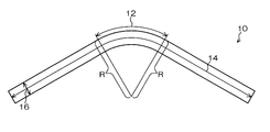
なお、図1に示すように、「折れ曲がっているワイヤー10」とは、ワイヤーの外接12の曲率半径が小さい粒子を言う。具体的には、外接の曲率半径Rが150nmより小さく曲がっているワイヤーが10%以下と少ないことが特徴である。曲率が連続的に変化しながら折れ曲がっている場合には、その曲率半径の最も小さい部分を曲率半径とする。
折れ曲がっているワイヤーは、インクにおける透過型電子顕微鏡(TEM)観察、塗布膜における走査型電子顕微鏡(SEM)観察等の通常の手段で測定することができるが、折れ曲がったワイヤーは塗布までの過程において絡まったりして凝集し易く、固まって存在する場合が多いので、分散した領域のみのTEM、及びSEM写真において粒子を観察するだけでは正確な割合を求めることができない。何枚かのTEM、及びSEM写真を観察し、折れ曲がった粒子がほとんど無かったとしても、まれに存在する粒子の凝集体中には高い割合で折れ曲がり粒子が存在する。よって凝集した領域を含めた全ての粒子について多くの粒子を観察する必要が有る。そのため、10000本以上の粒子について折れ曲がりの有無を観察し、折れ曲がった粒子/全粒子の割合を数えることによって正確な折れ曲がり粒子の割合を求めることができる。
本発明の透明導電性インク及び透明導電性塗布膜は、以下に記載の製造方法により製造される。
<<金属ナノワイヤー分散液>>
前記金属ナノワイヤー分散液は、金属ナノワイヤーを含み、溶媒、分散剤、更に必要に応じてその他の成分を含有してなるものであり、導電性インクとも呼ぶ。
前記金属ナノワイヤー分散液は、金属ナノワイヤーを含み、溶媒、分散剤、更に必要に応じてその他の成分を含有してなるものであり、導電性インクとも呼ぶ。
-金属ナノワイヤー-
本発明において、金属ナノワイヤーとは、短軸径(直径)が50nm以下であり、かつ平均長軸径(長さ)が1μm以上である粒子を示すものとする。
本発明において、金属ナノワイヤーとは、短軸径(直径)が50nm以下であり、かつ平均長軸径(長さ)が1μm以上である粒子を示すものとする。
金属ナノワイヤーが細い金属ナノワイヤーの場合には折れ曲がりが生じやすく、本発明は特に有効である。
前記金属ナノワイヤーの平均短軸径は50nm以下が好ましく、30nm以下がより好ましく、20nm以下がさらに好ましい。なお、前記短軸径は5nm以上とすることで対酸化性を持たせることが出来るため、好ましい。また、前記平均短軸径が50nm以下とすることで、金属ナノワイヤー起因の散乱を抑制し、透明性を高くすることが出来るため、好ましい。
前記金属ナノワイヤーの平均長軸径は、1μm以上が好ましく、5μm以上がより好ましい。なお、金属ナノワイヤーの長軸径は1mm以下とすることで、製造過程で凝集物が生じにくく出来るため、好ましい。また、前記平均長軸径を1μm以上とすることでワイヤー同士がネットワークを形成しやすくなって導電性を高めやすいため好ましい。
ここで、前記金属ナノワイヤーの平均短軸径及び平均長軸径は、例えば、透過型電子顕微鏡(TEM)と光学顕微鏡を用い、TEM像や光学顕微鏡像を観察することにより求めることができ、本発明においては、金属ナノワイヤーの短軸径及び長軸径は、透過型電子顕微鏡(TEM)により300個の金属ナノワイヤーを観察し、その平均値から求めたものである。
本発明においては、短軸径が50nm以下でありかつ長軸径が1μm以上である金属ナノワイヤーが、全金属粒子中に金属量で50質量%以上含まれており、60質量%以上が好ましく、75質量%以上がより好ましい。
前記短軸径が50nm以下であり長軸径が1μm以上である金属ナノワイヤーの割合(以下、「適切ワイヤー化率」と称することもある)を50質量%以上とすることで、電導に寄与する金属の割合を高め、特定の金属粒子に電圧が集中することを抑制できるため耐久性を改善しやすく好ましい。また、金属ナノワイヤーは球形などのプラズモン吸収が強い金属粒子よりも透明度を高めやすく好ましい。
ここで、前記適切ワイヤー化率は、例えば金属ナノワイヤーが銀ナノワイヤーである場合には、銀ナノワイヤー水分散液をろ過して銀ナノワイヤーとそれ以外の粒子を分離し、ICP発光分析装置を用いて、ろ紙に残っている銀(Ag)量と、ろ紙を透過したAg量とを各々測定することで、適切ワイヤー化率を求めることができる。ろ紙に残っている金属ナノワイヤーを透過型電子顕微鏡(TEM)で観察し、300個の金属ナノワイヤーの短軸径を観察し、その分布を調べることにより、短軸径が50nm以下でありかつ長軸径が1μm以上である金属ナノワイヤーであることを確認する。なお、ろ紙は、TEM像で短軸径が50nm以下であり、かつ長軸径が1μm以上である金属ナノワイヤー以外の粒子の最長軸を計測し、その最長軸の5倍以上でありかつワイヤー長軸の最短長の1/2以下の径のものを用いることが好ましい。
本発明の金属ナノワイヤーの短軸径(直径)の変動係数は、40%以下が好ましく、35%以下がより好ましく、30%以下が更に好ましい。
前記変動係数が、40%を超えると、短軸径の短いワイヤーに電圧が集中してしまうためか、耐久性が悪化することがある。
前記金属ナノワイヤーの短軸径の変動係数は、例えば透過型電子顕微鏡(TEM)像から300個のナノワイヤーの短軸径を計測し、その標準偏差と平均値を計算することにより、求めることができる(短軸径の変動係数=短軸径の標準偏差/短軸径の平均値)。
本発明の金属ナノワイヤーの形状としては、例えば円柱状、直方体状、断面が多角形となる柱状など任意の形状をとることができるが、高い透明性が必要とされる用途では、円柱状や断面の多角形の角が丸まっている断面形状であることが好ましい。
前記金属ナノワイヤーの断面形状は、基材上に金属ナノワイヤー水分散液を塗布、乾燥し、膜の断面を透過型電子顕微鏡(TEM)で観察することにより調べることができる。
前記金属ナノワイヤーにおける金属としては、特に制限はなく、いかなる金属であってもよく、1種の金属以外にも2種以上の金属を組み合わせて用いてもよく、合金として用いることも可能である。これらの中でも、金属又は金属化合物から形成されるものが好ましく、金属から形成されるものがより好ましい。
前記金属としては、銅、銀、金、白金、パラジウム、ニッケル、錫、コバルト、ロジウム、イリジウム、鉄、ルテニウム、オスミウム、マンガン、モリブデン、タングステン、ニオブ、タンテル、チタン、ビスマス、アンチモン、鉛、又はこれらの合金などが挙げられる。これらの中でも、銅、銀、金、白金、パラジウム、ニッケル、錫、コバルト、ロジウム、イリジウム又はこれらの合金が好ましく、パラジウム、銅、銀、金、白金、錫及びこれらの合金がより好ましく、銀又は銀を含有する合金が特に好ましい。
前記金属ナノワイヤーの前記金属ナノワイヤー分散液における含有量は、0.1質量%~99質量%が好ましく、0.3質量%~95質量%がより好ましい。
<<金属ナノワイヤーの製造方法>>
前記金属ナノワイヤーの製造方法としては、特に制限はなく、目的に応じて適宜選択することができ、例えば(1)ポリオール法(米国特許出願公開第2005/0056118号明細書、米国特許出願公開第2007/0074316号明細書参照)、(2)少なくともハロゲン化合物、及び還元剤を含む水溶媒中に、金属錯体溶液を添加して加熱する工程と、好ましくは脱塩処理工程とを含む金属ナノワイヤーの製造方法、などが挙げられる。これらの中でも、前記(2)の金属ナノワイヤーの製造方法が特に好ましい。
前記金属ナノワイヤーの製造方法としては、特に制限はなく、目的に応じて適宜選択することができ、例えば(1)ポリオール法(米国特許出願公開第2005/0056118号明細書、米国特許出願公開第2007/0074316号明細書参照)、(2)少なくともハロゲン化合物、及び還元剤を含む水溶媒中に、金属錯体溶液を添加して加熱する工程と、好ましくは脱塩処理工程とを含む金属ナノワイヤーの製造方法、などが挙げられる。これらの中でも、前記(2)の金属ナノワイヤーの製造方法が特に好ましい。
<<前記(2)の金属ナノワイヤーの製造方法>>
前記(2)の金属ナノワイヤーの製造方法は、少なくともハロゲン化合物、及び還元剤を含む水溶媒中に、金属錯体溶液を添加して加熱する工程と、好ましくは脱塩処理工程とを含み、更に必要に応じてその他の工程を含んでなる。
前記(2)の金属ナノワイヤーの製造方法は、少なくともハロゲン化合物、及び還元剤を含む水溶媒中に、金属錯体溶液を添加して加熱する工程と、好ましくは脱塩処理工程とを含み、更に必要に応じてその他の工程を含んでなる。
-金属錯体-
前記金属錯体としては、特に制限はなく、目的に応じて適宜選択することができるが、銀錯体が特に好ましい。前記銀錯体の配位子としては、例えばNO3-、CN-、SCN-、SO3 2-、チオウレア、アンモニアなどが挙げられる。これらについては、“The Theory of the Photographic Process 4th Edition”Macmillan Publishing、T.H.James著の記載を参照することができる。これらの中でも、硝酸銀、銀アンモニア錯体が特に好ましい。
前記金属錯体としては、特に制限はなく、目的に応じて適宜選択することができるが、銀錯体が特に好ましい。前記銀錯体の配位子としては、例えばNO3-、CN-、SCN-、SO3 2-、チオウレア、アンモニアなどが挙げられる。これらについては、“The Theory of the Photographic Process 4th Edition”Macmillan Publishing、T.H.James著の記載を参照することができる。これらの中でも、硝酸銀、銀アンモニア錯体が特に好ましい。
前記金属錯体の添加は、分散剤とハロゲン化合物の後に添加することが好ましい。ワイヤー核を高い確率で形成できるためか、本発明における適切な短軸径や長軸径の金属ナノワイヤーの割合を高める効果がある。
前記溶媒としては、親水性溶媒が好ましく、該親水性溶媒としては、例えば水、メタノール、エタノール、プロパノール、イソプロパノール、ブタノール等のアルコール類;ジオキサン、テトラヒドロフラン等のエーテル類;アセトン等のケトン類;テトラヒドロフラン、ジオキサン等の環状エーテル類、などが挙げられる。
加熱温度は、150℃以下が好ましく、20℃以上130℃以下がより好ましく、30℃以上100℃以下が更に好ましく、40℃以上90℃以下が特に好ましい。必要であれば、粒子形成過程で温度を変更してもよく、途中での温度変更は核形成の制御や再核発生の抑制、選択成長の促進による単分散性向上の効果があることがある。
前記加熱温度が、150℃以下とすることで、ナノワイヤーの断面の角を丸く出来、塗布膜評価での透過率を高めやすくなるため好ましい。また、前記加熱温度を20℃以上とすることで、ワイヤーの長さを適切な範囲に調節でき分散安定性を良く出来るため好ましい。
-還元剤-
前記加熱の際には還元剤を添加して行うことが好ましい。該還元剤としては、特に制限はなく、通常使用されるものの中から適宜選択することができ、例えば、水素化ホウ素ナトリウム、水素化ホウ素カリウム等の水素化ホウ素金属塩;水素化アルミニウムリチウム、水素化アルミニウムカリウム、水素化アルミニウムセシウム、水素化アルミニウムベリリウム、水素化アルミニウムマグネシウム、水素化アルミニウムカルシウム等の水素化アルミニウム塩;亜硫酸ナトリウム、ヒドラジン化合物、デキストリン、ハイドロキノン、ヒドロキシルアミン、クエン酸又はその塩、コハク酸又はその塩、アスコルビン酸又はその塩等;ジエチルアミノエタノール、エタノールアミン、プロパノールアミン、トリエタノールアミン、ジメチルアミノプロパノール等のアルカノールアミン;プロピルアミン、ブチルアミン、ジプロピレンアミン、エチレンジアミン、トリエチレンペンタミン等の脂肪族アミン;ピペリジン、ピロリジン、Nメチルピロリジン、モルホリン等のヘテロ環式アミン;アニリン、N-メチルアニリン、トルイジン、アニシジン、フェネチジン等の芳香族アミン;ベンジルアミン、キシレンジアミン、N-メチルベンジルアミン等のアラルキルアミン;メタノール、エタノール、2-プロパノール等のアルコール;エチレングリコール、グルタチオン、有機酸類(クエン酸、リンゴ酸、酒石酸等)、還元糖類(グルコース、ガラクトース、マンノース、フルクトース、スクロース、マルトース、ラフィノース、スタキオース等)、糖アルコール類(ソルビトール等)などが挙げられる。これらの中でも、還元糖類、還元糖類の誘導体としての糖アルコール類が特に好ましい。なお、還元剤種によっては機能として分散剤としても働く場合があり、同様に好ましく用いることができる。
前記加熱の際には還元剤を添加して行うことが好ましい。該還元剤としては、特に制限はなく、通常使用されるものの中から適宜選択することができ、例えば、水素化ホウ素ナトリウム、水素化ホウ素カリウム等の水素化ホウ素金属塩;水素化アルミニウムリチウム、水素化アルミニウムカリウム、水素化アルミニウムセシウム、水素化アルミニウムベリリウム、水素化アルミニウムマグネシウム、水素化アルミニウムカルシウム等の水素化アルミニウム塩;亜硫酸ナトリウム、ヒドラジン化合物、デキストリン、ハイドロキノン、ヒドロキシルアミン、クエン酸又はその塩、コハク酸又はその塩、アスコルビン酸又はその塩等;ジエチルアミノエタノール、エタノールアミン、プロパノールアミン、トリエタノールアミン、ジメチルアミノプロパノール等のアルカノールアミン;プロピルアミン、ブチルアミン、ジプロピレンアミン、エチレンジアミン、トリエチレンペンタミン等の脂肪族アミン;ピペリジン、ピロリジン、Nメチルピロリジン、モルホリン等のヘテロ環式アミン;アニリン、N-メチルアニリン、トルイジン、アニシジン、フェネチジン等の芳香族アミン;ベンジルアミン、キシレンジアミン、N-メチルベンジルアミン等のアラルキルアミン;メタノール、エタノール、2-プロパノール等のアルコール;エチレングリコール、グルタチオン、有機酸類(クエン酸、リンゴ酸、酒石酸等)、還元糖類(グルコース、ガラクトース、マンノース、フルクトース、スクロース、マルトース、ラフィノース、スタキオース等)、糖アルコール類(ソルビトール等)などが挙げられる。これらの中でも、還元糖類、還元糖類の誘導体としての糖アルコール類が特に好ましい。なお、還元剤種によっては機能として分散剤としても働く場合があり、同様に好ましく用いることができる。
前記還元剤の添加のタイミングは、分散剤の添加前でも添加後でもよく、ハロゲン化合物の添加前でも添加後でもよい。
-ハロゲン化合物-
本発明の金属ナノワイヤー製造の際にはハロゲン化合物を添加して行うことが好ましい。
本発明の金属ナノワイヤー製造の際にはハロゲン化合物を添加して行うことが好ましい。
前記ハロゲン化合物としては、臭素、塩素、ヨウ素を含有する化合物であれば特に制限はなく、目的に応じて適宜選択することができ、例えば、臭化ナトリウム、塩化ナトリウム、ヨウ化ナトリウム、臭化カリウム、塩化カリウム、ヨウ化カリウムなどのアルカリハライドや下記の分散剤と兼用できる物質が好ましい。ハロゲン化合物の添加タイミングは、分散剤の添加前でも添加後でもよく、還元剤の添加前でも添加後でもよい。
なお、ハロゲン化合物種によっては、分散剤として機能するものがありうるが、同様に好ましく用いることができる。
前記ハロゲン化合物の代替としてハロゲン化金属微粒子を使用してもよいし、ハロゲン化合物とハロゲン化金属微粒子を共に使用してもよい。
ハロゲン化合物、又はハロゲン化金属微粒子は分散剤として機能するものもあり好ましく使用される。分散剤の機能を有するハロゲン化合物としては、例えば、アミノ基と臭化物イオンを含むヘキサデシルトリメチルアンモニウムブロミド(HTAB)アミノ基と塩化物イオンを含むヘキサデシルトリメチルアンモニウムクロリド(HTAC)などが挙げられる。
-分散剤-
前記金属ナノワイヤー製造の際には分散剤を添加して行うことが好ましい。なお、使用する分散剤の種類によって得られる金属ナノワイヤーの形状を変化させることができる。前記分散剤を添加する段階は、粒子調製する前に添加し、分散ポリマー存在下で添加してもよいし、粒子調整後に分散状態の制御のために添加しても構わない。分散剤の添加を二段階以上に分けるときには、その量は必要とするワイヤーの長さにより変更する必要がある。これは核となる金属粒子量の制御によるワイヤーの長さに起因しているためと考えられる。
前記金属ナノワイヤー製造の際には分散剤を添加して行うことが好ましい。なお、使用する分散剤の種類によって得られる金属ナノワイヤーの形状を変化させることができる。前記分散剤を添加する段階は、粒子調製する前に添加し、分散ポリマー存在下で添加してもよいし、粒子調整後に分散状態の制御のために添加しても構わない。分散剤の添加を二段階以上に分けるときには、その量は必要とするワイヤーの長さにより変更する必要がある。これは核となる金属粒子量の制御によるワイヤーの長さに起因しているためと考えられる。
前記分散剤としては、特に制限はなく、目的に応じて適宜選択することができ、例えば第4級アルキルアンモニウム塩等のイオン性界面活性剤;アミノ基含有化合物、チオール基含有化合物、スルフィド基含有化合物、アミノ酸又はその誘導体、ペプチド化合物、多糖類、多糖類由来の天然高分子、合成高分子、又はこれらに由来するゲル等の高分子類、などが挙げられる。これらの中でも、浸漬時に洗浄することが容易であるため第4級アルキルアンモニウム塩が特に好ましい。
前記第4級アルキルアンモニウム塩としては、例えばヘキサデシルトリメチルアンモニウムブロミド(HTAB)、ヘキサデシルトリメチルアンモニウムクロリド、ステアリルトリメチルアンモニウムブロミド(STAB)、ステアリルトリメチルアンモニウムクロリド、テトラデシルトリメチルアンモニウムブロミド、テトラデシルトリメチルアンモニウムクロリド、ジラウリルジメチルアンモニウムブロミド、ジラウリルジメチルアンモニウムクロリドなどが挙げられる。これらは、1種単独で使用してもよいし、2種以上を併用してもよい。これらの中でも、ヘキサデシルトリメチルアンモニウムブロミド(HTAB)が特に好ましい。
前記高分子類としては、例えば保護コロイド性のあるポリマーでゼラチン、ポリビニルアルコール、メチルセルロース、ヒドロキシプルピルセルロース、ポリアルキレンアミン、ポリアクリル酸の部分アルキルエステル、ポリビニルピロリドン(PVP)、ポリビニルピロリドン共重合体、などが挙げられる。
前記分散剤として使用可能な構造については、例えば「顔料の事典」(伊藤征司郎編、株式会社朝書院発行、2000年)の記載を参照できる。
-分散溶媒-
前記金属ナノワイヤー分散液における分散溶媒としては、主として水が用いられ、水と混和する有機溶媒を80容量%以下の割合で併用することができる。
前記金属ナノワイヤー分散液における分散溶媒としては、主として水が用いられ、水と混和する有機溶媒を80容量%以下の割合で併用することができる。
前記有機溶媒としては、例えば、沸点が50℃~250℃、より好ましくは55℃~200℃のアルコール系化合物が好適に用いられる。このようなアルコール系化合物を併用することにより、塗布工程での塗り付け良化、乾燥負荷の低減をすることができる。
前記アルコール系化合物としては、特に制限はなく、目的に応じて適宜選択することができ、例えばメタノール、エタノール、エチレングリコール、ジエチレングリコール、トリエチレングリコール、ポリエチレングリコール200、ポリエチレングリコール300、グリセリン、プロピレングリコール、ジプロピレングリコール、1,3-プロパンジオール、1,2-ブタンジオール、1,4-ブタンジオール、1,5-ペンタンジオール、1-エトキシ-2-プロパノール、エタノールアミン、ジエタノールアミン、2-(2-アミノエトキシ)エタノール、2-ジメチルアミノイソプロパノール、などが挙げられる。これらは、1種単独で使用してもよいし、2種以上を併用してもよい。
-脱塩処理-
前記脱塩処理は、金属ナノワイヤーを形成した後、限外ろ過、透析、ゲルろ過、デカンテーション、遠心分離などの手法により行うことができる。
前記脱塩処理は、金属ナノワイヤーを形成した後、限外ろ過、透析、ゲルろ過、デカンテーション、遠心分離などの手法により行うことができる。
この脱塩処理や以下に述べる分散溶媒による分散処理の際に、金属ワイヤーに応力がかかりやすく折れ曲がり易い。
金属ナノワイヤーの成長のメカニズム上、ワイヤー成長におけるワイヤーが折れ曲がって成長するとは考え難く、折れ曲がったワイヤーは、成長の途中もしくは、ワイヤー形成後から透明導電膜を作成する過程でワイヤーに局部的な応力が掛かることによって起こると考えられる。
ワイヤーの折れ曲がりは、ワイヤーの成長工程以降の工程において如何なる段階でも起こりえるが、特にワイヤーの脱塩、分散工程において起こることが多い。これは、各工程、特に脱塩と分散の工程においてワイヤーに応力が掛かっているためと考えられる。
したがって、本発明の少なくとも金属ナノワイヤーを含有する透明導電性インク、及び透明導電性塗布膜は、金属ナノワイヤーのうち折れ曲がっているワイヤーの割合が10%以下であり、好ましくは、折れ曲がっているワイヤーの割合は、2.5%以下であるが、折れ曲がっているワイヤーを少なくするには、脱塩処理と分散処理において、ワイヤーに応力が掛からないようにすることが必要である。
前記金属ナノワイヤー分散液中の、アルカリ金属イオン、アルカリ土類金属イオン、ハロゲン化物イオン等の無機イオンは、前記脱塩処理、及び分散処理により決定されるが、脱塩が不十分であると分散液中に残存した無機イオンが、導電性部材を作成した際の耐久性の悪化要因となることがあるため、無機イオンをなるべく含まないことが好ましい。
前記金属ナノワイヤー分散液の電気伝導度は、前記脱塩処理、分散処理によって決定されるが、脱塩が不十分であると分散液中に残存した塩が、導電性部材を作成した際の耐久性の悪化要因となることがあるため、金属ナノワイヤー分散液の電気伝導度は、1mS/cm以下が好ましく、0.3mS/cm以下がより好ましい。
前記金属ナノワイヤー分散液の20℃における粘度は、0.5mPa・s~100mPa・sが好ましく、1mPa・s~50mPa・sがより好ましい。
-添加剤-
前記金属ナノワイヤー分散液には、必要に応じて、バインダー、各種の添加剤、例えば、界面活性剤、重合性化合物、酸化防止剤、硫化防止剤、腐食防止剤、粘度調整剤、防腐剤などを含有することができる。
前記金属ナノワイヤー分散液には、必要に応じて、バインダー、各種の添加剤、例えば、界面活性剤、重合性化合物、酸化防止剤、硫化防止剤、腐食防止剤、粘度調整剤、防腐剤などを含有することができる。
前記バインダーとしては、特に制限はなく、目的に応じて適宜選択することができ、例えばゾルゲル硬化物、ゼラチン、ゼラチン誘導体、ガゼイン、寒天、でんぷん、ポリビニルアルコール、ポリアクリル酸共重合体、カルボキシメチルセルロース、ヒドロキシエチルセルロース、ポリビニルピロリドン、デキストラン、などが挙げられる。これらは、1種単独で使用してもよいし、2種以上を併用してもよい。
前記バインダーの前記金属ナノワイヤー分散液における含有量は、特に制限はなく、目的に応じて適宜選択することができるが、銀1質量部に対し、0.01質量部~10質量部が好ましく、0.1質量部~5質量部がより好ましい。
前記腐食防止剤としては、特に制限はなく、目的に応じて適宜選択することができ、アゾール類が好適である。前記アゾール類としては、例えばベンゾトリアゾール、トリルトリアゾール、メルカプトベンゾチアゾール、メルカプトベンゾトリアゾール、メルカプトベンゾテトラゾール、(2-ベンゾチアゾリルチオ)酢酸、3-(2-ベンゾチアゾリルチオ)プロピオン酸、及びこれらのアルカリ金属塩、アンモニウム塩、並びにアミン塩から選ばれる少なくとも1種が挙げられる。前記腐食防止剤を含有することで、優れた防錆効果を発揮することができる。
-基材-
前記金属ナノワイヤー分散液を塗布する基材としては、特に制限はなく、目的に応じて適宜選択することができ、例えば、白板ガラス、青板ガラス、シリカコート青板ガラス等の透明ガラス基板;ポリカーボネート樹脂、ポリエーテルスルホン樹脂、ポリエステル樹脂、アクリル樹脂、塩化ビニル樹脂、芳香族ポリアミド樹脂、ポリアミドイミド樹脂、ポリイミド樹脂等の合成樹脂製シート、フィルム又は基板;アルミニウム板、銅板、ニッケル板、ステンレス板等の金属基板;その他セラミック板、光電変換素子を有する半導体基板などを挙げることができる。これらの基板には所望により、シランカップリング剤等の薬品処理、プラズマ処理、イオンプレーティング、スパッタリング、気相反応法、真空蒸着などの前処理を行うことができる。
前記金属ナノワイヤー分散液を塗布する基材としては、特に制限はなく、目的に応じて適宜選択することができ、例えば、白板ガラス、青板ガラス、シリカコート青板ガラス等の透明ガラス基板;ポリカーボネート樹脂、ポリエーテルスルホン樹脂、ポリエステル樹脂、アクリル樹脂、塩化ビニル樹脂、芳香族ポリアミド樹脂、ポリアミドイミド樹脂、ポリイミド樹脂等の合成樹脂製シート、フィルム又は基板;アルミニウム板、銅板、ニッケル板、ステンレス板等の金属基板;その他セラミック板、光電変換素子を有する半導体基板などを挙げることができる。これらの基板には所望により、シランカップリング剤等の薬品処理、プラズマ処理、イオンプレーティング、スパッタリング、気相反応法、真空蒸着などの前処理を行うことができる。
<<金属ナノワイヤー含有膜作製工程>>
金属ナノワイヤー含有膜作製工程は、金属ナノワイヤー及び分散剤を含有する金属ナノワイヤー含有膜を作製する工程である。
金属ナノワイヤー含有膜作製工程は、金属ナノワイヤー及び分散剤を含有する金属ナノワイヤー含有膜を作製する工程である。
この場合、前記金属ナノワイヤー含有膜の作製は、金属ナノワイヤー及び分散剤を含む金属ナノワイヤー分散液を基材上に塗布し、乾燥させて行われることが好ましい。
金属ナノワイヤー分散液を塗布する方法は、例えば、スピンコート法、キャスト法、ロールコート法、フローコート法、プリント法、ディップコート法、流延製膜法、バーコート法、グラビア印刷法、ダイコート法などが挙げられる。
なお、金属ナノワイヤー分散液調製における精製工程は、限外ろ過方式であり、限外ろ過で用いる送液ポンプは、チューブポンプ、モーノポンプ、ダイヤフラムポンプ、ロータリーポンプの何れかであることが好ましい。
限外濾過装置は、少なくとも精製の対象となる金属ナノワイヤー粗分散液が貯蔵されるタンクと、タンク内の金属ナノワイヤー粗分散液を濾液と濃縮液とに分離するフィルタと、タンク内の金属ナノワイヤー粗分散液を送液するためのポンプと、を有している。また、装置内を循環する液の温度制御のために、熱交換器を備えていてもよい。さらに、濾過条件をより正確に把握するために、フィルタの上流側と、フィルタと熱交換器との間にそれぞれ圧力計を備えていてもよい。
前記フィルタの材質としては、使用する物に特に制限はなく、セルロース系、ポリエーテルスルホン酸系、及びPTFE等から選択される高分子部材の中空糸膜を用いることもできるし、多孔質のセラミック膜を用いることもできる。
前記フィルタのポアサイズは、塩を洗浄することができれば特に制限無く自由に選択することができ、金属ナノワイヤー合成時の低分子分散剤も除去することができるサイズであればより好ましく、混合工程で添加した高分子分散剤の余剰分を除去することができるサイズであればより好ましく、金属ナノワイヤー合成工程で生じたワイヤ形状以外の副生成粒子(以下ノイズ粒子と表記する)を除去することのできるサイズであれば更に好ましい。具体的には、ポアサイズは40オングストローム以上が好ましく、100オングストローム以上がより好ましく、500オングストローム以上が更に好ましい。また、ポアサイズが大きすぎると、金属ナノワイヤーがポアに詰まって凝集してしまうことがあるため、ポアサイズは5μm以下が好ましく、1μm以下がより好ましく、0.25μm以下が更に好ましい。
限外濾過による精製工程について説明する。精製対象となる金属ナノワイヤ粗分散液をタンクに投入し、送液ポンプを動作させ、装置内を循環させる。金属ナノワイヤ粗分散液がフィルタを通過する際に、フィルタ外に溶媒の一部が濾液として排出されるため、金属ナノワイヤ粗分散液はフィルタ通過前よりも濃縮されてタンクに戻る。適宜タンク内に未精製の金属ナノワイヤー粗分散液が追加供給されながら、前述した工程を繰り返すことによって、金属ナノワイヤー粗分散液の濃縮が行われる。
金属ナノワイヤ粗分散液の濃縮終了後、タンクに洗浄溶媒を投入し、濃縮された金属ナノワイヤ粗分散液の洗浄を行う。洗浄溶媒を適宜供給しながら、フィルタからの濾液排出を繰り返すことで、金属ナノワイヤーの濃度の変動を抑えた状態で、金属ナノワイヤ粗分散液の洗浄と溶媒の置換を行うことができる。
本態様における精製工程では、必要に応じてフィルタ部に圧力をかけ、濾過速度を調整することができる。このフィルタの上下での圧力の平均を濾過圧と定義する。濾過圧が高すぎると、フィルタに堆積した固形分が圧縮され、後述する逆洗でフィルタ面から固形分を除去しても再分散しないことがあるため、濾過圧は0.5MPa以下が好ましく、0.4MPa以下がより好ましく、0.2MPa以下が更に好ましい。また、濾過圧が低すぎると濾過流量が低くなり、工程時間が長くなるため、0.01MPa以上が好ましく、0.02MPa以上が好ましく、0.03MPa以上が更に好ましい。
本態様における精製工程では、フィルタへの固形分の堆積による濾過効率の低減を抑止するために、濃縮及び洗浄実施中に定期的に逆洗を行うことが望ましい。逆洗とは、濾液と接しているフィルタ面から分散液が接している面へ濾液を押し返す操作である。濾液を押し返すために、例えばエアなどのガスを用いて、濾液流路に濾液排出方向とは逆方向に濾液を加圧してもよい。濾液を押し返す圧力の大きさは、押し返すためにガスを使用する場合、前記濾過圧と濾液を押し返すためのガス圧との差で定義され、これを逆洗圧とする。逆洗圧は、フィルタに堆積した固形分をフィルタ面から除去することができれば特に制限はないが、圧力が低すぎるとフィルタに堆積した固形分を除去することができなくなるため、0.1MPa以上であることが好ましく、0.2MPa以上であることがより好ましく、0.3MPa以上であることが更に好ましい。また、圧力が高すぎると押し返すために使用したガスが分散液内に混入してしまい、循環流路内の流れを乱してしまうことがあるため、10MPa以下が好ましく、5MPa以下であることがより好ましく、3MPa以下であることが更に好ましい。また、逆洗を実施する間隔としては、フィルタ面に堆積した固形分を除去することができれば特に制限はないが、間隔が広すぎるとフィルタ面から固形分を除去することができなくなるため、30分間隔以下が好ましく、15分間隔以下がより好ましく、10分以下が更に好ましい。また、逆洗を実施している間は濾過が実施されないため、逆洗間隔が短すぎると、工程時間が長くなってしまうことから、15秒以上が好ましく、1分以上がより好ましく、3分以上が更に好ましい。
前記精製工程では、金属ナノワイヤー粗分散液を濃縮した後、洗浄液を添加することにより、金属濃度を過度に上昇させることなく分散液の精製を実施することができる。洗浄液としては、金属ナノワイヤが凝集しなければ特に制限無く用いることができる。特に、除去したい塩、金属ナノワイヤー合成時の低分子分散剤、混合工程で添加した余剰の高分子分散剤が溶解する洗浄液であることが好ましい。
以上のようにして作製された透明導電性塗布膜の厚みは、0.02μm~1μmが好ましく、0.03μm~0.3μmがより好ましい。
本発明の導電膜の表面抵抗は、150Ω/□以下が好ましい。
ここで、前記表面抵抗は、例えば四端子法により測定することができる。
本発明の透明導電性塗布膜の光透過率は、92%以上が好ましい。本発明の透明導電性塗布膜のヘイズ値は、1.0%以下が好ましく、0.6%以下であることがより好ましい。
ここで、前記透過率は、例えば紫外可視分光光度計(UV2400-PC、島津製作所製)により測定することができ、前記ヘイズ値は、例えばヘイズガードプラス(ガードナー社製)により測定することができる。
本発明の透明導電性塗布膜は、透明性と導電性を大幅に向上させることができるので、例えばタッチパネル、ディスプレイ用電極、電磁波シールド、有機又は無機ELディスプレイ用電極、電子ペーパー、フレキシブルディスプレイ用電極、集積型太陽電池、表示素子、その他の各種デバイスなどに幅広く適用される。これらの中でも、タッチパネル、表示素子、集積型太陽電池が好ましく、タッチパネルが特に好ましい。
(タッチパネル)
本発明の透明導電性塗布膜をタッチパネルの透明導電体として使用した場合、透過率の向上により視認性に優れ、かつ導電性の向上により素手、手袋を嵌めた手、指示具のうち少なくとも一つによる文字等の入力又は画面操作に対し応答性に優れるタッチパネルを製作することができる。
本発明の透明導電性塗布膜をタッチパネルの透明導電体として使用した場合、透過率の向上により視認性に優れ、かつ導電性の向上により素手、手袋を嵌めた手、指示具のうち少なくとも一つによる文字等の入力又は画面操作に対し応答性に優れるタッチパネルを製作することができる。
前記タッチパネルとしては、広く公知のタッチパネルが挙げられ、いわゆるタッチセンサー及びタッチパッドとして知られているものに対して、本発明の透明導電性塗布膜を適用することができる。
前記タッチパネルとしては、前記透明導電性塗布膜を有する限り特に制限はなく、目的に応じて適宜選択することができ、例えば、表面型静電容量方式タッチパネル、投射型静電容量方式タッチパネル、抵抗膜式タッチパネルなどが挙げられる。
((実施例1))
<<銀ナノワイヤー分散液1>>
〔添加液B〕
硝酸銀 2.6mgをエチレングリコール100mlに溶かした。
<<銀ナノワイヤー分散液1>>
〔添加液B〕
硝酸銀 2.6mgをエチレングリコール100mlに溶かした。
〔添加液C〕
硝酸銀 17gをエチレングリコール1000mlに溶かした。
硝酸銀 17gをエチレングリコール1000mlに溶かした。
〔添加液D〕
PVP 56gをエチレングリコール1000mlに溶かした。
PVP 56gをエチレングリコール1000mlに溶かした。
Adv.Mater. 2002 14 833-837に書かれた方法を参考に以下の方法にて銀ナノワイヤー分散液1を合成した。
170℃で加熱したエチレングリコール溶液1000mlを攪拌しながら添加液B全量を7秒間で添加した。2時間後に攪拌を100rpmにし、添加液C全量と添加液D全量を同時に100分間かけて添加し、銀ナノワイヤー分散液1を得た。
<<銀ナノワイヤー分散液2>>
予め、下記の添加液A、G、及びHを調製した。
予め、下記の添加液A、G、及びHを調製した。
〔添加液A〕
硝酸銀粉末0.90gを純水150mLに溶解した。その後、1Nのアンモニア水を透明になるまで添加した。そして、全量が300mLになるように純水を添加した。
硝酸銀粉末0.90gを純水150mLに溶解した。その後、1Nのアンモニア水を透明になるまで添加した。そして、全量が300mLになるように純水を添加した。
〔添加液G〕
グルコース粉末1.0gを280mLの純水で溶解して、添加液Gを調製した。
グルコース粉末1.0gを280mLの純水で溶解して、添加液Gを調製した。
〔添加液H〕
HTAB(ヘキサデシル-トリメチルアンモニウムブロミド)粉末0.5gを27.5mLの純水で溶解して、添加液Hを調製した。
HTAB(ヘキサデシル-トリメチルアンモニウムブロミド)粉末0.5gを27.5mLの純水で溶解して、添加液Hを調製した。
次に、以下のようにして、銀ナノワイヤー分散液2を調製した。
純水410mLを三口フラスコ内に入れ、20℃にて攪拌しながら、添加液H 82.5mL、及び添加液G 206mLをロートにて添加した(一段目)。この液に、添加液A 206mLを流量2.0mL/min、攪拌回転数800rpmで添加した(二段目)。その10分間後、添加液Hを82.5mL添加した(三段目)。その後、3℃/分で内温85℃まで昇温した。その後、攪拌回転数を1000rpmとし、5時間加熱した。
<<銀ナノワイヤー分散液3>>
添加する添加液Aの硝酸銀濃度を2倍にして添加する以外は銀ナノワイヤー分散液2と同様にして銀ナノワイヤー分散液3を得た。
添加する添加液Aの硝酸銀濃度を2倍にして添加する以外は銀ナノワイヤー分散液2と同様にして銀ナノワイヤー分散液3を得た。
<<銀ナノワイヤー分散液4>>
銀ナノワイヤー分散液3において、85℃に昇温した後の攪拌回転数を1000rpmではなく100rpmに落とした以外は銀ナノワイヤー分散液2と同様にして銀ナノワイヤー分散液4を得た。
銀ナノワイヤー分散液3において、85℃に昇温した後の攪拌回転数を1000rpmではなく100rpmに落とした以外は銀ナノワイヤー分散液2と同様にして銀ナノワイヤー分散液4を得た。
<<銀ナノワイヤー分散液5>>
銀ナノワイヤー分散液2において、内温85℃、攪拌回転数1000rpmでの加熱時間を5時間から2時間に変更した以外は、銀ナノワイヤー分散液2と同様にして、銀ナノワイヤー分散液5を得た。
銀ナノワイヤー分散液2において、内温85℃、攪拌回転数1000rpmでの加熱時間を5時間から2時間に変更した以外は、銀ナノワイヤー分散液2と同様にして、銀ナノワイヤー分散液5を得た。
[銀ナノワイヤーの平均短軸径(平均直径)及び平均長軸径]
透過型電子顕微鏡(TEM;日本電子株式会社製、JEM-2000FX)を用い、300個の銀ナノワイヤーを観察し、銀ナノワイヤーの平均短軸径及び平均長軸径を求めた。
透過型電子顕微鏡(TEM;日本電子株式会社製、JEM-2000FX)を用い、300個の銀ナノワイヤーを観察し、銀ナノワイヤーの平均短軸径及び平均長軸径を求めた。
<<サンプル液1の作成>>
銀ナノワイヤー分散液1を100ml取り、日立製CR21G遠心分離で60000rpm30分の遠心分離を行い、上澄みを80ml捨てた後、STM社の超音波分散機UH-300を用いて超音波分散を5分行って分散した。ここにエタノールを80ml加えるという遠心分離-上澄み除去-溶媒添加の操作を5回繰り返した後、遠心分離、上澄みを出来る限り除去し、超音波分散を行った。ここにエタノールではなくプロピレングリコールモノメチルエーテルを100ml加え10分間超音波分散を行い、サンプル液1を得た。
銀ナノワイヤー分散液1を100ml取り、日立製CR21G遠心分離で60000rpm30分の遠心分離を行い、上澄みを80ml捨てた後、STM社の超音波分散機UH-300を用いて超音波分散を5分行って分散した。ここにエタノールを80ml加えるという遠心分離-上澄み除去-溶媒添加の操作を5回繰り返した後、遠心分離、上澄みを出来る限り除去し、超音波分散を行った。ここにエタノールではなくプロピレングリコールモノメチルエーテルを100ml加え10分間超音波分散を行い、サンプル液1を得た。
<<サンプル液2の作成>>
銀ナノワイヤー分散液1を銀ナノワイヤー分散液2に変更する以外はサンプル液1と同様にしてサンプル液2を作成した。
銀ナノワイヤー分散液1を銀ナノワイヤー分散液2に変更する以外はサンプル液1と同様にしてサンプル液2を作成した。
<<サンプル液3の作成>>
銀ナノワイヤー分散液1を銀ナノワイヤー分散液3に変更する以外はサンプル液1と同様にしてサンプル液3を作成した。
銀ナノワイヤー分散液1を銀ナノワイヤー分散液3に変更する以外はサンプル液1と同様にしてサンプル液3を作成した。
<<サンプル液4の作成>>
銀ナノワイヤー分散液3を100mlにソルスパース2400SC(ゼネカ(株)製)の1%トルエン液40mlを加えて攪拌した。更にエタノール200mlを添加し10分間攪拌を続けた。攪拌後に16時間静置し、銀ナノワイヤーが抽出されたトルエン層のみを回収した。このトルエン溶液に更にエタノールを100ml添加し、6000rpm30分の遠心分離を行った。上澄みを出来る限り捨てた後にプロピレングリコールモノメチルエーテルアセテートを100ml加え10分間超音波分散を行い、サンプル液4を得た。
銀ナノワイヤー分散液3を100mlにソルスパース2400SC(ゼネカ(株)製)の1%トルエン液40mlを加えて攪拌した。更にエタノール200mlを添加し10分間攪拌を続けた。攪拌後に16時間静置し、銀ナノワイヤーが抽出されたトルエン層のみを回収した。このトルエン溶液に更にエタノールを100ml添加し、6000rpm30分の遠心分離を行った。上澄みを出来る限り捨てた後にプロピレングリコールモノメチルエーテルアセテートを100ml加え10分間超音波分散を行い、サンプル液4を得た。
<<サンプル液5の作成>>
銀ナノワイヤー分散液2を1000ml取り、0.02mol/lのポリビニルピロリドン(K-30、和光純薬工業株式会社製)の水溶液を500ml添加し、よく攪拌しながら等容量のエタノールを添加した。ろ過孔径0.2μm精密濾過膜UNA620(旭化成株式会社製)、送液ポンプとしてイワキ製MDGR15型ギヤポンプを用いて限外ろ過を行った。モジュールからの濾液が800mlになった時点で濃縮液にエタノール溶液を800mL加える洗浄を連続して2回行った後、濃縮液が200mlになったらプロピレングリコールモノメチルエーテルを800mL加える洗浄を4回行った。その後100mlまで濃縮を行いサンプル液5を得た。
銀ナノワイヤー分散液2を1000ml取り、0.02mol/lのポリビニルピロリドン(K-30、和光純薬工業株式会社製)の水溶液を500ml添加し、よく攪拌しながら等容量のエタノールを添加した。ろ過孔径0.2μm精密濾過膜UNA620(旭化成株式会社製)、送液ポンプとしてイワキ製MDGR15型ギヤポンプを用いて限外ろ過を行った。モジュールからの濾液が800mlになった時点で濃縮液にエタノール溶液を800mL加える洗浄を連続して2回行った後、濃縮液が200mlになったらプロピレングリコールモノメチルエーテルを800mL加える洗浄を4回行った。その後100mlまで濃縮を行いサンプル液5を得た。
<<サンプル液6の作成>>
エタノール溶液を800ml加える洗浄を2回行った後、プロピレングリコールモノメチルエーテルによる洗浄を行なわず、100mlまで濃縮を行う以外は、サンプル液5と同様にして、サンプル液6を得た。
エタノール溶液を800ml加える洗浄を2回行った後、プロピレングリコールモノメチルエーテルによる洗浄を行なわず、100mlまで濃縮を行う以外は、サンプル液5と同様にして、サンプル液6を得た。
<<サンプル液7の作成>>
エタノールによる洗浄、プロピレングリコールモノメチルエーテルによる洗浄、及び濃縮を行わない銀ナノワイヤー分散液2そのものを、サンプル液7とした。
エタノールによる洗浄、プロピレングリコールモノメチルエーテルによる洗浄、及び濃縮を行わない銀ナノワイヤー分散液2そのものを、サンプル液7とした。
<<サンプル液8の作成>>
限外ろ過時の送液ポンプを帝国電気製キャンドポンプ(F60-3211N2BL)に変更する以外は、サンプル液5と同様にして、サンプル液8を得た。
限外ろ過時の送液ポンプを帝国電気製キャンドポンプ(F60-3211N2BL)に変更する以外は、サンプル液5と同様にして、サンプル液8を得た。
<<サンプル液9の作成>>
限外ろ過時の送液ポンプを日機装製3連式プランジャーポンプに変更する以外は、サンプル液5と同様にして、サンプル液9を得た。
限外ろ過時の送液ポンプを日機装製3連式プランジャーポンプに変更する以外は、サンプル液5と同様にして、サンプル液9を得た。
<<サンプル液10の作成>>
限外ろ過時の送液ポンプを、イワキ製WM720型チュービングポンプに変更する以外は、サンプル液5と同様にして、サンプル液10を得た。
限外ろ過時の送液ポンプを、イワキ製WM720型チュービングポンプに変更する以外は、サンプル液5と同様にして、サンプル液10を得た。
<<サンプル液11の作成>>
プロピレングリコールモノメチルエーテルを800mL加える洗浄を4回ではなく2回に変更する以外は、サンプル液10と同様にして、サンプル液11を得た。
プロピレングリコールモノメチルエーテルを800mL加える洗浄を4回ではなく2回に変更する以外は、サンプル液10と同様にして、サンプル液11を得た。
<<サンプル液12の作成>>
銀ナノワイヤー分散液2を銀ナノワイヤー分散液5に変更する以外はサンプル液10と同様にしてサンプル液12を作成した。
銀ナノワイヤー分散液2を銀ナノワイヤー分散液5に変更する以外はサンプル液10と同様にしてサンプル液12を作成した。
<<サンプル液13の作成>>
銀ナノワイヤー分散液2を銀ナノワイヤー分散液3に変更する以外はサンプル液10と同様にしてサンプル液13を作成した。
銀ナノワイヤー分散液2を銀ナノワイヤー分散液3に変更する以外はサンプル液10と同様にしてサンプル液13を作成した。
<<サンプル液14の作成>>
銀ナノワイヤー分散液2を銀ナノワイヤー分散液4に変更する以外はサンプル液10と同様にしてサンプル液14を作成した。
銀ナノワイヤー分散液2を銀ナノワイヤー分散液4に変更する以外はサンプル液10と同様にしてサンプル液14を作成した。
<<サンプル液15の作成>>
限外ろ過時の送液ポンプを兵神装備製モーノポンプ(NL20)に変更する以外は、サンプル液13と同様にして、サンプル液15を得た。
限外ろ過時の送液ポンプを兵神装備製モーノポンプ(NL20)に変更する以外は、サンプル液13と同様にして、サンプル液15を得た。
<<サンプル液16の作成>>
限外ろ過時の送液ポンプをタクミナ製ダイヤフラムポンプ(TPL1MC-014-6T6-CW-4-S)に変更する以外は、サンプル液13と同様にして、サンプル液16を得た。
限外ろ過時の送液ポンプをタクミナ製ダイヤフラムポンプ(TPL1MC-014-6T6-CW-4-S)に変更する以外は、サンプル液13と同様にして、サンプル液16を得た。
<<サンプル液17の作成>>
限外ろ過時の送液ポンプを大同メタル製ロータリーポンプ(RPDTR210COMT212243)に変更する以外は、サンプル液13と同様にして、サンプル液17を得た。
限外ろ過時の送液ポンプを大同メタル製ロータリーポンプ(RPDTR210COMT212243)に変更する以外は、サンプル液13と同様にして、サンプル液17を得た。
<<サンプル液18の作成>>
銀ナノワイヤー分散液3を1000ml取り、0.02mol/lのポリビニルピロリドン(K-30、和光純薬工業株式会社製)の水溶液を500ml添加し、よく攪拌しながら等容量のエタノールを添加した。ろ過孔径0.2μm精密濾過膜UNA620(旭化成株式会社製)、送液ポンプとしてイワキ製WM720型チュービングポンプを用いて限外ろ過を行った。モジュールからの濾液が800mLになった時点で濃縮液にエタノール溶液を800ml加える洗浄を連続して2回行った後、濃縮液が200mlになったら水/1-プロパノール=1/1(質量)溶液を800mL加える洗浄を4回行った後そのまま100mlまで濃縮を行い、サンプル液18を得た。
銀ナノワイヤー分散液3を1000ml取り、0.02mol/lのポリビニルピロリドン(K-30、和光純薬工業株式会社製)の水溶液を500ml添加し、よく攪拌しながら等容量のエタノールを添加した。ろ過孔径0.2μm精密濾過膜UNA620(旭化成株式会社製)、送液ポンプとしてイワキ製WM720型チュービングポンプを用いて限外ろ過を行った。モジュールからの濾液が800mLになった時点で濃縮液にエタノール溶液を800ml加える洗浄を連続して2回行った後、濃縮液が200mlになったら水/1-プロパノール=1/1(質量)溶液を800mL加える洗浄を4回行った後そのまま100mlまで濃縮を行い、サンプル液18を得た。
<<透明導電性塗布膜の作成>>
上記サンプル液1~5、8~18をPET基材上に表面抵抗がほぼ同じになるようにバーの番手を調整してバーコート塗布した。サンプル液6、7については、ヘイズ値が3.0%を超えるまで塗布量を増やしたが、表面抵抗を150Ω/□以下に調整することはできなかった。
上記サンプル液1~5、8~18をPET基材上に表面抵抗がほぼ同じになるようにバーの番手を調整してバーコート塗布した。サンプル液6、7については、ヘイズ値が3.0%を超えるまで塗布量を増やしたが、表面抵抗を150Ω/□以下に調整することはできなかった。
透明導電性インク、及び塗布膜において、折れ曲がっているワイヤーの割合、導電率、透過率、ヘイズ値を測定した。測定方法は以下の通りである。
<折れ曲がっているワイヤーの割合>
インクについては、メッシュに滴下したインクをTEM(日本電子株式会社製、JEM-2000FX)で観察し、10000本のワイヤーについて折れ曲がっているワイヤーの割合を数えた。
インクについては、メッシュに滴下したインクをTEM(日本電子株式会社製、JEM-2000FX)で観察し、10000本のワイヤーについて折れ曲がっているワイヤーの割合を数えた。
塗布膜については、塗布膜をSEM(日立製作所製、S-5200)で観察し、10000本のワイヤーについて折れ曲がっているワイヤーの割合を数えた。
折れ曲がっているワイヤーの割合は、インクと塗布膜でほぼ同じであった。
<ヘイズ・光透過率の測定>
形成後の導電層(又は被転写体に転写した導電層)を、ガードナー社製ヘイズガードプラスを用いて、C光源下のCIE視感度関数yについて、測定角0°で測定した。
形成後の導電層(又は被転写体に転写した導電層)を、ガードナー社製ヘイズガードプラスを用いて、C光源下のCIE視感度関数yについて、測定角0°で測定した。
<表面抵抗の測定>
形成後の導電層(又は被転写体に転写した導電層)を、表面抵抗計(三菱化学株式会社製、Loresta-GP MCP-T600)を用いて、表面抵抗を測定した。
形成後の導電層(又は被転写体に転写した導電層)を、表面抵抗計(三菱化学株式会社製、Loresta-GP MCP-T600)を用いて、表面抵抗を測定した。
パターニングサンプルの抵抗値は、実際の微細パターンの導電部を測定するのは難しいため、実パターンと同サンプル中に評価用パターン(100mm□)を入れておき、導電部の抵抗を測定した。これを5箇所で実施し、平均値を求めた。
<湿熱耐久性>
パターン化導電性部材を、85℃/85%RH(相対湿度)の環境下に120時間暴露し、暴露前の抵抗値をR0、暴露後の抵抗値をRとして、下記のランク付けを行った。なお、ランクの数字は大きいほど性能が良いことを示しており、ランク3以上では実用上問題の無いレベルである。
パターン化導電性部材を、85℃/85%RH(相対湿度)の環境下に120時間暴露し、暴露前の抵抗値をR0、暴露後の抵抗値をRとして、下記のランク付けを行った。なお、ランクの数字は大きいほど性能が良いことを示しており、ランク3以上では実用上問題の無いレベルである。
〔評価基準〕
5: R/R0が1.1以下、0.9以上
4: R/R0が1.2以下、0.8以上
3: R/R0が1.3以下、0.7以上
2: R/R0が1.5以下、0.7以上
1: R/R0が1.5以上、または0.7以下
得られた結果を図2の表に示す。
5: R/R0が1.1以下、0.9以上
4: R/R0が1.2以下、0.8以上
3: R/R0が1.3以下、0.7以上
2: R/R0が1.5以下、0.7以上
1: R/R0が1.5以上、または0.7以下
得られた結果を図2の表に示す。
図2の表の結果から分かるように、少なくとも金属ナノワイヤーを含有する透明導電性塗布膜において、前記金属ナノワイヤーのうち折れ曲がっているワイヤーの割合が10%以下であることで、高い導電性を維持しつつ透過率を高くしヘイズ値を下げることができることが分かる。そして、金属ナノワイヤーのうち折れ曲がっているワイヤーの割合が10%以下であり、且つ導電性インク中の伝道度が、1mS/cm以下であることで、表面抵抗が150Ω/□以下、ヘイズが1.0%以下、透過率が92%以上である透明導電性塗布膜を得ることができることが分かる。
((実施例2))
<<導電層転写材料>>
<<クッション層の作製>>
基材としての平均厚み30μmのポリエチレンテレフタレート(PET)フィルム上に、下記組成のクッション層用塗布液を塗布し、乾燥させて、平均厚み10μmのクッション層を形成した。
<<導電層転写材料>>
<<クッション層の作製>>
基材としての平均厚み30μmのポリエチレンテレフタレート(PET)フィルム上に、下記組成のクッション層用塗布液を塗布し、乾燥させて、平均厚み10μmのクッション層を形成した。
-クッション層用塗布液の組成-
・メチルメタクリレート/2-エチルヘキシルアクリレート/ベンジルメタクリレート/メタクリル酸共重合体(共重合組成比(モル比)=55/30/10/5、重量平均分子量=10万、ガラス転移温度(Tg)=70℃)・・・6.0質量部
・スチレン/アクリル酸共重合体(共重合組成比(モル比)=65/35、重量平均分子量=1万、ガラス転移温度(Tg)=100℃)・・・14.0質量部
・BPE-500(新中村化学株式会社製)・・・9.0質量部
・メガファックF-780-F(大日本インキ化学工業株式会社製)・・0.5質量部
・メタノール・・・10.0質量部
・プロピレングリコールモノメチルエーテルアセテート・・・5.0質量部
・メチルエチルケトン・・・55.5質量部
<<導電層の作製>>
-バインダー(A-1)の合成-
共重合体を構成するモノマー成分として、7.79gのメタクリル酸および37.21gのベンジルメタクリレートを使用し、ラジカル重合開始剤として0.5gのアゾビスイソブチロニトリルを使用し、これらを55.00gのプロピレングリコールモノメチルエーテルアセテート(PGMEA)中において重合反応させることにより下記構造を有するバインダー(A-1)のPGMEA溶液(固形分濃度:40質量%)を得た。なお、重合温度は、温度60℃乃至100℃に調整した。
分子量はゲルパーミエーションクロマトグラフィ(GPC)を用いて測定した結果、ポリスチレン換算による重量平均分子量(Mw)は30,000、分子量分布(Mw/Mn)は2.21であった。

-ネガ型導電層用組成物の調製-
上記バインダー(A-1)0.241質量部、KAYARAD DPHA(日本化薬株式会社製)0.252質量部、IRGACURE379(チバ・スペシャルティ・ケミカルズ株式会社製)0.0252質量部、架橋剤としてのEHPE-3150(ダイセル化学株式会社製)0.0237質量部、メガファックF781F(DIC株式会社製)0.0003質量部、プロピレングリコールモノメチルエーテルアセテート(PGMEA)0.9611質量部、及び1-メトキシ-2-プロパノール(MFG)44.3質量部、前記銀ナノワイヤーのプロピレングリコールモノメチルエーテルアセテート分散液(サンプル液1~17)を加え、攪拌し、ネガ型導電層用組成物を調製した。
上記バインダー(A-1)0.241質量部、KAYARAD DPHA(日本化薬株式会社製)0.252質量部、IRGACURE379(チバ・スペシャルティ・ケミカルズ株式会社製)0.0252質量部、架橋剤としてのEHPE-3150(ダイセル化学株式会社製)0.0237質量部、メガファックF781F(DIC株式会社製)0.0003質量部、プロピレングリコールモノメチルエーテルアセテート(PGMEA)0.9611質量部、及び1-メトキシ-2-プロパノール(MFG)44.3質量部、前記銀ナノワイヤーのプロピレングリコールモノメチルエーテルアセテート分散液(サンプル液1~17)を加え、攪拌し、ネガ型導電層用組成物を調製した。
-導電層の形成-
得られたネガ型導電層用組成物を、表面抵抗がほぼ同じになるように、前記クッション層を形成したフィルム上に塗布し、乾燥させて、平均厚み0.1μmの導電層を形成した。以上により、導電層転写材料を作製した。
得られたネガ型導電層用組成物を、表面抵抗がほぼ同じになるように、前記クッション層を形成したフィルム上に塗布し、乾燥させて、平均厚み0.1μmの導電層を形成した。以上により、導電層転写材料を作製した。
ここで、導電層における金属ナノワイヤー以外の成分の含有量Aと、金属ナノワイヤーの含有量Bとの質量比(A/B)が0.6であった。
<パターニング処理>
被転写体(厚み0.7mmのガラス基板)に、各導電層転写材料の導電層及びクッション層を転写した後、以下の方法により、ラインアンドスペース(以下、L/Sという)=100μm/100μmのストライプ状パターンを作製した。なお、クッション層は、シャワー現像により除去される。
被転写体(厚み0.7mmのガラス基板)に、各導電層転写材料の導電層及びクッション層を転写した後、以下の方法により、ラインアンドスペース(以下、L/Sという)=100μm/100μmのストライプ状パターンを作製した。なお、クッション層は、シャワー現像により除去される。
〔パターニング条件〕
マスク上から、高圧水銀灯i線(365nm)を100mJ/cm2(照度20mW/cm2)露光を行った。露光後の基板を、純水5,000gに炭酸水素ナトリウム5gと炭酸ナトリウム2.5gを溶解した現像液でシャワー現像30秒間を行った。シャワー圧は0.04MPa、ストライプパターンが出現するまでの時間は15秒間であった。次に、純水のシャワーでリンスした。
マスク上から、高圧水銀灯i線(365nm)を100mJ/cm2(照度20mW/cm2)露光を行った。露光後の基板を、純水5,000gに炭酸水素ナトリウム5gと炭酸ナトリウム2.5gを溶解した現像液でシャワー現像30秒間を行った。シャワー圧は0.04MPa、ストライプパターンが出現するまでの時間は15秒間であった。次に、純水のシャワーでリンスした。
実施例1のサンプル液を上記導電層に入れた場合にも同様に本発明の折れ曲がりの少ないナノワイヤーは透過率が高く低ヘイズな効果が得られた。
((実施例3))
<ゾルゲルマトリックス導電層材料>
<<PET基板の作製>>
基材としての平均厚み125μmのポリエチレンテレフタレート(PET)フィルム表面を1J/m2のコロナ放電処理を施した後、下記組成の接着用溶液1を塗布し120℃で2分乾燥させ、厚さが0.11μmの接着層1を形成した。次に、前述の第一の接着層を付与したPET基板に、1J/m2のコロナ放電処理を施した。その後このPET基板に下記組成の接着用溶液2を塗布し170℃で1分間乾燥させ、厚さが0.5μmの接着層2を形成した。次に、前述の第一及び第二の接着層を付与したPET基板に、下記組成の接着用溶液3を塗布し、120℃で1分間乾燥させて、平均厚み1nmの接着層3を形成した。
下記の配合で接着用溶液1、2および3を調製した。
-接着用溶液1-
・タケラックWS-4000 5.0部
(コーティング用ポリウレタン、固形分濃度30%、三井化学(株)製)
・界面活性剤 0.3部
(ナローアクティHN-100、三洋化成工業(株)製)
・界面活性剤 0.3部
(サンデットBL、固形分濃度43%、三洋化成工業(株)製)
・水 94.4部
-接着用溶液2-
・テトラエトキシシラン 5.0部
(KBE-04、信越化学工業(株)製)
・3-グリシドキシプロピルトリメトキシシラン 3.2部
(KBM-403、信越化学工業(株)製)
・2-(3,4-エポキシシクロヘキシル)エチルトリメトキシシラン 1.8部
(KBM-303、信越化学工業(株)製)
・酢酸水溶液(酢酸濃度=0.05%、pH=5.2) 10.0部
・硬化剤 0.8部
(ホウ酸、和光純薬工業(株)製)
・コロイダルシリカ 60.0部
(スノーテックスO、平均粒子径10nmから20nm、固形分濃度20%、pH=2.6、日産化学工業(株)製)
・界面活性剤 0.2部
(ナローアクティHN-100、三洋化成工業(株)製)
・界面活性剤 0.2部
(サンデットBL、固形分濃度43%、三洋化成工業(株)製)
上記接着用溶液2は、以下のようにして調製した。
酢酸水溶液を激しく攪拌しながら、3-グリシドキシプロピルトリメトキシシランを、この酢酸水溶液中に3分間かけて滴下した。次に、2-(3,4-エポキシシクロヘキシル)エチルトリメトキシシランを酢酸水溶液中に強く攪拌しながら3分間かけて添加した。次に、テトラメトキシシランを、酢酸水溶液中に強く攪拌しながら5分かけて添加し、その後2時間攪拌を続けた。次に、コロイダルシリカと、硬化剤と、界面活性剤とを順次添加し、接着用塗布液2とした。
-接着用溶液3-
・N-(2-アミノエチル)-3-アミノプロピルトリメトキシシラン 0.02部
・蒸留水 99.8部
接着用溶液3は、以下の方法で調製した。N-(2-アミノエチル)-3-アミノプロピルトリメトキシシランに水を加え、1時間攪拌し、接着用溶液3とした。
・N-(2-アミノエチル)-3-アミノプロピルトリメトキシシラン 0.02部
・蒸留水 99.8部
接着用溶液3は、以下の方法で調製した。N-(2-アミノエチル)-3-アミノプロピルトリメトキシシランに水を加え、1時間攪拌し、接着用溶液3とした。
<<導電性層の作製>>
前記接着層3まで形成した基材表面を1J/m2のコロナ放電処理を施した後、下記組成の導電性層塗布液を前記基板に塗布し、120℃で1分乾燥させ、厚さが0.04μmの導電性層を形成し、実施例3の導電性部材を得た。
前記接着層3まで形成した基材表面を1J/m2のコロナ放電処理を施した後、下記組成の導電性層塗布液を前記基板に塗布し、120℃で1分乾燥させ、厚さが0.04μmの導電性層を形成し、実施例3の導電性部材を得た。
-導電性層塗布液の調製-
下記組成のアルコキシド化合物の溶液を60℃で1時間撹拌して均一になったことを確
認した。得られたゾルゲル溶液3.44部と前記実施例1で得られた「サンプル液18」16.56部を混合し、さらに蒸留水で希釈して導電性層形成用塗布液を得た。
-アルコキシド化合物の溶液-
・テトラエトキシシラン(化合物(II)) 5.0部
(KBE-04、信越化学工業(株)製)
・1%酢酸水溶液 10.0部
・蒸留水 4.0部
<パターニング>
上記で得られた導電性部材について、以下の方法によりパターニング処理を行った。スクリーン印刷は、ミノグループ社製WHT―3型とスキージNo.4イエローを使用した。パターニングを形成するための銀ナノワイヤーの溶解液はCP-48S-A液と、CP-48S-B液(いずれも、富士フイルム社製)と、純水とを1:1:1となるように混合し、ヒドロキシメチルセルロースで増粘させて形成し、スクリーン印刷用のインクとした。使用したパターンメッシュはストライプパターン(ライン/スペース=50μm/50μm)を用いた。上記パターニング処理を行い、導電性領域と非導電性領域とを含む導電性層を形成した。
実施例3の導電層でも同様に本発明の折れ曲がりの少ないナノワイヤーは透過率が高く、低ヘイズな効果が得られた。
10…ワイヤー、12…外接、14…長軸径、16…短軸径、R…外接の曲率半径
Claims (15)
- 少なくとも金属ナノワイヤーを含有する透明導電性塗布膜において、
前記金属ナノワイヤーのうち折れ曲がっているワイヤーの割合が10%以下であり、表面抵抗が150Ω/□以下、ヘイズ値が1.0%以下である透明導電性塗布膜。 - 前記折れ曲がっているワイヤーの割合が2.5%以下である請求項1に記載の透明導電性塗布膜。
- 透過率が92%以上である請求項1又は2に記載の透明導電性塗布膜。
- ヘイズ値が0.6%以下である請求項1~3の何れか1つに記載の透明導電性塗布膜。
- 前記金属ナノワイヤーのアスペクト比が数平均で20以上である請求項1~4の何れか1つに記載の透明導電性塗布膜。
- 前記金属ナノワイヤーの長軸径が数平均で1μm以上である請求項1~5の何れか1つに記載の透明導電性塗布膜。
- 前記金属ナノワイヤーの短軸径が数平均で50nm以下である請求項1~6の何れか1つに記載の透明導電性塗布膜。
- 前記金属ナノワイヤーの短軸径が数平均で30nm以下である請求項1~7の何れか1つに記載の透明導電性塗布膜。
- 前記金属ナノワイヤーの短軸径が数平均で20nm以下である請求項1~8の何れか1つに記載の透明導電性塗布膜。
- 金属ナノワイヤー分散液調製における精製工程が限外ろ過方式であり、限外ろ過で用いる送液ポンプがチューブポンプ、モーノポンプ、ダイヤフラムポンプ、ロータリーポンプの何れかである金属ナノワイヤー分散液を塗布して塗膜を形成して作成した、請求項1~9の何れか1つに記載の透明導電性塗布膜。
- 少なくとも金属ナノワイヤーを含有する透明導電性インクにおいて、
前記金属ナノワイヤーのうち折れ曲がっているワイヤーの割合が10%以下であり、且つ、伝導度が1mS/cm以下である透明導電性インク。 - 前記透明導電性インク中のBr含量が、インク中の金属ナノワイヤー固形分含量当たり、5000ppm以下である請求項11に記載の透明導電性インク。
- 金属ナノワイヤー分散液調製における精製工程が限外ろ過方式であり、限外ろ過で用いる送液ポンプがチューブポンプ、モーノポンプ、ダイヤフラムポンプ、ロータリーポンプの何れかである金属ナノワイヤー分散液で作成した、請求項11又は12に記載の透明導電性インク。
- 請求項1~10の何れか1つに記載の透明導電性塗布膜を用いたタッチパネル。
- 請求項11~13の何れか1つに記載の透明導電性インクを用いて作成するタッチパネル。
Priority Applications (3)
| Application Number | Priority Date | Filing Date | Title |
|---|---|---|---|
| KR1020147008444A KR20140069071A (ko) | 2011-09-29 | 2012-09-12 | 투명 도전성 도포막, 투명 도전성 잉크, 및 그들을 사용한 터치 패널 |
| CN201280047011.4A CN103843074A (zh) | 2011-09-29 | 2012-09-12 | 透明导电性涂布膜、透明导电性墨水、及使用其的触控式面板 |
| US14/225,021 US20140205853A1 (en) | 2011-09-29 | 2014-03-25 | Transparent conductive coating film, transparent conductive ink, and touch panel using transparent conductive coating film or transparent conductive ink |
Applications Claiming Priority (4)
| Application Number | Priority Date | Filing Date | Title |
|---|---|---|---|
| JP2011215055 | 2011-09-29 | ||
| JP2011-215055 | 2011-09-29 | ||
| JP2012-166533 | 2012-07-27 | ||
| JP2012166533A JP2013084571A (ja) | 2011-09-29 | 2012-07-27 | 透明導電性塗布膜、透明導電性インク、及びそれらを用いたタッチパネル |
Related Child Applications (1)
| Application Number | Title | Priority Date | Filing Date |
|---|---|---|---|
| US14/225,021 Continuation US20140205853A1 (en) | 2011-09-29 | 2014-03-25 | Transparent conductive coating film, transparent conductive ink, and touch panel using transparent conductive coating film or transparent conductive ink |
Publications (1)
| Publication Number | Publication Date |
|---|---|
| WO2013047197A1 true WO2013047197A1 (ja) | 2013-04-04 |
Family
ID=47995231
Family Applications (1)
| Application Number | Title | Priority Date | Filing Date |
|---|---|---|---|
| PCT/JP2012/073263 WO2013047197A1 (ja) | 2011-09-29 | 2012-09-12 | 透明導電性塗布膜、透明導電性インク、及びそれらを用いたタッチパネル |
Country Status (6)
| Country | Link |
|---|---|
| US (1) | US20140205853A1 (ja) |
| JP (1) | JP2013084571A (ja) |
| KR (1) | KR20140069071A (ja) |
| CN (1) | CN103843074A (ja) |
| TW (1) | TW201313602A (ja) |
| WO (1) | WO2013047197A1 (ja) |
Cited By (5)
| Publication number | Priority date | Publication date | Assignee | Title |
|---|---|---|---|---|
| US20150022732A1 (en) * | 2013-07-16 | 2015-01-22 | Samsung Display Co., Ltd. | Foldable touch screen panel |
| WO2015083421A1 (ja) * | 2013-12-02 | 2015-06-11 | 住友理工株式会社 | 導電性材料およびそれを用いたトランスデューサ |
| WO2015115630A1 (ja) * | 2014-02-03 | 2015-08-06 | デクセリアルズ株式会社 | 透明導電膜及びその製造方法、情報入力装置、並びに、電子機器 |
| JP2016076241A (ja) * | 2015-11-26 | 2016-05-12 | デクセリアルズ株式会社 | 透明導電膜及びその製造方法、情報入力装置、並びに、電子機器 |
| US9963598B2 (en) | 2011-02-23 | 2018-05-08 | Dexerials Corporation | Transparent conductive film, information input device, and electronic device |
Families Citing this family (18)
| Publication number | Priority date | Publication date | Assignee | Title |
|---|---|---|---|---|
| JP2015069508A (ja) * | 2013-09-30 | 2015-04-13 | 凸版印刷株式会社 | タッチパネル |
| JP2016066590A (ja) * | 2014-06-09 | 2016-04-28 | 日立化成株式会社 | 導電フィルム、感光性導電フィルム、導電膜の形成方法、導電パターンの形成方法及び導電膜基材 |
| CN109799935A (zh) * | 2014-06-27 | 2019-05-24 | 宸盛光电有限公司 | 触控感应单元 |
| US9183968B1 (en) * | 2014-07-31 | 2015-11-10 | C3Nano Inc. | Metal nanowire inks for the formation of transparent conductive films with fused networks |
| US10392519B2 (en) | 2014-08-15 | 2019-08-27 | Basf Se | Composition comprising silver nanowires and fibers of crystalline cellulose for the preparation of electroconductive transparent layers |
| KR101682024B1 (ko) * | 2015-01-26 | 2016-12-12 | 덕산하이메탈(주) | 메탈 나노와이어 및 이의 합성방법과 이를 통해 제조된 메탈 나노와이어를 포함하는 투광성 전극 및 유기발광소자 |
| KR101644185B1 (ko) * | 2015-01-26 | 2016-08-03 | 덕산하이메탈(주) | 코어-쉘 나노와이어의 합성방법 및 이를 통해 제조된 코어-쉘 나노와이어 및 이를 포함하는 투광성 전극 및 유기발광소자 |
| KR101627318B1 (ko) * | 2015-01-26 | 2016-06-03 | 덕산하이메탈(주) | 코어-쉘 나노와이어를 포함하는 투광성 전극 및 이를 이용한 유기발광소자 |
| CN107431133B (zh) * | 2015-01-26 | 2020-10-27 | 德山金属株式会社 | 核壳纳米线、核壳纳米线的合成方法、包括核壳纳米线的透明电极以及有机发光二极管 |
| WO2017126325A1 (ja) * | 2016-01-19 | 2017-07-27 | トクセン工業株式会社 | 伸縮性配線シート及び伸縮性タッチセンサシート |
| JP6334076B2 (ja) * | 2016-03-14 | 2018-05-30 | ユニチカ株式会社 | ナノワイヤーおよびその製造方法、ナノワイヤー分散液ならびに透明導電膜 |
| JP2018150622A (ja) * | 2017-03-14 | 2018-09-27 | Dowaエレクトロニクス株式会社 | ワイヤ同士の分離性が良好な銀ナノワイヤ分散液の製造法 |
| CN107945907A (zh) * | 2017-12-13 | 2018-04-20 | 天津宝兴威科技股份有限公司 | 一种具有电磁屏蔽功能的纳米银线配方 |
| KR102127490B1 (ko) * | 2018-12-07 | 2020-06-26 | 한양대학교 산학협력단 | 주석산화물 나노박막, 이의 제조방법 및 이를 포함하는 광전소자 |
| CN110413151B (zh) * | 2019-07-16 | 2020-10-16 | 惠州市华星光电技术有限公司 | 触控显示面板和触控显示装置 |
| TWI793635B (zh) * | 2020-06-15 | 2023-02-21 | 德克薩斯農工大學系統 | 銅奈米線及其於塑料中以提升導熱性及導電性的用途 |
| CN113857487B (zh) * | 2021-09-06 | 2024-04-26 | 中化学科学技术研究有限公司 | 一种银纳米线及其制备方法 |
| CN117836872A (zh) * | 2022-07-05 | 2024-04-05 | 株式会社东芝 | 透明电极及其制作方法、以及使用了透明电极的电子器件 |
Citations (4)
| Publication number | Priority date | Publication date | Assignee | Title |
|---|---|---|---|---|
| WO2009107694A1 (ja) * | 2008-02-27 | 2009-09-03 | 株式会社クラレ | 金属ナノワイヤの製造方法並びに得られた金属ナノワイヤよりなる分散液および透明導電膜 |
| WO2010134536A1 (ja) * | 2009-05-22 | 2010-11-25 | コニカミノルタホールディングス株式会社 | 導電膜パターンおよび導電膜パターンの形成方法 |
| WO2011001961A1 (ja) * | 2009-06-30 | 2011-01-06 | Dic株式会社 | 透明導電層パターンの形成方法 |
| JP2011151014A (ja) * | 2009-12-25 | 2011-08-04 | Fujifilm Corp | 導電膜及びその製造方法、並びにタッチパネル |
Family Cites Families (4)
| Publication number | Priority date | Publication date | Assignee | Title |
|---|---|---|---|---|
| JP4952327B2 (ja) * | 2007-03-27 | 2012-06-13 | コニカミノルタビジネステクノロジーズ株式会社 | 電子写真用現像ローラの製造方法 |
| JP2009007980A (ja) * | 2007-06-27 | 2009-01-15 | Noiberuku Kk | 液体吐出装置 |
| JP5332186B2 (ja) * | 2007-11-26 | 2013-11-06 | コニカミノルタ株式会社 | 金属ナノワイヤを用いた透明導電膜の製造方法及びそれを用いて製造された透明導電膜 |
| EP2524380B1 (en) * | 2010-01-15 | 2021-06-23 | Cambrios Film Solutions Corporation | Low-haze transparent conductors |
-
2012
- 2012-07-27 JP JP2012166533A patent/JP2013084571A/ja active Pending
- 2012-09-12 WO PCT/JP2012/073263 patent/WO2013047197A1/ja active Application Filing
- 2012-09-12 CN CN201280047011.4A patent/CN103843074A/zh active Pending
- 2012-09-12 KR KR1020147008444A patent/KR20140069071A/ko not_active Application Discontinuation
- 2012-09-27 TW TW101135450A patent/TW201313602A/zh unknown
-
2014
- 2014-03-25 US US14/225,021 patent/US20140205853A1/en not_active Abandoned
Patent Citations (4)
| Publication number | Priority date | Publication date | Assignee | Title |
|---|---|---|---|---|
| WO2009107694A1 (ja) * | 2008-02-27 | 2009-09-03 | 株式会社クラレ | 金属ナノワイヤの製造方法並びに得られた金属ナノワイヤよりなる分散液および透明導電膜 |
| WO2010134536A1 (ja) * | 2009-05-22 | 2010-11-25 | コニカミノルタホールディングス株式会社 | 導電膜パターンおよび導電膜パターンの形成方法 |
| WO2011001961A1 (ja) * | 2009-06-30 | 2011-01-06 | Dic株式会社 | 透明導電層パターンの形成方法 |
| JP2011151014A (ja) * | 2009-12-25 | 2011-08-04 | Fujifilm Corp | 導電膜及びその製造方法、並びにタッチパネル |
Cited By (12)
| Publication number | Priority date | Publication date | Assignee | Title |
|---|---|---|---|---|
| US9963598B2 (en) | 2011-02-23 | 2018-05-08 | Dexerials Corporation | Transparent conductive film, information input device, and electronic device |
| US10100208B2 (en) | 2011-02-23 | 2018-10-16 | Dexerials Corporation | Method of manufacturing a transparent conductive film |
| US10196526B2 (en) | 2011-02-23 | 2019-02-05 | Dexerials Corporation | Transparent conductive film, information input device, and electronic device |
| US20150022732A1 (en) * | 2013-07-16 | 2015-01-22 | Samsung Display Co., Ltd. | Foldable touch screen panel |
| US9229563B2 (en) * | 2013-07-16 | 2016-01-05 | Samsung Display Co., Ltd. | Foldable touch screen panel |
| WO2015083421A1 (ja) * | 2013-12-02 | 2015-06-11 | 住友理工株式会社 | 導電性材料およびそれを用いたトランスデューサ |
| JP5876618B2 (ja) * | 2013-12-02 | 2016-03-02 | 住友理工株式会社 | 導電性材料およびそれを用いたトランスデューサ |
| JPWO2015083421A1 (ja) * | 2013-12-02 | 2017-03-16 | 住友理工株式会社 | 導電性材料およびそれを用いたトランスデューサ |
| WO2015115630A1 (ja) * | 2014-02-03 | 2015-08-06 | デクセリアルズ株式会社 | 透明導電膜及びその製造方法、情報入力装置、並びに、電子機器 |
| JP2015146127A (ja) * | 2014-02-03 | 2015-08-13 | デクセリアルズ株式会社 | 透明導電膜及びその製造方法、情報入力装置、並びに、電子機器 |
| US10365750B2 (en) | 2014-02-03 | 2019-07-30 | Dexerials Corporation | Transparent conductive film and method for producing same, information input device, and electronic device |
| JP2016076241A (ja) * | 2015-11-26 | 2016-05-12 | デクセリアルズ株式会社 | 透明導電膜及びその製造方法、情報入力装置、並びに、電子機器 |
Also Published As
| Publication number | Publication date |
|---|---|
| KR20140069071A (ko) | 2014-06-09 |
| CN103843074A (zh) | 2014-06-04 |
| US20140205853A1 (en) | 2014-07-24 |
| JP2013084571A (ja) | 2013-05-09 |
| TW201313602A (zh) | 2013-04-01 |
Similar Documents
| Publication | Publication Date | Title |
|---|---|---|
| WO2013047197A1 (ja) | 透明導電性塗布膜、透明導電性インク、及びそれらを用いたタッチパネル | |
| JP5306760B2 (ja) | 透明導電体、タッチパネル、及び太陽電池パネル | |
| JP5868771B2 (ja) | 導電性部材、その製造方法、タッチパネル及び太陽電池 | |
| JP5868751B2 (ja) | 銀ナノワイヤ分散液の製造方法 | |
| KR101670538B1 (ko) | 도전막 및 그 제조 방법, 그리고 터치 패널 및 태양 전지 | |
| WO2011078305A1 (ja) | 導電膜及びその製造方法、並びにタッチパネル | |
| JP5930833B2 (ja) | 導電性部材、その製造方法、タッチパネル及び太陽電池 | |
| JP6616287B2 (ja) | 強磁性金属ナノワイヤー分散液およびその製造方法 | |
| US20140110638A1 (en) | Conductive film, method for manufacturing the same, and touch panel | |
| WO2011162322A1 (ja) | 導電膜、タッチパネル及び太陽電池 | |
| JP2012238579A (ja) | 導電性部材、その製造方法、タッチパネル及び太陽電池 | |
| JP2011108460A (ja) | 導電性及び熱伝導性組成物 | |
| JP6334076B2 (ja) | ナノワイヤーおよびその製造方法、ナノワイヤー分散液ならびに透明導電膜 | |
| JP2013008512A (ja) | 導電性組成物、これを用いた透明導電体、並びに、この透明導電体を含むタッチパネル及び太陽電池 | |
| WO2012023553A1 (ja) | 導電材料、タッチパネル、及び太陽電池 | |
| JP5669781B2 (ja) | 導電性部材及びその製造方法、並びにタッチパネル | |
| JP5639463B2 (ja) | 導電性組成物、並びに、それを用いた透明導電体、タッチパネル及び太陽電池 | |
| JP5151229B2 (ja) | 太陽電池の電極形成用組成物及び該電極の形成方法並びに該形成方法により得られた電極を用いた太陽電池の製造方法 | |
| JP2013200996A (ja) | 導電材料の製造方法、並びに、該方法を用いて製造された導電材料及びこれを用いたタッチパネル、タッチパネル機能付き表示装置 | |
| JP5450863B2 (ja) | 導電層形成用分散物及び透明導電体 | |
| JP2013200999A (ja) | 透明導電性部材、透明導電性部材の製造方法、タッチパネル、及び太陽電池 | |
| JP2009200402A (ja) | 電磁波シールド基板およびその製造方法 |
Legal Events
| Date | Code | Title | Description |
|---|---|---|---|
| 121 | Ep: the epo has been informed by wipo that ep was designated in this application |
Ref document number: 12835317 Country of ref document: EP Kind code of ref document: A1 |
|
| ENP | Entry into the national phase |
Ref document number: 20147008444 Country of ref document: KR Kind code of ref document: A |
|
| NENP | Non-entry into the national phase |
Ref country code: DE |
|
| 122 | Ep: pct application non-entry in european phase |
Ref document number: 12835317 Country of ref document: EP Kind code of ref document: A1 |