WO2013024813A1 - パワーモジュール用基板、ヒートシンク付パワーモジュール用基板、パワーモジュール及びパワーモジュール用基板の製造方法 - Google Patents
パワーモジュール用基板、ヒートシンク付パワーモジュール用基板、パワーモジュール及びパワーモジュール用基板の製造方法 Download PDFInfo
- Publication number
- WO2013024813A1 WO2013024813A1 PCT/JP2012/070484 JP2012070484W WO2013024813A1 WO 2013024813 A1 WO2013024813 A1 WO 2013024813A1 JP 2012070484 W JP2012070484 W JP 2012070484W WO 2013024813 A1 WO2013024813 A1 WO 2013024813A1
- Authority
- WO
- WIPO (PCT)
- Prior art keywords
- power module
- substrate
- molppm
- metal layer
- copper plate
- Prior art date
Links
Images


Classifications
-
- H—ELECTRICITY
- H05—ELECTRIC TECHNIQUES NOT OTHERWISE PROVIDED FOR
- H05K—PRINTED CIRCUITS; CASINGS OR CONSTRUCTIONAL DETAILS OF ELECTRIC APPARATUS; MANUFACTURE OF ASSEMBLAGES OF ELECTRICAL COMPONENTS
- H05K3/00—Apparatus or processes for manufacturing printed circuits
- H05K3/10—Apparatus or processes for manufacturing printed circuits in which conductive material is applied to the insulating support in such a manner as to form the desired conductive pattern
- H05K3/103—Apparatus or processes for manufacturing printed circuits in which conductive material is applied to the insulating support in such a manner as to form the desired conductive pattern by bonding or embedding conductive wires or strips
-
- B—PERFORMING OPERATIONS; TRANSPORTING
- B23—MACHINE TOOLS; METAL-WORKING NOT OTHERWISE PROVIDED FOR
- B23K—SOLDERING OR UNSOLDERING; WELDING; CLADDING OR PLATING BY SOLDERING OR WELDING; CUTTING BY APPLYING HEAT LOCALLY, e.g. FLAME CUTTING; WORKING BY LASER BEAM
- B23K35/00—Rods, electrodes, materials, or media, for use in soldering, welding, or cutting
- B23K35/02—Rods, electrodes, materials, or media, for use in soldering, welding, or cutting characterised by mechanical features, e.g. shape
- B23K35/0222—Rods, electrodes, materials, or media, for use in soldering, welding, or cutting characterised by mechanical features, e.g. shape for use in soldering, brazing
- B23K35/0233—Sheets, foils
- B23K35/0238—Sheets, foils layered
-
- B—PERFORMING OPERATIONS; TRANSPORTING
- B23—MACHINE TOOLS; METAL-WORKING NOT OTHERWISE PROVIDED FOR
- B23K—SOLDERING OR UNSOLDERING; WELDING; CLADDING OR PLATING BY SOLDERING OR WELDING; CUTTING BY APPLYING HEAT LOCALLY, e.g. FLAME CUTTING; WORKING BY LASER BEAM
- B23K35/00—Rods, electrodes, materials, or media, for use in soldering, welding, or cutting
- B23K35/22—Rods, electrodes, materials, or media, for use in soldering, welding, or cutting characterised by the composition or nature of the material
- B23K35/24—Selection of soldering or welding materials proper
- B23K35/26—Selection of soldering or welding materials proper with the principal constituent melting at less than 400 degrees C
- B23K35/262—Sn as the principal constituent
-
- B—PERFORMING OPERATIONS; TRANSPORTING
- B23—MACHINE TOOLS; METAL-WORKING NOT OTHERWISE PROVIDED FOR
- B23K—SOLDERING OR UNSOLDERING; WELDING; CLADDING OR PLATING BY SOLDERING OR WELDING; CUTTING BY APPLYING HEAT LOCALLY, e.g. FLAME CUTTING; WORKING BY LASER BEAM
- B23K35/00—Rods, electrodes, materials, or media, for use in soldering, welding, or cutting
- B23K35/22—Rods, electrodes, materials, or media, for use in soldering, welding, or cutting characterised by the composition or nature of the material
- B23K35/24—Selection of soldering or welding materials proper
- B23K35/30—Selection of soldering or welding materials proper with the principal constituent melting at less than 1550 degrees C
- B23K35/3006—Ag as the principal constituent
-
- C—CHEMISTRY; METALLURGY
- C04—CEMENTS; CONCRETE; ARTIFICIAL STONE; CERAMICS; REFRACTORIES
- C04B—LIME, MAGNESIA; SLAG; CEMENTS; COMPOSITIONS THEREOF, e.g. MORTARS, CONCRETE OR LIKE BUILDING MATERIALS; ARTIFICIAL STONE; CERAMICS; REFRACTORIES; TREATMENT OF NATURAL STONE
- C04B35/00—Shaped ceramic products characterised by their composition; Ceramics compositions; Processing powders of inorganic compounds preparatory to the manufacturing of ceramic products
- C04B35/622—Forming processes; Processing powders of inorganic compounds preparatory to the manufacturing of ceramic products
- C04B35/64—Burning or sintering processes
- C04B35/645—Pressure sintering
-
- C—CHEMISTRY; METALLURGY
- C04—CEMENTS; CONCRETE; ARTIFICIAL STONE; CERAMICS; REFRACTORIES
- C04B—LIME, MAGNESIA; SLAG; CEMENTS; COMPOSITIONS THEREOF, e.g. MORTARS, CONCRETE OR LIKE BUILDING MATERIALS; ARTIFICIAL STONE; CERAMICS; REFRACTORIES; TREATMENT OF NATURAL STONE
- C04B37/00—Joining burned ceramic articles with other burned ceramic articles or other articles by heating
- C04B37/02—Joining burned ceramic articles with other burned ceramic articles or other articles by heating with metallic articles
- C04B37/021—Joining burned ceramic articles with other burned ceramic articles or other articles by heating with metallic articles in a direct manner, e.g. direct copper bonding [DCB]
-
- C—CHEMISTRY; METALLURGY
- C04—CEMENTS; CONCRETE; ARTIFICIAL STONE; CERAMICS; REFRACTORIES
- C04B—LIME, MAGNESIA; SLAG; CEMENTS; COMPOSITIONS THEREOF, e.g. MORTARS, CONCRETE OR LIKE BUILDING MATERIALS; ARTIFICIAL STONE; CERAMICS; REFRACTORIES; TREATMENT OF NATURAL STONE
- C04B37/00—Joining burned ceramic articles with other burned ceramic articles or other articles by heating
- C04B37/02—Joining burned ceramic articles with other burned ceramic articles or other articles by heating with metallic articles
- C04B37/023—Joining burned ceramic articles with other burned ceramic articles or other articles by heating with metallic articles characterised by the interlayer used
- C04B37/025—Joining burned ceramic articles with other burned ceramic articles or other articles by heating with metallic articles characterised by the interlayer used consisting of glass or ceramic material
-
- C—CHEMISTRY; METALLURGY
- C04—CEMENTS; CONCRETE; ARTIFICIAL STONE; CERAMICS; REFRACTORIES
- C04B—LIME, MAGNESIA; SLAG; CEMENTS; COMPOSITIONS THEREOF, e.g. MORTARS, CONCRETE OR LIKE BUILDING MATERIALS; ARTIFICIAL STONE; CERAMICS; REFRACTORIES; TREATMENT OF NATURAL STONE
- C04B37/00—Joining burned ceramic articles with other burned ceramic articles or other articles by heating
- C04B37/02—Joining burned ceramic articles with other burned ceramic articles or other articles by heating with metallic articles
- C04B37/023—Joining burned ceramic articles with other burned ceramic articles or other articles by heating with metallic articles characterised by the interlayer used
- C04B37/026—Joining burned ceramic articles with other burned ceramic articles or other articles by heating with metallic articles characterised by the interlayer used consisting of metals or metal salts
-
- C—CHEMISTRY; METALLURGY
- C22—METALLURGY; FERROUS OR NON-FERROUS ALLOYS; TREATMENT OF ALLOYS OR NON-FERROUS METALS
- C22C—ALLOYS
- C22C13/00—Alloys based on tin
-
- C—CHEMISTRY; METALLURGY
- C22—METALLURGY; FERROUS OR NON-FERROUS ALLOYS; TREATMENT OF ALLOYS OR NON-FERROUS METALS
- C22C—ALLOYS
- C22C21/00—Alloys based on aluminium
-
- C—CHEMISTRY; METALLURGY
- C22—METALLURGY; FERROUS OR NON-FERROUS ALLOYS; TREATMENT OF ALLOYS OR NON-FERROUS METALS
- C22C—ALLOYS
- C22C9/00—Alloys based on copper
-
- H—ELECTRICITY
- H01—ELECTRIC ELEMENTS
- H01L—SEMICONDUCTOR DEVICES NOT COVERED BY CLASS H10
- H01L23/00—Details of semiconductor or other solid state devices
- H01L23/34—Arrangements for cooling, heating, ventilating or temperature compensation ; Temperature sensing arrangements
- H01L23/36—Selection of materials, or shaping, to facilitate cooling or heating, e.g. heatsinks
- H01L23/373—Cooling facilitated by selection of materials for the device or materials for thermal expansion adaptation, e.g. carbon
- H01L23/3735—Laminates or multilayers, e.g. direct bond copper ceramic substrates
-
- H—ELECTRICITY
- H01—ELECTRIC ELEMENTS
- H01L—SEMICONDUCTOR DEVICES NOT COVERED BY CLASS H10
- H01L23/00—Details of semiconductor or other solid state devices
- H01L23/34—Arrangements for cooling, heating, ventilating or temperature compensation ; Temperature sensing arrangements
- H01L23/36—Selection of materials, or shaping, to facilitate cooling or heating, e.g. heatsinks
- H01L23/373—Cooling facilitated by selection of materials for the device or materials for thermal expansion adaptation, e.g. carbon
- H01L23/3736—Metallic materials
-
- H—ELECTRICITY
- H05—ELECTRIC TECHNIQUES NOT OTHERWISE PROVIDED FOR
- H05K—PRINTED CIRCUITS; CASINGS OR CONSTRUCTIONAL DETAILS OF ELECTRIC APPARATUS; MANUFACTURE OF ASSEMBLAGES OF ELECTRICAL COMPONENTS
- H05K1/00—Printed circuits
- H05K1/02—Details
- H05K1/0201—Thermal arrangements, e.g. for cooling, heating or preventing overheating
- H05K1/0203—Cooling of mounted components
- H05K1/0204—Cooling of mounted components using means for thermal conduction connection in the thickness direction of the substrate
-
- H—ELECTRICITY
- H05—ELECTRIC TECHNIQUES NOT OTHERWISE PROVIDED FOR
- H05K—PRINTED CIRCUITS; CASINGS OR CONSTRUCTIONAL DETAILS OF ELECTRIC APPARATUS; MANUFACTURE OF ASSEMBLAGES OF ELECTRICAL COMPONENTS
- H05K1/00—Printed circuits
- H05K1/02—Details
- H05K1/09—Use of materials for the conductive, e.g. metallic pattern
-
- H—ELECTRICITY
- H05—ELECTRIC TECHNIQUES NOT OTHERWISE PROVIDED FOR
- H05K—PRINTED CIRCUITS; CASINGS OR CONSTRUCTIONAL DETAILS OF ELECTRIC APPARATUS; MANUFACTURE OF ASSEMBLAGES OF ELECTRICAL COMPONENTS
- H05K3/00—Apparatus or processes for manufacturing printed circuits
- H05K3/38—Improvement of the adhesion between the insulating substrate and the metal
-
- C—CHEMISTRY; METALLURGY
- C04—CEMENTS; CONCRETE; ARTIFICIAL STONE; CERAMICS; REFRACTORIES
- C04B—LIME, MAGNESIA; SLAG; CEMENTS; COMPOSITIONS THEREOF, e.g. MORTARS, CONCRETE OR LIKE BUILDING MATERIALS; ARTIFICIAL STONE; CERAMICS; REFRACTORIES; TREATMENT OF NATURAL STONE
- C04B2237/00—Aspects relating to ceramic laminates or to joining of ceramic articles with other articles by heating
- C04B2237/02—Aspects relating to interlayers, e.g. used to join ceramic articles with other articles by heating
- C04B2237/04—Ceramic interlayers
- C04B2237/06—Oxidic interlayers
- C04B2237/064—Oxidic interlayers based on alumina or aluminates
-
- C—CHEMISTRY; METALLURGY
- C04—CEMENTS; CONCRETE; ARTIFICIAL STONE; CERAMICS; REFRACTORIES
- C04B—LIME, MAGNESIA; SLAG; CEMENTS; COMPOSITIONS THEREOF, e.g. MORTARS, CONCRETE OR LIKE BUILDING MATERIALS; ARTIFICIAL STONE; CERAMICS; REFRACTORIES; TREATMENT OF NATURAL STONE
- C04B2237/00—Aspects relating to ceramic laminates or to joining of ceramic articles with other articles by heating
- C04B2237/02—Aspects relating to interlayers, e.g. used to join ceramic articles with other articles by heating
- C04B2237/12—Metallic interlayers
- C04B2237/121—Metallic interlayers based on aluminium
-
- C—CHEMISTRY; METALLURGY
- C04—CEMENTS; CONCRETE; ARTIFICIAL STONE; CERAMICS; REFRACTORIES
- C04B—LIME, MAGNESIA; SLAG; CEMENTS; COMPOSITIONS THEREOF, e.g. MORTARS, CONCRETE OR LIKE BUILDING MATERIALS; ARTIFICIAL STONE; CERAMICS; REFRACTORIES; TREATMENT OF NATURAL STONE
- C04B2237/00—Aspects relating to ceramic laminates or to joining of ceramic articles with other articles by heating
- C04B2237/02—Aspects relating to interlayers, e.g. used to join ceramic articles with other articles by heating
- C04B2237/12—Metallic interlayers
- C04B2237/124—Metallic interlayers based on copper
-
- C—CHEMISTRY; METALLURGY
- C04—CEMENTS; CONCRETE; ARTIFICIAL STONE; CERAMICS; REFRACTORIES
- C04B—LIME, MAGNESIA; SLAG; CEMENTS; COMPOSITIONS THEREOF, e.g. MORTARS, CONCRETE OR LIKE BUILDING MATERIALS; ARTIFICIAL STONE; CERAMICS; REFRACTORIES; TREATMENT OF NATURAL STONE
- C04B2237/00—Aspects relating to ceramic laminates or to joining of ceramic articles with other articles by heating
- C04B2237/02—Aspects relating to interlayers, e.g. used to join ceramic articles with other articles by heating
- C04B2237/12—Metallic interlayers
- C04B2237/125—Metallic interlayers based on noble metals, e.g. silver
-
- C—CHEMISTRY; METALLURGY
- C04—CEMENTS; CONCRETE; ARTIFICIAL STONE; CERAMICS; REFRACTORIES
- C04B—LIME, MAGNESIA; SLAG; CEMENTS; COMPOSITIONS THEREOF, e.g. MORTARS, CONCRETE OR LIKE BUILDING MATERIALS; ARTIFICIAL STONE; CERAMICS; REFRACTORIES; TREATMENT OF NATURAL STONE
- C04B2237/00—Aspects relating to ceramic laminates or to joining of ceramic articles with other articles by heating
- C04B2237/02—Aspects relating to interlayers, e.g. used to join ceramic articles with other articles by heating
- C04B2237/12—Metallic interlayers
- C04B2237/126—Metallic interlayers wherein the active component for bonding is not the largest fraction of the interlayer
- C04B2237/127—The active component for bonding being a refractory metal
-
- C—CHEMISTRY; METALLURGY
- C04—CEMENTS; CONCRETE; ARTIFICIAL STONE; CERAMICS; REFRACTORIES
- C04B—LIME, MAGNESIA; SLAG; CEMENTS; COMPOSITIONS THEREOF, e.g. MORTARS, CONCRETE OR LIKE BUILDING MATERIALS; ARTIFICIAL STONE; CERAMICS; REFRACTORIES; TREATMENT OF NATURAL STONE
- C04B2237/00—Aspects relating to ceramic laminates or to joining of ceramic articles with other articles by heating
- C04B2237/30—Composition of layers of ceramic laminates or of ceramic or metallic articles to be joined by heating, e.g. Si substrates
- C04B2237/32—Ceramic
- C04B2237/34—Oxidic
- C04B2237/343—Alumina or aluminates
-
- C—CHEMISTRY; METALLURGY
- C04—CEMENTS; CONCRETE; ARTIFICIAL STONE; CERAMICS; REFRACTORIES
- C04B—LIME, MAGNESIA; SLAG; CEMENTS; COMPOSITIONS THEREOF, e.g. MORTARS, CONCRETE OR LIKE BUILDING MATERIALS; ARTIFICIAL STONE; CERAMICS; REFRACTORIES; TREATMENT OF NATURAL STONE
- C04B2237/00—Aspects relating to ceramic laminates or to joining of ceramic articles with other articles by heating
- C04B2237/30—Composition of layers of ceramic laminates or of ceramic or metallic articles to be joined by heating, e.g. Si substrates
- C04B2237/32—Ceramic
- C04B2237/36—Non-oxidic
- C04B2237/366—Aluminium nitride
-
- C—CHEMISTRY; METALLURGY
- C04—CEMENTS; CONCRETE; ARTIFICIAL STONE; CERAMICS; REFRACTORIES
- C04B—LIME, MAGNESIA; SLAG; CEMENTS; COMPOSITIONS THEREOF, e.g. MORTARS, CONCRETE OR LIKE BUILDING MATERIALS; ARTIFICIAL STONE; CERAMICS; REFRACTORIES; TREATMENT OF NATURAL STONE
- C04B2237/00—Aspects relating to ceramic laminates or to joining of ceramic articles with other articles by heating
- C04B2237/30—Composition of layers of ceramic laminates or of ceramic or metallic articles to be joined by heating, e.g. Si substrates
- C04B2237/40—Metallic
- C04B2237/402—Aluminium
-
- C—CHEMISTRY; METALLURGY
- C04—CEMENTS; CONCRETE; ARTIFICIAL STONE; CERAMICS; REFRACTORIES
- C04B—LIME, MAGNESIA; SLAG; CEMENTS; COMPOSITIONS THEREOF, e.g. MORTARS, CONCRETE OR LIKE BUILDING MATERIALS; ARTIFICIAL STONE; CERAMICS; REFRACTORIES; TREATMENT OF NATURAL STONE
- C04B2237/00—Aspects relating to ceramic laminates or to joining of ceramic articles with other articles by heating
- C04B2237/30—Composition of layers of ceramic laminates or of ceramic or metallic articles to be joined by heating, e.g. Si substrates
- C04B2237/40—Metallic
- C04B2237/407—Copper
-
- C—CHEMISTRY; METALLURGY
- C04—CEMENTS; CONCRETE; ARTIFICIAL STONE; CERAMICS; REFRACTORIES
- C04B—LIME, MAGNESIA; SLAG; CEMENTS; COMPOSITIONS THEREOF, e.g. MORTARS, CONCRETE OR LIKE BUILDING MATERIALS; ARTIFICIAL STONE; CERAMICS; REFRACTORIES; TREATMENT OF NATURAL STONE
- C04B2237/00—Aspects relating to ceramic laminates or to joining of ceramic articles with other articles by heating
- C04B2237/50—Processing aspects relating to ceramic laminates or to the joining of ceramic articles with other articles by heating
- C04B2237/54—Oxidising the surface before joining
-
- C—CHEMISTRY; METALLURGY
- C04—CEMENTS; CONCRETE; ARTIFICIAL STONE; CERAMICS; REFRACTORIES
- C04B—LIME, MAGNESIA; SLAG; CEMENTS; COMPOSITIONS THEREOF, e.g. MORTARS, CONCRETE OR LIKE BUILDING MATERIALS; ARTIFICIAL STONE; CERAMICS; REFRACTORIES; TREATMENT OF NATURAL STONE
- C04B2237/00—Aspects relating to ceramic laminates or to joining of ceramic articles with other articles by heating
- C04B2237/50—Processing aspects relating to ceramic laminates or to the joining of ceramic articles with other articles by heating
- C04B2237/60—Forming at the joining interface or in the joining layer specific reaction phases or zones, e.g. diffusion of reactive species from the interlayer to the substrate or from a substrate to the joining interface, carbide forming at the joining interface
-
- C—CHEMISTRY; METALLURGY
- C04—CEMENTS; CONCRETE; ARTIFICIAL STONE; CERAMICS; REFRACTORIES
- C04B—LIME, MAGNESIA; SLAG; CEMENTS; COMPOSITIONS THEREOF, e.g. MORTARS, CONCRETE OR LIKE BUILDING MATERIALS; ARTIFICIAL STONE; CERAMICS; REFRACTORIES; TREATMENT OF NATURAL STONE
- C04B2237/00—Aspects relating to ceramic laminates or to joining of ceramic articles with other articles by heating
- C04B2237/50—Processing aspects relating to ceramic laminates or to the joining of ceramic articles with other articles by heating
- C04B2237/70—Forming laminates or joined articles comprising layers of a specific, unusual thickness
- C04B2237/704—Forming laminates or joined articles comprising layers of a specific, unusual thickness of one or more of the ceramic layers or articles
-
- C—CHEMISTRY; METALLURGY
- C04—CEMENTS; CONCRETE; ARTIFICIAL STONE; CERAMICS; REFRACTORIES
- C04B—LIME, MAGNESIA; SLAG; CEMENTS; COMPOSITIONS THEREOF, e.g. MORTARS, CONCRETE OR LIKE BUILDING MATERIALS; ARTIFICIAL STONE; CERAMICS; REFRACTORIES; TREATMENT OF NATURAL STONE
- C04B2237/00—Aspects relating to ceramic laminates or to joining of ceramic articles with other articles by heating
- C04B2237/50—Processing aspects relating to ceramic laminates or to the joining of ceramic articles with other articles by heating
- C04B2237/70—Forming laminates or joined articles comprising layers of a specific, unusual thickness
- C04B2237/706—Forming laminates or joined articles comprising layers of a specific, unusual thickness of one or more of the metallic layers or articles
-
- C—CHEMISTRY; METALLURGY
- C04—CEMENTS; CONCRETE; ARTIFICIAL STONE; CERAMICS; REFRACTORIES
- C04B—LIME, MAGNESIA; SLAG; CEMENTS; COMPOSITIONS THEREOF, e.g. MORTARS, CONCRETE OR LIKE BUILDING MATERIALS; ARTIFICIAL STONE; CERAMICS; REFRACTORIES; TREATMENT OF NATURAL STONE
- C04B2237/00—Aspects relating to ceramic laminates or to joining of ceramic articles with other articles by heating
- C04B2237/50—Processing aspects relating to ceramic laminates or to the joining of ceramic articles with other articles by heating
- C04B2237/70—Forming laminates or joined articles comprising layers of a specific, unusual thickness
- C04B2237/708—Forming laminates or joined articles comprising layers of a specific, unusual thickness of one or more of the interlayers
-
- C—CHEMISTRY; METALLURGY
- C04—CEMENTS; CONCRETE; ARTIFICIAL STONE; CERAMICS; REFRACTORIES
- C04B—LIME, MAGNESIA; SLAG; CEMENTS; COMPOSITIONS THEREOF, e.g. MORTARS, CONCRETE OR LIKE BUILDING MATERIALS; ARTIFICIAL STONE; CERAMICS; REFRACTORIES; TREATMENT OF NATURAL STONE
- C04B2237/00—Aspects relating to ceramic laminates or to joining of ceramic articles with other articles by heating
- C04B2237/50—Processing aspects relating to ceramic laminates or to the joining of ceramic articles with other articles by heating
- C04B2237/86—Joining of two substrates at their largest surfaces, one surface being complete joined and covered, the other surface not, e.g. a small plate joined at it's largest surface on top of a larger plate
-
- H—ELECTRICITY
- H01—ELECTRIC ELEMENTS
- H01L—SEMICONDUCTOR DEVICES NOT COVERED BY CLASS H10
- H01L2224/00—Indexing scheme for arrangements for connecting or disconnecting semiconductor or solid-state bodies and methods related thereto as covered by H01L24/00
- H01L2224/01—Means for bonding being attached to, or being formed on, the surface to be connected, e.g. chip-to-package, die-attach, "first-level" interconnects; Manufacturing methods related thereto
- H01L2224/26—Layer connectors, e.g. plate connectors, solder or adhesive layers; Manufacturing methods related thereto
- H01L2224/28—Structure, shape, material or disposition of the layer connectors prior to the connecting process
- H01L2224/29—Structure, shape, material or disposition of the layer connectors prior to the connecting process of an individual layer connector
- H01L2224/29001—Core members of the layer connector
- H01L2224/29099—Material
- H01L2224/291—Material with a principal constituent of the material being a metal or a metalloid, e.g. boron [B], silicon [Si], germanium [Ge], arsenic [As], antimony [Sb], tellurium [Te] and polonium [Po], and alloys thereof
- H01L2224/29101—Material with a principal constituent of the material being a metal or a metalloid, e.g. boron [B], silicon [Si], germanium [Ge], arsenic [As], antimony [Sb], tellurium [Te] and polonium [Po], and alloys thereof the principal constituent melting at a temperature of less than 400°C
- H01L2224/29111—Tin [Sn] as principal constituent
-
- H—ELECTRICITY
- H01—ELECTRIC ELEMENTS
- H01L—SEMICONDUCTOR DEVICES NOT COVERED BY CLASS H10
- H01L2224/00—Indexing scheme for arrangements for connecting or disconnecting semiconductor or solid-state bodies and methods related thereto as covered by H01L24/00
- H01L2224/01—Means for bonding being attached to, or being formed on, the surface to be connected, e.g. chip-to-package, die-attach, "first-level" interconnects; Manufacturing methods related thereto
- H01L2224/26—Layer connectors, e.g. plate connectors, solder or adhesive layers; Manufacturing methods related thereto
- H01L2224/31—Structure, shape, material or disposition of the layer connectors after the connecting process
- H01L2224/32—Structure, shape, material or disposition of the layer connectors after the connecting process of an individual layer connector
- H01L2224/321—Disposition
- H01L2224/32151—Disposition the layer connector connecting between a semiconductor or solid-state body and an item not being a semiconductor or solid-state body, e.g. chip-to-substrate, chip-to-passive
- H01L2224/32221—Disposition the layer connector connecting between a semiconductor or solid-state body and an item not being a semiconductor or solid-state body, e.g. chip-to-substrate, chip-to-passive the body and the item being stacked
- H01L2224/32225—Disposition the layer connector connecting between a semiconductor or solid-state body and an item not being a semiconductor or solid-state body, e.g. chip-to-substrate, chip-to-passive the body and the item being stacked the item being non-metallic, e.g. insulating substrate with or without metallisation
-
- H—ELECTRICITY
- H01—ELECTRIC ELEMENTS
- H01L—SEMICONDUCTOR DEVICES NOT COVERED BY CLASS H10
- H01L2224/00—Indexing scheme for arrangements for connecting or disconnecting semiconductor or solid-state bodies and methods related thereto as covered by H01L24/00
- H01L2224/80—Methods for connecting semiconductor or other solid state bodies using means for bonding being attached to, or being formed on, the surface to be connected
- H01L2224/83—Methods for connecting semiconductor or other solid state bodies using means for bonding being attached to, or being formed on, the surface to be connected using a layer connector
- H01L2224/8338—Bonding interfaces outside the semiconductor or solid-state body
- H01L2224/83399—Material
- H01L2224/834—Material with a principal constituent of the material being a metal or a metalloid, e.g. boron [B], silicon [Si], germanium [Ge], arsenic [As], antimony [Sb], tellurium [Te] and polonium [Po], and alloys thereof
- H01L2224/83438—Material with a principal constituent of the material being a metal or a metalloid, e.g. boron [B], silicon [Si], germanium [Ge], arsenic [As], antimony [Sb], tellurium [Te] and polonium [Po], and alloys thereof the principal constituent melting at a temperature of greater than or equal to 950°C and less than 1550°C
- H01L2224/83455—Nickel [Ni] as principal constituent
-
- H—ELECTRICITY
- H01—ELECTRIC ELEMENTS
- H01L—SEMICONDUCTOR DEVICES NOT COVERED BY CLASS H10
- H01L24/00—Arrangements for connecting or disconnecting semiconductor or solid-state bodies; Methods or apparatus related thereto
- H01L24/01—Means for bonding being attached to, or being formed on, the surface to be connected, e.g. chip-to-package, die-attach, "first-level" interconnects; Manufacturing methods related thereto
- H01L24/26—Layer connectors, e.g. plate connectors, solder or adhesive layers; Manufacturing methods related thereto
- H01L24/28—Structure, shape, material or disposition of the layer connectors prior to the connecting process
- H01L24/29—Structure, shape, material or disposition of the layer connectors prior to the connecting process of an individual layer connector
-
- H—ELECTRICITY
- H01—ELECTRIC ELEMENTS
- H01L—SEMICONDUCTOR DEVICES NOT COVERED BY CLASS H10
- H01L24/00—Arrangements for connecting or disconnecting semiconductor or solid-state bodies; Methods or apparatus related thereto
- H01L24/01—Means for bonding being attached to, or being formed on, the surface to be connected, e.g. chip-to-package, die-attach, "first-level" interconnects; Manufacturing methods related thereto
- H01L24/26—Layer connectors, e.g. plate connectors, solder or adhesive layers; Manufacturing methods related thereto
- H01L24/31—Structure, shape, material or disposition of the layer connectors after the connecting process
- H01L24/32—Structure, shape, material or disposition of the layer connectors after the connecting process of an individual layer connector
-
- H—ELECTRICITY
- H01—ELECTRIC ELEMENTS
- H01L—SEMICONDUCTOR DEVICES NOT COVERED BY CLASS H10
- H01L24/00—Arrangements for connecting or disconnecting semiconductor or solid-state bodies; Methods or apparatus related thereto
- H01L24/80—Methods for connecting semiconductor or other solid state bodies using means for bonding being attached to, or being formed on, the surface to be connected
- H01L24/83—Methods for connecting semiconductor or other solid state bodies using means for bonding being attached to, or being formed on, the surface to be connected using a layer connector
-
- H—ELECTRICITY
- H01—ELECTRIC ELEMENTS
- H01L—SEMICONDUCTOR DEVICES NOT COVERED BY CLASS H10
- H01L2924/00—Indexing scheme for arrangements or methods for connecting or disconnecting semiconductor or solid-state bodies as covered by H01L24/00
- H01L2924/013—Alloys
- H01L2924/0132—Binary Alloys
- H01L2924/01322—Eutectic Alloys, i.e. obtained by a liquid transforming into two solid phases
-
- H—ELECTRICITY
- H05—ELECTRIC TECHNIQUES NOT OTHERWISE PROVIDED FOR
- H05K—PRINTED CIRCUITS; CASINGS OR CONSTRUCTIONAL DETAILS OF ELECTRIC APPARATUS; MANUFACTURE OF ASSEMBLAGES OF ELECTRICAL COMPONENTS
- H05K1/00—Printed circuits
- H05K1/02—Details
- H05K1/03—Use of materials for the substrate
- H05K1/0306—Inorganic insulating substrates, e.g. ceramic, glass
-
- H—ELECTRICITY
- H05—ELECTRIC TECHNIQUES NOT OTHERWISE PROVIDED FOR
- H05K—PRINTED CIRCUITS; CASINGS OR CONSTRUCTIONAL DETAILS OF ELECTRIC APPARATUS; MANUFACTURE OF ASSEMBLAGES OF ELECTRICAL COMPONENTS
- H05K3/00—Apparatus or processes for manufacturing printed circuits
- H05K3/0058—Laminating printed circuit boards onto other substrates, e.g. metallic substrates
- H05K3/0061—Laminating printed circuit boards onto other substrates, e.g. metallic substrates onto a metallic substrate, e.g. a heat sink
-
- Y—GENERAL TAGGING OF NEW TECHNOLOGICAL DEVELOPMENTS; GENERAL TAGGING OF CROSS-SECTIONAL TECHNOLOGIES SPANNING OVER SEVERAL SECTIONS OF THE IPC; TECHNICAL SUBJECTS COVERED BY FORMER USPC CROSS-REFERENCE ART COLLECTIONS [XRACs] AND DIGESTS
- Y10—TECHNICAL SUBJECTS COVERED BY FORMER USPC
- Y10T—TECHNICAL SUBJECTS COVERED BY FORMER US CLASSIFICATION
- Y10T29/00—Metal working
- Y10T29/49—Method of mechanical manufacture
- Y10T29/49002—Electrical device making
- Y10T29/49117—Conductor or circuit manufacturing
- Y10T29/49124—On flat or curved insulated base, e.g., printed circuit, etc.
- Y10T29/49155—Manufacturing circuit on or in base
Definitions
- the present invention relates to a power module substrate, a power module substrate with a heat sink, a power module, and a method for manufacturing the power module substrate used in a semiconductor device that controls a large current and a high voltage.
- a power module for supplying power has a relatively high calorific value, and for example, AlN (aluminum nitride), Al 2 O 3 (alumina), Si 3 N 4 ( An insulating substrate made of silicon nitride), a circuit layer formed by bonding a first metal plate to one surface of the insulating substrate, and a second metal plate bonding to the other surface of the insulating substrate.
- a power module substrate including a metal layer configured as described above is used.
- a semiconductor element such as a power element is mounted on a circuit layer via a solder material.
- Patent Document 1 proposes a power module substrate using an aluminum plate as a first metal plate (circuit layer) and a second metal plate (metal layer).
- the first metal plate (circuit layer) and the second metal plate (metal layer) are copper plates, and this copper plate is directly bonded to an insulating substrate by the DBC method.
- a substrate has been proposed.
- FIG. 1 of Patent Document 2 discloses a power module substrate with a heat sink in which an aluminum heat sink is bonded to the above-described power module substrate using an organic heat-resistant adhesive.
- an aluminum plate is used as a first metal plate constituting the circuit layer.
- the thermal conductivity of aluminum is low. Therefore, when an aluminum plate is used as a circuit layer, heat generated by electrical components mounted on the circuit layer is higher than when a copper plate is used. It cannot spread and dissipate heat from the body. For this reason, when the power density increases due to downsizing and high output of the electronic component, there is a possibility that heat cannot be sufficiently dissipated.
- Patent Documents 2 and 3 since the circuit layer is made of a copper plate, it is possible to efficiently dissipate heat from a heating element such as an electrical component mounted on the circuit layer. However, in the power module substrate described above, a cooling cycle is loaded in the usage environment. However, when the circuit layer and the metal layer are formed of a copper plate as described in Patent Documents 2 and 3, the above-described circuit is used. The shearing stress caused by the difference in thermal expansion coefficient between the insulating substrate and the copper plate acts on the copper plate due to the cooling / heating cycle. Therefore, there has been a problem that the copper plate is work-hardened, and the insulating substrate is cracked.
- An object of the present invention is to provide a power module substrate, a power module substrate with a heat sink, a power module, and a method for manufacturing the power module substrate.
- a power module substrate is a power module substrate including an insulating substrate and a circuit layer formed on one surface of the insulating substrate, wherein the circuit layer includes the insulating layer.
- a first copper plate is joined to one surface of the substrate, and the first copper plate comprises at least one of an alkaline earth element, a transition metal element, and a rare earth element before being joined.
- the composition contains either 1 molppm or more and 100 molppm or less in total or boron in an amount of 100 molppm or more and 1000 molppm or less, with the balance being copper and inevitable impurities.
- the power module substrate further includes a metal layer formed on the other surface of the insulating substrate, and the metal layer is formed by bonding an aluminum plate to the other surface of the insulating substrate. Also good.
- the circuit layer on which the electronic components are mounted is composed of the first copper plate, so that the heat generated from the electronic components can be sufficiently spread and the heat dissipation is promoted. can do.
- the first copper plate constituting the circuit layer is composed of at least one of an alkaline earth element, a transition metal element, and a rare earth element in a total of 1 molppm to 100 molppm, or boron before being bonded. Any one of 100 molppm or more and 1000 molppm or less may be contained, and the balance may be copper and inevitable impurities. For this reason, at least one element of alkaline earth element, transition metal element, rare earth element or boron reacts with S (sulfur) present in copper as one of inevitable impurities to produce sulfide, It becomes possible to suppress the influence of S.
- S sulfur
- the total content of alkaline earth elements, transition metal elements, and rare earth elements is less than 1 molppm, or when the boron content is less than 100 molppm, the effect of S present in copper is sufficiently suppressed. You may not be able to do it. Also, when the total content of alkaline earth elements, transition metal elements, and rare earth elements exceeds 100 molppm, or when the boron content exceeds 1000 molppm, the circuit layer (first copper plate) is cured by these elements. Or the thermal conductivity may be reduced. Therefore, the total of one or more of alkaline earth elements, transition metal elements, and rare earth elements is set in the range of 1 molppm to 100 molppm, or boron in the range of 100 molppm to 1000 molppm.
- the first copper plate constituting the circuit layer has at least one of an alkaline earth element, a transition metal element, and a rare earth element in a total of 3 molppm to 50 molppm, or boron to 300 molppm before bonding. It is preferable that the composition contains any one of 1000 molppm or less, with the balance being copper and inevitable impurities. In this case, since the total content of alkaline earth elements, transition metal elements, and rare earth elements is 3 molppm or more, or the boron content is 300 molppm or more, the influence of S in copper can be suppressed. The recrystallization temperature is lowered, and work hardening can be reliably suppressed.
- the total content of alkaline earth elements, transition metal elements, and rare earth elements is 50 molppm or less, or the boron content is 1000 molppm or less, it suppresses hardening of the first copper plate and a decrease in thermal conductivity. can do.
- the 1st copper plate which comprises the said circuit layer shall be 1 mass ppm or less in oxygen content.
- at least one element of alkaline earth element, transition metal element, rare earth element, or boron is suppressed from reacting with oxygen to form an oxide, and reliably reacts with S to form sulfide. Can be generated. Therefore, even if the content of at least one element among alkaline earth elements, transition metal elements, rare earth elements or boron is small, the influence of S can be sufficiently suppressed.
- one or more additive elements of Si, Cu, Ag, Zn, Mg, Ge, Ca, Ga, and Li are solidified at the bonding interface with the insulating substrate in the metal layer. It is preferable that the total concentration of the additive elements in the vicinity of the bonding interface in the metal layer is set within a range of 0.01% by mass to 5% by mass. In this case, since one or more additive elements of Si, Cu, Ag, Zn, Mg, Ge, Ca, Ga, and Li are dissolved in the metal layer, the metal layer The joint interface side portion of the steel is strengthened by solid solution. Thereby, the fracture
- the bonding interface side portion of the metal layer can be solid-solution strengthened with certainty.
- the total concentration of the additive elements in the vicinity of the bonding interface in the metal layer is 5% by mass or less, it is possible to prevent the strength in the vicinity of the bonding interface of the metal layer from being excessively increased.
- the concentration of any one or more of additive elements of Si, Cu, Ag, Zn, Mg, Ge, Ca, Ga, and Li is present at the bonding interface with the insulating substrate in the metal layer.
- a high concentration portion of the additive element that is at least twice the concentration of the additive element in the metal layer is formed.
- a high concentration portion of the additive element in which the concentration of the additive element is twice or more the concentration of the additive element in the metal layer is formed at the junction interface of the metal layer, and therefore exists in the vicinity of the interface.
- the additive element atoms can improve the bonding strength of the metal layer.
- the concentration of the additive element in the metal layer is the concentration of the additive element in a portion of the metal layer that is apart from the bonding interface by a certain distance (for example, 5 nm or more).
- the power module substrate further includes a metal layer formed on the other surface of the insulating substrate, wherein the metal layer is formed of the insulating substrate.
- a second copper plate is joined to the other surface, and the second copper plate is composed of at least one of an alkaline earth element, a transition metal element, and a rare earth element in total before being joined. It is preferable that the composition contains either 1 mol ppm or more and 100 mol ppm or less or boron in an amount of 100 mol ppm or more and 1000 mol ppm or less, with the balance being copper and inevitable impurities.
- the metal layer made of the second copper plate is formed on the other surface of the insulating substrate, heat can be spread in the metal layer, and heat dissipation can be further promoted. Moreover, since a copper plate is joined to both surfaces of an insulating substrate, the curvature of an insulating substrate can be suppressed.
- the second copper plate constituting the metal layer has a total of at least one of alkaline earth elements, transition metal elements, and rare earth elements in the range of 1 molppm to 100 molppm, or boron to 100 molppm.
- the composition may contain any one of 1000 molppm or less and the balance being copper and inevitable impurities. For this reason, at least one element of alkaline earth element, transition metal element, rare earth element or boron reacts with S (sulfur) present in copper as one of inevitable impurities to produce sulfide, It becomes possible to suppress the influence of S.
- At least one of the first copper plate and the second copper plate is at least one of at least one of an alkaline earth element, a transition metal element, and a rare earth element before being joined, and a total of 3 molppm to 50 molppm, or boron It is preferable that it is set as the composition by which any one of 300 molppm or more and 1000 molppm or less is contained, and the remainder was made into copper and an unavoidable impurity. In this case, since the total content of alkaline earth elements, transition metal elements, and rare earth elements is 3 molppm or more, or the boron content is 300 molppm or more, the influence of S in copper can be suppressed.
- the recrystallization temperature is lowered, and work hardening can be reliably suppressed. Further, since the total content of alkaline earth elements, transition metal elements, and rare earth elements is 50 molppm or less, or the boron content is 1000 molppm or less, the first copper plate and / or the second copper plate is cured. And a decrease in thermal conductivity can be suppressed.
- At least one of the first copper plate and the second copper plate has an oxygen content of 1 mass ppm or less.
- at least one element of alkaline earth element, transition metal element, rare earth element, or boron is suppressed from reacting with oxygen to form an oxide, and reliably reacts with S to form sulfide. Can be generated. Therefore, even if the content of at least one element among alkaline earth elements, transition metal elements, rare earth elements or boron is small, the influence of S can be sufficiently suppressed.
- a power module substrate includes the power module substrate described above and a heat sink disposed on the other surface side of the insulating substrate.
- the heat sink is bonded to the metal layer made of the aluminum plate or the second copper plate. Therefore, heat from the power module substrate can be efficiently dissipated by the heat sink.
- the thermal distortion at the time of a thermal cycle load can be relieved by a deformation
- a power module with a heat sink which is one embodiment of the present invention includes the above-described power module substrate with a heat sink and an electronic component mounted on the circuit layer.
- a power module includes the power module substrate described above and an electronic component mounted on the circuit layer. According to the power module of these configurations, heat from the electronic component mounted on the circuit layer can be efficiently dissipated, and even when the power density (heat generation amount) of the electronic component is improved, It can respond sufficiently.
- a method for manufacturing a power module substrate includes an insulating substrate, a circuit layer formed on one surface of the insulating substrate, a metal layer formed on the other surface of the insulating substrate, The circuit layer is formed by bonding a first copper plate to one surface of the insulating substrate, and the metal layer is formed on the other surface of the insulating substrate.
- An aluminum plate is joined to form the first copper plate, before joining, at least one of an alkaline earth element, a transition metal element, and a rare earth element in a total of 1 molppm to 100 molppm, or It contains boron in an amount of 100 molppm or more and 1000 molppm or less, and the balance is copper and inevitable impurities, and is formed on one surface of the insulating substrate.
- the first metal layer forming step one or more additive elements of Si, Cu, Ag, Zn, Mg, Ge, Ca, Ga, and Li are arranged at the bonding interface of the aluminum plate. The aluminum plate is joined.
- the power module substrate described above can be manufactured.
- one or more of Si, Cu, Ag, Zn, Mg, Ge, Ca, Ga, and Li are formed at the bonding interface of the second metal plate. Therefore, the aluminum plate and the insulating substrate can be firmly bonded.
- elements such as Si, Cu, Ag, Zn, Mg, Ge, Ca, Ga, and Li are elements that lower the melting point of aluminum, even under relatively low temperature conditions (for example, 570 to 630 ° C.), A molten metal region can be formed at the bonding interface of the aluminum plate.
- These additive elements may be fixed to the joining surface of the aluminum plate or the like, or a metal foil (brazing material foil) containing these additive elements may be disposed on the joining surface.
- FIG. 1 It is a schematic diagram of the joining interface of the metal layer of the board
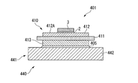
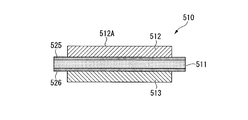
- FIG. 1 shows a power module substrate 10, a power module substrate 40 with a heat sink, and a power module 1 according to the first embodiment of the present invention.
- the power module 1 includes a power module substrate 10, a semiconductor element 3, and a heat sink 41.
- the power module substrate 10 is provided with a circuit layer 12.
- the semiconductor element 3 is bonded to the mounting surface 12 ⁇ / b> A of the circuit layer 12 via the solder layer 2.
- the solder layer 2 is made of, for example, Sn—Ag, Sn—In, or Sn—Ag—Cu solder (so-called lead-free solder).
- a Ni plating film (not shown) may be provided between the mounting surface 12 ⁇ / b> A of the circuit layer 12 and the solder layer 2.
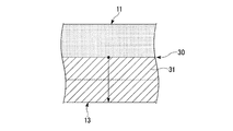
- the power module substrate 10 includes a ceramic substrate 11, a circuit layer 12, and a metal layer 13.
- the circuit layer 12 is formed on one surface (the upper surface in FIG. 1) of the ceramic substrate 11.
- the metal layer 13 is formed on the other surface (the lower surface in FIG. 1) of the ceramic substrate 11.
- the ceramic substrate 11 prevents electrical connection between the circuit layer 12 and the metal layer 13, and is made of highly insulating Al 2 O 3 (alumina). Further, the thickness of the ceramic substrate 11 is set within a range of 0.2 to 1.5 mm, and in this embodiment is set to 0.635 mm.
- the circuit layer 12 is formed by bonding a first copper plate 22 to one surface (upper surface in FIG. 6) of the ceramic substrate 11.
- the thickness of the circuit layer 12 is set in a range of 0.1 mm or more and 1.0 mm or less, and is set to 0.3 mm in the present embodiment.
- a circuit pattern is formed on the circuit layer 12, and one surface (the upper surface in FIG. 1) is a mounting surface 12A on which the semiconductor element 3 is mounted.
- the first copper plate 22 (circuit layer 12) is joined, at least one of an alkaline earth element, a transition metal element, and a rare earth element is added in a total of 1 molppm to 100 molppm, or boron is 100 molppm.
- the composition contains any one of 1000 molppm or less and the balance is copper and inevitable impurities, and more preferably at least one of at least one of an alkaline earth element, a transition metal element, and a rare earth element.
- the total content is 3 molppm or more and 50 molppm or less, or boron is contained in an amount of 300 molppm or more and 1000 molppm or less, and the oxygen content is 1 mass ppm or less.
- the first copper plate 22 (circuit layer 12) is made of Mg-Doped copper obtained by adding 15 molppm of Mg to oxygen-free copper (OFC) having a purity of 99.99 mass% or more.
- the metal layer 13 is formed by bonding an aluminum plate 23 to the other surface (the lower surface in FIG. 6) of the ceramic substrate 11.
- the aluminum plate 23 (metal layer 13) is a rolled plate of aluminum or aluminum alloy having a purity of 99% by mass or more and a proof stress of 30 N / mm 2 or less.
- the aluminum plate 23 (metal layer 13) is a rolled plate of aluminum (so-called 4N aluminum) having a purity of 99.99% by mass or more.
- any one of Si, Cu, Ag, Zn, Mg, Ge, Ca, Ga, Li or Two or more kinds of additive elements are in solid solution, and in this embodiment, Cu is in solution as the additive element.
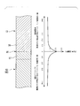
- a concentration gradient layer 31 is formed in which the concentration of the additive element (Cu concentration in the present embodiment) gradually decreases as the distance from the bonding interface 30 in the stacking direction is increased.
- the concentration of the additive element (Cu concentration in the present embodiment) on the bonding interface 30 side of the concentration gradient layer 31 (near the bonding interface 30 of the metal layer 13) is in the range of 0.01 mass% or more and 5 mass% or less. Is set to The concentration of the additive element in the vicinity of the bonding interface 30 of the metal layer 13 is an average value measured at 5 points from the bonding interface 30 by EPMA analysis (spot diameter of 30 ⁇ m). Further, the graph of FIG. 2B was obtained by performing line analysis in the stacking direction in the central portion of the metal layer 13 and using the concentration at the 50 ⁇ m position as a reference.
- the heat sink 41 cools the power module substrate 10 described above.
- the heat sink 41 in this embodiment includes a heat radiating plate 42 bonded to the other surface side of the metal layer 13 of the power module substrate 10.
- the heat radiating plate 42 is made of a metal material having a proof stress of 100 N / mm 2 or more and has a thickness of 2 mm or more.
- the heat radiating plate 42 is made of an A6063 alloy (aluminum alloy).
- the metal layer 13 and the heat sink 42 are made of Si, Cu, Ag, Zn, Mg, Ge, Ca, Ga, Li. Any one of these or two or more additional elements are in solid solution, and in this embodiment, Cu is dissolved as the additional element.
- concentration gradient layers 36 and 37 in which the concentration of the additive element (Cu concentration in this embodiment) gradually decreases as the distance from the bonding interface 35 in the stacking direction is formed.
- the concentration of the additive element (the Cu concentration in this embodiment) on the side of the bonding interface 35 of the concentration gradient layers 36 and 37 (near the bonding interface 35 of the metal layer 13 and the heat sink 42) is 0.01% by mass or more. It is set within the range of mass% or less.
- the concentration of the additive element in the vicinity of the bonding interface 35 between the metal layer 13 and the heat radiating plate 42 is an average value measured at 5 points from the bonding interface 35 by EPMA analysis (spot diameter 30 ⁇ m). Further, the graph of FIG. 3 was obtained by performing a line analysis in the stacking direction at the central portion of the metal layer 13 and the heat radiating plate 42 and using the concentration at the 50 ⁇ m position as a reference.
- the additive element concentration (Cu concentration) is set to be twice or more the additive element concentration (Cu concentration) in the metal layer 13.
- the thickness H of the high concentration element 32 is 4 nm or less.
- the bonding interface 30 to be observed here has a reference plane S at the center between the interface side end of the lattice image of the metal layer 13 and the end of the lattice image of the ceramic substrate 11. Further, the concentration (Cu concentration) of the additive element in the metal layer 13 is the concentration (Cu concentration) of the additive element in a portion of the metal layer 13 that is away from the bonding interface 30 by a certain distance (5 nm in this embodiment).
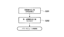
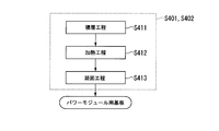
- the 1st copper plate 22 used as the circuit layer 12 and the ceramic substrate 11 are joined (circuit layer formation process S01). Since the ceramic substrate 11 is made of Al 2 O 3 , the liquid phase in the eutectic region of copper (Cu) and cuprous oxide (Cu 2 O) is used for the first copper plate 22 and the ceramic substrate 11. Bonding is performed by the DBC method (Direct Bonding Copper). Specifically, the first copper plate 22 and the ceramic substrate 11 are brought into contact with each other and heated at 1075 ° C. for 10 minutes in a nitrogen gas atmosphere to which a small amount of oxygen is added, whereby the first copper plate 22 and the ceramic substrate 11 are joined. Is done.
- DBC method Direct Bonding Copper
- first metal layer forming step S02 the aluminum plate 23 to be the metal layer 13 is joined to the other surface side of the ceramic substrate 11
- Heat sink joining step S03 the aluminum plate 23 and the heat radiating plate 42 of the heat sink 41 are joined.
- the first metal layer forming step S02 and the heat sink joining step S03 are performed simultaneously.
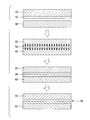
- the additive element (Cu) is fixed to one surface of the aluminum plate 23 by sputtering to form the first fixed layer 51, and the additive element (Cu) is fixed to the other surface of the aluminum plate 23 by sputtering to provide a second.
- the fixing layer 52 is formed (fixing layer forming step S11).
- the amount of additive element in the first fixed layer 51 and the second fixed layer 52 is in the range of 0.01 mg / cm 2 or more and 10 mg / cm 2 or less.
- Cu is used as the additive element.
- the amount of Cu in the first fixing layer 51 and the second fixing layer 52 is set to 0.08 mg / cm 2 or more and 2.7 mg / cm 2 or less.
- the aluminum plate 23 is laminated on the other surface side of the ceramic substrate 11. Furthermore, the heat radiating plate 42 is laminated on the other surface side of the aluminum plate 23 (lamination step S12). At this time, as shown in FIG. 6, the surface of the aluminum plate 23 on which the first fixing layer 51 is formed faces the ceramic substrate 11 and the surface of the aluminum plate 23 on which the second fixing layer 52 is formed. These are laminated so as to face the heat sink 42. That is, the first fixing layer 51 (additive element: Cu) is interposed between the aluminum plate 23 and the ceramic substrate 11, and the second fixing layer 52 (addition element: Cu) is interposed between the aluminum plate 23 and the heat dissipation plate 42. Is interposed.
- additive element: Cu additive element
- the first copper plate 22, the ceramic substrate 11, the aluminum plate 23, and the heat radiating plate 42 are charged in the stacking direction (pressure 1 to 35 kgf / cm 2 ) in a vacuum heating furnace and heated ( Heating step S13).
- the pressure in the vacuum heating furnace is set in the range of 10 ⁇ 3 to 10 ⁇ 6 Pa
- the heating temperature is set in the range of 550 ° C. to 650 ° C.
- a first molten metal region 55 is formed at the interface between the aluminum plate 23 and the ceramic substrate 11.
- the concentration of the additive element (Cu concentration) in the vicinity of the first fixed layer 51 of the aluminum plate 23 is diffused by diffusion of the additive element (Cu) of the first fixed layer 51 to the aluminum plate 23 side. Is formed by lowering the melting point.
- a second molten metal region 56 is formed at the interface between the aluminum plate 23 and the heat radiating plate 42.
- the second molten metal region 56 is formed in the vicinity of the second fixed layer 52 of the aluminum plate 23 and the heat sink 42 by diffusion of the additive element (Cu) of the second fixed layer 52 to the aluminum plate 23 side and the heat sink 42 side. This is formed by increasing the concentration of the additive element (Cu concentration) and lowering the melting point.
- the temperature is kept constant with the first molten metal region 55 and the second molten metal region 56 formed (molten metal solidification step S14).
- Cu in the first molten metal region 55 is further diffused toward the aluminum plate 23 side.
- the Cu concentration in the portion that was the first molten metal region 55 gradually decreases and the melting point increases, and solidification proceeds while the temperature is kept constant.
- the ceramic substrate 11 and the aluminum plate 23 are joined.
- Cu in the second molten metal region 56 further diffuses toward the aluminum plate 23 side and the heat sink 42 side, and the Cu concentration in the portion that was the second molten metal region 56 gradually decreases.
- the temperature rises solidification proceeds while the temperature is kept constant. Thereby, the aluminum plate 23 and the heat sink 42 are joined.
- the ceramic substrate 11 and the aluminum plate 23, and the aluminum plate 23 and the heat radiating plate 42 are joined by so-called Transient Liquid Phase Diffusing Bonding.
- the first copper plate 22, the ceramic substrate 11, the aluminum plate 23, and the heat sink 42 of the heat sink 41 are joined, and the power module substrate 10 and the power module substrate 40 with a heat sink according to the present embodiment. Is manufactured.
- the circuit layer 12 having the mounting surface 12A on which the semiconductor element 3 is mounted is configured by the first copper plate 22. Therefore, the heat generated from the semiconductor element 3 can be sufficiently expanded, and the dissipation of this heat can be promoted. As a result, electronic components such as the semiconductor element 3 having a high power density can be mounted, and the semiconductor package can be reduced in size and output.
- At least one of an alkaline earth element, a transition metal element, and a rare earth element is added in a total of 1 molppm to 100 molppm, or boron is 100 molppm.
- the composition contains any one of 1000 molppm or less and the balance is copper and inevitable impurities, and more preferably, at least one of alkaline earth elements, transition metal elements, and rare earth elements in total. 3 molppm or more and 50 molppm or less, or contains boron in an amount of 300 molppm or more and 1000 molppm or less.
- Mg- is obtained by adding 15 molppm of Mg to oxygen-free copper (OFC) having a purity of 99.99 mass% or more. Doped copper was used. Therefore, Mg reacts with S (sulfur) present in copper as one of the inevitable impurities to generate sulfide, and the influence of S can be suppressed. Thereby, the recrystallization temperature of the 1st copper plate 22 (circuit layer 12) becomes low, and work hardening is suppressed. Therefore, it is possible to suppress the occurrence of cracks in the ceramic substrate 11 during a cold cycle load. Further, the oxygen content of the first copper plate 22 (circuit layer 12) is 1 mass ppm or less. Therefore, it is suppressed that Mg reacts with oxygen and is consumed, and Mg and S can be reacted reliably.
- OFC oxygen-free copper
- the ceramic substrate 11 is made of Al 2 O 3 . Therefore, as described above, the first copper plate 22 and the ceramic substrate 11 are bonded by the DBC method (Direct Bonding Copper) using the liquid phase in the eutectic region of copper (Cu) and cuprous oxide (Cu 2 O). Can be joined. As a result, the bonding strength between the ceramic substrate 11 and the circuit layer 12 (first copper plate 22) can be secured, and the power module substrate 10 having excellent bonding reliability can be configured.
- DBC method Direct Bonding Copper
- the bonding interface 30 between the metal layer 13 and the ceramic substrate 11 and the bonding interface 35 between the metal layer 13 and the heat sink 42 of the heat sink 41 have Si, Cu, Ag, Zn, Mg, Ge, Ca, Ga. , Li are dissolved in one or more additional elements, and in this embodiment, Cu is dissolved as an additional element. Therefore, the joint interface 30 and 35 side portions of the metal layer 13 are solid solution strengthened, and breakage at the metal layer 13 portion can be prevented.
- the concentration of the additive element in the vicinity of the bonding interfaces 30 and 35 (Cu concentration in the present embodiment) is set within a range of 0.01% by mass to 5% by mass. Therefore, it is possible to prevent the strength in the vicinity of the bonding interfaces 30 and 35 of the metal layer 13 from becoming excessively high, and when the cooling cycle is applied to the power module substrate 10, thermal strain can be reduced by the metal layer 13. And the occurrence of cracks in the ceramic substrate 11 can be suppressed.
- the concentration of any one or more of additive elements of Si, Cu, Ag, Zn, Mg, Ge, Ca, Ga, Li is used.
- An additive element high concentration portion 32 is formed in which the Cu concentration in this embodiment is twice or more the concentration of the additive element in the metal layer 13. Therefore, it is possible to improve the bonding strength of the metal layer 13 by the additive element atoms (Cu atoms) existing in the vicinity of the interface.
- the heat sink 41 of the heat sink 41 is made of a metal material having a proof stress of 100 N / mm 2 or more and has a thickness of 2 mm or more.
- the heat sink 41 is made of an A6063 alloy (aluminum alloy). It is supposed to be. For this reason, rigidity is high and handling becomes easy.
- a metal layer 13 made of aluminum having a proof stress of 30 N / mm 2 or less (pure aluminum having a purity of 99.99% or more in this embodiment) is disposed between the heat sink 42 of the heat sink 41 and the ceramic substrate 11. Has been. Therefore, even if the heat dissipation plate 42 of the heat sink 41 has high rigidity, the thermal distortion caused by the difference in thermal expansion coefficient between the heat dissipation plate 42 of the heat sink 41 and the ceramic substrate 11 can be sufficiently relieved by the metal layer 13. Generation of cracks in the ceramic substrate 11 can be suppressed.
- the additive element (Cu) diffuses toward the aluminum plate 23 side and the heat radiating plate 42 side, so that the first joining interfaces 30 and 35 are formed.
- the molten metal region 55 and the second molten metal region 56 are formed, and the first molten metal region 55 and the second molten metal region 56 are joined by solidification, and are joined by so-called Transient Liquid Phase Bonding Bonding. Therefore, it is possible to manufacture the power module substrate 10 and the power module substrate 40 with a heat sink that can be firmly bonded under relatively low temperature conditions and have excellent bonding reliability.
- the amount of added elements in the first fixed layer 51 and the second fixed layer 52 formed on the bonding surface of the aluminum plate 23 is in the range of 0.01 mg / cm 2 to 10 mg / cm 2.
- Cu is used as an additive element, and the amount of Cu in the first fixed layer 51 and the second fixed layer 52 is set to 0.08 mg / cm 2 or more and 2.7 mg / cm 2 or less. Therefore, the 1st molten metal area
- the structure which performs 1st metal layer formation process S02 and heat sink joining process S03 simultaneously is set as the structure which performs 1st metal layer formation process S02 and heat sink joining process S03 simultaneously. Therefore, the joining process of both surfaces of the aluminum plate 23 can be performed once, and the manufacturing cost of the power module substrate 40 with a heat sink can be greatly reduced. Furthermore, unnecessary thermal load does not act on the ceramic substrate 11, and the occurrence of warpage or the like can be suppressed. Further, the first fixed layer 51 and the second fixed layer 52 are formed by fixing the additive element (Cu) to the bonding surface of the aluminum plate 23 by sputtering. Therefore, the additive element (Cu) can be reliably arranged on the bonding interfaces 30 and 35 of the aluminum plate 23.
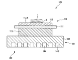
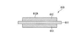
- a power module 101 shown in FIG. 9 includes a power module substrate 110, a semiconductor element 3, and a heat sink 141.
- a circuit layer 112 is disposed on the power module substrate 110.
- the semiconductor element 3 is bonded to the mounting surface 112 ⁇ / b> A of the circuit layer 112 via the solder layer 2.
- the power module substrate 110 includes a ceramic substrate 111, a circuit layer 112, and a metal layer 113.
- the circuit layer 112 is bonded to one surface (the upper surface in FIG. 9) of the ceramic substrate 111.
- the metal layer 113 is bonded to the other surface (the lower surface in FIG. 9) of the ceramic substrate 111.
- the ceramic substrate 111 is made of highly insulating AlN (aluminum nitride). Further, the thickness of the ceramic substrate 111 is set within a range of 0.2 to 1.5 mm, and in the present embodiment, is set to 0.635 mm.
- the circuit layer 112 is formed by bonding a first copper plate 122 to one surface of the ceramic substrate 111.
- the thickness of the circuit layer 112 is set within a range of 0.1 mm or more and 1.0 mm or less, and is set to 0.3 mm in the present embodiment.
- the first copper plate 122 (circuit layer 112) has the same configuration (composition) as the first copper plate 22 described in the first embodiment before being bonded.
- the first copper plate 122 (circuit layer 112) is Zr in which 10 mol ppm of Zr is added to oxygen-free copper (OFC) having a purity of 99.99% by mass or more instead of Mg described in the first embodiment. -Doped copper was used.
- the metal layer 113 is formed by bonding an aluminum plate 123 to the other surface of the ceramic substrate 111.
- This aluminum plate 123 (metal layer 113) is a rolled plate of aluminum or aluminum alloy having a purity of 99% by mass or more and a proof stress of 30 N / mm 2 or less.
- the aluminum plate 123 (metal layer 113) is a rolled plate of aluminum (so-called 4N aluminum) having a purity of 99.99% by mass or more.
- the heat sink 141 includes a top plate part 142 and a flow path 144.
- the top plate portion 142 is a portion of the top plate of the heat sink and is joined to the power module substrate 110.
- a cooling medium (for example, cooling water) flows through the flow path 144.
- the heat sink 141 (top plate portion 142) is preferably made of a material having good thermal conductivity, and it is necessary to ensure rigidity as a structural material. Therefore, in the present embodiment, the top plate portion 142 of the heat sink 141 is made of A6063 (aluminum alloy).
- one or more additive elements of Si, Cu, Ag, Zn, Mg, Ge, Ca, Ga, and Li are dissolved.
- Ag is dissolved as an additive element.
- a concentration gradient layer is formed in which the concentration of the additive element (Ag concentration in this embodiment) gradually decreases as the distance from the bonding interface in the stacking direction is increased.
- the concentration of the additive element (in the present embodiment, Ag concentration) on the bonding interface side (near the bonding interface of the metal layer 113) of this concentration gradient layer is set within a range of 0.01% by mass to 5% by mass. ing.
- the concentration of the additive element in the vicinity of the bonding interface of the metal layer 113 is an average value measured at 5 points from the bonding interface by EPMA analysis (spot diameter of 30 ⁇ m).
- any one of Si, Cu, Ag, Zn, Mg, Ge, Ca, Ga, and Li is provided on the metal layer 113 and the top plate portion 142.
- the seed or two or more additional elements are in solid solution, and in this embodiment, Ag is in solid solution as the additional element.
- a concentration gradient layer is formed in which the concentration of the additive element (Ag concentration in the present embodiment) gradually decreases as the distance from the bonding interface increases in the stacking direction.
- the concentration (additional Ag concentration in this embodiment) of the additive element on the bonding interface side (near the bonding interface between the metal layer 113 and the top plate 142) of the concentration gradient layer is 0.01 mass% or more and 5 mass% or less. It is set within the range.
- the concentration of the additive element in the vicinity of the bonding interface between the metal layer 113 and the top plate portion 142 is an average value measured at five points at a position of 50 ⁇ m from the bonding interface by EPMA analysis (spot diameter of 30 ⁇ m).
- the concentration (Ag concentration) of the additive element is set to be twice or more the concentration (Ag concentration) of the additive element in the metal layer 113.
- the thickness H of the high concentration portion of the additive element is 4 nm or less.
- the bonding interface to be observed here is based on the center between the interface side end of the lattice image of the metal layer 113 and the bonding interface side end of the lattice image of the ceramic substrate 111.
- the concentration (Ag concentration) of the additive element in the metal layer 113 is the concentration (Ag concentration) of the additive element in a portion of the metal layer 113 that is a fixed distance (5 nm in this embodiment) away from the bonding interface.
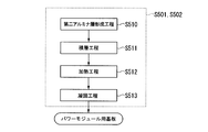
- an Al 2 O 3 layer 125 is formed on the surface of a ceramic substrate 111 made of AlN (first alumina layer forming step S100).
- the oxidation treatment of AlN was performed at 1200 ° C. or higher in an Ar—O 2 mixed gas atmosphere.
- the oxygen partial pressure P O2 and 10 kPa to prepare a water vapor partial pressure P H2 O to 0.05 kPa.
- a dense Al 2 O 3 layer 125 having excellent adhesion to AlN is formed.
- the thickness of the Al 2 O 3 layer 125 is 1 ⁇ m or more.
- the oxygen partial pressure was adjusted by mixing oxygen gas after deoxidizing high purity Ar gas. Moreover, after performing dehydration treatment by passing this atmospheric gas through a drying system filled with silica gel and diphosphorus pentoxide, the water vapor partial pressure was adjusted by passing water adjusted to a predetermined temperature.
- the 1st copper plate 122 used as the circuit layer 112 and the ceramic substrate 111 are joined (circuit layer formation process S101). Since the Al 2 O 3 layer 125 is formed on one surface of the ceramic substrate 111 made of AlN, the first copper plate 122 and the Al 2 O 3 layer 125 are made of copper (Cu) and cuprous oxide (Cu 2). Bonding is performed by a DBC method (Direct Bonding Copper) using a liquid phase in the eutectic region of O). Specifically, contacting the first copper plate 122 and the Al 2 O 3 layer 125, by heating 10 minutes at 1075 ° C. in a nitrogen gas atmosphere, and a first copper plate 122 and the Al 2 O 3 layer 125 Join.
- DBC method Direct Bonding Copper
- first metal layer forming step S102 the aluminum plate 123 to be the metal layer 113 is joined to the other surface side of the ceramic substrate 111 (first metal layer forming step S102), and the aluminum plate 123 and the heat sink 141 (top plate portion 142) are joined.
- Heat sink joining step S103 the first metal layer forming step S102 and the heat sink joining step S103 are performed simultaneously.
- the first fixed layer 151 is formed by fixing the additive element on one surface of the aluminum plate 123 by sputtering
- the second fixed layer 152 is formed by fixing the additive element on the other surface of the aluminum plate 123 by sputtering.
- the amount of additive element in the first fixed layer 151 and the second fixed layer 152 is in the range of 0.01 mg / cm 2 or more and 10 mg / cm 2 or less.
- Ag is used as the additive element.
- the Ag amount in the first fixing layer 151 and the second fixing layer 152 is set to 0.01 mg / cm 2 or more and 10 mg / cm 2 or less.
- an aluminum plate 123 is laminated on the other surface side of the ceramic substrate 111. Further, the top plate portion 142 is laminated on the other surface side of the aluminum plate 123 (lamination step S112). At this time, as shown in FIG. 12, the surface of the aluminum plate 123 on which the first fixing layer 151 is formed faces the ceramic substrate 111, and the surface of the aluminum plate 123 on which the second fixing layer 152 is formed. These are laminated so as to face the top plate part 142. That is, the first fixing layer 151 (additive element: Ag) is interposed between the aluminum plate 123 and the ceramic substrate 111, and the second fixing layer 152 (additive element: Ag) is interposed between the aluminum plate 123 and the top plate portion 142. ).
- the first fixing layer 151 additive element: Ag
- the second fixing layer 152 additive element: Ag
- the first copper plate 122, the ceramic substrate 111, the aluminum plate 123, and the top plate portion 142 are placed in a vacuum heating furnace while being pressurized in the stacking direction and heated (heating step S113).
- the pressure in the vacuum heating furnace is set in the range of 10 ⁇ 3 to 10 ⁇ 6 Pa, and the heating temperature is set in the range of 550 ° C. to 650 ° C.
- a first molten metal region is formed at the interface between the aluminum plate 123 and the ceramic substrate 111.
- the additive element concentration (Ag) in the vicinity of the first fixed layer 151 of the aluminum plate 123 is increased by the diffusion of the additive element (Ag) of the first fixed layer 151 toward the aluminum plate 123 side. It is formed by rising and lowering the melting point.
- a second molten metal region is formed at the interface between aluminum plate 123 and top plate portion 142.
- the additive element (Ag) of the second fixing layer 152 diffuses to the aluminum plate 123 side and the top plate portion 142 side, so that the second fixing layer 152 of the aluminum plate 123 and the top plate portion 142 is present. It is formed by increasing the concentration (Ag concentration) of the nearby additive element and lowering the melting point.
- the temperature is kept constant with the first molten metal region and the second molten metal region formed (molten metal solidification step S114).
- Ag in the first molten metal region is further diffused toward the aluminum plate 123 side.
- the Ag concentration in the portion that was the first molten metal region gradually decreases and the melting point increases, and solidification proceeds while the temperature is kept constant.
- the ceramic substrate 111 and the aluminum plate 123 are joined.
- Ag in the second molten metal region further diffuses toward the aluminum plate 123 side and the top plate portion 142 side, and the Ag concentration in the portion that was the second molten metal region gradually decreases and the melting point becomes lower.
- the temperature rises solidification proceeds while the temperature is kept constant. Thereby, the aluminum plate 123 and the top plate part 142 are joined.
- the ceramic substrate 111 and the aluminum plate 123, and the aluminum plate 123 and the top plate portion 142 are joined by so-called Transient Liquid Phase Diffusing Bonding. After solidification progresses in this way, cooling is performed to room temperature.
- the first copper plate 122, the ceramic substrate 111, the aluminum plate 123, and the heat sink 141 are joined, and the power module substrate 110 and the power module with the heat sink according to the present embodiment are used.
- a substrate 140 is manufactured.
- the circuit layer 112 is configured by the first copper plate 122. Therefore, heat from a heating element such as the semiconductor element 3 mounted on the mounting surface 112A of the circuit layer 112 can be efficiently promoted. Moreover, the circuit layer 112 is comprised with the 1st copper plate 122 containing 10 molppm of Zr. Therefore, Zr reacts with S (sulfur) present in copper as one of inevitable impurities to generate sulfides, and the influence of S can be suppressed. Thereby, the recrystallization temperature of the 1st copper plate 122 (circuit layer 112) becomes low, and work hardening is suppressed. Therefore, it is possible to suppress the occurrence of cracks in the ceramic substrate 111 during the cooling / heating cycle load.
- S sulfur
- an Al 2 O 3 layer 125 is formed on the surface of the ceramic substrate 111 made of AlN, and the first copper plate 122 and the ceramic substrate 111 are connected to each other by the DBC method using the Al 2 O 3 layer 125. Therefore, the first copper plate 122 and the ceramic substrate 111 can be firmly bonded. As described above, even if the ceramic substrate 111 is made of AlN, the first copper plate 122 can be bonded using the DBC method.
- the thickness of the Al 2 O 3 layer 125 to be formed is set to 1 ⁇ m or more. Therefore, the first copper plate 122 and the ceramic substrate 111 can be reliably bonded.
- the dense Al 2 O 3 layer 125 excellent in adhesion with AlN is formed by oxidizing AlN in a high oxygen partial pressure / low water vapor partial pressure atmosphere. Therefore, it is possible to prevent the occurrence of peeling between the ceramic substrate 111 made of AlN and the Al 2 O 3 layer 125.
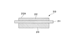
- a power module substrate 210 shown in FIG. 13 includes a ceramic substrate 211, a circuit layer 212, and a metal layer 213.
- the circuit layer 212 is formed on one surface (the upper surface in FIG. 13) of the ceramic substrate 211.
- the metal layer 213 is formed on the other surface (the lower surface in FIG. 13) of the ceramic substrate 211.
- the ceramic substrate 211 prevents electrical connection between the circuit layer 212 and the metal layer 213, and is made of highly insulating AlN. Further, the thickness of the ceramic substrate 211 is set within a range of 0.2 to 1.5 mm, and in the present embodiment, is set to 0.635 mm.
- the circuit layer 212 is formed by bonding a first copper plate 222 to one surface (upper surface in FIG. 15) of the ceramic substrate 211.
- the thickness of the circuit layer 212 is set within a range of 0.1 mm or more and 1.0 mm or less, and is set to 0.3 mm in the present embodiment.
- a circuit pattern is formed on the circuit layer 212, and one surface (the upper surface in FIG. 13) is a mounting surface 212A on which the semiconductor element 3 is mounted.
- the first copper plate 222 (circuit layer 212) is joined, at least one of an alkaline earth element, a transition metal element, and a rare earth element is added in a total of 1 molppm to 100 molppm, or boron is 100 molppm.
- the composition contains any one of 1000 molppm or less and the balance is copper and inevitable impurities, and more preferably, at least one of alkaline earth elements, transition metal elements, and rare earth elements in total. Either 3 mol ppm or more and 50 mol ppm or less or boron is contained in an amount of 300 mol ppm or more and 1000 mol ppm or less, and the oxygen content is 1 mass ppm or less.
- the first copper plate 222 (circuit layer 212) is made of La-doped copper in which 7 mol ppm of La is added to oxygen-free copper (OFC) having a purity of 99.99 mass% or more.
- the metal layer 213 is formed by bonding an aluminum plate 223 to the other surface (the lower surface in FIG. 15) of the ceramic substrate 211.
- the aluminum plate 223 (metal layer 213) is a rolled plate of aluminum or aluminum alloy having a purity of 99% by mass or more and a proof stress of 30 N / mm 2 or less.
- the aluminum plate 223 (metal layer 213) is a rolled plate of aluminum (so-called 4N aluminum) having a purity of 99.99% by mass or more.
- a method for manufacturing the power module substrate 210 having the above-described configuration will be described below.
- the 1st copper plate 222 used as the circuit layer 212 and the ceramic substrate 211 are joined (circuit layer formation process S201).
- the ceramic substrate 211 and the first copper plate 222 are joined by a so-called active metal method.
- a brazing material 225 made of Ag—Cu—Ti is disposed between a ceramic substrate 211 and a first copper plate 222, so that the ceramic substrate 211 and the first copper plate 222 are disposed. It is the method of joining.
- the brazing material 225 made of Ag-27.4 mass% Cu-2.0 mass% Ti is used, and the pressure is increased to 850 ° C. in a pressure of 10 ⁇ 3 Pa in the stacking direction.
- the ceramic substrate 211 and the first copper plate 222 are joined by heating for 10 minutes.
- the aluminum plate 223 to be the metal layer 213 is joined to the other surface side of the ceramic substrate 211 (first metal layer forming step S202).
- the ceramic substrate 211 and the aluminum plate 223 are bonded using an Al—Si brazing material.
- a brazing filler metal foil 226 of 15 to 30 ⁇ m (20 ⁇ m in this embodiment) is disposed between the ceramic substrate 211 and the aluminum plate 223 and pressed in the stacking direction.
- the aluminum plate 223 and the ceramic substrate 211 are joined by charging in a heating furnace in an N 2 gas atmosphere in the state and heating in a range of 550 ° C. to 650 ° C.
- the first copper plate 222, the ceramic substrate 211, and the aluminum plate 223 are joined together, and the power module substrate 210 according to this embodiment is manufactured.
- the circuit layer 212 is configured by the first copper plate 222. Therefore, heat from a heating element such as a semiconductor element mounted on the mounting surface 212A of the circuit layer 212 can be efficiently promoted.
- the circuit layer 212 is composed of a first copper plate 222 containing 7 mol ppm of La. Therefore, La reacts with S (sulfur) present in copper as one of inevitable impurities to generate a sulfide, and the influence of S can be suppressed. Thereby, the recrystallization temperature of the 1st copper plate 222 (circuit layer 212) becomes low, and work hardening is suppressed. Therefore, it is possible to suppress the occurrence of cracks in the ceramic substrate 211 when the thermal cycle is applied.
- the first copper plate 222 and the ceramic substrate 211 are joined by an active metal method using a brazing material 225 of Ag—Cu—Ti. Therefore, the power module substrate 210 can be configured without intervening oxygen at the interface between the first copper plate 222 and the ceramic substrate 211.
- the metal layer 313 may have a structure in which a plurality of aluminum plates 313A and 313B are stacked.
- stack may differ, and what was adjusted to the same magnitude
- the composition of these metal plates may be different.
- FIG. 17 shows a power module substrate 410, a power module substrate 440 with a heat sink, and a power module 401 according to the fifth embodiment of the present invention.
- the power module 401 includes a power module substrate 410, the semiconductor element 3, and a heat sink 441.
- the power module substrate 410 is provided with a circuit layer 412.
- the semiconductor element 3 is bonded to the mounting surface 412 ⁇ / b> A of the circuit layer 412 via the solder layer 2.
- the solder layer 2 is made of, for example, Sn—Ag, Sn—In, or Sn—Ag—Cu solder (so-called lead-free solder).
- a Ni plating film (not shown) may be provided between the mounting surface 412A of the circuit layer 412 and the solder layer 2.
- the power module substrate 410 includes a ceramic substrate 411, a circuit layer 412, and a metal layer 413, as shown in FIG.
- the circuit layer 412 is formed on one surface (the upper surface in FIG. 17) of the ceramic substrate 411.
- the metal layer 413 is formed on the other surface (the lower surface in FIG. 17) of the ceramic substrate 411.
- the ceramic substrate 411 prevents electrical connection between the circuit layer 412 and the metal layer 413, and is made of highly insulating Al 2 O 3 (alumina). Further, the thickness of the ceramic substrate 411 is set within a range of 0.2 to 1.5 mm, and in the present embodiment, is set to 0.635 mm.
- the circuit layer 412 is formed by bonding a first copper plate 422 to one surface (upper surface in FIG. 19) of the ceramic substrate 411.
- the thickness of the circuit layer 412 is set within a range of 0.1 mm or more and 1.0 mm or less, and is set to 0.3 mm in the present embodiment.
- a circuit pattern is formed on the circuit layer 412, and one surface (the upper surface in FIG. 17) is a mounting surface 412A on which the semiconductor element 3 is mounted.
- the metal layer 413 is formed by bonding a second copper plate 423 to the other surface (the lower surface in FIG. 19) of the ceramic substrate 411.
- the thickness of the metal layer 413 is set within a range of 0.1 mm or more and 1.0 mm or less, and is set to 0.3 mm in the present embodiment.
- Both the first copper plate 422 (circuit layer 412) and the second copper plate 423 (metal layer 413) have the same configuration (composition) as the first copper plate 22 described in the first embodiment before being joined.
- Mg-Doped copper obtained by adding 15 molppm of Mg to oxygen-free copper (OFC) having a purity of 99.99% by mass or more is used.
- the heat sink 441 cools the power module substrate 410 described above.
- the heat sink 441 in this embodiment includes a heat radiating plate 442 bonded to the other surface side of the metal layer 413 of the power module substrate 410.
- the heat sink 442 is made of an A6063 alloy (aluminum alloy).
- the metal layer 413 of the power module substrate 410 and the top plate portion of the heat sink 442 of the heat sink 441 are joined via a solder layer 405.
- the solder layer 405 is, for example, a Sn—Ag, Sn—In, or Sn—Ag—Cu based solder material (so-called lead-free solder material).
- the top plate portion of the heat dissipation plate 442 is joined to the other surface of the metal layer 413.
- the present invention is not particularly limited to this, and the other surface of the ceramic substrate 411 (the lower surface in FIG. 19)
- the heat sink 442 can also be brazed directly.
- circuit layer forming step S401 the first copper plate 422 to be the circuit layer 412 and the ceramic substrate 411 are joined (circuit layer forming step S401), and the second copper plate 423 to be the metal layer 413 and the ceramic substrate 411 Are joined (second metal layer forming step S402).
- circuit layer formation process S401 and 2nd metal layer formation process S402 are implemented simultaneously.
- the first copper plate 422 is laminated on one surface side of the ceramic substrate 411. Further, the second copper plate 423 is laminated on the other surface side of the ceramic substrate 411 (lamination step S411).
- the first copper plate 422, the ceramic substrate 411, and the second copper plate 423 are heated in an oxygen-containing atmosphere while being pressurized in the stacking direction (heating step S412).
- the heating temperature is set in the range of 1065 ° C. or more and 1083 ° C. or less.
- a first molten metal region 455 is formed at the interface between the first copper plate 422 and the ceramic substrate 411
- the second molten metal region is formed at the interface between the ceramic substrate 411 and the second copper plate 423.
- 456 is formed.
- the first molten metal region 455 and the second molten metal region 456 are formed by lowering the melting point due to a eutectic reaction between copper (Cu) and cuprous oxide (Cu 2 O).
- the first molten metal region 455 and the second molten metal region 456 are solidified by lowering the temperature (solidification step S413).
- the 1st copper plate 422, the ceramic substrate 411, and the 2nd copper plate 423 are joined, and the board
- the circuit layer 412 having the mounting surface 412A on which the semiconductor element 3 is mounted is configured by the first copper plate 422. Therefore, the heat generated from the semiconductor element 3 can be sufficiently expanded, and the dissipation of this heat can be promoted. As a result, electronic components such as the semiconductor element 3 having a high power density can be mounted, and the semiconductor package can be reduced in size and output.
- the same configuration (composition) as the first copper plate 22 described in the first embodiment. have.
- Mg-Doped copper obtained by adding 15 molppm of Mg to oxygen-free copper (OFC) having a purity of 99.99% by mass or more is used. Therefore, Mg reacts with S (sulfur) present in copper as one of the inevitable impurities to generate sulfide, and the influence of S can be suppressed. Thereby, the recrystallization temperature of the 1st copper plate 422 (circuit layer 412) and the 2nd copper plate 423 (metal layer 413) becomes low, and work hardening is suppressed.
- the oxygen content of the 1st copper plate 422 (circuit layer 412) and the 2nd copper plate 423 (metal layer 413) is 1 mass ppm or less. Therefore, it is suppressed that Mg reacts with oxygen and is consumed, and Mg and S can be reacted reliably.
- the ceramic substrate 411 is made of Al 2 O 3 . Therefore, as described above, the first and second copper plates 422 and 423 and the ceramic substrate 411 are combined using the DBC method using the liquid phase in the eutectic region of copper (Cu) and cuprous oxide (Cu 2 O) (The bonding can be performed by Direct Bonding Copper. Accordingly, the bonding strength between the ceramic substrate 411 and the circuit layer 412 (first copper plate 422) and between the ceramic substrate 411 and the metal layer 413 (second copper plate 423) can be ensured, and the power module excellent in bonding reliability can be obtained.
- the substrate 410 can be configured.
- the circuit layer forming step S401 and the second metal layer forming step S402 are simultaneously performed. Therefore, generation
- a power module substrate 510 shown in FIG. 20 includes a ceramic substrate 511, a circuit layer 512, and a metal layer 513.
- the circuit layer 512 is bonded to one surface (the upper surface in FIG. 20) of the ceramic substrate 511.
- the metal layer 513 is bonded to the other surface (the lower surface in FIG. 20) of the ceramic substrate 511.
- the ceramic substrate 511 is made of highly insulating AlN (aluminum nitride).
- the thickness of the ceramic substrate 511 is set within a range of 0.2 to 1.5 mm, and in this embodiment is set to 0.635 mm.
- Al 2 O 3 layers 525 and 526 are formed on one surface and the other surface of the ceramic substrate 511.
- the circuit layer 512 is formed by bonding a first copper plate 522 to one surface (upper surface in FIG. 22) of the ceramic substrate 511 as shown in FIG.
- the thickness of the circuit layer 512 is set within a range of 0.1 mm or more and 1.0 mm or less, and is set to 0.3 mm in the present embodiment.
- a circuit pattern is formed on the circuit layer 512, and one surface (the upper surface in FIG. 20) is a mounting surface 512A on which electronic components such as semiconductor elements are mounted.
- the metal layer 513 is formed by joining a second copper plate 523 to the other surface (the lower surface in FIG. 22) of the ceramic substrate 511.
- the thickness of the metal layer 513 is set within a range of 0.1 mm or more and 1.0 mm or less, and is set to 0.3 mm in the present embodiment.
- the first copper plate 522 (circuit layer 512) and the second copper plate 523 (metal layer 513) are made of oxygen-free copper (OFC) having a purity of 99.99% by mass or more as described in the first embodiment.
- OFC oxygen-free copper
- Zr-doped copper added with 10 mol ppm of Zr was used.
- the first copper plate 522 that becomes the circuit layer 512 and the ceramic substrate 511 are joined (circuit layer forming step S ⁇ b> 501), and the second copper plate 523 that becomes the metal layer 513. And the ceramic substrate 511 are joined (second metal layer forming step S502).
- the circuit layer forming step S501 and the second metal layer forming step S502 are performed simultaneously.
- Al 2 O 3 layers 525 and 526 are formed on one surface and the other surface of a ceramic substrate 511 made of AlN (second alumina layer forming step S510).
- AlN oxidation was performed at 1200 ° C. or higher in an Ar—O 2 mixed gas atmosphere.
- the oxygen partial pressure P O2 and 10 kPa to prepare a water vapor partial pressure P H2 O to 0.05 kPa.
- dense Al 2 O 3 layers 525 and 526 excellent in adhesion with AlN are formed.
- the thickness of the Al 2 O 3 layers 525 and 526 is 1 ⁇ m or more.
- the oxygen partial pressure was adjusted by mixing oxygen gas after deoxidizing high purity Ar gas. Moreover, after performing dehydration treatment by passing this atmospheric gas through a drying system filled with silica gel and diphosphorus pentoxide, the water vapor partial pressure was adjusted by passing water adjusted to a predetermined temperature.
- the first copper plate 522 is laminated on one surface side of the ceramic substrate 511. Further, the second copper plate 523 is laminated on the other surface side of the ceramic substrate 511 (lamination step S511). That is, the Al 2 O 3 layer 525 is interposed between the ceramic substrate 511 and the first copper plate 522, and the Al 2 O 3 layer 526 is interposed between the ceramic substrate 511 and the second copper plate 523.
- the first copper plate 522, the ceramic substrate 511, and the second copper plate 523 are heated in an oxygen-containing atmosphere in a state where they are pressurized in the stacking direction (heating step S512).
- the heating temperature is set in the range of 1065 ° C. or more and 1083 ° C. or less.
- a first molten metal region 555 is formed at the interface between the first copper plate 522 and the ceramic substrate 511
- the second molten metal region is formed at the interface between the ceramic substrate 511 and the second copper plate 523.
- 556 is formed.
- the first molten metal region 555 and the second molten metal region 556 are formed by lowering the melting point due to a eutectic reaction between copper (Cu) and cuprous oxide (Cu 2 O).
- the first molten metal region 555 and the second molten metal region 556 are solidified by lowering the temperature (solidification step S513).
- the 1st copper plate 522, the ceramic substrate 511, and the 2nd copper plate 523 are joined, and the board
- the circuit layer 512 is configured by the first copper plate 522. Therefore, heat from a heating element such as a semiconductor element mounted on the mounting surface 512A of the circuit layer 512 can be efficiently promoted.
- the circuit layer 512 and the metal layer 513 are composed of first and second copper plates 522 and 523 containing 10 mol ppm of Zr. Therefore, Zr reacts with S (sulfur) present in copper as one of inevitable impurities to generate sulfides, and the influence of S can be suppressed.
- the recrystallization temperature of the 1st copper plate 522 (circuit layer 512) and the 2nd copper plate 523 (metal layer 513) becomes low, and work hardening is suppressed. Therefore, it is possible to suppress the occurrence of cracks in the ceramic substrate 511 when the cooling / heating cycle is loaded.
- the Al 2 O 3 layer 525 is formed on one surface of the ceramic substrate 511 made of AlN, and the Al 2 O 3 layer 526 is formed on the other surface, and these Al 2 O 3 layers are formed. Since the first and second copper plates 522 and 523 and the ceramic substrate 511 are bonded by the DBC method using 525 and 526, the first and second copper plates 522 and 523 and the ceramic substrate 511 are firmly bonded. can do. As described above, even with the ceramic substrate 511 made of AlN, the first and second copper plates 522 and 523 can be bonded using the DBC method.
- the thickness of the Al 2 O 3 layers 525 and 526 to be formed is set to 1 ⁇ m or more. Therefore, the first and second copper plates 522 and 523 and the ceramic substrate 511 can be reliably bonded. Further, in the present embodiment, by performing oxidation treatment of AlN in a high oxygen partial pressure / low water vapor partial pressure atmosphere, dense Al 2 O 3 layers 525 and 526 having excellent adhesion with AlN are formed. Yes. Therefore, it is possible to prevent occurrence of peeling between the ceramic substrate 511 made of AlN and the Al 2 O 3 layers 525 and 526.
- a power module substrate 610 shown in FIG. 23 includes a ceramic substrate 611, a circuit layer 612, and a metal layer 613.
- the circuit layer 612 is formed on one surface (the upper surface in FIG. 23) of the ceramic substrate 611.
- the metal layer 613 is formed on the other surface (the lower surface in FIG. 23) of the ceramic substrate 611.
- the ceramic substrate 611 prevents electrical connection between the circuit layer 612 and the metal layer 613, and is made of highly insulating AlN. Further, the thickness of the ceramic substrate 611 is set within a range of 0.2 to 1.5 mm, and in the present embodiment, it is set to 0.635 mm.
- the circuit layer 612 is formed by bonding a first copper plate 622 to one surface of the ceramic substrate 611 (the upper surface in FIG. 25).
- the thickness of the circuit layer 612 is set within a range of 0.1 mm or more and 1.0 mm or less, and is set to 0.3 mm in the present embodiment.
- a circuit pattern is formed on the circuit layer 612, and one surface (the upper surface in FIG. 23) is a mounting surface 612A on which electronic components such as semiconductor elements are mounted.
- the metal layer 613 is formed by joining a second copper plate 623 to the other surface (the lower surface in FIG. 25) of the ceramic substrate 611.
- the thickness of the metal layer 613 is set within a range of 0.1 mm or more and 1.0 mm or less, and is set to 0.3 mm in the present embodiment.
- the first copper plate 622 (circuit layer 612) and the second copper plate 623 (metal layer 613) are made of oxygen-free copper (OFC) having a purity of 99.99% by mass or more as described in the first embodiment.
- OFC oxygen-free copper
- La-doped copper added with 7 mol ppm of La was used.
- the first copper plate 622 to be the circuit layer 612 and the ceramic substrate 611 are joined (circuit layer forming step S601), and the second copper plate 623 to be the metal layer 613. And the ceramic substrate 611 are bonded together (second metal layer forming step S602).
- the circuit layer forming step S601 and the second metal layer forming step S602 are performed simultaneously.
- the first and second copper plates 622 and 623 and the ceramic substrate 611 are joined by a so-called active metal method.
- the first copper plate 622 is laminated on one surface side of the ceramic substrate 611.
- the second copper plate 623 is laminated on the other surface side of the ceramic substrate 611 (lamination step S611).
- a brazing material 625 made of Ag—Cu—Ti is disposed between the first copper plate 622 and the ceramic substrate 611, and Ag is interposed between the ceramic substrate 611 and the second copper plate 623.
- a brazing material 626 made of -Cu-Ti is disposed.
- the brazing filler metals 625 and 626 are composed of Ag-27.4 mass% Cu-2.0 mass% Ti.
- the first copper plate 622, the ceramic substrate 611, and the second copper plate 623 are heated in a vacuum atmosphere while being pressurized in the stacking direction (heating step S612).
- heating was performed at 850 ° C. for 10 minutes in a vacuum atmosphere of 10 ⁇ 3 Pa.
- a first molten metal region 655 is formed at the interface between the first copper plate 622 and the ceramic substrate 611, and the second molten metal region is formed at the interface between the ceramic substrate 611 and the second copper plate 623. 656 is formed.
- the first molten metal region 655 and the second molten metal region 656 are solidified by lowering the temperature (solidification step S613).
- the 1st copper plate 622, the ceramic substrate 611, and the 2nd copper plate 623 are joined, and the board
- the circuit layer 612 is configured by the first copper plate 622. Therefore, heat from a heating element such as a semiconductor element mounted on the mounting surface 612A of the circuit layer 612 can be efficiently promoted.
- the circuit layer 612 and the metal layer 613 are comprised by the 1st and 2nd copper plates 622 and 623 containing 7 molppm La. Therefore, La reacts with S (sulfur) present in copper as one of inevitable impurities to generate a sulfide, and the influence of S can be suppressed.
- the recrystallization temperature of the 1st copper plate 622 (circuit layer 612) and the 2nd copper plate 623 (metal layer 613) becomes low, and work hardening is suppressed. As a result, it is possible to suppress the occurrence of cracks in the ceramic substrate 611 during a cooling / heating cycle load.
- the first and second copper plates 622 and 623 and the ceramic substrate 611 are joined by an active metal method using a brazing material 625 and 626 made of Ag—Cu—Ti. Therefore, the power module substrate 610 can be configured without interposing oxygen at the interface between the first and second copper plates 622 and 623 and the ceramic substrate 611.
- the ceramic substrate has been described as being composed of Al 2 O 3 and AlN
- the present invention is not limited to this and may be composed of Si 3 N 4 or the like.
- the aluminum plate constituting the metal layer has been described as a rolled plate of pure aluminum having a purity of 99.99% or more.
- the present invention is limited to this. There is no.
- the Al 2 O 3 layer is formed by oxidizing AlN.
- the present invention is not limited to this, and the surface of the ceramic substrate is not limited to this.
- an Al 2 O 3 layer may be formed.
- the additive element is fixed by sputtering, but the present invention is not limited to this, and it is added by vapor deposition, CVD, plating, or paste application. Elements may be fixed.
- the heat sink is described as being composed of an A6063 alloy, but the present invention is not limited to this, and the A1100 alloy, the A3003 alloy, the A5052 alloy, and the A7N01. It may be composed of another metal material such as an alloy.
- the structure of the heat sink is not limited to this embodiment, and a heat sink having another structure may be adopted.
- the configuration is described in which one power module substrate is bonded on the heat sink, but the present invention is not limited to this, and a plurality of power module substrates may be bonded on one heat sink. .
- the copper plate constituting the circuit layer and the copper plate constituting the metal layer have been described as having the same composition, but the present invention is not limited to this.
- the copper plate constituting the circuit layer and the copper plate constituting the metal layer may have different compositions.
- a 3 mm copper plate and a 1.6 mm thick aluminum plate made of 99.99% by mass aluminum (4NAl) were prepared. These ceramic substrate, copper plate, and aluminum plate were joined by the method described in the third embodiment.
- the pressure applied in the circuit layer forming step S201 was 0.5 gf / cm 2 and the heating temperature was 850 ° C.
- OFC oxygen-free copper
- A14 no crack was observed in the ceramic substrate when the cooling cycle was loaded 2000 times.
- ⁇ A13 no crack was observed in the ceramic substrate even when the cooling cycle was loaded 3000 times.
- the present invention example A5 and the present invention example A6 having different oxygen contents are compared, it is confirmed that the present invention example A5 having an oxygen content of 1 mass ppm or less has a higher cracking prevention effect on the ceramic substrate. It was done.
- a comparative experiment conducted to confirm the effectiveness of the present invention will be described.
- a ceramic substrate having a thickness of 0.635 mm made of Al 2 O 3 and a copper plate having a thickness of 0.3 mm made of copper or a copper alloy having the composition shown in Table 2 were prepared. These copper plate, ceramic substrate, and copper plate were joined by the method described in the seventh embodiment.
- the pressure applied in the circuit layer forming step S601 and the second metal layer forming step S602 was 0.5 kgf / cm 2 and the heating temperature was 850 ° C.
- OFC oxygen-free copper
- Invention Examples B1 to B1 containing at least one of alkaline earth elements, transition metal elements, and rare earth elements in a total of 1 mol ppm to 100 mol ppm, or boron from 100 mol ppm to 1000 mol ppm.
- B14 no crack was observed in the ceramic substrate when the cooling cycle was loaded 2000 times.
- B13 no cracks were observed in the ceramic substrate even when the cooling cycle was loaded 3000 times.
- the present invention example B5 and the present invention example B6 having different oxygen contents are compared, it is confirmed that the present invention example B5 having an oxygen content of 1 mass ppm or less has a higher cracking prevention effect on the ceramic substrate. It was done.
- Power module 3 Semiconductor element (electronic component) 10, 110, 210, 310, 410, 510, 610 Power module substrate 11, 111, 211, 311, 411, 511, 611 Ceramic substrate (insulating substrate) 12, 112, 212, 312, 412, 512, 612 Circuit layer 13, 113, 213, 313, 413, 513, 613 Metal layer 22, 122, 222, 422, 522, 622 First copper plate 423, 523, 623 First Copper plate 23, 123, 223 Aluminum plate 30 Bonding interface (ceramic substrate / metal layer) 32 High concentration part of additive element 35 Bonding interface (metal layer / heat sink) 40, 140, 340, 440 Power module substrate with heat sink 41, 141, 341, 441 Heat sink 125, 525, 526 Al 2 O 3 layers
Abstract
Description
本願は、2011年08月12日に日本に出願された特願2011-176712号及び特願2011-176881号に基づき優先権を主張し、その内容をここに援用する。
このようなパワーモジュール基板では、回路層の上に、はんだ材を介してパワー素子等の半導体素子が搭載される。
また、特許文献2、3には、第一の金属板(回路層)及び第二の金属板(金属層)を銅板とし、この銅板をDBC法によって絶縁基板に直接接合してなるパワーモジュール用基板が提案されている。また、特許文献2の第1図には、上述のパワーモジュール用基板に、有機系耐熱性接着剤用いてアルミニウム製のヒートシンクを接合したヒートシンク付パワーモジュール用基板が開示されている。
しかしながら、上述のパワーモジュール用基板においては、その使用環境において冷熱サイクルが負荷されるが、特許文献2,3に記載されているように回路層及び金属層を銅板で構成した場合には、上述の冷熱サイクルによって絶縁基板と銅板との熱膨張係数の差に起因するせん断応力が銅板に作用する。よって、銅板が加工硬化してしまい、絶縁基板に割れ等が発生するといった問題があった。
また、特許文献2に記載されたヒートシンク付パワーモジュール用基板においては、アルミニウム製のヒートシンクと絶縁基板との間に銅板が配設されている。このことから、ヒートシンクと絶縁基板との熱膨張係数の差に起因する熱歪みを、この銅板にて十分に緩和することができず、冷熱サイクル負荷時に絶縁基板に割れ等が生じやすいといった問題があった。
また、前記絶縁基板の他方の面に形成された金属層をさらに備えたパワーモジュール用基板であって、前記金属層は、前記絶縁基板の他方の面にアルミニウム板が接合されて構成されていてもよい。
このため、アルカリ土類元素、遷移金属元素、希土類元素又はボロンのうち少なくとも1種以上の元素が、不可避不純物のひとつとして銅中に存在するS(硫黄)と反応して硫化物を生成し、Sの影響を抑制することが可能となる。よって、冷熱サイクル時の特に高温域で、回路層において回復・再結晶化が進み、絶縁基板と回路層との熱膨張率の差に起因するせん断応力によって加工硬化された回路層の歪みが減少されることになり、冷熱サイクル時において絶縁基板に負荷される応力が低減される。これにより、冷熱サイクル負荷時における絶縁基板の割れの発生を抑制することが可能となる。
よって、アルカリ土類元素、遷移金属元素、希土類元素のうちの1種以上を合計で1molppm以上100molppm以下、又は、ボロンを100molppm以上1000molppm以下の範囲に設定している。
この場合、アルカリ土類元素、遷移金属元素、希土類元素の含有量の合計が3molppm以上、又は、ボロンの含有量が300molppm以上とされているので、銅中のSの影響を抑制することができ、再結晶温度が低くなり、加工硬化を確実に抑制することが可能となる。また、アルカリ土類元素、遷移金属元素、希土類元素の含有量の合計が50molppm以下、又は、ボロンの含有量が1000molppm以下とされているので、第一銅板の硬化や熱伝導度の低下を抑制することができる。
この場合、アルカリ土類元素、遷移金属元素、希土類元素又はボロンのうち少なくとも1種以上の元素が、酸素と反応して酸化物となることが抑制され、確実にSと反応し、硫化物を生成することができる。よって、アルカリ土類元素、遷移金属元素、希土類元素又はボロンのうち少なくとも1種以上の元素の含有量が少なくても、Sの影響を十分に抑制することが可能となる。
この場合、前記金属層に、Si,Cu,Ag,Zn,Mg,Ge,Ca,Ga及びLiのうちのいずれか1種又は2種以上の添加元素が固溶しているので、前記金属層の接合界面側部分が固溶強化される。これにより、金属層部分での破断を防止することができる。
この場合、金属層の接合界面に、前記添加元素の濃度が前記金属層中の前記添加元素の濃度の2倍以上とされた添加元素高濃度部が形成されているので、界面近傍に存在する前記添加元素原子により、金属層の接合強度の向上を図ることが可能となる。金属層中の前記添加元素の濃度とは、金属層のうち接合界面から一定距離(例えば、5nm以上)離れた部分における前記添加元素の濃度である。
このため、アルカリ土類元素、遷移金属元素、希土類元素又はボロンのうち少なくとも1種以上の元素が、不可避不純物のひとつとして銅中に存在するS(硫黄)と反応して硫化物を生成し、Sの影響を抑制することが可能となる。よって、冷熱サイクル時の特に高温域で、金属層において回復・再結晶化が進み、絶縁基板と回路層との熱膨張率の差に起因するせん断応力によって加工硬化された回路層の歪みが減少され、冷熱サイクル時において絶縁基板に負荷される応力が低減される。これにより、冷熱サイクル負荷時における絶縁基板の割れの発生を抑制することが可能となる。
この場合、アルカリ土類元素、遷移金属元素、希土類元素の含有量の合計が3molppm以上、又は、ボロンの含有量が300molppm以上とされているので、銅中のSの影響を抑制することができ、再結晶温度が低くなり、加工硬化を確実に抑制することが可能となる。また、アルカリ土類元素、遷移金属元素、希土類元素の含有量の合計が50molppm以下、又は、ボロンの含有量が1000molppm以下とされているので、前記第一銅板および/または前記第二銅板の硬化や熱伝導度の低下を抑制することができる。
この場合、アルカリ土類元素、遷移金属元素、希土類元素又はボロンのうち少なくとも1種以上の元素が、酸素と反応して酸化物となることが抑制され、確実にSと反応し、硫化物を生成することができる。よって、アルカリ土類元素、遷移金属元素、希土類元素又はボロンのうち少なくとも1種以上の元素の含有量が少なくても、Sの影響を十分に抑制することが可能となる。
この構成のパワーモジュール用基板によれば、アルミニウム板または第二銅板からなる金属層にヒートシンクが接合されている。よって、このヒートシンクによって、パワーモジュール用基板からの熱を効率良く放散することができる。また、冷熱サイクル負荷時の熱歪みを金属層の変形によって緩和することができ、絶縁基板の割れを抑制することができる。
また、本発明の他態様であるパワーモジュールは、前述のパワーモジュール用基板と、前記回路層上に搭載された電子部品と、を備えている。
これらの構成のパワーモジュールによれば、回路層上に搭載された電子部品からの熱を効率的に放散することができ、電子部品のパワー密度(発熱量)が向上した場合であっても、十分に対応することができる。
図1に本発明の第1の実施形態であるパワーモジュール用基板10、ヒートシンク付パワーモジュール用基板40及びパワーモジュール1を示す。
このパワーモジュール1は、パワーモジュール用基板10と、半導体素子3と、ヒートシンク41とを備えている。パワーモジュール用基板10は、回路層12が配設されている。半導体素子3は、回路層12の搭載面12Aにはんだ層2を介して接合されている。はんだ層2は、例えばSn-Ag系、Sn-In系、若しくはSn-Ag-Cu系のはんだ材(いわゆる無鉛はんだ材)とされている。本実施形態では、回路層12の搭載面12Aとはんだ層2との間に、Niめっき膜(図示なし)が設けられていてもよい。
本実施形態では、第一銅板22(回路層12)は、純度99.99質量%以上の無酸素銅(OFC)にMgを15molppm添加したMg-Doped銅を用いた。
このアルミニウム板23(金属層13)は、純度が99質量%以上で、耐力が30N/mm2以下のアルミニウム又はアルミニウム合金の圧延板とされている。
本実施形態においては、アルミニウム板23(金属層13)は、純度が99.99質量%以上のアルミニウム(いわゆる4Nアルミニウム)の圧延板とされている。
金属層13の接合界面30近傍には、接合界面30から積層方向に離間するにしたがい漸次添加元素の濃度(本実施形態ではCu濃度)が低下する濃度傾斜層31が形成されている。また、この濃度傾斜層31の接合界面30側(金属層13の接合界面30近傍)の添加元素の濃度(本実施形態ではCu濃度)が、0.01質量%以上5質量%以下の範囲内に設定されている。
金属層13の接合界面30近傍の添加元素の濃度は、EPMA分析(スポット径30μm)によって、接合界面30から50μmの位置で5点測定した平均値である。また、図2Bのグラフは、金属層13の中央部分において積層方向にライン分析を行い、前述の50μm位置での濃度を基準として求めた。
金属層13及び放熱板42の接合界面35近傍には、接合界面35から積層方向に離間するにしたがい漸次添加元素の濃度(本実施形態ではCu濃度)が低下する濃度傾斜層36、37が形成されている。また、この濃度傾斜層36、37の接合界面35側(金属層13及び放熱板42の接合界面35近傍)の添加元素の濃度(本実施形態ではCu濃度)が、0.01質量%以上5質量%以下の範囲内に設定されている。
この金属層13及び放熱板42の接合界面35近傍の添加元素の濃度は、EPMA分析(スポット径30μm)によって、接合界面35から50μmの位置で5点測定した平均値である。また、図3のグラフは、金属層13及び放熱板42の中央部分において積層方向にライン分析を行い、前述の50μm位置での濃度を基準として求めた。
このとき、図6に示すように、アルミニウム板23の第1固着層51が形成された面がセラミックス基板11を向くように、かつ、アルミニウム板23の第2固着層52が形成された面が放熱板42を向くようにして、これらを積層する。すなわち、アルミニウム板23とセラミックス基板11との間に第1固着層51(添加元素:Cu)を介在させ、アルミニウム板23と放熱板42との間に第2固着層52(添加元素:Cu)を介在させている。
また、図8に示すように、アルミニウム板23と放熱板42との界面に第2溶融金属領域56が形成される。この第2溶融金属領域56は、第2固着層52の添加元素(Cu)がアルミニウム板23側及び放熱板42側に拡散することによって、アルミニウム板23及び放熱板42の第2固着層52近傍の添加元素の濃度(Cu濃度)が上昇して融点が低くなることにより形成される。
この工程により、第1溶融金属領域55中のCuが、さらにアルミニウム板23側へと拡散していく。これにより、第1溶融金属領域55であった部分のCu濃度が徐々に低下していき融点が上昇することになり、温度を一定に保持した状態で凝固が進行していく。これにより、セラミックス基板11とアルミニウム板23とが接合される。
同様に、第2溶融金属領域56中のCuが、さらにアルミニウム板23側及び放熱板42側へと拡散し、第2溶融金属領域56であった部分のCu濃度が徐々に低下していき融点が上昇することになり、温度を一定に保持した状態で凝固が進行していく。これにより、アルミニウム板23と放熱板42とが接合される。
さらに、第一銅板22(回路層12)の酸素含有量が1質量ppm以下とされている。よって、Mgが酸素と反応して消費されることが抑制され、MgとSとを確実に反応させることができる。
また、スパッタリングにより、アルミニウム板23の接合面に添加元素(Cu)を固着させることで、第1固着層51及び第2固着層52を形成している。よって、アルミニウム板23の接合界面30、35に確実に添加元素(Cu)を配置することができる。
図9に示すパワーモジュール101は、パワーモジュール用基板110と、半導体素子3と、ヒートシンク141とを備えている。パワーモジュール用基板110は、回路層112が配設されている。半導体素子3は、回路層112の搭載面112Aにはんだ層2を介して接合されている。
この第一銅板122(回路層112)は、接合される前において、第1の実施形態に記載の第一銅板22と同様の構成(組成)を有している。本実施形態では、第一銅板122(回路層112)は、純度99.99質量%以上の無酸素銅(OFC)に、第1の実施形態に記載のMgの代わりにZrを10molppm添加したZr-Doped銅を用いた。
このアルミニウム板123(金属層113)は、純度が99質量%以上で、耐力が30N/mm2以下のアルミニウム又はアルミニウム合金の圧延板とされている。本実施形態においては、アルミニウム板123(金属層113)は、純度が99.99質量%以上のアルミニウム(いわゆる4Nアルミニウム)の圧延板とされている。
ヒートシンク141(天板部142)は、熱伝導性が良好な材質で構成されることが望ましく、かつ、構造材としての剛性を確保する必要がある。そこで、本実施形態においては、ヒートシンク141の天板部142は、A6063(アルミニウム合金)で構成されている。
金属層113の接合界面近傍には、接合界面から積層方向に離間するにしたがい漸次添加元素の濃度(本実施形態ではAg濃度)が低下する濃度傾斜層が形成されている。また、この濃度傾斜層の接合界面側(金属層113の接合界面近傍)の添加元素の濃度(本実施形態ではAg濃度)が、0.01質量%以上5質量%以下の範囲内に設定されている。
金属層113の接合界面近傍の添加元素の濃度は、EPMA分析(スポット径30μm)によって、接合界面から50μmの位置で5点測定した平均値である。
金属層113及び天板部142の接合界面近傍には、接合界面から積層方向に離間するにしたがい漸次添加元素の濃度(本実施形態ではAg濃度)が低下する濃度傾斜層が形成されている。また、この濃度傾斜層の接合界面側(金属層113及び天板部142の接合界面近傍)の添加元素の濃度(本実施形態ではAg濃度)が、0.01質量%以上5質量%以下の範囲内に設定されている。この金属層113及び天板部142の接合界面近傍の添加元素の濃度は、EPMA分析(スポット径30μm)によって、接合界面から50μmの位置で5点測定した平均値である。
ここで観察する接合界面は、金属層113の格子像の界面側端部とセラミックス基板111の格子像の接合界面側端部との間の中央を基準面とする。また、金属層113中の添加元素の濃度(Ag濃度)は、金属層113のうち接合界面から一定距離(本実施形態では5nm)離れた部分における添加元素の濃度(Ag濃度)である。
高純度のArガスを脱酸処理した後に酸素ガスを混合することによって酸素分圧を調整した。また、この雰囲気ガスをシリカゲルと五酸化二リンを充填した乾燥系に通すことで脱水処理を行った後に所定温度に調整された水中を通過させることによって水蒸気分圧を調整した。
このとき、図12に示すように、アルミニウム板123の第1固着層151が形成された面がセラミックス基板111を向くように、かつ、アルミニウム板123の第2固着層152が形成された面が天板部142を向くようにして、これらを積層する。すなわち、アルミニウム板123とセラミックス基板111との間に第1固着層151(添加元素:Ag)を介在させ、アルミニウム板123と天板部142との間に第2固着層152(添加元素:Ag)を介在させているのである。
また、アルミニウム板123と天板部142との界面に第2溶融金属領域が形成される。この第2溶融金属領域は、第2固着層152の添加元素(Ag)がアルミニウム板123側及び天板部142側に拡散することによって、アルミニウム板123及び天板部142の第2固着層152近傍の添加元素の濃度(Ag濃度)が上昇して融点が低くなることにより形成される。
この工程により、第1溶融金属領域中のAgが、さらにアルミニウム板123側へと拡散していく。これにより、第1溶融金属領域であった部分のAg濃度が徐々に低下していき融点が上昇することになり、温度を一定に保持した状態で凝固が進行していく。これにより、セラミックス基板111とアルミニウム板123とが接合される。
同様に、第2溶融金属領域中のAgが、さらにアルミニウム板123側及び天板部142側へと拡散し、第2溶融金属領域であった部分のAg濃度が徐々に低下していき融点が上昇することになり、温度を一定に保持した状態で凝固が進行していく。これにより、アルミニウム板123と天板部142とが接合される。
また、回路層112が、Zrを10molppm含有する第一銅板122で構成されている。よって、Zrが不可避不純物のひとつとして銅中に存在するS(硫黄)と反応して硫化物を生成し、Sの影響を抑制することが可能となる。これにより、第一銅板122(回路層112)の再結晶温度が低くなり、加工硬化が抑制される。よって、冷熱サイクル負荷時におけるセラミックス基板111の割れの発生を抑制することが可能となる。
また、本実施形態では、高酸素分圧/低水蒸気分圧雰囲気にてAlNの酸化処理を行うことにより、AlNとの密着性に優れた緻密なAl2O3層125を形成している。よって、AlNからなるセラミックス基板111とAl2O3層125との間での剥離の発生を防止することが可能となる。
図13に示すパワーモジュール用基板210は、セラミックス基板211と、回路層212と、金属層213と、を備えている。回路層212は、このセラミックス基板211の一方の面(図13において上面)に形成されている。金属層213は、セラミックス基板211の他方の面(図13において下面)に形成されている。
本実施形態では、第一銅板222(回路層212)は、純度99.99質量%以上の無酸素銅(OFC)にLaを7molppm添加したLa-Doped銅を用いた。
このアルミニウム板223(金属層213)は、純度が99質量%以上で、耐力が30N/mm2以下のアルミニウム又はアルミニウム合金の圧延板とされている。
本実施形態においては、アルミニウム板223(金属層213)は、純度が99.99質量%以上のアルミニウム(いわゆる4Nアルミニウム)の圧延板とされている。
まず、図14及び図15に示すように、回路層212となる第一銅板222とセラミックス基板211とを接合する(回路層形成工程S201)。セラミックス基板211と第一銅板222とは、いわゆる活性金属法によって接合されている。この活性金属法は、図15に示すように、セラミックス基板211と第一銅板222との間に、Ag-Cu-Tiからなるろう材225を配設して、セラミックス基板211と第一銅板222とを接合する方法である。
本実施形態では、Ag-27.4質量%Cu-2.0質量%Tiからなるろう材225を用いて、10-3Paの真空中にて、積層方向に加圧した状態で850℃にて10分加熱することによって、セラミックス基板211と第一銅板222とを接合している。
本実施形態では、図15に示すように、セラミックス基板211とアルミニウム板223との間に、15~30μm(本実施形態では20μm)のろう材箔226を配設し、積層方向に加圧した状態でN2ガス雰囲気の加熱炉内に装入して550℃以上650℃以下の範囲内に加熱することによって、アルミニウム板223とセラミックス基板211とを接合している。
また、回路層212が、Laを7molppm含有する第一銅板222で構成されている。よって、Laが不可避不純物のひとつとして銅中に存在するS(硫黄)と反応して硫化物を生成し、Sの影響を抑制することが可能となる。これにより、第一銅板222(回路層212)の再結晶温度が低くなり、加工硬化が抑制される。よって、冷熱サイクル負荷時におけるセラミックス基板211の割れの発生を抑制することが可能となる。
図16に示すように、金属層313を、複数のアルミニウム板313A、313Bを積層した構造としてもよい。図16では、2枚のアルミニウム板313A、313Bを積層させたものとしているが、積層する枚数に制限はない。また、図16に示すように、積層するアルミニウム板同士の大きさ、形状が異なっていても良いし、同じ大きさ、形状に調整されたものであってもよい。さらに、これらの金属板の組成が異なっていても良い。
このパワーモジュール401は、パワーモジュール用基板410と、半導体素子3と、ヒートシンク441とを備えている。パワーモジュール用基板410は、回路層412が配設されている。半導体素子3は、回路層412の搭載面412Aにはんだ層2を介して接合されている。はんだ層2は、例えばSn-Ag系、Sn-In系、若しくはSn-Ag-Cu系のはんだ材(いわゆる無鉛はんだ材)とされている。本実施形態では、回路層412の搭載面412Aとはんだ層2との間に、Niめっき膜(図示なし)が設けられていてもよい。
この工程により、図19に示すように、第一銅板422とセラミックス基板411との界面に第1溶融金属領域455が形成され、セラミックス基板411と第二銅板423との界面に第2溶融金属領域456が形成される。これら第1溶融金属領域455及び第2溶融金属領域456は、銅(Cu)と亜酸化銅(Cu2O)との共晶反応によって融点が降下することにより形成される。
このようして、第一銅板422、セラミックス基板411、第二銅板423が接合され、本実施形態であるパワーモジュール用基板410が製造される。
さらに、第一銅板422(回路層412)及び第二銅板423(金属層413)の酸素含有量が1質量ppm以下とされている。よって、Mgが酸素と反応して消費されることが抑制され、MgとSとを確実に反応させることができる。
図20に示すパワーモジュール基板510は、セラミックス基板511と、回路層512と、金属層513と、を備えている。回路層512は、このセラミックス基板511の一方の面(図20において上面)に接合されている。金属層513は、セラミックス基板511の他方の面(図20において下面)に接合されている。
また、このセラミックス基板511の一方の面及び他方の面には、Al2O3層525,526が形成されている。
高純度のArガスを脱酸処理した後に酸素ガスを混合することによって酸素分圧を調整した。また、この雰囲気ガスをシリカゲルと五酸化二リンを充填した乾燥系に通すことで脱水処理を行った後に所定温度に調整された水中を通過させることによって水蒸気分圧を調整した。
この工程により、図22に示すように、第一銅板522とセラミックス基板511との界面に第1溶融金属領域555が形成され、セラミックス基板511と第二銅板523との界面に第2溶融金属領域556が形成される。これら第1溶融金属領域555及び第2溶融金属領域556は、銅(Cu)と亜酸化銅(Cu2O)との共晶反応によって融点が降下することにより形成される。
このようして、第一銅板522、セラミックス基板511、第二銅板523が接合され、本実施形態であるパワーモジュール用基板510が製造される。
また、回路層512及び金属層513が、Zrを10molppm含有する第一および第二銅板522,523で構成されている。よって、Zrが不可避不純物のひとつとして銅中に存在するS(硫黄)と反応して硫化物を生成し、Sの影響を抑制することが可能となる。これにより、第一銅板522(回路層512)及び第二銅板523(金属層513)の再結晶温度が低くなり、加工硬化が抑制される。よって、冷熱サイクル負荷時におけるセラミックス基板511の割れの発生を抑制することが可能となる。
また、本実施形態では、高酸素分圧/低水蒸気分圧雰囲気にてAlNの酸化処理を行うことにより、AlNとの密着性に優れた緻密なAl2O3層525,526を形成している。よって、AlNからなるセラミックス基板511とAl2O3層525,526との間での剥離の発生を防止することが可能となる。
図23に示すパワーモジュール用基板610は、セラミックス基板611と、回路層612と、金属層613と、を備えている。回路層612は、このセラミックス基板611の一方の面(図23において上面)に形成されている。金属層613は、セラミックス基板611の他方の面(図23において下面)に形成されている。
まず、セラミックス基板611の一方の面側に第一銅板622を積層する。また、セラミックス基板611の他方の面側に第二銅板623を積層する(積層工程S611)。このとき、図25に示すように、第一銅板622とセラミックス基板611との間にAg-Cu-Tiからなるろう材625を配設し、セラミックス基板611と第二銅板623との間にAg-Cu-Tiからなるろう材626を配設する。
本実施形態では、ろう材625,626は、Ag-27.4質量%Cu-2.0質量%Tiの組成のものを用いた。
この工程により、図25に示すように、第一銅板622とセラミックス基板611との界面に第1溶融金属領域655が形成され、セラミックス基板611と第二銅板623との界面に第2溶融金属領域656が形成される。
このようして、第一銅板622、セラミックス基板611、第二銅板623が接合され、本実施形態であるパワーモジュール用基板610が製造される。
また、回路層612及び金属層613が、Laを7molppm含有する第一および第二銅板622,623で構成されている。よって、Laが不可避不純物のひとつとして銅中に存在するS(硫黄)と反応して硫化物を生成し、Sの影響を抑制することが可能となる。これにより、第一銅板622(回路層612)及び第二銅板623(金属層613)の再結晶温度が低くなり、加工硬化が抑制される。これによって、冷熱サイクル負荷時におけるセラミックス基板611の割れの発生を抑制することが可能となる。
例えば、セラミックス基板を、Al2O3、AlNで構成したもので説明したが、これに限定されることはなく、Si3N4等で構成されたものであってもよい。
また、第1、第2及び第3の実施形態では、金属層を構成するアルミニウム板を、純度99.99%以上の純アルミニウムの圧延板としたものとして説明したが、これに限定されることはない。
さらに、第1及び第2の実施形態における固着層形成工程において、スパッタによって添加元素を固着するものとして説明したが、これに限定されることはなく、蒸着、CVD、めっき又はペーストの塗布によって添加元素を固着させてもよい。
さらに、ヒートシンクの構造は、本実施形態に限定されることはなく、他の構造のヒートシンクを採用してもよい。
また、ヒートシンクの上に一つのパワーモジュール用基板が接合された構成として説明したが、これに限定されることはなく、一つのヒートシンクの上に複数のパワーモジュール用基板が接合されていてもよい。
AlNからなる厚さ0.635mmのセラミックス基板と、表1に示す組成の無酸素銅に任意の元素を添加したDoped銅、無酸素銅(OFC)、タプピッチ銅(TPC)からなる厚さ0.3mmの銅板と、純度99.99質量%のアルミニウム(4NAl)からなる厚さ1.6mmのアルミニウム板と、を準備した。
これらのセラミックス基板、銅板、アルミニウム板を、第3の実施形態に記載された方法により接合した。回路層形成工程S201における加圧圧力を0.5gf/cm2、加熱温度を850℃とした。また、第一金属層形成工程S202における加圧圧力を5kgf/cm2、加熱温度を640℃とした。
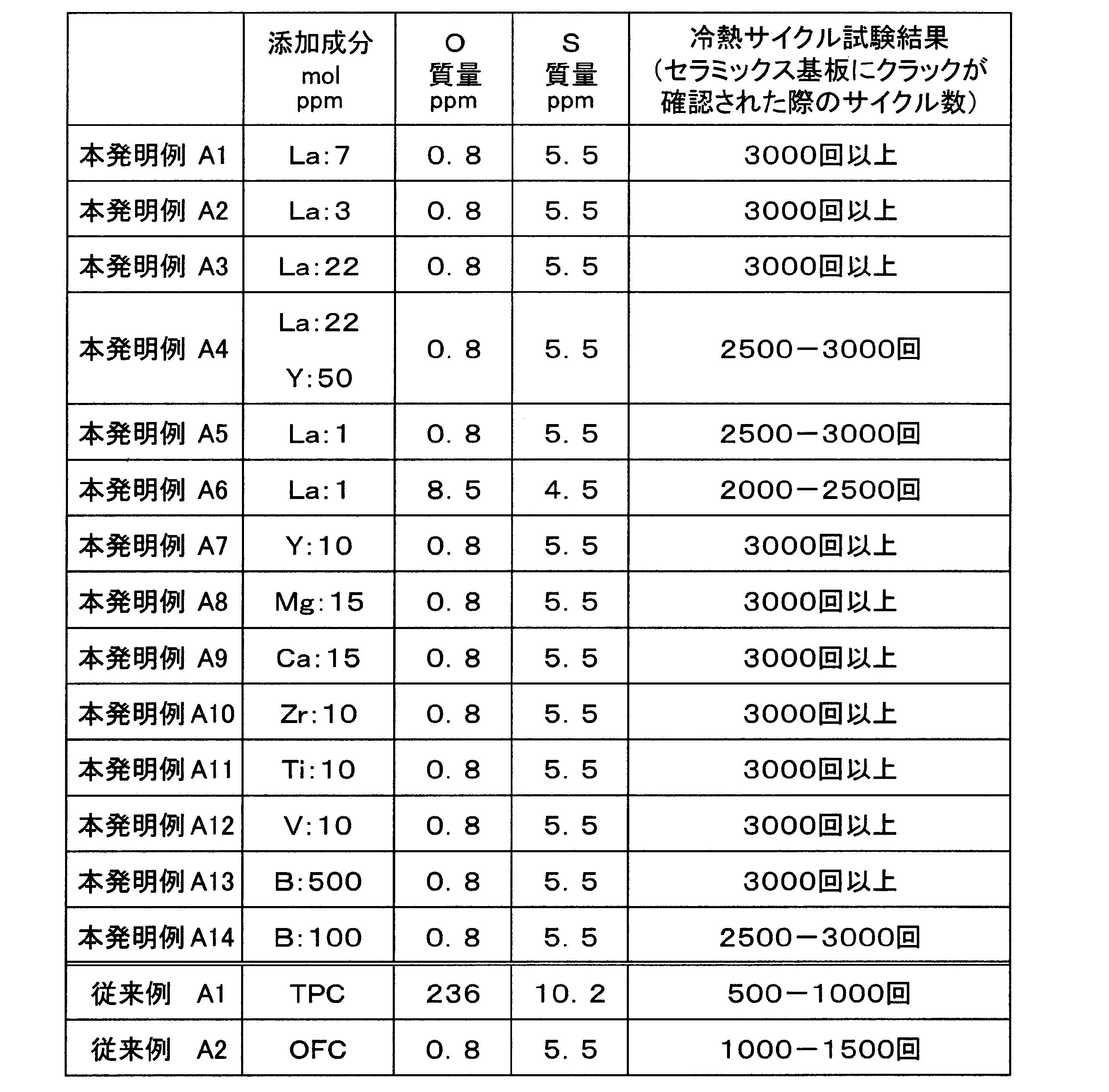
さらに、酸素含有量が異なる本発明例A5と本発明例A6とを比較すると、酸素含有量が1質量ppm以下とされた本発明例A5の方がセラミックス基板の割れ防止効果が高いことが確認された。
Al2O3からなる厚さ0.635mmのセラミックス基板と、表2に示す組成の銅又は銅合金からなる厚さ0.3mmの銅板と、を準備した。
これらの銅板、セラミックス基板、銅板を、第7の実施形態に記載された方法により接合した。回路層形成工程S601及び第二金属層形成工程S602における加圧圧力を0.5kgf/cm2、加熱温度を850℃とした。
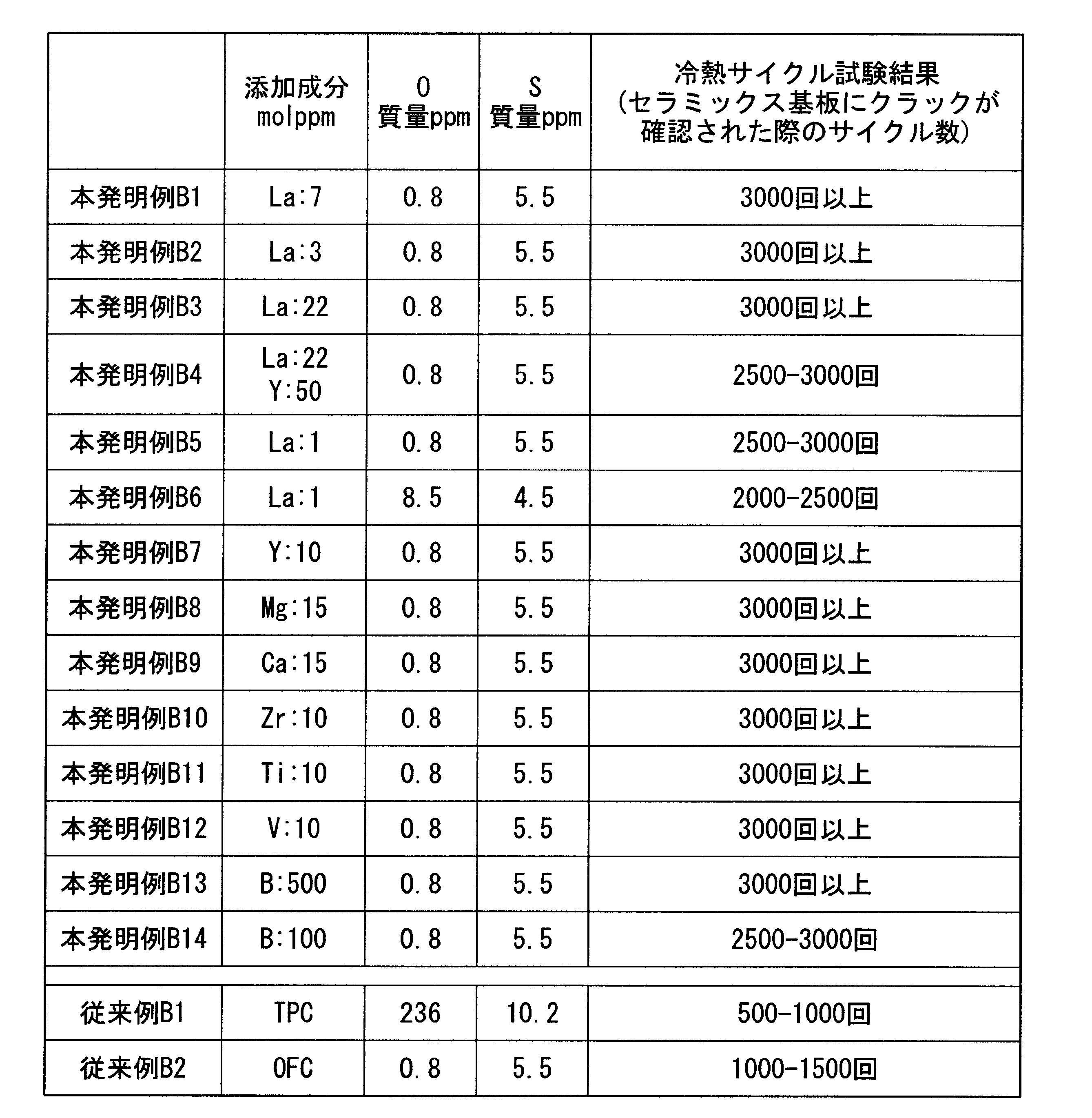
さらに、酸素含有量が異なる本発明例B5と本発明例B6とを比較すると、酸素含有量が1質量ppm以下とされた本発明例B5の方がセラミックス基板の割れ防止効果が高いことが確認された。
3 半導体素子(電子部品)
10、110、210、310、410、510、610 パワーモジュール用基板
11、111、211、311、411、511、611 セラミックス基板(絶縁基板)
12、112、212、312、412、512、612 回路層
13、113、213、313、413、513、613 金属層
22、122、222、422、522、622 第一銅板
423、523、623 第二銅板
23、123、223 アルミニウム板
30 接合界面(セラミックス基板/金属層)
32 添加元素高濃度部
35 接合界面(金属層/ヒートシンク)
40、140、340、440 ヒートシンク付パワーモジュール用基板
41、141、341、441 ヒートシンク
125、525,526 Al2O3層
Claims (13)
- 絶縁基板と、前記絶縁基板の一方の面に形成された回路層と、を備えたパワーモジュール用基板であって、
前記回路層は、前記絶縁基板の一方の面に第一銅板が接合されて構成されており、
前記第一銅板は、接合される前において、少なくとも、アルカリ土類元素、遷移金属元素、希土類元素のうちの1種以上を合計で1molppm以上100molppm以下、又は、ボロンを100molppm以上1000molppm以下のいずれか一方を含有し、残部が銅及び不可避不純物とされた組成とされていることを特徴とするパワーモジュール用基板。 - 前記絶縁基板の他方の面に形成された金属層をさらに備えたパワーモジュール用基板であって、前記金属層は、前記絶縁基板の他方の面にアルミニウム板が接合されて構成されている請求項1に記載のパワーモジュール用基板。
- 前記回路層を構成する第一銅板は、接合される前において、少なくとも、アルカリ土類元素、遷移金属元素、希土類元素のうちの1種以上を合計で3molppm以上50molppm以下、又は、ボロンを300molppm以上1000molppm以下のいずれか一方を含有し、残部が銅及び不可避不純物とされた組成とされている請求項1または2に記載のパワーモジュール用基板。
- 前記回路層を構成する第一銅板は、酸素含有量が1質量ppm以下とされている請求項1から3のいずれか一項に記載のパワーモジュール用基板。
- 前記金属層のうち前記絶縁基板との接合界面には、Si,Cu,Ag,Zn,Mg,Ge,Ca,Ga,Liのうちのいずれか1種又は2種以上の添加元素が固溶しており、前記金属層のうち接合界面近傍における前記添加元素の濃度の合計が0.01質量%以上5質量%以下の範囲内に設定されている請求項2から4のいずれか一項に記載のパワーモジュール用基板。
- 前記金属層のうち前記絶縁基板との接合界面には、Si,Cu,Ag,Zn,Mg,Ge,Ca,Ga,Liのうちのいずれか1種又は2種以上の添加元素の濃度が、前記金属層中の前記添加元素の濃度の2倍以上とされた添加元素高濃度部が形成されている請求項2から5のいずれか一項に記載のパワーモジュール用基板。
- 前記絶縁基板の他方の面に形成された金属層をさらに備えたパワーモジュール用基板であって、前記金属層は、前記絶縁基板の他方の面に第二銅板が接合されて構成されており、
前記第二銅板は、接合される前において、少なくとも、アルカリ土類元素、遷移金属元素、希土類元素のうちの1種以上を合計で1molppm以上100molppm以下、又は、ボロンを100molppm以上1000molppm以下のいずれか一方を含有し、残部が銅及び不可避不純物とされた組成とされている請求項1に記載のパワーモジュール用基板。 - 前記第一銅板および前記第二銅板の少なくとも一方は、接合される前において、少なくとも、アルカリ土類元素、遷移金属元素、希土類元素のうちの1種以上を合計で3molppm以上50molppm以下、又は、ボロンを300molppm以上1000molppm以下のいずれか一方を含有し、残部が銅及び不可避不純物とされた組成とされている請求項1または請求項7に記載のパワーモジュール用基板。
- 前記第一銅板および前記第二銅板の少なくとも一方は、酸素含有量が1質量ppm以下とされている請求項1、請求項7および8のいずれか一項に記載のパワーモジュール用基板。
- 請求項1から請求項9のいずれか一項に記載のパワーモジュール用基板と、前記絶縁基板の他方の面側に配設されたヒートシンクと、を備えたヒートシンク付パワーモジュール用基板。
- 請求項10に記載のヒートシンク付パワーモジュール用基板と、前記回路層上に搭載された電子部品と、を備えたヒートシンク付パワーモジュール。
- 請求項1から請求項9のいずれか一項に記載のパワーモジュール用基板と、前記回路層上に搭載された電子部品と、を備えたパワーモジュール。
- 絶縁基板と、この絶縁基板の一方の面に形成された回路層と、前記絶縁基板の他方の面に形成された金属層と、を備えたパワーモジュール用基板の製造方法であって、
前記回路層は、前記絶縁基板の一方の面に第一銅板が接合されて構成され、前記金属層は、前記絶縁基板の他方の面にアルミニウム板が接合されて構成され、前記第一銅板は、接合される前において、少なくとも、アルカリ土類元素、遷移金属元素、希土類元素のうちの1種以上を合計で1molppm以上100molppm以下、又は、ボロンを100molppm以上1000molppm以下のいずれか一方を含有し、残部が銅及び不可避不純物とされた組成とされており、
前記絶縁基板の一方の面に第一銅板を接合して前記回路層を形成する回路層形成工程と、
前記絶縁基板の他方の面にアルミニウム板を接合して前記金属層を形成する第一金属層形成工程と、を備え、
前記第一金属層形成工程においては、前記アルミニウム板の接合界面にSi,Cu,Ag,Zn,Mg,Ge,Ca,Ga,Liのうちのいずれか1種又は2種以上の添加元素を配置し、前記アルミニウム板を接合することを特徴とするパワーモジュール用基板の製造方法。
Priority Applications (4)
| Application Number | Priority Date | Filing Date | Title |
|---|---|---|---|
| US14/238,097 US9066433B2 (en) | 2011-08-12 | 2012-08-10 | Power module substrate, power module substrate with heat sink, power module, and method of manufacturing power module substrate |
| CN201280037162.1A CN103733329B (zh) | 2011-08-12 | 2012-08-10 | 功率模块用基板、自带散热器的功率模块用基板、功率模块以及功率模块用基板的制造方法 |
| EP12823914.2A EP2743978B1 (en) | 2011-08-12 | 2012-08-10 | Substrate for power module, substrate for power module with heat sink, power module, and method for manufacturing substrate for power module |
| KR1020147002677A KR101586157B1 (ko) | 2011-08-12 | 2012-08-10 | 파워 모듈용 기판, 히트 싱크가 형성된 파워 모듈용 기판, 파워 모듈 및 파워 모듈용 기판의 제조 방법 |
Applications Claiming Priority (4)
| Application Number | Priority Date | Filing Date | Title |
|---|---|---|---|
| JP2011-176881 | 2011-08-12 | ||
| JP2011176712A JP5765131B2 (ja) | 2011-08-12 | 2011-08-12 | パワーモジュール用基板、ヒートシンク付パワーモジュール用基板、パワーモジュール及びパワーモジュール用基板の製造方法 |
| JP2011176881A JP5699853B2 (ja) | 2011-08-12 | 2011-08-12 | パワーモジュール用基板、ヒートシンク付パワーモジュール用基板、パワーモジュール及びパワーモジュール用基板の製造方法 |
| JP2011-176712 | 2011-08-12 |
Publications (1)
| Publication Number | Publication Date |
|---|---|
| WO2013024813A1 true WO2013024813A1 (ja) | 2013-02-21 |
Family
ID=47715132
Family Applications (1)
| Application Number | Title | Priority Date | Filing Date |
|---|---|---|---|
| PCT/JP2012/070484 WO2013024813A1 (ja) | 2011-08-12 | 2012-08-10 | パワーモジュール用基板、ヒートシンク付パワーモジュール用基板、パワーモジュール及びパワーモジュール用基板の製造方法 |
Country Status (6)
| Country | Link |
|---|---|
| US (1) | US9066433B2 (ja) |
| EP (1) | EP2743978B1 (ja) |
| KR (1) | KR101586157B1 (ja) |
| CN (1) | CN103733329B (ja) |
| TW (1) | TWI575680B (ja) |
| WO (1) | WO2013024813A1 (ja) |
Cited By (7)
| Publication number | Priority date | Publication date | Assignee | Title |
|---|---|---|---|---|
| EP2838325A1 (en) * | 2013-08-16 | 2015-02-18 | NGK Insulators, Ltd. | Ceramic circuit board and electronic device |
| KR20160046808A (ko) * | 2013-08-26 | 2016-04-29 | 미쓰비시 마테리알 가부시키가이샤 | 접합체 및 파워 모듈용 기판 |
| EP3041042A1 (en) * | 2013-08-26 | 2016-07-06 | Mitsubishi Materials Corporation | Method for manufacturing assembly and method for manufacturing power-module substrate |
| CN106103386A (zh) * | 2014-04-25 | 2016-11-09 | 三菱综合材料株式会社 | 接合体的制造方法及功率模块用基板的制造方法 |
| US10173282B2 (en) | 2013-08-26 | 2019-01-08 | Mitsubishi Materials Corporation | Bonded body and power module substrate |
| WO2021187464A1 (ja) * | 2020-03-18 | 2021-09-23 | 三菱マテリアル株式会社 | 絶縁回路基板 |
| JP2021153180A (ja) * | 2020-03-18 | 2021-09-30 | 三菱マテリアル株式会社 | 絶縁回路基板 |
Families Citing this family (13)
| Publication number | Priority date | Publication date | Assignee | Title |
|---|---|---|---|---|
| US9414512B2 (en) * | 2009-10-22 | 2016-08-09 | Mitsubishi Materials Corporation | Substrate for power module, substrate with heat sink for power module, power module, method for producing substrate for power module, and method for producing substrate with heat sink for power module |
| JP6307832B2 (ja) * | 2013-01-22 | 2018-04-11 | 三菱マテリアル株式会社 | パワーモジュール用基板、ヒートシンク付パワーモジュール用基板、ヒートシンク付パワーモジュール |
| JP5720839B2 (ja) * | 2013-08-26 | 2015-05-20 | 三菱マテリアル株式会社 | 接合体及びパワーモジュール用基板 |
| JP5954371B2 (ja) * | 2014-08-05 | 2016-07-20 | 三菱マテリアル株式会社 | パワーモジュール用基板及びその製造方法 |
| DE102014220650A1 (de) * | 2014-10-13 | 2016-04-14 | Heraeus Deutschland GmbH & Co. KG | Optimiertes Leiterbahndesign von metallischen Materialien auf keramischen Substanzen |
| JP6729224B2 (ja) * | 2015-11-26 | 2020-07-22 | 三菱マテリアル株式会社 | セラミックス/アルミニウム接合体、絶縁回路基板、パワーモジュール、ledモジュール、熱電モジュール |
| WO2017115461A1 (en) * | 2015-12-28 | 2017-07-06 | Ngk Insulators, Ltd. | Bonded substrate and method for manufacturing bonded substrate |
| US10886251B2 (en) * | 2017-04-21 | 2021-01-05 | Toyota Motor Engineering & Manufacturing North America, Inc. | Multi-layered composite bonding materials and power electronics assemblies incorporating the same |
| CN113348046B (zh) | 2019-02-04 | 2022-10-04 | 三菱综合材料株式会社 | 铜-陶瓷接合体的制造方法、绝缘电路基板的制造方法、铜-陶瓷接合体及绝缘电路基板 |
| EP4071128B1 (en) * | 2019-12-02 | 2024-03-27 | Mitsubishi Materials Corporation | Copper/ceramic bonded body, insulating circuit board, method for producing copper/ceramic bonded body, and method for producing insulating circuit board |
| KR20210073296A (ko) | 2019-12-10 | 2021-06-18 | 삼성전자주식회사 | 공중부양 디스플레이 장치 |
| TWI759199B (zh) * | 2021-05-07 | 2022-03-21 | 艾姆勒車電股份有限公司 | 具有非矩形散熱層的散熱基材結構 |
| CN114918572B (zh) * | 2022-07-19 | 2022-11-04 | 北京理工大学 | 一种铝-铝的瞬态液相连接方法 |
Citations (11)
| Publication number | Priority date | Publication date | Assignee | Title |
|---|---|---|---|---|
| JPH0360184A (ja) * | 1989-07-28 | 1991-03-15 | Hitachi Cable Ltd | 銅配線セラミック基板の製造方法 |
| JPH0360185A (ja) * | 1989-07-28 | 1991-03-15 | Hitachi Cable Ltd | 銅配線セラミック基板の製造方法 |
| JPH03114289A (ja) * | 1989-09-28 | 1991-05-15 | Denki Kagaku Kogyo Kk | 銅回路を有する窒化アルミニウム基板の製造方法 |
| JPH0456754A (ja) * | 1990-06-22 | 1992-02-24 | Hitachi Cable Ltd | 耐屈曲用無酸素銅圧延箔と、これを用いたフレキシブルプリント基板及びtab用テープキャリア |
| JPH04162756A (ja) | 1990-10-26 | 1992-06-08 | Toshiba Corp | 半導体モジュール |
| JPH05170564A (ja) * | 1991-12-25 | 1993-07-09 | Kawasaki Steel Corp | 銅板接合AlN基板 |
| JP2000212660A (ja) * | 1999-01-18 | 2000-08-02 | Nippon Mining & Metals Co Ltd | フレキシブルプリント回路基板用圧延銅箔およびその製造方法 |
| JP3171234B2 (ja) | 1997-03-26 | 2001-05-28 | 三菱マテリアル株式会社 | ヒートシンク付セラミック回路基板 |
| JP3211856B2 (ja) | 1994-11-02 | 2001-09-25 | 電気化学工業株式会社 | 回路基板 |
| JP2011066405A (ja) * | 2009-08-19 | 2011-03-31 | Mitsubishi Materials Corp | パワーモジュール用基板の製造方法、パワーモジュール用基板、ヒートシンク付パワーモジュール用基板及びパワーモジュール |
| JP2011066385A (ja) * | 2009-03-31 | 2011-03-31 | Mitsubishi Materials Corp | パワーモジュール用基板、パワーモジュール及びパワーモジュール用基板の製造方法 |
Family Cites Families (8)
| Publication number | Priority date | Publication date | Assignee | Title |
|---|---|---|---|---|
| JPH03171234A (ja) | 1989-11-30 | 1991-07-24 | Seiko Epson Corp | クロック同期式記憶回路 |
| JPH03211856A (ja) | 1990-01-17 | 1991-09-17 | Fujitsu Ltd | 半導体装置製造データのシフト量の検査方法 |
| US6352743B1 (en) * | 1998-10-05 | 2002-03-05 | Kulicke & Soffa Investments, Inc. | Semiconductor copper band pad surface protection |
| US6566262B1 (en) * | 2001-11-01 | 2003-05-20 | Lsi Logic Corporation | Method for creating self-aligned alloy capping layers for copper interconnect structures |
| JP4254488B2 (ja) * | 2003-11-04 | 2009-04-15 | 日立電線株式会社 | 電子部品用銅箔及びその製造方法 |
| CN1603436A (zh) * | 2004-08-29 | 2005-04-06 | 陈行满 | 高强度无氧银铜合金材料的双层覆盖脱氧制造方法 |
| CN102047413B (zh) * | 2008-06-06 | 2015-04-15 | 三菱综合材料株式会社 | 功率模块用基板、功率模块以及功率模块用基板的制造方法 |
| JP2011094200A (ja) * | 2009-10-30 | 2011-05-12 | Jx Nippon Mining & Metals Corp | 銅又は銅合金箔、及びそれを用いた両面銅張積層板の製造方法 |
-
2012
- 2012-08-10 TW TW101128958A patent/TWI575680B/zh active
- 2012-08-10 WO PCT/JP2012/070484 patent/WO2013024813A1/ja active Application Filing
- 2012-08-10 US US14/238,097 patent/US9066433B2/en active Active
- 2012-08-10 EP EP12823914.2A patent/EP2743978B1/en active Active
- 2012-08-10 CN CN201280037162.1A patent/CN103733329B/zh active Active
- 2012-08-10 KR KR1020147002677A patent/KR101586157B1/ko active IP Right Grant
Patent Citations (11)
| Publication number | Priority date | Publication date | Assignee | Title |
|---|---|---|---|---|
| JPH0360184A (ja) * | 1989-07-28 | 1991-03-15 | Hitachi Cable Ltd | 銅配線セラミック基板の製造方法 |
| JPH0360185A (ja) * | 1989-07-28 | 1991-03-15 | Hitachi Cable Ltd | 銅配線セラミック基板の製造方法 |
| JPH03114289A (ja) * | 1989-09-28 | 1991-05-15 | Denki Kagaku Kogyo Kk | 銅回路を有する窒化アルミニウム基板の製造方法 |
| JPH0456754A (ja) * | 1990-06-22 | 1992-02-24 | Hitachi Cable Ltd | 耐屈曲用無酸素銅圧延箔と、これを用いたフレキシブルプリント基板及びtab用テープキャリア |
| JPH04162756A (ja) | 1990-10-26 | 1992-06-08 | Toshiba Corp | 半導体モジュール |
| JPH05170564A (ja) * | 1991-12-25 | 1993-07-09 | Kawasaki Steel Corp | 銅板接合AlN基板 |
| JP3211856B2 (ja) | 1994-11-02 | 2001-09-25 | 電気化学工業株式会社 | 回路基板 |
| JP3171234B2 (ja) | 1997-03-26 | 2001-05-28 | 三菱マテリアル株式会社 | ヒートシンク付セラミック回路基板 |
| JP2000212660A (ja) * | 1999-01-18 | 2000-08-02 | Nippon Mining & Metals Co Ltd | フレキシブルプリント回路基板用圧延銅箔およびその製造方法 |
| JP2011066385A (ja) * | 2009-03-31 | 2011-03-31 | Mitsubishi Materials Corp | パワーモジュール用基板、パワーモジュール及びパワーモジュール用基板の製造方法 |
| JP2011066405A (ja) * | 2009-08-19 | 2011-03-31 | Mitsubishi Materials Corp | パワーモジュール用基板の製造方法、パワーモジュール用基板、ヒートシンク付パワーモジュール用基板及びパワーモジュール |
Non-Patent Citations (1)
| Title |
|---|
| See also references of EP2743978A4 |
Cited By (16)
| Publication number | Priority date | Publication date | Assignee | Title |
|---|---|---|---|---|
| US10147663B2 (en) | 2013-08-16 | 2018-12-04 | Ngk Insulators, Ltd. | Ceramic circuit board and electronic device |
| EP2838325A1 (en) * | 2013-08-16 | 2015-02-18 | NGK Insulators, Ltd. | Ceramic circuit board and electronic device |
| KR102131484B1 (ko) | 2013-08-26 | 2020-07-07 | 미쓰비시 마테리알 가부시키가이샤 | 접합체 및 파워 모듈용 기판 |
| EP3041042A1 (en) * | 2013-08-26 | 2016-07-06 | Mitsubishi Materials Corporation | Method for manufacturing assembly and method for manufacturing power-module substrate |
| KR20160046808A (ko) * | 2013-08-26 | 2016-04-29 | 미쓰비시 마테리알 가부시키가이샤 | 접합체 및 파워 모듈용 기판 |
| EP3041045A4 (en) * | 2013-08-26 | 2017-03-29 | Mitsubishi Materials Corporation | Assembly and power-module substrate |
| EP3041042A4 (en) * | 2013-08-26 | 2017-03-29 | Mitsubishi Materials Corporation | Method for manufacturing assembly and method for manufacturing power-module substrate |
| US9648737B2 (en) | 2013-08-26 | 2017-05-09 | Mitsubishi Materials Corporation | Bonded body and power module substrate |
| US9905437B2 (en) | 2013-08-26 | 2018-02-27 | Mitsubishi Materials Corporation | Method of producing bonded body and method of producing power module substrate |
| EP3041045A1 (en) * | 2013-08-26 | 2016-07-06 | Mitsubishi Materials Corporation | Assembly and power-module substrate |
| US10173282B2 (en) | 2013-08-26 | 2019-01-08 | Mitsubishi Materials Corporation | Bonded body and power module substrate |
| US10370303B2 (en) | 2014-04-25 | 2019-08-06 | Mitsubishi Materials Corporation | Process for producing bonded body and process for producing power module substrate |
| CN106103386A (zh) * | 2014-04-25 | 2016-11-09 | 三菱综合材料株式会社 | 接合体的制造方法及功率模块用基板的制造方法 |
| WO2021187464A1 (ja) * | 2020-03-18 | 2021-09-23 | 三菱マテリアル株式会社 | 絶縁回路基板 |
| JP2021153180A (ja) * | 2020-03-18 | 2021-09-30 | 三菱マテリアル株式会社 | 絶縁回路基板 |
| EP4123697A4 (en) * | 2020-03-18 | 2024-04-24 | Mitsubishi Materials Corp | INSULATED CIRCUIT BOARD |
Also Published As
| Publication number | Publication date |
|---|---|
| TWI575680B (zh) | 2017-03-21 |
| US20140192486A1 (en) | 2014-07-10 |
| US9066433B2 (en) | 2015-06-23 |
| KR20140041817A (ko) | 2014-04-04 |
| EP2743978A4 (en) | 2015-07-29 |
| TW201322385A (zh) | 2013-06-01 |
| EP2743978A1 (en) | 2014-06-18 |
| CN103733329A (zh) | 2014-04-16 |
| EP2743978B1 (en) | 2018-05-02 |
| KR101586157B1 (ko) | 2016-01-15 |
| CN103733329B (zh) | 2016-10-26 |
Similar Documents
| Publication | Publication Date | Title |
|---|---|---|
| WO2013024813A1 (ja) | パワーモジュール用基板、ヒートシンク付パワーモジュール用基板、パワーモジュール及びパワーモジュール用基板の製造方法 | |
| WO2013147142A1 (ja) | パワーモジュール用基板、ヒートシンク付パワーモジュール用基板及びパワーモジュール | |
| JP5577980B2 (ja) | ヒートシンク付パワーモジュール用基板、パワーモジュール及びヒートシンク付パワーモジュール用基板の製造方法 | |
| WO2011030754A1 (ja) | ヒートシンク付パワーモジュール用基板の製造方法、ヒートシンク付パワーモジュール用基板及びパワーモジュール | |
| WO2014157112A1 (ja) | パワーモジュール用基板、ヒートシンク付パワーモジュール用基板及びパワーモジュール | |
| WO2011049067A1 (ja) | パワーモジュール用基板、ヒートシンク付パワーモジュール用基板、パワーモジュール、パワーモジュール用基板の製造方法及びヒートシンク付パワーモジュール用基板の製造方法 | |
| JP5935292B2 (ja) | パワーモジュール用基板の製造方法、ヒートシンク付パワーモジュール用基板の製造方法 | |
| JP5504842B2 (ja) | パワーモジュール用基板、ヒートシンク付パワーモジュール用基板、パワーモジュール及びパワーモジュール用基板の製造方法 | |
| JP2014222788A (ja) | パワーモジュール用基板の製造方法、ヒートシンク付パワーモジュール用基板の製造方法及びパワーモジュールの製造方法 | |
| JP5278354B2 (ja) | パワーモジュール用基板、パワーモジュール用基板の製造方法、ヒートシンク付パワーモジュール用基板及びパワーモジュール | |
| JP5699853B2 (ja) | パワーモジュール用基板、ヒートシンク付パワーモジュール用基板、パワーモジュール及びパワーモジュール用基板の製造方法 | |
| JP2011119652A (ja) | ヒートシンク付パワーモジュール用基板の製造方法、ヒートシンク付パワーモジュール用基板及びパワーモジュール | |
| JP5910166B2 (ja) | パワーモジュール用基板の製造方法 | |
| JP5765131B2 (ja) | パワーモジュール用基板、ヒートシンク付パワーモジュール用基板、パワーモジュール及びパワーモジュール用基板の製造方法 | |
| JP6819299B2 (ja) | 接合体、パワーモジュール用基板、接合体の製造方法及びパワーモジュール用基板の製造方法 | |
| JP5640569B2 (ja) | パワーモジュール用基板の製造方法 | |
| JP6432373B2 (ja) | ヒートシンク付パワーモジュール用基板、パワーモジュール、及び、ヒートシンク付パワーモジュール用基板の製造方法 | |
| CN108701659B (zh) | 接合体、功率模块用基板、功率模块、接合体的制造方法及功率模块用基板的制造方法 | |
| JP5724273B2 (ja) | パワーモジュール用基板、ヒートシンク付パワーモジュール用基板、パワーモジュール、パワーモジュール用基板の製造方法及びヒートシンク付パワーモジュール用基板の製造方法 | |
| JP2017135374A (ja) | 接合体、パワーモジュール用基板、パワーモジュール、接合体の製造方法及びパワーモジュール用基板の製造方法 | |
| JP2011119653A (ja) | ヒートシンク付パワーモジュール用基板の製造方法、ヒートシンク付パワーモジュール用基板及びパワーモジュール | |
| WO2017126641A1 (ja) | 接合体、パワーモジュール用基板、接合体の製造方法及びパワーモジュール用基板の製造方法 | |
| JP2015070098A (ja) | 銅板付きパワーモジュール用基板、及び銅板付きパワーモジュール用基板の製造方法 | |
| JP5359942B2 (ja) | パワーモジュール用基板、パワーモジュール及びパワーモジュール用基板の製造方法 | |
| JP5640571B2 (ja) | パワーモジュール用基板の製造方法 |
Legal Events
| Date | Code | Title | Description |
|---|---|---|---|
| 121 | Ep: the epo has been informed by wipo that ep was designated in this application |
Ref document number: 12823914 Country of ref document: EP Kind code of ref document: A1 |
|
| ENP | Entry into the national phase |
Ref document number: 20147002677 Country of ref document: KR Kind code of ref document: A |
|
| WWE | Wipo information: entry into national phase |
Ref document number: 2012823914 Country of ref document: EP |
|
| WWE | Wipo information: entry into national phase |
Ref document number: 14238097 Country of ref document: US |
|
| NENP | Non-entry into the national phase |
Ref country code: DE |